

Ultra low drop BICMOS voltage regulator
Feature summary
■ 0.8A Guaranteed output current
■ Ultra low dropout voltage (150mV typ. @ 0.8A
load, 20mV typ. @150mA load)
■ Very low quiescent current (1mA typ. @ 0.8A
load, 1µA max @ 25°C in off mode)
■ Logic-controlled electronic shutdown
■ Current and thermal internal limit
■ ±1.5% Output voltage tolerance @ 25°C
■ Fixed and ADJ output voltages: 1.22V, 1.8V,
2.5V, 3.3V, ADJ. (*see order code)
■ Temperature range: -40 to 125°C
■ Fast dynamic response to line and load
changes
■ Stable with ceramic capacitor (see paragraph
7.1, 7.2, 7.3)
■ Available in PPAK, DPAK and DFN8 (4x4mm)
Typical application
■ Microprocessor power supply
■ DSPs power supply
■ Post regulators for switching suppliers
■ High efficiency linear regulator
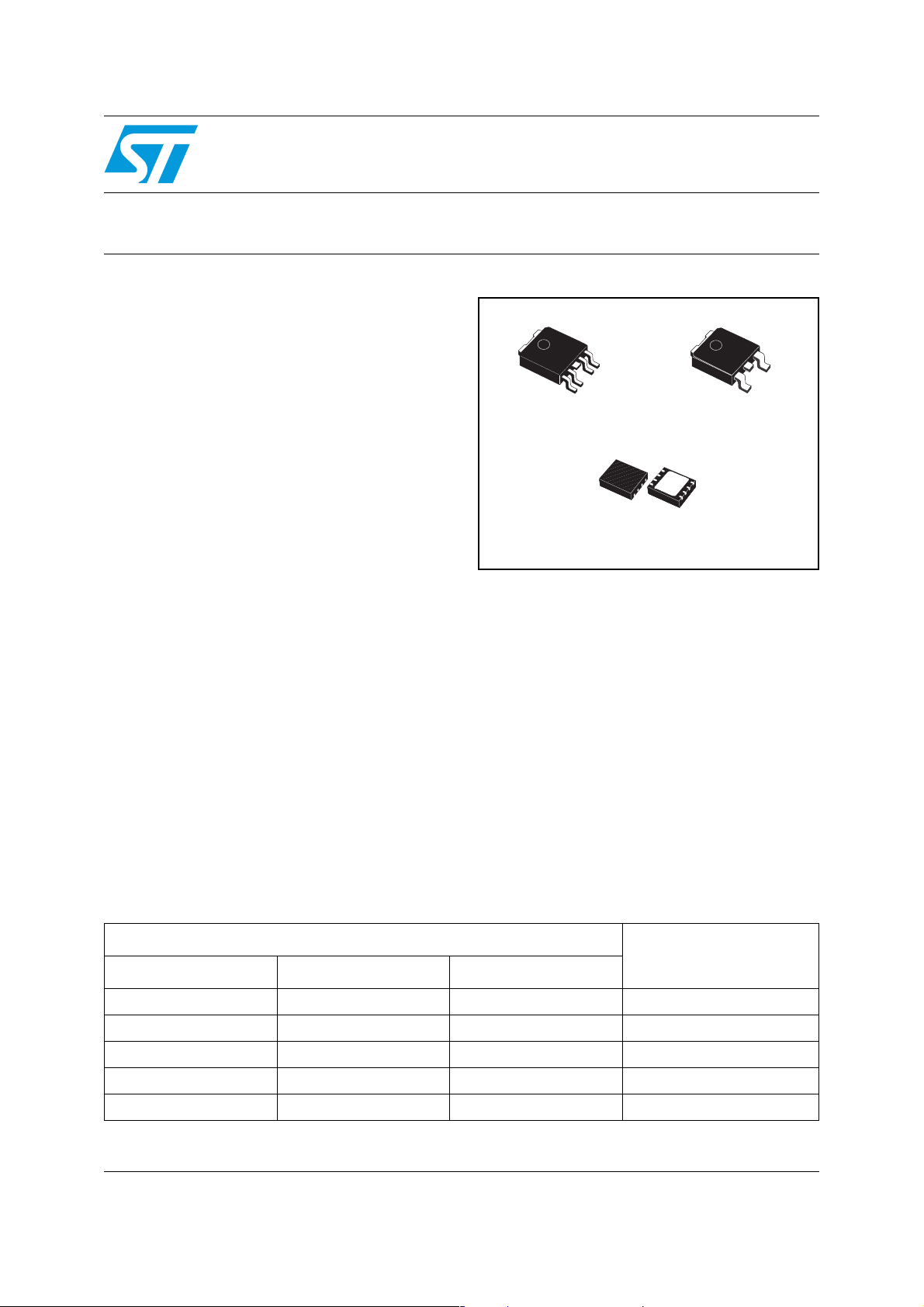
LD39080
PPAK
DFN8 (4x4 mm)
Description
The LD39080 is a fast ultra low drop linear
regulator which operates from 2.5V to 6V input
supply.
A wide range of output options are available. The
low drop voltage, low noise, and ultra low
quiescent current make it suitable for low voltage
microprocessor and memory applications. The
device is developed on a BiCMOS process which
allows low quiescent current operation
independently of output load current.
DPAK
Order codes
Part numbers
DPAK (T&R) PPAK (T&R) DFN
LD39080DT12-R LD39080PU12R 1.22V
LD39080DT18-R LD39080PT18-R LD39080PU18R 1.8V
LD39080DT25-R LD39080PT25-R LD39080PU25R 2.5V
LD39080DT33-R LD39080PT33-R LD39080PU33R 3.3V
LD39080PT-R LD39080PU-R ADJ From 1.22 to 5.0V
1. Available on request
January 2007 Rev. 1 1/20
(1)
Output voltage
www.st.com
20

LD39080
Contents
1 Diagram . . . . . . . . . . . . . . . . . . . . . . . . . . . . . . . . . . . . . . . . . . . . . . . . . . . 3
2 Pin configuration . . . . . . . . . . . . . . . . . . . . . . . . . . . . . . . . . . . . . . . . . . . 4
3 Typical application circuits . . . . . . . . . . . . . . . . . . . . . . . . . . . . . . . . . . . 5
4 Maximum ratings . . . . . . . . . . . . . . . . . . . . . . . . . . . . . . . . . . . . . . . . . . . . 7
5 Electrical characteristics . . . . . . . . . . . . . . . . . . . . . . . . . . . . . . . . . . . . . 8
6 Typical performance characteristics . . . . . . . . . . . . . . . . . . . . . . . . . . . . 9
7 Application notes . . . . . . . . . . . . . . . . . . . . . . . . . . . . . . . . . . . . . . . . . . 12
7.1 External capacitors . . . . . . . . . . . . . . . . . . . . . . . . . . . . . . . . . . . . . . . . . . 12
7.2 Input capacitor . . . . . . . . . . . . . . . . . . . . . . . . . . . . . . . . . . . . . . . . . . . . . 12
7.3 Output capacitor . . . . . . . . . . . . . . . . . . . . . . . . . . . . . . . . . . . . . . . . . . . . 12
7.4 Thermal note . . . . . . . . . . . . . . . . . . . . . . . . . . . . . . . . . . . . . . . . . . . . . . 12
7.5 Inhibit input operation . . . . . . . . . . . . . . . . . . . . . . . . . . . . . . . . . . . . . . . . 12
8 Package mechanical data . . . . . . . . . . . . . . . . . . . . . . . . . . . . . . . . . . . . 13
9 Revision history . . . . . . . . . . . . . . . . . . . . . . . . . . . . . . . . . . . . . . . . . . . 19
2/20
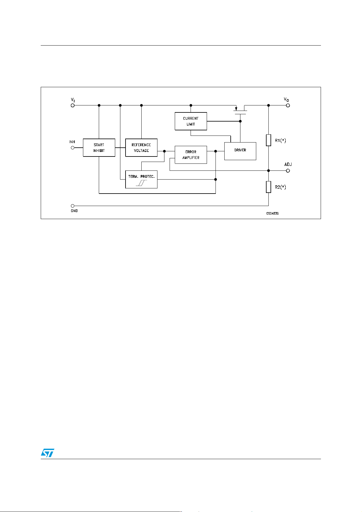
LD39080 Diagram
1 Diagram
Figure 1. Block diagram
(*) Not present on ADJ Versions
3/20
Pin configuration LD39080
2 Pin configuration
Figure 2. Pin connections (top view for DPAK and PPAK, bottom view for DFN8)
DFN8 (4x4 mm)
Table 1. Pin description
Pln N°
Symbol Note
DFN PPAK DPAK
V
85
SENSE
ADJ For adjustable version: Error Amplifier Input pin for V
3, 4 2 1 V
6, 7 4 3 V
21 V
O
INH
1 3 2 GND Common ground
5 N.C. Not Connected
For fixed versions: to be connected with LDO Output Voltage pins for DFN
/N.C.
package and Not Connected on PPAK
LDO Input Voltage; VI from 2.5V to 6V, CI=1µF must be located at a
I
distance of not more than 0.5’’ from input pin.
LDO Output Voltage pins, with minimum CO=2.2µF needed for stability
(also refer to C
Inhibit Input Voltage: ON MODE when V
0.3V (Do not leave floating, not internally pulled down/up)
PPAK
vs. ESR stability chart)
O
DPAK
from 1.22 to 5.0V
O
≥ 2V, OFF MODE when V
INH
INH
≤
4/20
LD39080 Typical application circuits
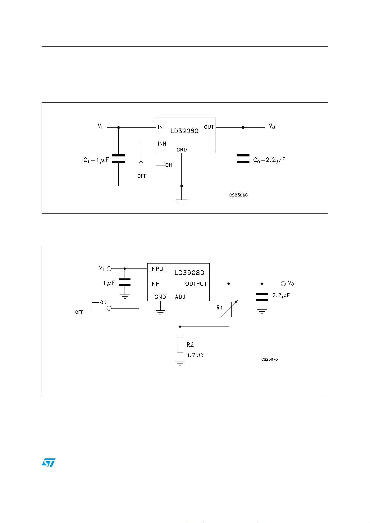
3 Typical application circuits
(CI and CO Capacitors must be placed as close as possible to the IC pins)
Figure 3. LD39080 fixed version with inhibit
1 Inhibit Pin is not internally pulled down/up then it must not be left floating. Disable the device
when connected to GND or to a positive voltage less than 0.3V
Figure 4. LD39080 adjustable version
VO = V
(1 + R1/R2)
REF
2 Set R2 as close as possible to 4.7K
Ω.
5/20
Typical application circuits LD39080
Figure 5. LD39080 DPAK
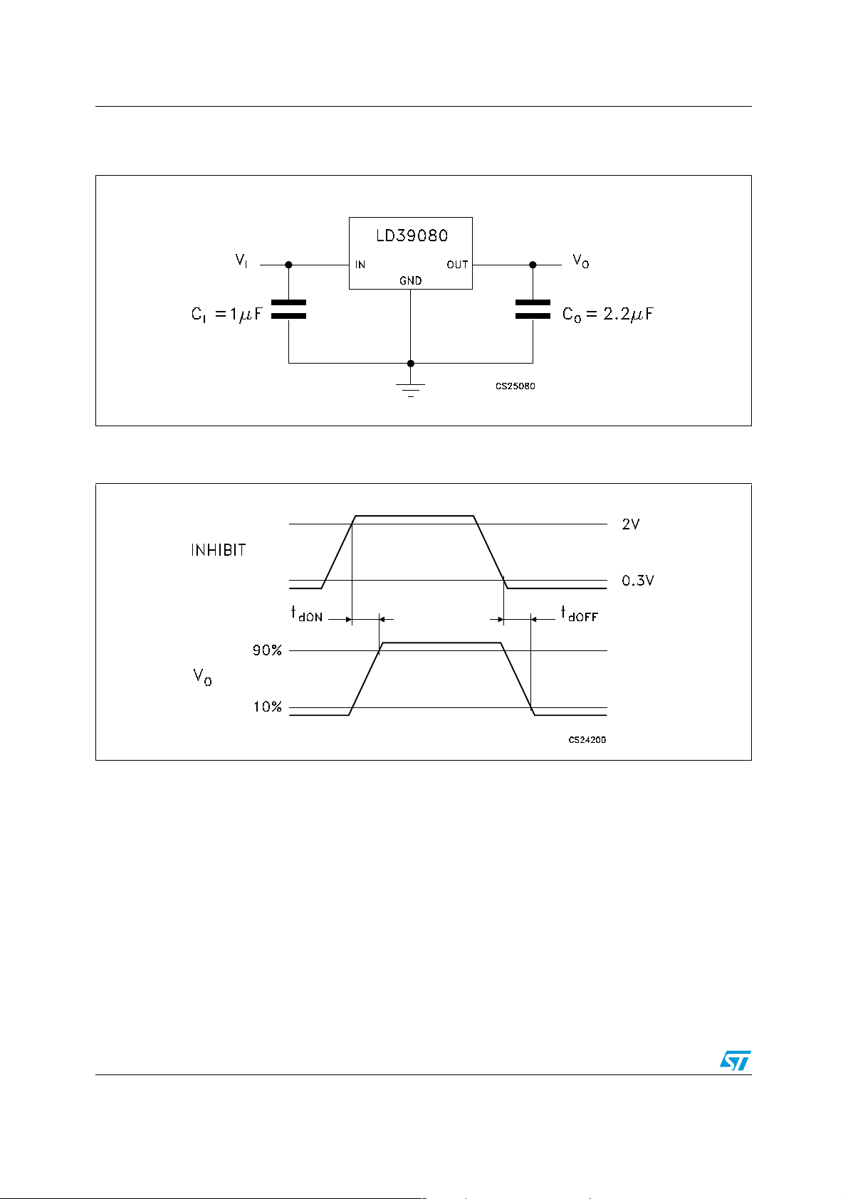
Figure 6. Timing diagram
6/20

LD39080 Maximum ratings
4 Maximum ratings
Table 2. Absolute maximum ratings
Symbol Parameter Value Unit
DC Input voltage -0.3 to 6.5 V
INHIBIT Input voltage -0.3 to VI +0.3 (6.5V Max) V
DC Output voltage -0.3 to VI +0.3 (6.5V Max) V
ADJ Pin voltage -0.3 to VI +0.3 (6.5V Max) V
Output current Internally Limited mA
Power dissipation Internally Limited mW
Storage temperature range -50 to 150 °C
Operating junction temperature range -40 to 125 °C
V
V
T
V
P
STG
T
V
INH
O
ADJ
I
O
D
OP
I
Note: Absolute Maximum Ratings are those values beyond which damage to the device may
occur. Functional operation under these conditions is not implied. All values are referred to
GND.
Table 3. Thermal Data
Symbol Parameter PPAK DPAK DFN
R
thJA
R
thJC
1. With PCB ground plane heatsink.
Thermal resistance junction-ambient 100 100 40 °C/W
Thermal resistance junction-case 8 8 10 °C/W
(1)
Unit
7/20

Electrical characteristics LD39080
5 Electrical characteristics
Table 4. Electrical characteristics
(T
= 25°C, VI = VO+1V, CI = 1µF, CO = 2.2µF, I
J
specified)
Symbol Parameter Parameter Min. Typ. Max. Unit
LOAD
= 10mA, V
= 2V, unless otherwise
INH
Operating input voltage 2.5 6 V
I
Output voltage tolerance
Reference voltage 1.22 V
Output voltage LINE
O
regulation
Output voltage LOAD
LOAD
regulation
Dropout voltage (VI - VO)
V
V
∆V
∆VO/∆I
V
DROP
V
O
REF
Quiescent current:
ON MODE
I
Q
Quiescent current:
OFF MODE
Short Circuit Protection
I
SC
Short circuit protection RL = 0 1.6 A
Inhibit Input
VI = VO+1V, I
= 10mA to 0.8A -1.5 1.5
LOAD
VI = VO+1V to 6V,
I
= 10mA to 0.8A
LOAD
= -40 to 125°C
T
J
= VO+1V to 6V 0.04 %
V
I
V
= VO+1V to 6V, TJ = -40 to 125°C 0.1 0.2 %
I
= 10mA to 0.8A 0.06
I
LOAD
I
= 10mA to 0.8A,
LOAD
= -40 to 125°C
T
J
= 150mA, TJ=-40 to 125°C 20 40
I
LOAD
I
= 0.8A, TJ = -40 to 125°C 150 300
LOAD
I
= 10mA to 0.8A, V
LOAD
= -40 to 125°C
T
J
= 0.3V 1
V
INH
= 0.3V, TJ = -40 to 125°C 5
V
INH
INH
= 2V
-3 3
0.2 0.4
12.5mA
% of
V
O(NOM)
%/A
mV
µA
V
T
D-OFF
T
D-ON
I
INH
INH
Inhibit threshold HIGH 2
Current limit I
Current limit I
Inhibit input current
AC Parameters
SVR Supply voltage rejection
Inhibit threshold LOW
e
N
Output noise voltage
Thermal shutdown OFF 170
T
SHDN
1. Guaranteed by design
Hysteresis 10
8/20
(1)
V
= 2.5 to 6V OFF
I
= -40 to 125°C
T
J
= 0.8A, VO = 3.3V 15
LOAD
= 0.8A, VO = 3.3V 15
LOAD
VI = 6V, V
= 4.5 ± 1V,
V
I
V
= 3.3V,
O
I
LOAD
= 10Hz to 100kHz,
B
W
C
= 2.2µF, VO = 2.5V
O
= 0 to 6V ±0.1 ±1µA
INH
f = 120Hz 65
= 10mA,
f = 1kHz 55
0.3
100 µV
V
µs
dB
RMS
°C

LD39080 Typical performance characteristics
6 Typical performance characteristics
(TJ = 25°C, VI = VO+1V, CI = 1µF, CO = 2.2µF, I
LOAD
= 10mA, V
= VI, unless otherwise
INH
specified)
Figure 7. Output voltage vs temperature Figure 8. Dropout voltage vs temperature
Figure 9. Dropout voltage vs output current Figure 10. Quiescent current vs output current
Figure 11. Quiescent current vs supply
voltage
Figure 12. Quiescent current vs temperature
9/20

Typical performance characteristics LD39080
Figure 13. Quiescent current vs temperature Figure 14. Short circuit current vs temperature
Figure 15. Output voltage vs input voltage Figure 16. Supply voltage rejection vs
temperature
Figure 17. Stability region vs CO & ESR (at
10/20
100kHz)
Figure 18. Stability region vs CO & Low ESR
(at 100kHz)

LD39080 Typical performance characteristics
Figure 19. Load transient Figure 20. Line transient
VI = 3.5V, IO = 10mA to 0.8A, CI = 1µF, CO = 2.2µF
VI = 3.5V to 5.5V, I
= 10mA, CO = 2.2µF
LOAD
11/20

Application notes LD39080
7 Application notes
7.1 External capacitors
The LD39080 requires external capacitors for regulator stability. These capacitors must be
selected to meet the requirements of minimum capacitance and equivalent series resistance
(see
Figure 17. Figure 18.
the relative pins and connected directly to the input/output ground pins using traces which
have no other currents flowing through them. Any good quality of Ceramic or Electrolytic
capacitors can be used.
7.2 Input capacitor
An input capacitor whose minimum value is 1µF is required with the LD39080 (amount of
capacitance can be increased without limit). This capacitor must be located a distance of not
more than 1cm from the input pin of the device and returned to a clean analog ground. Any
good quality ceramic, tantalum or film capacitors can be used for this capacitor.
). The input/output capacitors must be located less than 1cm from
7.3 Output capacitor
It is possible to use Ceramic or Tantalum capacitors but the output capacitor must meet the
requirement for minimum amount of capacitance and E.S.R. (equivalent series resistance)
value. A minimum capacitance of 2.2µF is a good choice to guarantee the stability of the
regulator. Anyway, other C
showing the allowable ESR range as a function of the output capacitance. This curve
represents the stability region over the full temperature and I
values can be used according to the (
O
7.4 Thermal note
The output capacitor must maintain its ESR in the stable region over the full operating
temperature range to assure stability. Also, capacitors tolerance and variation with
temperature must be kept in consideration in order to assure the minimum amount of
capacitance at all times.
7.5 Inhibit input operation
The inhibit pin can be used to turn OFF the regulator when pulled down, so drastically
reducing the current consumption down to less than 1µA. When the inhibit feature is not
used, this pin must be tied to V
proper operation, the signal source used to drive the inhibit pin must be able to swing above
and below the specified thresholds listed in the electrical characteristics section (V
The inhibit pin must not be left floating because it is not internally pulled down/up.
to keep the regulator output ON at all times. To assure
I
Figure 17. Figure 18.
range.
O
IH VIL
)
).
12/20

LD39080 Package mechanical data
8 Package mechanical data
In order to meet environmental requirements, ST offers these devices in ECOPACK®
packages. These packages have a Lead-free second level interconnect. The category of
second Level Interconnect is marked on the package and on the inner box label, in
compliance with JEDEC Standard JESD97. The maximum ratings related to soldering
conditions are also marked on the inner box label. ECOPACK is an ST trademark.
ECOPACK specifications are available at: www.st.com.
13/20

Package mechanical data LD39080
PPAK MECHANICAL DATA
DIM.
MIN. TYP MAX. MIN. TYP. MAX.
A 2.2 2.4 0.086 0.094
A1 0.9 1.1 0.035 0.043
A2 0.03 0.23 0.001 0.009
B 0.4 0.6 0.015 0.023
B2 5.2 5.4 0.204 0.212
C 0.45 0.6 0.017 0.023
C2 0.48 0.6 0.019 0.023
D 6 6.2 0.236 0.244
D1 5.1 0.201
E 6.4 6.6 0.252 0.260
E1 4.7 0.185
e 1.27 0.050
G 4.9 5.25 0.193 0.206
G1 2.38 2.7 0.093 0.106
H 9.35 10.1 0.368 0.397
L2 0.8 1 0.031
L4 0.6 1 0.023 0.039
L5 1
L6 2.8 0.110
mm. inch
0.039
0.039
14/20
0078180-E

LD39080 Package mechanical data
DPAK MECHANICAL DATA
DIM.
MIN. TYP MAX. MIN. TYP. MAX.
A 2.2 2.4 0.086 0.094
A1 0.9 1.1 0.035 0.043
A2 0.03 0.23 0.001 0.009
B 0.64 0.9 0.025 0.035
b4 5.2 5.4 0.204 0.212
C 0.45 0.6 0.017 0.023
C2 0.48 0.6 0.019 0.023
D 6 6.2 0.236 0.244
D1 5.1 0.200
E 6.4 6.6 0.252 0.260
E1 4.7 0.185
e 2.28 0.090
e1 4.4 4.6 0.173 0.181
H 9.35 10.1 0.368 0.397
L 1 0.039
(L1)
L2 0.8 0.031
L4 0.6 1 0.023 0.039
mm. inch
2.8 0.110
0068772-F
15/20

Package mechanical data LD39080
DFN8 (4x4) MECHANICAL DATA
mm. inch
DIM.
MIN. TYP MAX. MIN. TYP. MAX.
A 0.80 0.90 1.00 0.031 0.035 0.039
A1 0 0.02 0.05 0 0.001 0.002
A3 0.20 0.008
b 0.23 0.30 0.38 0.009 0.012 0.015
D3.90 4.00 4.10 0.154 0.157 0.161
D2 2.82 3.00 3.23 0.111 0.118 0.127
E3.90 4.00 4.10 0.154 0.157 0.161
E2 2.05 2.20 2.30 0.081 0.087 0.091
e 0.80 0.031
L 0.40 0.50 0.60 0.016 0.020 0.024
16/20
7869653B

LD39080 Package mechanical data
Tape & Reel DPAK-PPAK MECHANICAL DATA
DIM.
MIN. TYP MAX. MIN. TYP. MAX.
A 330 12.992
C 12.8 13.0 13.2 0.504 0.512 0.519
D 20.2 0.795
N 60 2.362
T 22.4 0.882
Ao 6.80 6.90 7.00 0.268 0.272 0.2.76
Bo 10.40 10.50 10.60 0.409 0.413 0.417
Ko 2.55 2.65 2.75 0.100 0.104 0.105
Po 3.9 4.0 4.1 0.153 0.157 0.161
P 7.9 8.0 8.1 0.311 0.315 0.319
mm. inch
17/20

Package mechanical data LD39080
Tape & Reel QFNxx/DFNxx (4x4) MECHANICAL DATA
mm. inch
DIM.
MIN. TYP MAX. MIN. TYP. MAX.
A 330 12.992
C 12.8 13.2 0.504 0.519
D 20.2 0.795
N 99 101 3.898 3.976
T 14.4 0.567
Ao 4.35 0.171
Bo 4.35 0.171
Ko 1.1 0.043
Po 4 0.157
P 8 0.315
18/20

LD39080 Revision history
9 Revision history
Table 5. Revision history
Date Revision Changes
26-Jan-2007 1 Initial release.
19/20

LD39080
Please Read Carefully:
Information in this document is provided solely in connection with ST products. STMicroelectronics NV and its subsidiaries (“ST”) reserve the
right to make changes, corrections, modifications or improvements, to this document, and the products and services described herein at any
time, without notice.
All ST products are sold pursuant to ST’s terms and conditions of sale.
Purchasers are solely responsible for the choice, selection and use of the ST products and services described herein, and ST assumes no
liability whatsoever relating to the choice, selection or use of the ST products and services described herein.
No license, express or implied, by estoppel or otherwise, to any intellectual property rights is granted under this document. If any part of this
document refers to any third party products or services it shall not be deemed a license grant by ST for the use of such third party products
or services, or any intellectual property contained therein or considered as a warranty covering the use in any manner whatsoever of such
third party products or services or any intellectual property contained therein.
UNLESS OTHERWISE SET FORTH IN ST’S TERMS AND CONDITIONS OF SALE ST DISCLAIMS ANY EXPRESS OR IMPLIED
WARRANTY WITH RESPECT TO THE USE AND/OR SALE OF ST PRODUCTS INCLUDING WITHOUT LIMITATION IMPLIED
WARRANTIES OF MERCHANTABILITY, FITNESS FOR A PARTICULAR PURPOSE (AND THEIR EQUIVALENTS UNDER THE LAWS
OF ANY JURISDICTION), OR INFRINGEMENT OF ANY PATENT, COPYRIGHT OR OTHER INTELLECTUAL PROPERTY RIGHT.
UNLESS EXPRESSLY APPROVED IN WRITING BY AN AUTHORIZED ST REPRESENTATIVE, ST PRODUCTS ARE NOT
RECOMMENDED, AUTHORIZED OR WARRANTED FOR USE IN MILITARY, AIR CRAFT, SPACE, LIFE SAVING, OR LIFE SUSTAINING
APPLICATIONS, NOR IN PRODUCTS OR SYSTEMS WHERE FAILURE OR MALFUNCTION MAY RESULT IN PERSONAL INJURY,
DEATH, OR SEVERE PROPERTY OR ENVIRONMENTAL DAMAGE. ST PRODUCTS WHICH ARE NOT SPECIFIED AS "AUTOMOTIVE
GRADE" MAY ONLY BE USED IN AUTOMOTIVE APPLICATIONS AT USER’S OWN RISK.
Resale of ST products with provisions different from the statements and/or technical features set forth in this document shall immediately void
any warranty granted by ST for the ST product or service described herein and shall not create or extend in any manner whatsoever, any
liability of ST.
ST and the ST logo are trademarks or registered trademarks of ST in various countries.
Information in this document supersedes and replaces all information previously supplied.
The ST logo is a registered trademark of STMicroelectronics. All other names are the property of their respective owners.
© 2007 STMicroelectronics - All rights reserved
STMicroelectronics group of companies
Australia - Belgium - Brazil - Canada - China - Czech Republic - Finland - France - Germany - Hong Kong - India - Israel - Italy - Japan -
Malaysia - Malta - Morocco - Singapore - Spain - Sweden - Switzerland - United Kingdom - United States of America
www.st.com
20/20
 Loading...