


ST LD39050PU105R, LD39050PU15R, LD39050PU18R User Manual
Features
■ Input voltage from 1.5 to 5.5 V
■ Ultra low dropout voltage (200 mV typ. at 500
mA load)
■ Very low quiescent current (20 µA typ. at no
load, 100 µA typ. at 500 mA load, 1 µA max in
off mode)
■ Very low noise without bypass capacitor
■ Output voltage tolerance: ± 2.0 % @ 25 °C
■ 500 mA guaranteed output current
■ Wide range of output voltages available on
request: 0.8 V to 4.5 V with 100 mV step and
ADJ from 0.8 V
■ Logic-controlled electronic shutdown
■ Compatible with ceramic capacitor
C
= 1 µF
OUT
■ Internal current and thermal limit
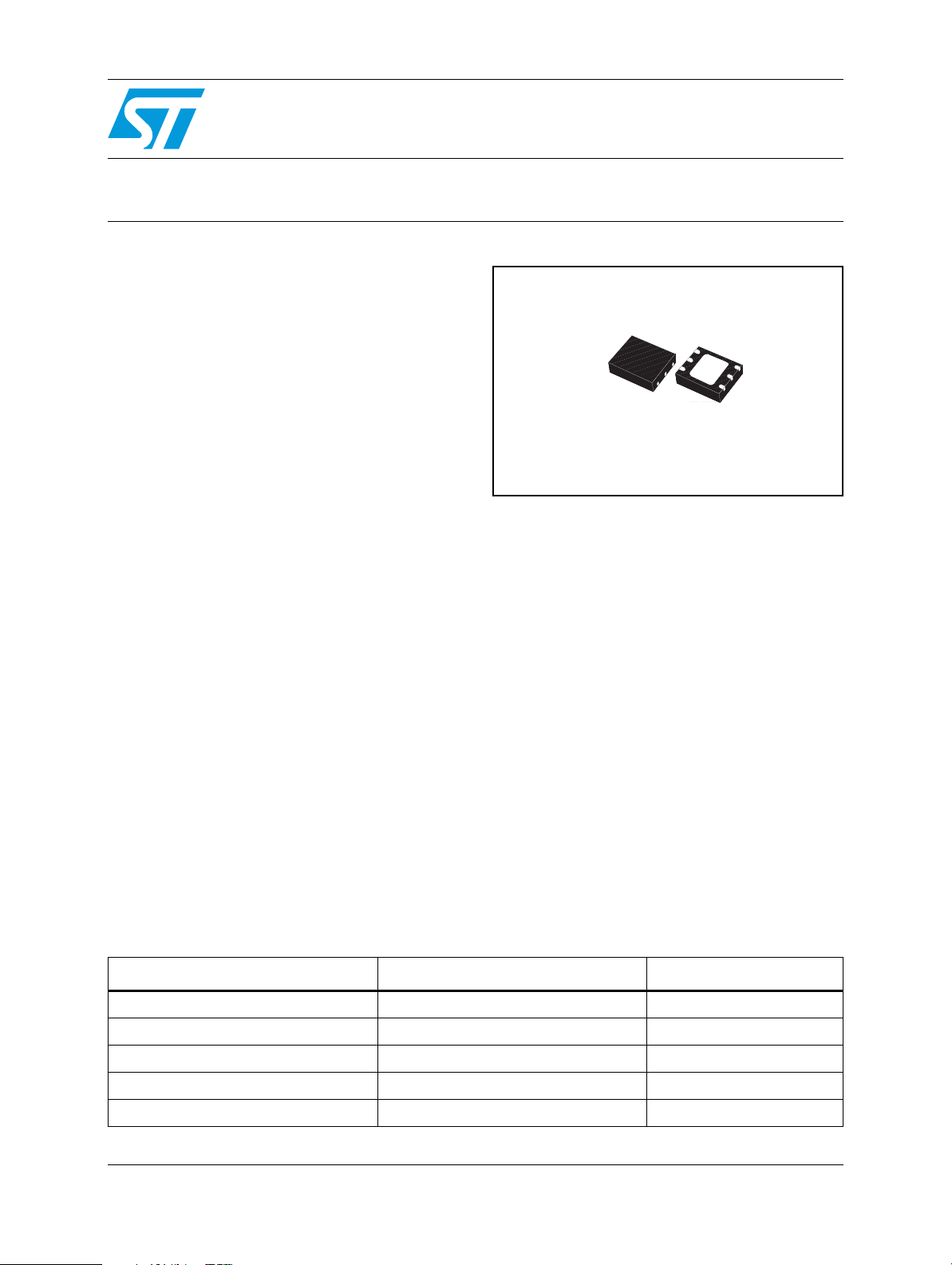
■ Package DFN6 (3 x 3 mm)
■ Temperature range: -40 °C to 125 °C
LD39050xx
500 mA low quiescent current
low noise voltage regulator
DFN6 (3 x 3 mm)
roll off at 10 kHz. An Enable logic control function
puts the LD39050 in shut-down mode allowing a
total current consumption lower than 1 µA. The
device also includes short-circuit constant current
limiting and thermal protection. Typical
applications are mobile phones, personal digital
assistants (PDAs), cordless phones and similar
battery-powered systems.
Description
The LD39050 provides 500 mA maximum current
from an input voltage ranging from 1.5 V to 5.5 V
with a typical dropout voltage of 200 mV. Stability
is provided using ceramic capacitors. The ultra
low drop-voltage, low quiescent current and low
noise features make it suitable for low power
battery-powered applications. Power supply
rejection is 65 dB at low frequencies and starts to
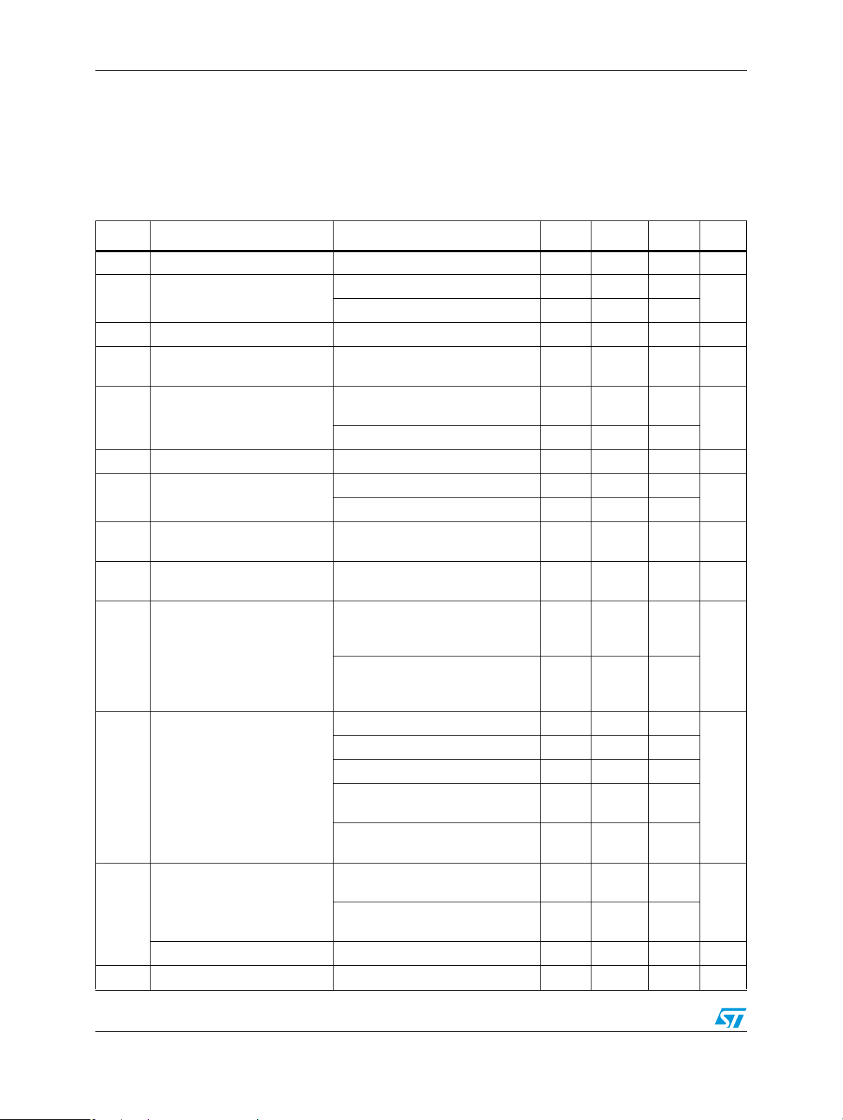
Table 1. Device summary
Part numbers Order codes Output voltages
LD39050XX LD39050PUR ADJ from 0.8 V
LD39050XX10 LD39050PU10R 1.0 V
LD39050XX12 LD39050PU12R 1.2 V
LD39050XX25 LD39050PU25R 2.5 V
LD39050XX33 LD39050PU33R 3.3 V
March 2009 Rev 1 1/24
www.st.com
24

Contents LD39050xx
Contents
1 Diagrams . . . . . . . . . . . . . . . . . . . . . . . . . . . . . . . . . . . . . . . . . . . . . . . . . . 3
2 Pin configuration . . . . . . . . . . . . . . . . . . . . . . . . . . . . . . . . . . . . . . . . . . . 4
3 Maximum ratings . . . . . . . . . . . . . . . . . . . . . . . . . . . . . . . . . . . . . . . . . . . . 5
4 Electrical characteristics . . . . . . . . . . . . . . . . . . . . . . . . . . . . . . . . . . . . . 6
5 Typical performance characteristics . . . . . . . . . . . . . . . . . . . . . . . . . . . 10
6 Application information . . . . . . . . . . . . . . . . . . . . . . . . . . . . . . . . . . . . . 15
6.1 Power dissipation . . . . . . . . . . . . . . . . . . . . . . . . . . . . . . . . . . . . . . . . . . . 16
6.2 Enable function . . . . . . . . . . . . . . . . . . . . . . . . . . . . . . . . . . . . . . . . . . . . . 16
6.3 Power Good function . . . . . . . . . . . . . . . . . . . . . . . . . . . . . . . . . . . . . . . . 16
7 Package mechanical data . . . . . . . . . . . . . . . . . . . . . . . . . . . . . . . . . . . . 18
8 Different output voltage versions of the LD39050xx
available on request . . . . . . . . . . . . . . . . . . . . . . . . . . . . . . . . . . . . . . . . 22
9 Revision history . . . . . . . . . . . . . . . . . . . . . . . . . . . . . . . . . . . . . . . . . . . 23
2/24
LD39050xx Diagrams
1 Diagrams
Figure 1. Schematic diagram for the LD39050PU
IN
IN
BandGap
BandGap
reference
reference
OpAmp
OpAmp
EN
EN
Figure 2. Schematic diagram for the LD39050PUxx
Internal
Internal
enable
enable
GND
GND
Power-good
Power-good
Current
Current
limit
limit
Thermal
Thermal
protection
protection
signal
signal
PG
PG
IN
ININ
OUT
OUT
ADJ
ADJ
IN
IN
EN
EN
BandGap
BandGap
reference
reference
Internal
Internal
enable
enable
OpAmp
OpAmp
GND
GND
Power-good
Power-good
Current
Current
limit
limit
Thermal
Thermal
protection
protection
signal
signal
PG
PG
IN
ININ
OUT
OUT
R
R
1
1
NC
NC
R
R
2
2
3/24
Pin configuration LD39050xx
2 Pin configuration
Figure 3. Pin connection (top view)
EN
GND
PG
LD39050PUxx
V
NC
V
IN
OUT
EN
GND
PG
LD39050PU
Table 2. Pin description
Pin n°
Symbol
LD39050PU LD39050PUxx
EN 1 1 Enable pin logic input: Low=shutdown, High=active
GND 2 2 Common ground
PG 3 3 Power Good
V
OUT
4 4 Output voltage
ADJ 5 - Adjust pin
V
IN
6 6 Input voltage of the LDO
NC - 5 Not connected
GND EXP pad Exposed pad must be connected to GND
Function
V
IN
ADJ
V
OUT
4/24
LD39050xx Maximum ratings
3 Maximum ratings
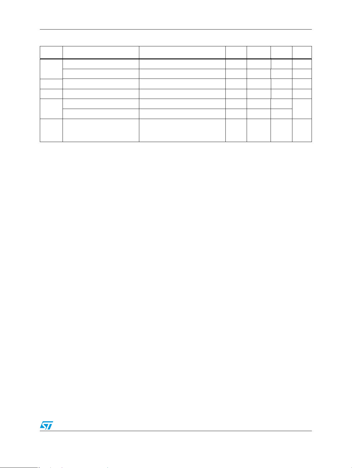
Table 3. Absolute maximum ratings
Symbol Parameter Value Unit
V
IN
V
OUT
EN Enable pin -0.3 to V
DC input voltage -0.3 to 7 V
DC output voltage -0.3 to VI + 0.3 (7 V max) V
+ 0.3 (7 V max) V
I
PG Power Good pin -0.3 to 7 V
ADJ Adjust pin 4 V
I
T
T
OUT
P
D
STG
OP
Output current Internally limited
Power dissipation Internally limited
Storage temperature range - 65 to 150 °C
Operating junction temperature range - 40 to 125 °C
Note: Absolute maximum ratings are those values beyond which damage to the device may occur.
Functional operation under these conditions is not implied. All values are referred to GND.
Table 4. Thermal data
Symbol Parameter Value Unit
R
R
thJA
thJC
Thermal resistance junction-ambient 55 °C/W
Thermal resistance junction-case 10 °C/W
Table 5. ESD performance
Symbol Parameter Test conditions Value Unit
HBM 2 kV
ESD ESD protection voltage
MM 0.3 kV
5/24
Electrical characteristics LD39050xx
4 Electrical characteristics
TJ = 25 °C, V
= 1.8 V, CIN = C
IN
OUT
= 1 µF, I
= 10 mA, VEN = VIN, unless otherwise
OUT
specified.
Table 6. Electrical characteristics for the LD39050PU
Symbol Parameter Test conditions Min. Typ. Max. Unit
V
IN
V
ADJVADJ
I
ADJ
ΔV
OUT
ΔV
OUT
ΔV
OUT
ΔV
OUT
V
DROP
Operating input voltage 1.5 5.5 V
I
=10 mA, TJ = 25°C 784 800 816
accuracy
OUT
= 10 mA, -40°C<TJ<125°C 776 800 824
I
OUT
mV
Adjust pin current 1µA
+1 V ≤ VIN ≤ 5.5 V,
V
Static line regulation
Transient line regulation
(1)
Static load regulation I
Transient load regulation
Dropout voltage
(2)
(1)
OUT
= 1 mA
I
OUT
ΔVIN=500 mV, I
=10 mA, tR=5
OUT
µs
ΔV
=500 mV, I
IN
= 10 mA to 500 mA 0.002 %/mA
OUT
I
= 10 mA to 500 mA, tR=5µs 40
OUT
= 10 mA to 500 mA, tF=5µs 40
I
OUT
IO = 500mA, V
=10 mA, tF=5 µs 10
OUT
fixed to 1.5V
OUT
40°C<TJ<125°C
0.01 %/V
10
200 400 mV
mVpp
mVpp
e
N
SVR
I
Q
PG
I
SC
Output noise voltage
Supply voltage rejection
= 0.8V
V
OUT
Quiescent current
Power Good output threshold
10Hz to 100kHz, I
V
= 0.8 V
OUT
VIN = 1.8V+/-V
V
I
V
V
I
I
I
I
I
40°C<T
V
V
= 0.25V, freq. = 1kHz
RIPPLE
= 10 mA
OUT
= 1.8V+/-V
IN
= 0.25V, freq.=10 kHz
RIPPLE
= 100 mA
OUT
= 0 mA 20
OUT
= 0 mA, -40°C<TJ<125°C 50
OUT
= 0 to 500mA 100
OUT
=0 to 500mA, -
OUT
<125°C
J
input current in off mode:
IN
EN
= GND
(3)
Rising edge
Falling edge
OUT
RIPPLE
RIPPLE
= 100 mA,
30 µV
65
62
200
0.001 1
0.92*
V
OUT
0.8*
V
OUT
RMS
dB
µA
V
Power Good output voltage low Isink=6mA open drain output 0.4 V
Short-circuit current RL=0 600 800 mA
6/24
LD39050xx Electrical characteristics
Table 6. Electrical characteristics for the LD39050PU (continued)
Symbol Parameter Test conditions Min. Typ. Max. Unit
V
EN
Enable input logic high V
I
Enable pin input current VEN= V
EN
t
ON
Turn on time
(4)
=1.5 V to 5.5 V, 40°C<TJ<125°C 0.9 V
IN
IN
0.1 100 nA
30 µs
Thermal shutdown 160
Enable input logic low VIN=1.5 V to 5.5 V, 40°C<TJ<125°C 0.4 V
T
SHDN
Hysteresis 20
°C
Capacitance (see typical
C
Output capacitor
OUT
performance characteristics for
122µF
stability)
1. All transient values are guaranteed by design, not production tested
2. Dropout voltage is the input-to-output voltage difference at which the output voltage is 100 mV below its nominal value. This
specification does not apply for output voltages below 1.5 V
3. PG pin floating
4. Turn-on time is time measured between the enable input just exceeding V
reaching 95% of its nominal value
high value and the output voltage just
EN
7/24
Electrical characteristics LD39050xx
TJ = 25 °C, V
IN
= V
OUT(NOM)
+ 1 V, CIN = C
OUT
= 1 µF, I
= 10 mA, VEN = VIN, unless
OUT
otherwise specified.
Table 7. Electrical characteristics for the LD39050PUxx
Symbol Parameter Test conditions Min. Typ. Max. Unit
V
IN
V
OUTVOUT
ΔV
OUT
ΔV
OUT
ΔV
OUT
ΔV
OUT
V
DROP
Operating input voltage 1.5 5.5 V
V
accuracy
Static line regulation
Transient line regulation
(1)
Static load regulation I
Transient load regulation
Dropout voltage
(2)
(1)
>1.5V, I
OUT
= 25°C
T
J
>1.5 V, I
V
OUT
-40°C<T
V
OUT
V
OUT
-40°C<T
V
OUT
I
OUT
<125°C
J
≤ 1.5 V, I
≤ 1.5 V, I
<125°C
J
+1 V ≤ VIN ≤ 5.5 V,
= 1 mA
ΔVIN=500 mV, I
=500 mV, I
ΔV
IN
= 10 mA to 500 mA 0.002 %/mA
OUT
I
= 10 mA to 500 mA, tR=5µs 40
OUT
= 10 mA to 500 mA, tF=5µs 40
I
OUT
I
= 500mA, V
OUT
-40°C<TJ<125°C
=10 mA,
OUT
= 10 mA,
OUT
= 10 mA ±20
OUT
=10 mA,
OUT
=10 mA, tR=5 µs 10
OUT
=10 mA, tF=5 µs 10
OUT
> 1.5 V
OUT
-2.0 2.0
-3.0 3.0
±30
mV
0.01 %/V
mVpp
mVpp
200 400 mV
%
e
N
SVR
I
Q
PG
I
SC
Output noise voltage 10Hz to 100kHz, IO = 100 mA, 30 µV
Supply voltage rejection
V
= 1.5V
OUT
Quiescent current
Power Good output threshold
Power Good output voltage
low
VIN = V
OUT(NOM
V
I
V
V
I
I
I
I
I
V
V
= 0.1V, freq. = 1kHz
RIPPLE
= 10 mA
OUT
= V
IN
OUT(NOM)
= 0.1V, freq.=10 kHz
RIPPLE
= 100 mA
OUT
= 0 mA 20
OUT
= 0 mA, -40°C<TJ<125°C 50
OUT
= 0 to 500mA 100
OUT
= 0 to 500mA -40°C<TJ<125°C 200
OUT
input current in off mode:
IN
= GND
EN
Rising edge
Falling edge
Isink=6mA open drain output 0.4 V
)+0.5V+/-V
+0.5V+/-V
(3)
RIPPLE
RIPPLE
65
62
0.001 1
0.92*
V
OUT
0.8*
V
OUT
RMS
dB
µA
V
Short-circuit current RL=0 600 800 mA
8/24