

Features
■ Input voltage from 1.5 to 5.5 V
■ Ultra low dropout voltage (80 mV typ. at 100
mA load)
■ Very low quiescent current (18 µA typ. at no
load, 35 µA typ. at 150 mA load, 1 µA max in off
mode)
■ Very low noise without bypass capacitor
(29 µV
■ Output voltage tolerance: ± 2.0% @ 25 °C
■ 150 mA guaranteed output current
■ Wide range of output voltages available on
RMS
at V
OUT
= 0.8 V)
request: 0.8 V to 3.3 V with 100 mV step
■ Logic-controlled electronic shutdown
■ Compatible with ceramic capacitors C
■ Internal current and thermal limit
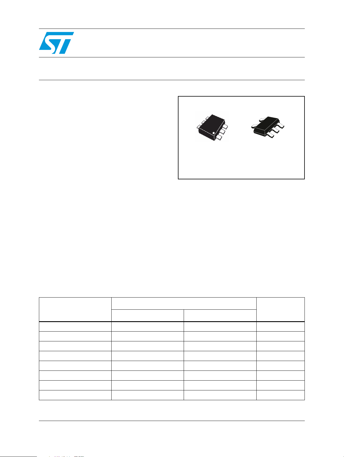
■ Available in SOT666 and SOT23-5L packages
■ Temperature range: -40 °C to 125 °C
= 1 µF
O
Description
The LD39015xx series provides 150 mA
maximum current from an input voltage ranging
Table 1. Device summary
LD39015xx
150 mA low quiescent current
low noise voltage regulator
SOT666
from 1.5 V to 5.5 V with a typical dropout voltage
of 80 mV. It is stable with ceramic capacitor. The
ultra-low drop voltage, low quiescent current and
low noise features make it suitable for low power
battery-powered applications. Power supply
rejection is 65 dB at low frequencies and starts to
roll off at 10 kHz. Enable logic control function
puts the LD39015xx in shut-down mode allowing
a total current consumption lower than 1 µA. The
device also includes short-circuit constant current
limiting and thermal protection. Typical
applications are mobile phones, personal digital
assistants (PDAs), cordless phones or similar
battery-powered systems.
SOT23-5L
Order codes
Part numbers
SOT666 SOT23-5L
LD39015XX08 LD39015XG08R LD39015M08R 0.8 V
LD39015XX10 LD39015XG10R
LD39015XX12 LD39015XG12R LD39015M12R 1.2 V
LD39015XX125 LD39015M125R 1.25 V
LD39015XX15 LD39015XG15R
LD39015XX18 LD39015XG18R
LD39015XX25 LD39015XG25R
LD39015XX33 LD39015XG33R LD39015M33R 3.3 V
1. Available on request. Other voltages available on request from 0.8 V to 3.3 V in 100 mV step.
February 2009 Rev 3 1/16
(1)
(1)
(1)
(1)
LD39015M10R 1.0 V
LD39015M15R 1.5 V
LD39015M18R 1.8 V
LD39015M25R 2.5 V
Output voltages
www.st.com
16

Contents LD39015xx
Contents
1 Diagram . . . . . . . . . . . . . . . . . . . . . . . . . . . . . . . . . . . . . . . . . . . . . . . . . . . 3
2 Pin configuration . . . . . . . . . . . . . . . . . . . . . . . . . . . . . . . . . . . . . . . . . . . 4
3 Typical application . . . . . . . . . . . . . . . . . . . . . . . . . . . . . . . . . . . . . . . . . . 5
4 Maximum ratings . . . . . . . . . . . . . . . . . . . . . . . . . . . . . . . . . . . . . . . . . . . . 6
5 Electrical characteristics . . . . . . . . . . . . . . . . . . . . . . . . . . . . . . . . . . . . . 7
6 Typical performance characteristics . . . . . . . . . . . . . . . . . . . . . . . . . . . . 9
7 Package mechanical data . . . . . . . . . . . . . . . . . . . . . . . . . . . . . . . . . . . . 11
8 Revision history . . . . . . . . . . . . . . . . . . . . . . . . . . . . . . . . . . . . . . . . . . . 15
2/16
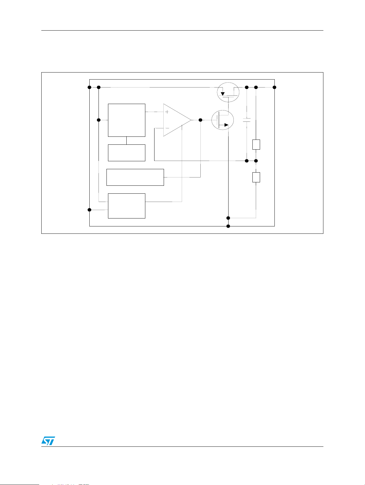
LD39015xx Diagram
1 Diagram
Figure 1. Block diagram
OUT
IN
IN
BandGap
BandGap
1.22 V
1.22 V
Trimming
Trimming
Thermal
Thermal
Protection
Protection
OUT
R1
R1
R2
R2
EN
EN
Enable
Enable
GND
GND
3/16
Pin configuration LD39015xx
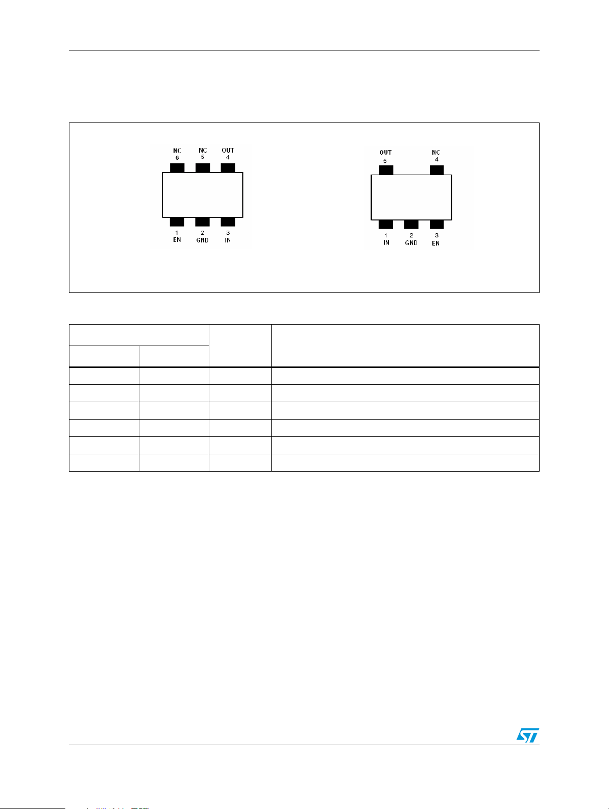
2 Pin configuration
Figure 2. Pin connection (top view)
SOT666
Table 2. Pin description
Pin n°
SOT666 SOT23-5L
1 3 EN Enable pin logic input: Low=shutdown, High=active
2 2 GND Common ground.
3 1 IN Input voltage of the LDO
4 5 OUT Output voltage
5 4 NC Not connected
6 NC Not connected
SOT23-5L
Symbol Function
4/16
LD39015xx Typical application
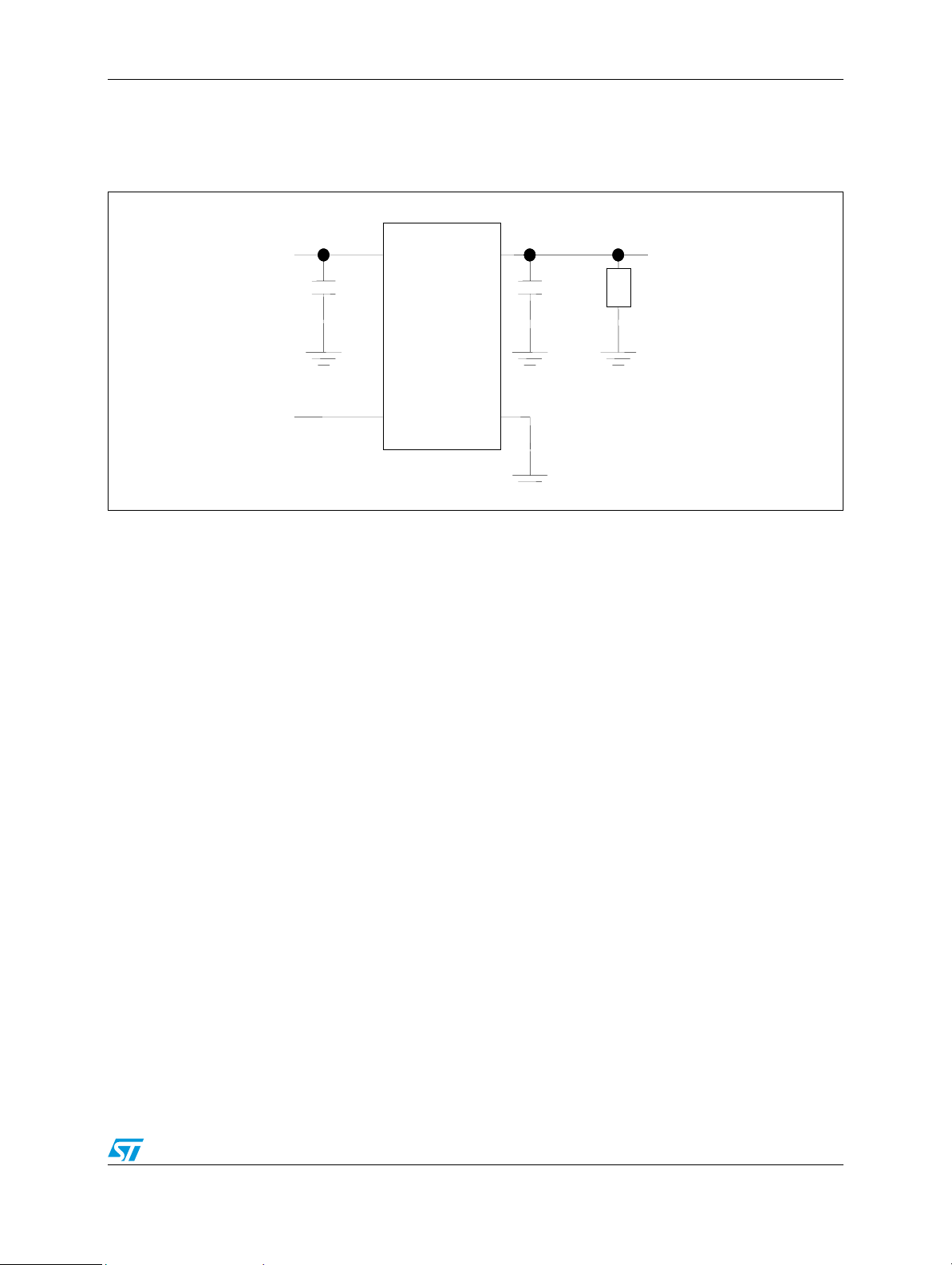
3 Typical application
Figure 3. Typical application circuit
V
V
V
IN
IN
IN
IN
OUT
OUT
V
OUT
OUT
1 µF
1 µF
V
V
EN
EN
EN
EN
GND
GND
1 µF
1 µF
Load
Load
5/16
 Loading...