

ST LD2981ABM25TR, LD2981ABU25TR, LD2981CU25TR, LD2981ABM30TR, LD2981ABU30TR User Manual
...
Ultra low drop voltage regulators with inhibit
low ESR output capacitors compatible
Features
■ Stable with low ESR ceramic capacitors
■ Ultra low dropout voltage (0.17 V typ. at 100
mA load, 7 mV typ. at 1 mA load)
■ Very low quiescent current (80 µA typ. at no
load in on mode; max 1 µA in off mode)
■ Guaranteed output current up to 100mA
■ Logic-controlled electronic shutdown
■ Output voltage of 2.5; 3.0; 3.3; 5.0 V
■ Internal current and thermal limit
■ ± 0.75 % tolerance output voltage available (A
version)
■ Output low noise voltage 160 µV
■
Temperature range: -40 to 125 °C
■ Smallest package SOT23-5L and SOT-89
■ Fast dynamic response to line and load
changes
RMS
LD2981ABxx
LD2981Cxx
SOT-89SOT23-5L
logic control function is available on pin n° 3 (TTL
compatible). This means that when thedevice is
used as local regulator, it is possible to put a part
of the board in standby, decreasing the total
power consumption. The LD2981AB/C is
designed to work with low ESR ceramic capacitor.
Typical applications are in cellular phone,
palmtop/laptop computer, personal digital
assistant (PDA), personal stereo, camcorder and
camera.
Description
The LD2981AB/C series are 100 mA fixed-output
voltage regulator. The low drop-voltage and the
ultra low quiescent current make them suitable for
low noise, low power applications and in battery
powered systems.
The quiescent current in sleep mode is less than
1 µA when INHIBIT pin is pulled low. Shutdown
Table 1. Device summary
Part numbers
Output voltage
AB Versio n C Vers ion
LD2981ABXX25 LD2981CXX25 2.5 V
LD2981ABXX30 LD2981CXX30 3.0 V
LD2981ABXX33 LD2981CXX33 3.3 V
LD2981ABXX50 LD2981CXX50 5.0 V
July 2008 Rev 14 1/23
www.st.com
23

LD2981ABxx - LD2981Cxx
Contents
1 Diagram . . . . . . . . . . . . . . . . . . . . . . . . . . . . . . . . . . . . . . . . . . . . . . . . . . . 3
2 Pin configuration . . . . . . . . . . . . . . . . . . . . . . . . . . . . . . . . . . . . . . . . . . . 4
3 Maximum ratings . . . . . . . . . . . . . . . . . . . . . . . . . . . . . . . . . . . . . . . . . . . . 5
4 Typical application . . . . . . . . . . . . . . . . . . . . . . . . . . . . . . . . . . . . . . . . . . 6
5 Electrical characteristics . . . . . . . . . . . . . . . . . . . . . . . . . . . . . . . . . . . . . 7
6 Typical performance characteristics . . . . . . . . . . . . . . . . . . . . . . . . . . . 11
7 Application notes . . . . . . . . . . . . . . . . . . . . . . . . . . . . . . . . . . . . . . . . . . 14
7.1 External capacitors . . . . . . . . . . . . . . . . . . . . . . . . . . . . . . . . . . . . . . . . . . 14
7.2 Input capacitor . . . . . . . . . . . . . . . . . . . . . . . . . . . . . . . . . . . . . . . . . . . . . 14
7.3 Output capacitor . . . . . . . . . . . . . . . . . . . . . . . . . . . . . . . . . . . . . . . . . . . . 14
7.4 Important . . . . . . . . . . . . . . . . . . . . . . . . . . . . . . . . . . . . . . . . . . . . . . . . . 14
7.5 Inhibit input operation . . . . . . . . . . . . . . . . . . . . . . . . . . . . . . . . . . . . . . . . 14
7.6 Reverse current . . . . . . . . . . . . . . . . . . . . . . . . . . . . . . . . . . . . . . . . . . . . 15
8 Package mechanical data . . . . . . . . . . . . . . . . . . . . . . . . . . . . . . . . . . . . 16
9 Order codes . . . . . . . . . . . . . . . . . . . . . . . . . . . . . . . . . . . . . . . . . . . . . . . 21
10 Revision history . . . . . . . . . . . . . . . . . . . . . . . . . . . . . . . . . . . . . . . . . . . 22
2/23
LD2981ABxx - LD2981Cxx Diagram
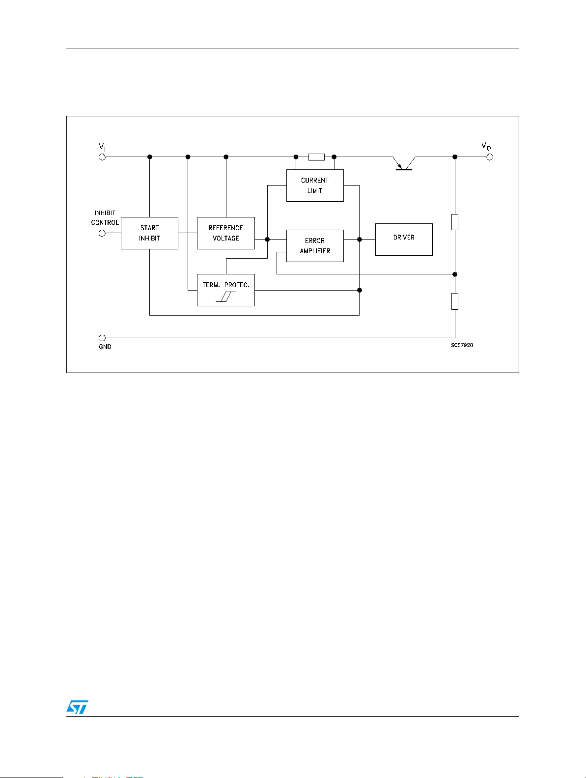
1 Diagram
Figure 1. Schematic diagram
3/23
Pin configuration LD2981ABxx - LD2981Cxx
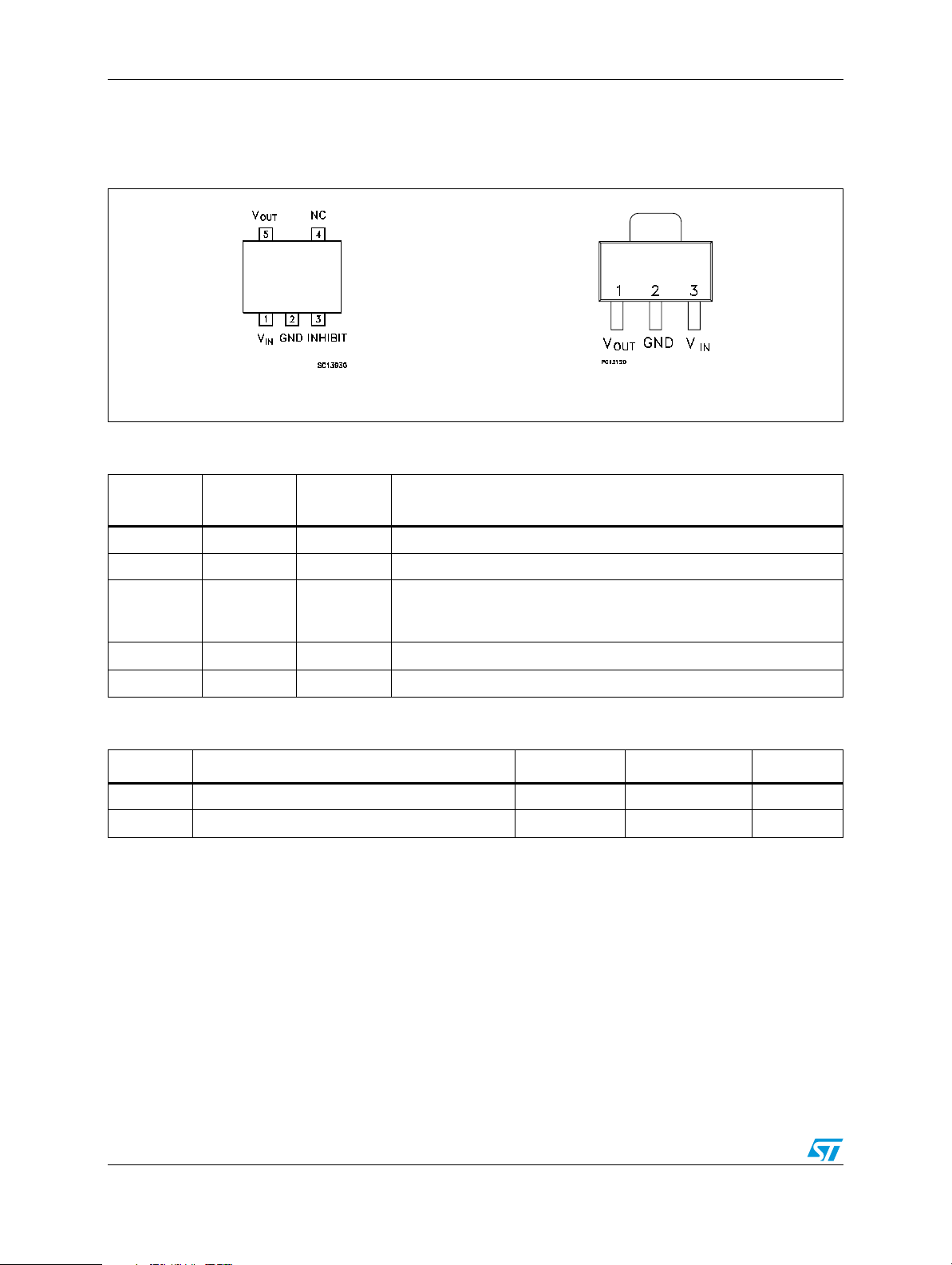
2 Pin configuration
Figure 2. Pin connections (top view)
SOT23-5L
SOT-89
Table 2. Pin description
Pin n°
SOT23-5L
13V
2 2 GND Ground pin
3INHIBIT
4 NC Not connected
51V
Pin n°
SOT-89
Symbol Name and function
IN
Input port
Control switch ON/OFF. Inhibit is not internally pulled-up; it cannot be
left floating. Disable the device when connected to GND or to a
positive voltage less than 0.18 V
OUT
Output port
Table 3. Thermal data
Symbol Parameter SOT23-5L SOT-89 Unit
R
R
thJC
thJA
Thermal resistance junction-case 81 15 °C/W
Thermal resistance junction-ambient 255 110 °C/W
4/23
LD2981ABxx - LD2981Cxx Maximum ratings
3 Maximum ratings
Table 4. Absolute maximum ratings
Symbol Parameter Value Unit
T
V
T
V
INH
I
O
P
STG
OP
I
D
DC input voltage -0.3 to 16 V
INHIBIT input voltage -0.3 to 16 V
Output current Internally limited
Power dissipation Internally limited
Storage temperature range -55 to 150 °C
Operating junction temperature range -40 to 125 °C
Note: Absolute maximum ratings are those values beyond which damage to the device may occur.
Functional operation under these condition is not implied.
5/23
Typical application LD2981ABxx - LD2981Cxx
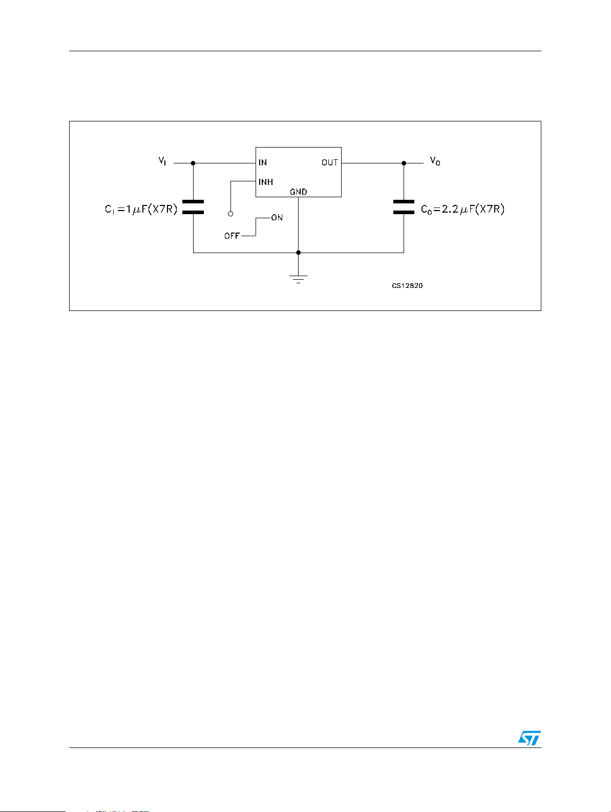
4 Typical application
Figure 3. Application circuit
Note: Inhibit pin is not internally pulled-up then it must not be left floating. Disable the device when
connected to GND or to a positive voltage less than 0.18 V.
6/23
LD2981ABxx - LD2981Cxx Electrical characteristics
5 Electrical characteristics
Table 5. Electrical characteristics for LD2981AB (TJ = 25 °C, VI = V
C
= 2.2 µF (X7R), IO = 1 mA, V
O
= 2 V, unless otherwise specified).
INH
O(NOM)
+1 V, CI = 1 µF (X7R),
Symbol Parameter Test conditions Min. Typ. Max. Unit
V
ΔV
Operating input voltage 2.5 16 V
OP
I
= 1 mA 2.481 2.5 2.518
O
V
O
V
O
V
O
V
O
V
O
V
O
V
O
V
O
V
O
V
O
V
O
O
Output voltage
Output voltage
Output voltage
Output voltage
Output voltage
Output voltage
Output voltage
Output voltage
Output voltage
Output voltage
Output voltage
Line regulation
= 1 to 100 mA 2.475 2.525
O
= 1 to 100 mA, TJ= -40 to 125°C 2.437 2.562
I
O
I
= 1 mA 2.828 2.85 2.872
O
= 1 to 100 mA 2.822 2.878
O
= 1 to 100 mA, TJ= -40 to 125°C 2.779 2.921
I
O
I
= 1 mA 2.977 3 3.023
O
= 1 to 100 mA 2.970 3.030
O
= 1 to 100 mA, TJ= -40 to 125°C 2.925 3.075
I
O
I
= 1 mA 3.176 3.2 3.224
O
= 1 to 100 mA 3.168 3.232
O
= 1 to 100 mA, TJ= -40 to 125°C 3.12 3.28
I
O
I
= 1 mA 3.275 3.3 3.325
O
= 1 to 100 mA 3.267 3.333
O
= 1 to 100 mA, TJ= -40 to 125°C 3.217 3.383
I
O
I
= 1 mA 3.573 3.6 3.627
O
= 1 to 100 mA 3.564 3.636
O
= 1 to 100 mA, TJ= -40 to 125°C 3.510 3.690
I
O
I
= 1 mA 3.771 3.8 3.829
O
= 1 to 100 mA 3.762 3.838
O
= 1 to 100 mA, TJ= -40 to 125°C 3.705 3.895
I
O
I
= 1 mA 3.97 4 4.03
O
= 1 to 100 mA 3.96 4.04
O
= 1 to 100 mA, TJ= -40 to 125°C 3.9 4.1
I
O
I
= 1 mA 4.664 4.7 4.735
O
= 1 to 100 mA 4.653 4.747
O
= 1 to 100 mA, TJ= -40 to 125°C 4.582 4.817
I
O
I
= 1 mA 4.813 4.85 4.887
O
= 1 to 100 mA 4.801 4.899
O
= 1 to 100 mA, TJ= -40 to 125°C 4.729 4.971
I
O
I
= 1 mA 4.962 5 5.038
O
= 1 to 100 mA 4.950 5.050
O
= 1 to 100 mA, TJ= -40 to 125°C 4.875 5.125
I
O
V
T
+ 1 < VIN < 16 V, IO = 1 mA 0.003 0.014
O(NOM)
= -40 to 125°C 0.032
J
%/V
VI
VI
VI
VI
VI
VI
VI
VI
VI
VI
VI
7/23
 Loading...