

ST LD2981ABM25TR, LD2981ABU25TR, LD2981CU25TR, LD2981ABM30TR, LD2981ABU30TR User Manual
...
Ultra low drop voltage regulators with inhibit
low ESR output capacitors compatible
Features
■ Stable with low ESR ceramic capacitors
■ Ultra low dropout voltage (0.17 V typ. at 100
mA load, 7 mV typ. at 1 mA load)
■ Very low quiescent current (80 µA typ. at no
load in on mode; max 1 µA in off mode)
■ Guaranteed output current up to 100mA
■ Logic-controlled electronic shutdown
■ Output voltage of 2.5; 3.0; 3.3; 5.0 V
■ Internal current and thermal limit
■ ± 0.75 % tolerance output voltage available (A
version)
■ Output low noise voltage 160 µV
■
Temperature range: -40 to 125 °C
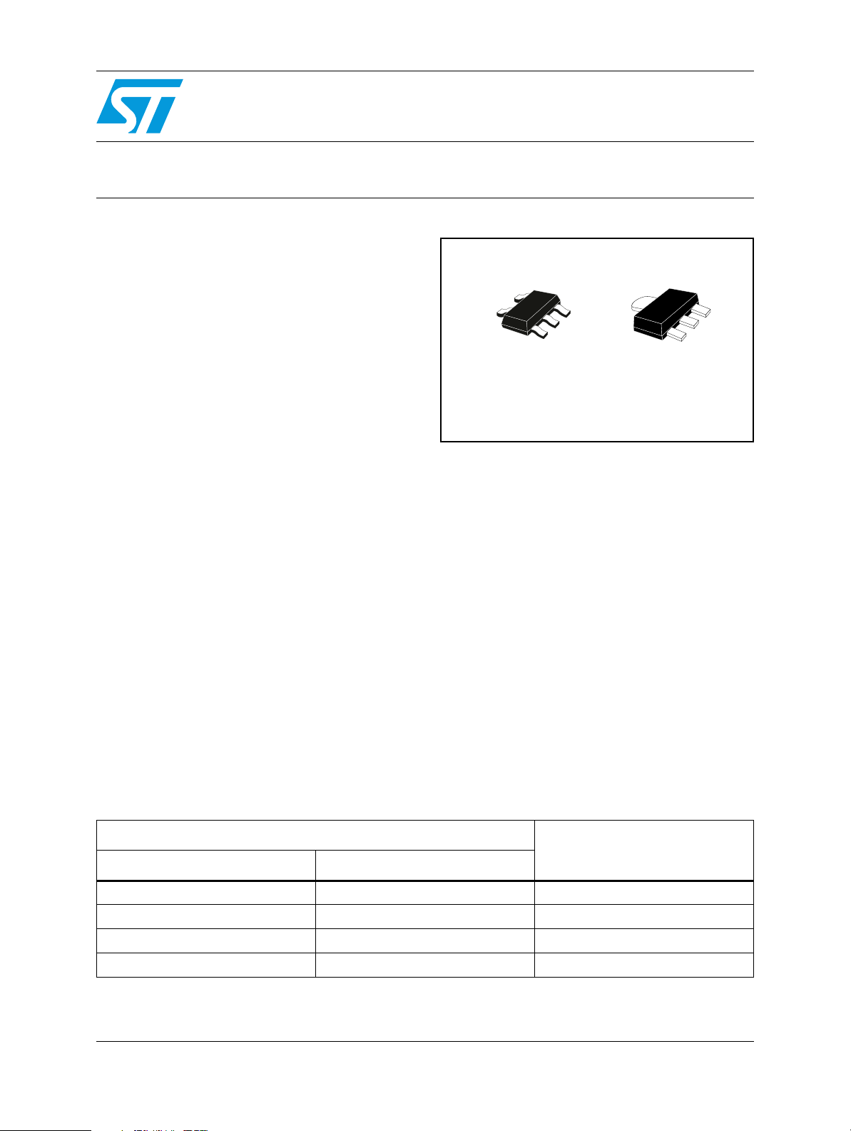
■ Smallest package SOT23-5L and SOT-89
■ Fast dynamic response to line and load
changes
RMS
LD2981ABxx
LD2981Cxx
SOT-89SOT23-5L
logic control function is available on pin n° 3 (TTL
compatible). This means that when thedevice is
used as local regulator, it is possible to put a part
of the board in standby, decreasing the total
power consumption. The LD2981AB/C is
designed to work with low ESR ceramic capacitor.
Typical applications are in cellular phone,
palmtop/laptop computer, personal digital
assistant (PDA), personal stereo, camcorder and
camera.
Description
The LD2981AB/C series are 100 mA fixed-output
voltage regulator. The low drop-voltage and the
ultra low quiescent current make them suitable for
low noise, low power applications and in battery
powered systems.
The quiescent current in sleep mode is less than
1 µA when INHIBIT pin is pulled low. Shutdown
Table 1. Device summary
Part numbers
Output voltage
AB Versio n C Vers ion
LD2981ABXX25 LD2981CXX25 2.5 V
LD2981ABXX30 LD2981CXX30 3.0 V
LD2981ABXX33 LD2981CXX33 3.3 V
LD2981ABXX50 LD2981CXX50 5.0 V
July 2008 Rev 14 1/23
www.st.com
23

LD2981ABxx - LD2981Cxx
Contents
1 Diagram . . . . . . . . . . . . . . . . . . . . . . . . . . . . . . . . . . . . . . . . . . . . . . . . . . . 3
2 Pin configuration . . . . . . . . . . . . . . . . . . . . . . . . . . . . . . . . . . . . . . . . . . . 4
3 Maximum ratings . . . . . . . . . . . . . . . . . . . . . . . . . . . . . . . . . . . . . . . . . . . . 5
4 Typical application . . . . . . . . . . . . . . . . . . . . . . . . . . . . . . . . . . . . . . . . . . 6
5 Electrical characteristics . . . . . . . . . . . . . . . . . . . . . . . . . . . . . . . . . . . . . 7
6 Typical performance characteristics . . . . . . . . . . . . . . . . . . . . . . . . . . . 11
7 Application notes . . . . . . . . . . . . . . . . . . . . . . . . . . . . . . . . . . . . . . . . . . 14
7.1 External capacitors . . . . . . . . . . . . . . . . . . . . . . . . . . . . . . . . . . . . . . . . . . 14
7.2 Input capacitor . . . . . . . . . . . . . . . . . . . . . . . . . . . . . . . . . . . . . . . . . . . . . 14
7.3 Output capacitor . . . . . . . . . . . . . . . . . . . . . . . . . . . . . . . . . . . . . . . . . . . . 14
7.4 Important . . . . . . . . . . . . . . . . . . . . . . . . . . . . . . . . . . . . . . . . . . . . . . . . . 14
7.5 Inhibit input operation . . . . . . . . . . . . . . . . . . . . . . . . . . . . . . . . . . . . . . . . 14
7.6 Reverse current . . . . . . . . . . . . . . . . . . . . . . . . . . . . . . . . . . . . . . . . . . . . 15
8 Package mechanical data . . . . . . . . . . . . . . . . . . . . . . . . . . . . . . . . . . . . 16
9 Order codes . . . . . . . . . . . . . . . . . . . . . . . . . . . . . . . . . . . . . . . . . . . . . . . 21
10 Revision history . . . . . . . . . . . . . . . . . . . . . . . . . . . . . . . . . . . . . . . . . . . 22
2/23
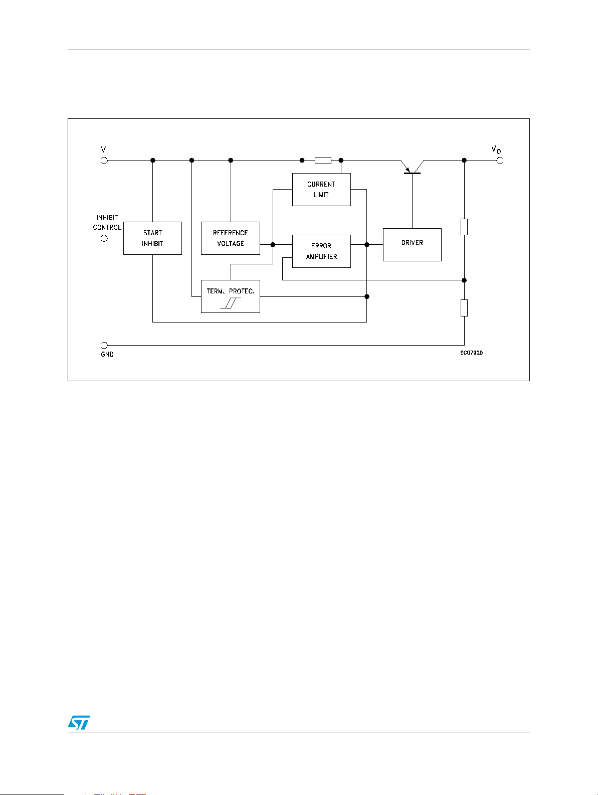
LD2981ABxx - LD2981Cxx Diagram
1 Diagram
Figure 1. Schematic diagram
3/23
Pin configuration LD2981ABxx - LD2981Cxx
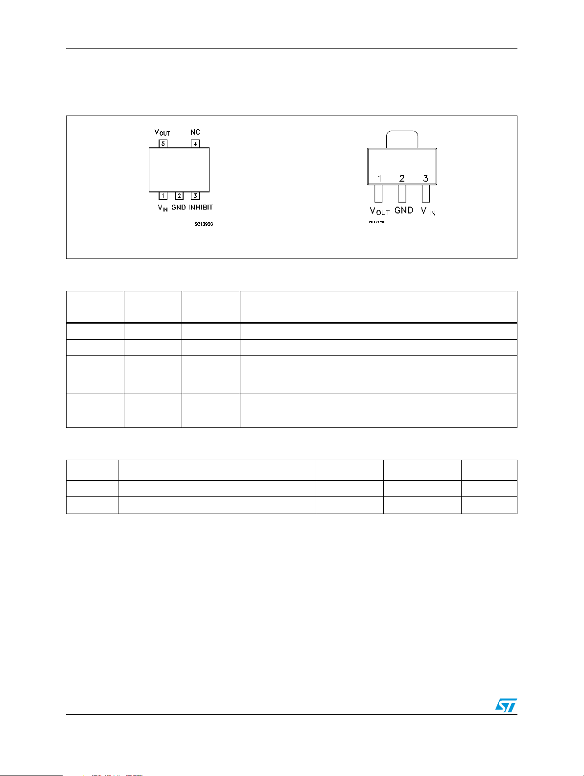
2 Pin configuration
Figure 2. Pin connections (top view)
SOT23-5L
SOT-89
Table 2. Pin description
Pin n°
SOT23-5L
13V
2 2 GND Ground pin
3INHIBIT
4 NC Not connected
51V
Pin n°
SOT-89
Symbol Name and function
IN
Input port
Control switch ON/OFF. Inhibit is not internally pulled-up; it cannot be
left floating. Disable the device when connected to GND or to a
positive voltage less than 0.18 V
OUT
Output port
Table 3. Thermal data
Symbol Parameter SOT23-5L SOT-89 Unit
R
R
thJC
thJA
Thermal resistance junction-case 81 15 °C/W
Thermal resistance junction-ambient 255 110 °C/W
4/23
LD2981ABxx - LD2981Cxx Maximum ratings
3 Maximum ratings
Table 4. Absolute maximum ratings
Symbol Parameter Value Unit
T
V
T
V
INH
I
O
P
STG
OP
I
D
DC input voltage -0.3 to 16 V
INHIBIT input voltage -0.3 to 16 V
Output current Internally limited
Power dissipation Internally limited
Storage temperature range -55 to 150 °C
Operating junction temperature range -40 to 125 °C
Note: Absolute maximum ratings are those values beyond which damage to the device may occur.
Functional operation under these condition is not implied.
5/23
Typical application LD2981ABxx - LD2981Cxx
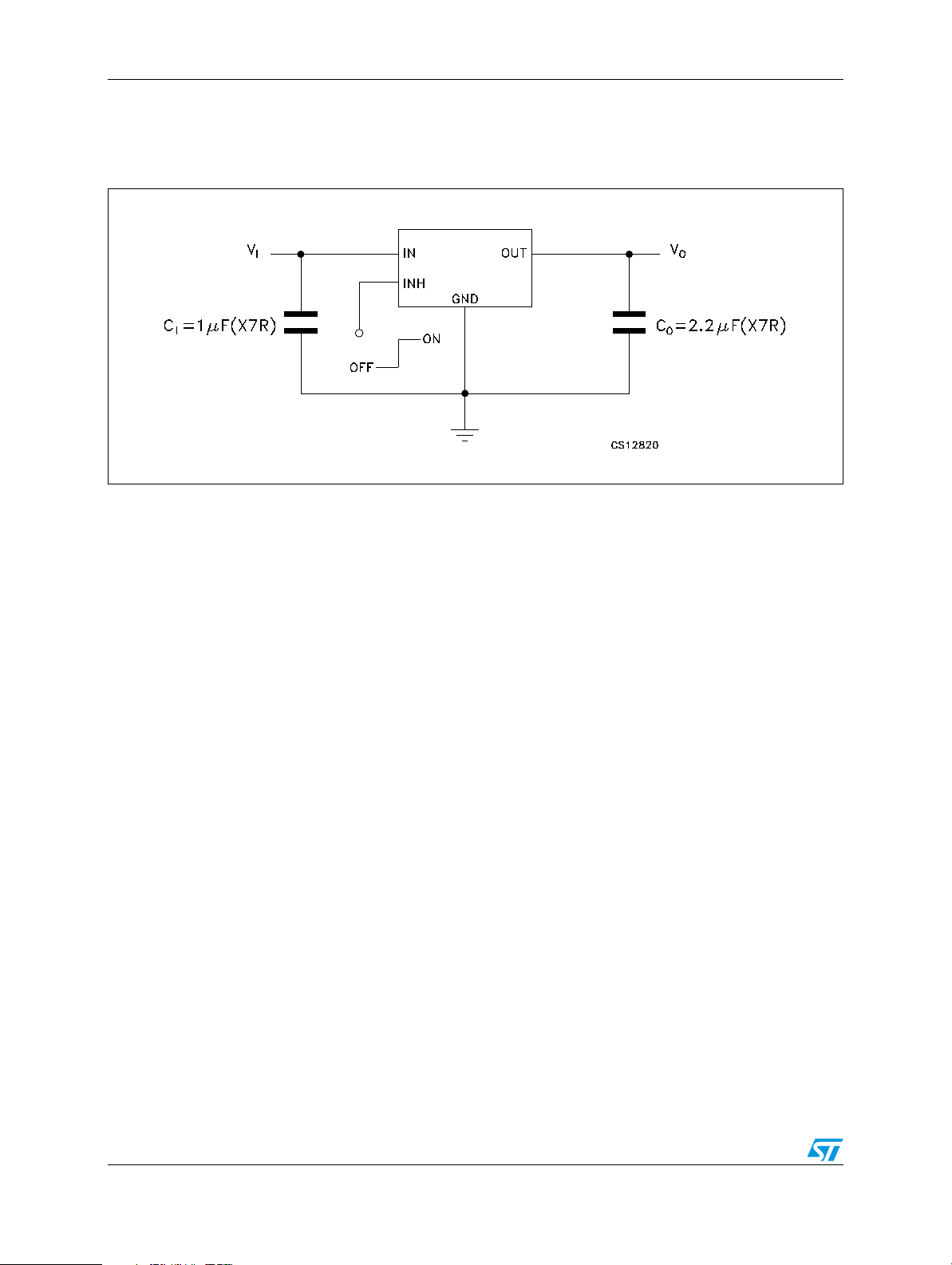
4 Typical application
Figure 3. Application circuit
Note: Inhibit pin is not internally pulled-up then it must not be left floating. Disable the device when
connected to GND or to a positive voltage less than 0.18 V.
6/23
LD2981ABxx - LD2981Cxx Electrical characteristics
5 Electrical characteristics
Table 5. Electrical characteristics for LD2981AB (TJ = 25 °C, VI = V
C
= 2.2 µF (X7R), IO = 1 mA, V
O
= 2 V, unless otherwise specified).
INH
O(NOM)
+1 V, CI = 1 µF (X7R),
Symbol Parameter Test conditions Min. Typ. Max. Unit
V
ΔV
Operating input voltage 2.5 16 V
OP
I
= 1 mA 2.481 2.5 2.518
O
V
O
V
O
V
O
V
O
V
O
V
O
V
O
V
O
V
O
V
O
V
O
O
Output voltage
Output voltage
Output voltage
Output voltage
Output voltage
Output voltage
Output voltage
Output voltage
Output voltage
Output voltage
Output voltage
Line regulation
= 1 to 100 mA 2.475 2.525
O
= 1 to 100 mA, TJ= -40 to 125°C 2.437 2.562
I
O
I
= 1 mA 2.828 2.85 2.872
O
= 1 to 100 mA 2.822 2.878
O
= 1 to 100 mA, TJ= -40 to 125°C 2.779 2.921
I
O
I
= 1 mA 2.977 3 3.023
O
= 1 to 100 mA 2.970 3.030
O
= 1 to 100 mA, TJ= -40 to 125°C 2.925 3.075
I
O
I
= 1 mA 3.176 3.2 3.224
O
= 1 to 100 mA 3.168 3.232
O
= 1 to 100 mA, TJ= -40 to 125°C 3.12 3.28
I
O
I
= 1 mA 3.275 3.3 3.325
O
= 1 to 100 mA 3.267 3.333
O
= 1 to 100 mA, TJ= -40 to 125°C 3.217 3.383
I
O
I
= 1 mA 3.573 3.6 3.627
O
= 1 to 100 mA 3.564 3.636
O
= 1 to 100 mA, TJ= -40 to 125°C 3.510 3.690
I
O
I
= 1 mA 3.771 3.8 3.829
O
= 1 to 100 mA 3.762 3.838
O
= 1 to 100 mA, TJ= -40 to 125°C 3.705 3.895
I
O
I
= 1 mA 3.97 4 4.03
O
= 1 to 100 mA 3.96 4.04
O
= 1 to 100 mA, TJ= -40 to 125°C 3.9 4.1
I
O
I
= 1 mA 4.664 4.7 4.735
O
= 1 to 100 mA 4.653 4.747
O
= 1 to 100 mA, TJ= -40 to 125°C 4.582 4.817
I
O
I
= 1 mA 4.813 4.85 4.887
O
= 1 to 100 mA 4.801 4.899
O
= 1 to 100 mA, TJ= -40 to 125°C 4.729 4.971
I
O
I
= 1 mA 4.962 5 5.038
O
= 1 to 100 mA 4.950 5.050
O
= 1 to 100 mA, TJ= -40 to 125°C 4.875 5.125
I
O
V
T
+ 1 < VIN < 16 V, IO = 1 mA 0.003 0.014
O(NOM)
= -40 to 125°C 0.032
J
%/V
VI
VI
VI
VI
VI
VI
VI
VI
VI
VI
VI
7/23

Electrical characteristics LD2981ABxx - LD2981Cxx
Table 5. Electrical characteristics for LD2981AB (continued) (TJ = 25 °C, VI = V
1 µF (X7R), C
= 2.2 µF (X7R), IO = 1 mA, V
O
= 2 V, unless otherwise specified).
INH
O(NOM)
+1 V, CI =
Symbol Parameter Test conditions Min. Typ. Max. Unit
I
= 0 80 100
O
= 0, TJ= -40 to 125°C 150
I
O
= 1 mA 100 150
I
O
= 1 mA, TJ= -40 to 125°C 200
Quiescent current
ON MODE
I
Q
OFF MODE
I
O
= 25 mA 250 400
I
O
= 25 mA, TJ= -40 to 125°C 800
I
O
= 100 mA 1000 1300
I
O
= 100 mA, TJ= -40 to 125°C 2600
I
O
< 0.3 V 0.8
V
INH
< 0.15 V, TJ= -40 to 125°C 2
V
INH
IO = 0 1 3
I
= 0, TJ= -40 to 125°C 5
O
= 1mA 7 10
I
O
= 1mA, TJ= -40 to 125°C 15
I
V
DROP
Dropout voltage
Short circuit current RL = 0 150 mA
I
SC
(1)
SVR Supply voltage rejection C
V
V
I
T
SHDN
1. For VO < 2.5 V dropout voltage can be calculated according to the minimum input voltage in full temperature range.
Inhibit input logic low LOW = Output OFF, TJ= -40 to 125°C 0.18 V
INH
Inhibit input logic high HIGH = Output ON, TJ= -40 to 125°C 1.6 V
INL
Inhibit input current
INH
Output noise voltage BW = 300 Hz to 50 KHz, CO = 10µF 160 µV
e
N
Thermal shutdown 170 °C
O
= 25mA 70 100
I
O
= 25mA, TJ= -40 to 125°C 150
I
O
= 100mA 180 250
I
O
= 100mA, TJ= -40 to 125°C 375
I
O
= 10µF, f = 1KHz 63 dB
O
= 0V, TJ= -40 to 125°C 0 -1
V
INH
V
= 5V, TJ= -40 to 125°C 5 15
INH
mV
µA
µA
RMS
8/23

LD2981ABxx - LD2981Cxx Electrical characteristics
Table 6. Electrical characteristics for LD2981C (TJ = 25 °C, VI = V
C
= 2.2 µF (X7R), IO = 1 mA, V
O
= 2 V, unless otherwise specified)
INH
O(NOM)
+1 V, CI = 1 µF (X7R),
Symbol Parameter Test conditions Min. Typ. Max. Unit
V
Operating input voltage 2.5 16 V
OP
I
= 1 mA 1.478 1.5 1.522
O
V
O
V
O
V
O
V
O
V
O
V
O
V
O
V
O
V
O
V
O
V
O
V
O
Output voltage
Output voltage
Output voltage
Output voltage
Output voltage
Output voltage
Output voltage
Output voltage
Output voltage
Output voltage
Output voltage
Output voltage
= 1 to 100 mA 1.470 1.530
O
= 1 to 100 mA, TJ= -40 to 125°C 1.445 1.555
I
O
I
= 1 mA 1.777 1.8 1.822
O
= 1 to 100 mA 1.764 1.836
O
= 1 to 100 mA, TJ= -40 to 125°C 1.737 1.863
I
O
I
= 1 mA 2.468 2.5 2.531
O
= 1 to 100 mA 2.45 2.55
O
= 1 to 100 mA, TJ= -40 to 125°C 2.412 2.587
I
O
I
= 1 mA 2.814 2.85 2.885
O
= 1 to 100 mA 2.793 2.907
O
= 1 to 100 mA, TJ= -40 to 125°C 2.75 2.949
I
O
I
= 1 mA 2.962 3 3.037
O
= 1 to 100 mA 2.94 3.06
O
= 1 to 100 mA, TJ= -40 to 125°C 2.895 3.105
I
O
I
= 1 mA 3.16 3.2 3.24
O
= 1 to 100 mA 3.136 3.264
O
= 1 to 100 mA, TJ= -40 to 125°C 3.088 3.312
I
O
I
= 1 mA 3.258 3.3 3.341
O
= 1 to 100 mA 3.234 3.366
O
= 1 to 100 mA, TJ= -40 to 125°C 3.184 3.415
I
O
I
= 1 mA 3.555 3.6 3.645
O
= 1 to 100 mA 3.528 3.672
O
= 1 to 100 mA, TJ= -40 to 125°C 3.474 3.726
I
O
I
= 1 mA 3.752 3.8 3.847
O
= 1 to 100 mA 3.724 3.876
O
= 1 to 100 mA, TJ= -40 to 125°C 3.667 3.933
I
O
I
= 1 mA 3.95 4 4.05
O
= 1 to 100 mA 3.92 4.08
O
= 1 to 100 mA, TJ= -40 to 125°C 3.86 4.14
I
O
I
= 1 mA 4.641 4.7 4.758
O
= 1 to 100 mA 4.606 4.794
O
= 1 to 100 mA, TJ= -40 to 125°C 4.535 4.864
I
O
I
= 1 mA 4.789 4.85 4.91
O
= 1 to 100 mA 4.753 4.947
O
= 1 to 100 mA, TJ= -40 to 125°C 4.68 5.019
I
O
VI
VI
VI
VI
VI
VI
VI
VI
VI
VI
VI
VI
9/23

Electrical characteristics LD2981ABxx - LD2981Cxx
Table 6. Electrical characteristics for LD2981C (continued) (TJ = 25 °C, VI = V
µF (X7R), C
= 2.2 µF (X7R), IO = 1 mA, V
O
= 2 V, unless otherwise specified)
INH
O(NOM)
+1 V, CI = 1
Symbol Parameter Test conditions Min. Typ. Max. Unit
I
= 1 mA 4.937 5 5.062
O
V
ΔV
Output voltage
O
Line regulation
O
Quiescent current
ON MODE
I
Q
OFF MODE
= 1 to 100 mA 4.9 5.1
O
= 1 to 100 mA, TJ= -40 to 125°C 4.825 5.175
I
O
V
T
I
I
I
I
I
I
I
I
V
V
O
O
O
O
O
O
O
O
+ 1 < VIN < 16 V, IO = 1 mA 0.003 0.014
O(NOM)
= -40 to 125°C 0.032
J
= 0 80 100
= 0, TJ= -40 to 125°C 150
= 1 mA 100 150
= 1 mA, TJ= -40 to 125°C 200
= 25 mA 250 400
= 25 mA, TJ= -40 to 125°C 800
= 100 mA 1000 1300
= 100 mA, TJ= -40 to 125°C 2600
< 0.3 V 0.8
INH
< 0.15 V, TJ= -40 to 125°C 2
INH
%/V
IO = 0 1 3
I
= 0, TJ= -40 to 125°C 5
O
= 1 mA 7 10
I
O
= 1 mA, TJ= -40 to 125°C 15
I
V
DROP
Dropout voltage
Short circuit current RL = 0 150 mA
I
SC
(1)
SVR Supply voltage rejection C
V
V
I
T
SHDN
1. For VO < 2.5 V dropout voltage can be calculated according to the minimum input voltage in full temperature range.
Inhibit input logic low LOW = Output OFF, TJ= -40 to 125°C 0.18 V
INH
Inhibit input logic high HIGH = Output ON, TJ= -40 to 125°C 1.6 V
INL
Inhibit input current
INH
Output noise voltage BW = 300 Hz to 50 KHz, CO = 10µF 160 µV
e
N
Thermal shutdown 170 °C
O
= 25 mA 70 100
I
O
= 25 mA, TJ= -40 to 125°C 150
I
O
= 100 mA 180 250
I
O
= 100 mA, TJ= -40 to 125°C 375
I
O
= 10µF, f = 1KHz 63 dB
O
V
= 0V, TJ= -40 to 125°C 0 -1
INH
V
= 5V, TJ= -40 to 125°C 5 15
INH
mV
VI
µA
µF
RMS
10/23

LD2981ABxx - LD2981Cxx Typical performance characteristics
6 Typical performance characteristics
(TJ = 25 °C, VI = V
O(NOM)
+1 V, CI = 1 µF (X7R), CO = 2.2 µF (X7R), V
= 2 V, unless
INH
otherwise specified).
Figure 4. Output voltage vs temperature Figure 5. Dropout voltage vs temperature
Figure 6. Line regulation vs temperature Figure 7. Load regulation vs temperature
Figure 8. Dropout voltage vs temperature Figure 9. Quiescent current vs temperature
11/23

Typical performance characteristics LD2981ABxx - LD2981Cxx
Figure 10. Quiescent current vs output
Figure 12. Quiescent current vs input voltage Figure 13. Dropout voltage vs output current
current
Figure 11. Off mode quiescent current vs
temperature
Figure 14. Inhibit input current vs temperature Figure 15. Inhibit voltage vs temperature
12/23

LD2981ABxx - LD2981Cxx Typical performance characteristics
Figure 16. Supply voltage rejection vs
Figure 18. Best case: highest output version Figure 19. Worst case: lowest output version
frequency
Figure 17. Noise voltage vs frequency
Figure 20. Load transient response Figure 21. Line transient response
VO = 4.7V, IO = 1 to 100mA, CO = 4.7µF (X7R)
VI = [V
(X7R)
+1V], VO = 4.7V, IO = 100mA, CO = 4.7µF
O(NOM)
13/23

Application notes LD2981ABxx - LD2981Cxx
7 Application notes
7.1 External capacitors
Like any low-dropout regulator, the LD2981 requires external capacitors for regulator
stability. This capacitor must be selected to meet the requirements of minimum capacitance
and equivalent series resistance. We suggest to solder input and output capacitors as close
as possible to the relative pins.
7.2 Input capacitor
An input capacitor whose value is 1 µF is required with the LD2981 (amount of capacitance
can be increased without limit). This capacitor must be located a distance of not more than
0.5" from the input pin of the device and returned to a clean analog ground. Any good quality
ceramic, tantalum or film capacitors can be used for this capacitor.
7.3 Output capacitor
The LD2981 is designed specifically to work with ceramic output capacitors. It may also be
possible to use Tantalum capacitors, but these are not as attractive for reasons of size and
cost. By the way, the output capacitor must meet both the requirement for minimum amount
of capacitance and ESR (equivalent series resistance) value. The Figure 3 and Figure 4
show the allowable ESR range as a function of the output capacitance. These curves
represent the stability region over the full temperature and I
gain, the stability improves for higher output versions and so the suggested minimum output
capacitor value, if low ESR ceramic type is used, is 1 µF for output voltages equal or major
than 3.8 V, 2.2 µF for output voltages from 2.85 to 3.3 V, and 3.3 µF for the other versions.
However, if an output capacitor lower than the suggested one is used, it’s possible to make
stable the regulator adding a resistor in series to the capacitor (see Figure 1 and Figure 2 to
choose the right value according to the used version and keeping in account that the ESR of
ceramic capacitors has been measured @ 100 kHz).
range. Due to the different loop
O
7.4 Important
The output capacitor must maintain its ESR in the stable region over the full operating
temperature to assure stability. Also, capacitor tolerance and variation with temperature
must be considered to assure the minimum amount of capacitance is provided at all times.
This capacitor should be located not more than 0.5" from the output pin of the device and
returned to a clean analog ground.
7.5 Inhibit input operation
The inhibit pin can be used to turn OFF the regulator when pulled low, so drastically
reducing the current consumption down to less than 1 µA. When the inhibit feature is not
14/23
used, this pin must be tied to V
proper operation, the signal source used to drive the inhibit pin must be able to swing above
and below the specified thresholds listed in the electrical characteristics section under V
V
. Any slew rate can be used to drive the inhibit.
IL
to keep the regulator output ON at all times. To assure
I
IH

LD2981ABxx - LD2981Cxx Application notes
7.6 Reverse current
The power transistor used in the LD2981 has not an inherent diode connected between the
regulator input and output. If the output is forced above the input, no current will flow from
the output to the input across the series pass transistor. When a V
the output, the reverse current measured, according to the test circuit in Figure 22, flows to
the GND across the two feedback resistors. This current typical value is 160 µA. R
resistors are implanted type; typical values are, respectively, 42.6 kΩ and 51.150 kΩ.
Figure 22. Reverse current test circuit
voltage is applied on
REV
1
and R2
15/23

Package mechanical data LD2981ABxx - LD2981Cxx
8 Package mechanical data
In order to meet environmental requirements, ST offers these devices in ECOPACK®
packages. These packages have a lead-free second level interconnect. The category of
second Level Interconnect is marked on the package and on the inner box label, in
compliance with JEDEC Standard JESD97. The maximum ratings related to soldering
conditions are also marked on the inner box label. ECOPACK is an ST trademark.
ECOPACK specifications are available at: www.st.com.
16/23

LD2981ABxx - LD2981Cxx Package mechanical data
SOT-89 mechanical data
mm. mils.
Dim.
Min. Typ. Max. Min. Typ. Max.
A 1.4 1.6 55.1 63.0
B 0.44 0.56 17.3 22.0
B1 0.36 0.48 14.2 18.9
C0.35 0.44 13.8 17.3
C1 0.35 0.44 13.8 17.3
D 4.4 4.6 173.2 181.1
D1 1.62 1.83 63.8 72.0
E2.29 2.6 90.2 102.4
e 1.42 1.57 55.9 61.8
e1 2.92 3.07 115.0 120.9
H 3.94 4.25 155.1 167.3
L0.89 1.2 35.0 47.2
P025H
17/23

Package mechanical data LD2981ABxx - LD2981Cxx
SOT23-5L mechanical data
mm. mils.
Dim.
Min. Typ. Max. Min. Typ. Max.
A0.90 1.45 35.4 57.1
A1 0.00 0.10 0.0 3.9
A2 0.901.30 35.4 51.2
b 0.35 0.50 13.7 19.7
C0.09 0.20 3.5 7.8
D2.80 3.00 110.2 118.1
E 1.50 1.75 59.0 68.8
e0.95 37.4
H 2.60 3.00 102.3 118.1
L 0.10 0.60 3.9 23.6
18/23
7049676D

LD2981ABxx - LD2981Cxx Package mechanical data
Tape & reel SOT23-xL mechanical data
Dim.
Min. Typ. Max. Min. Typ. Max.
A180 7.086
C 12.8 13.0 13.2 0.504 0.512 0.519
D 20.2 0.795
N60 2.362
T 14.4 0.567
Ao 3.133.233.33 0.123 0.127 0.131
Bo 3.07 3.17 3.27 0.120 0.124 0.128
Ko 1.27 1.37 1.47 0.050 0.054 0.0.58
Po 3.9 4.0 4.1 0.153 0.157 0.161
P 3.9 4.0 4.1 0.153 0.157 0.161
mm. inch.
19/23

Package mechanical data LD2981ABxx - LD2981Cxx
Tape & reel SOT-89 mechanical data
Dim.
Min. Typ. Max. Min. Typ. Max.
A180 7.086
C 12.8 13.0 13.2 0.504 0.512 0.519
D 20.2 0.795
N60 2.362
T 14.4 0.567
Ao 4.70 4.804.90 0.185 0.189 0.193
Bo 4.30 4.40 4.50 0.169 0.173 0.177
Ko 1.70 1.801.90 0.067 0.071 0.075
Po 3.9 4.0 4.1 0.153 0.157 0.161
P7.98.0 8.1 0.311 0.315 0.319
mm. inch.
20/23

LD2981ABxx - LD2981Cxx Order codes
9 Order codes
Table 7. Order codes
AB Version C Version
Output voltage
SOT23-5L SOT-89 SOT23-5L SOT-89
LD2981ABM25TR LD2981ABU25TR
LD2981ABM30TR LD2981ABU30TR
LD2981ABM33TR LD2981ABU33TR LD2981CM33TR LD2981CU33TR 3.3 V
LD2981ABM50TR LD2981ABU50TR LD2981CM50TR LD2981CU50TR 5.0 V
1. Available on request.
(1)
(1)
LD2981CM30TR LD2981CU30TR
LD2981CU25TR
(1)
(1)
2.5 V
3.0 V
21/23

Revision history LD2981ABxx - LD2981Cxx
10 Revision history
Table 8. Document revision history
Date Revision Changes
25-Jul-2006 12 Order codes updated.
14-Feb-2008 13 Added: Table 1 on page 1.
14-Jul-2008 14 Modified: Table 1 on page 1 and Table 7 on page 21.
22/23

LD2981ABxx - LD2981Cxx
Please Read Carefully:
Information in this document is provided solely in connection with ST products. STMicroelectronics NV and its subsidiaries (“ST”) reserve the
right to make changes, corrections, modifications or improvements, to this document, and the products and services described herein at any
time, without notice.
All ST products are sold pursuant to ST’s terms and conditions of sale.
Purchasers are solely responsible for the choice, selection and use of the ST products and services described herein, and ST assumes no
liability whatsoever relating to the choice, selection or use of the ST products and services described herein.
No license, express or implied, by estoppel or otherwise, to any intellectual property rights is granted under this document. If any part of this
document refers to any third party products or services it shall not be deemed a license grant by ST for the use of such third party products
or services, or any intellectual property contained therein or considered as a warranty covering the use in any manner whatsoever of such
third party products or services or any intellectual property contained therein.
UNLESS OTHERWISE SET FORTH IN ST’S TERMS AND CONDITIONS OF SALE ST DISCLAIMS ANY EXPRESS OR IMPLIED
WARRANTY WITH RESPECT TO THE USE AND/OR SALE OF ST PRODUCTS INCLUDING WITHOUT LIMITATION IMPLIED
WARRANTIES OF MERCHANTABILITY, FITNESS FOR A PARTICULAR PURPOSE (AND THEIR EQUIVALENTS UNDER THE LAWS
OF ANY JURISDICTION), OR INFRINGEMENT OF ANY PATENT, COPYRIGHT OR OTHER INTELLECTUAL PROPERTY RIGHT.
UNLESS EXPRESSLY APPROVED IN WRITING BY AN AUTHORIZED ST REPRESENTATIVE, ST PRODUCTS ARE NOT
RECOMMENDED, AUTHORIZED OR WARRANTED FOR USE IN MILITARY, AIR CRAFT, SPACE, LIFE SAVING, OR LIFE SUSTAINING
APPLICATIONS, NOR IN PRODUCTS OR SYSTEMS WHERE FAILURE OR MALFUNCTION MAY RESULT IN PERSONAL INJURY,
DEATH, OR SEVERE PROPERTY OR ENVIRONMENTAL DAMAGE. ST PRODUCTS WHICH ARE NOT SPECIFIED AS "AUTOMOTIVE
GRADE" MAY ONLY BE USED IN AUTOMOTIVE APPLICATIONS AT USER’S OWN RISK.
Resale of ST products with provisions different from the statements and/or technical features set forth in this document shall immediately void
any warranty granted by ST for the ST product or service described herein and shall not create or extend in any manner whatsoever, any
liability of ST.
ST and the ST logo are trademarks or registered trademarks of ST in various countries.
Information in this document supersedes and replaces all information previously supplied.
The ST logo is a registered trademark of STMicroelectronics. All other names are the property of their respective owners.
© 2008 STMicroelectronics - All rights reserved
STMicroelectronics group of companies
Australia - Belgium - Brazil - Canada - China - Czech Republic - Finland - France - Germany - Hong Kong - India - Israel - Italy - Japan -
Malaysia - Malta - Morocco - Singapore - Spain - Sweden - Switzerland - United Kingdom - United States of America
www.st.com
23/23
 Loading...