

ST LD29300P2T15R, LD29300D2T18R, LD29300D2M18R, LD29300P2T18R, LD29300P2M18R User Manual
...
3 A, very low drop voltage regulators
Features
■ Very low dropout voltage (Typ. 0.4 at 3 A)
■ Guaranteed output current up to 3 A
■ Fixed voltage with ± 1 % tolerance at 25 °C
■ Internal current and thermal limit
■ Logic controlled electronic shutdown available
in PPAK
Description
The LD29300xx is a high current, high accuracy,
low-dropout voltage regulator series. These
regulators feature 400 mV dropout voltage and
very low ground current. Designed for high
current loads, these devices are also used in
lower current, extremely low dropout-critical
systems, where their tiny dropout voltage and
ground current values are important attributes.
Typical applications are in power supply switching
post regulation, Series power supply for monitors,
Series power supply for VCRs and TVs,
Computer systems and Battery powered systems.
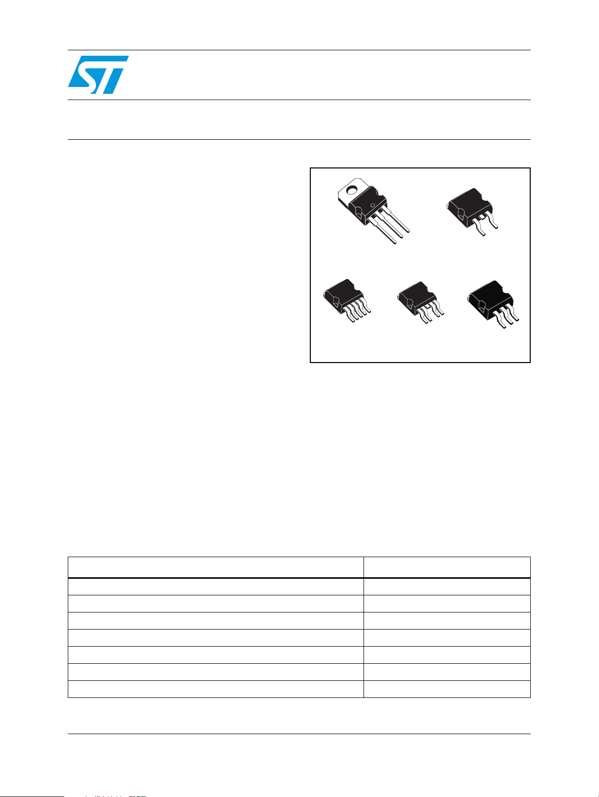
TO-220
2
P
PAK /A P2PAK
LD29300xx
D2PAK
D2PAK/A
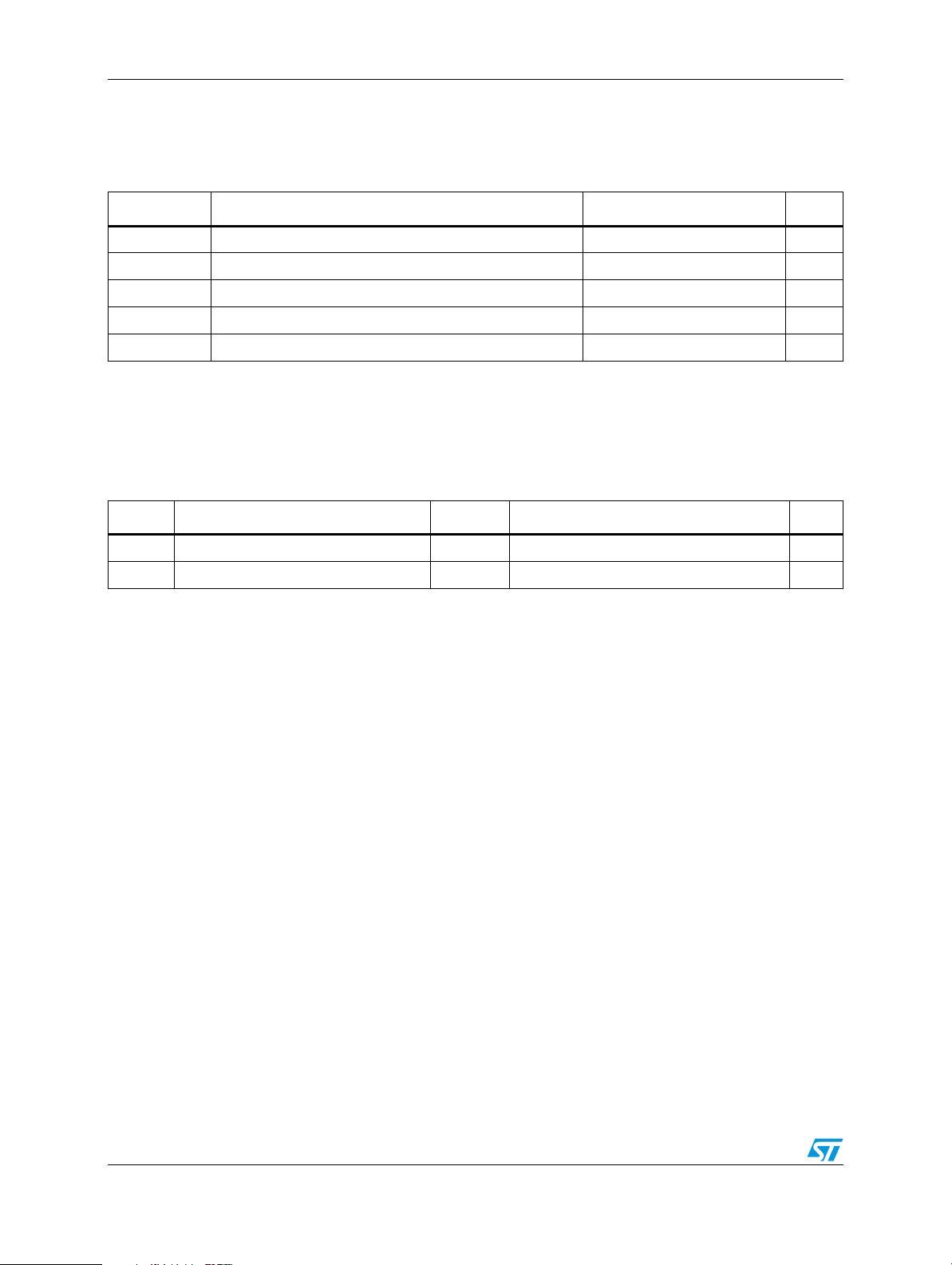
Table 1. Device summary
Part numbers Output voltages
LD29300XX15 1.5 V
LD29300XX18 1.8 V
LD29300XX25 2.5 V
LD29300XX33 3.3 V
LD29300XX50 5.0 V
LD29300XX80 8.0 V
LD29300XX ADJ
July 2008 Rev 12 1/26
www.st.com
26

Contents LD29300xx
Contents
1 Diagram . . . . . . . . . . . . . . . . . . . . . . . . . . . . . . . . . . . . . . . . . . . . . . . . . . . 3
2 Pin configuration . . . . . . . . . . . . . . . . . . . . . . . . . . . . . . . . . . . . . . . . . . . 4
3 Typical application . . . . . . . . . . . . . . . . . . . . . . . . . . . . . . . . . . . . . . . . . . 5
4 Maximum ratings . . . . . . . . . . . . . . . . . . . . . . . . . . . . . . . . . . . . . . . . . . . . 6
5 Electrical characteristics . . . . . . . . . . . . . . . . . . . . . . . . . . . . . . . . . . . . . 7
6 Typical characteristics . . . . . . . . . . . . . . . . . . . . . . . . . . . . . . . . . . . . . . 14
7 Package mechanical data . . . . . . . . . . . . . . . . . . . . . . . . . . . . . . . . . . . . 17
8 Order codes . . . . . . . . . . . . . . . . . . . . . . . . . . . . . . . . . . . . . . . . . . . . . . . 24
9 Revision history . . . . . . . . . . . . . . . . . . . . . . . . . . . . . . . . . . . . . . . . . . . 25
2/26
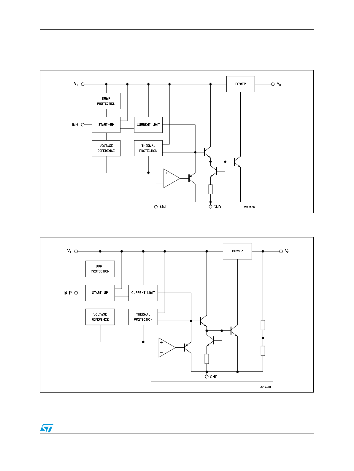
LD29300xx Diagram
1 Diagram
Figure 1. Schematic diagram for adjustable version
Figure 2. Schematic diagram for fixed version
* Only for version with inhibit function.
3/26
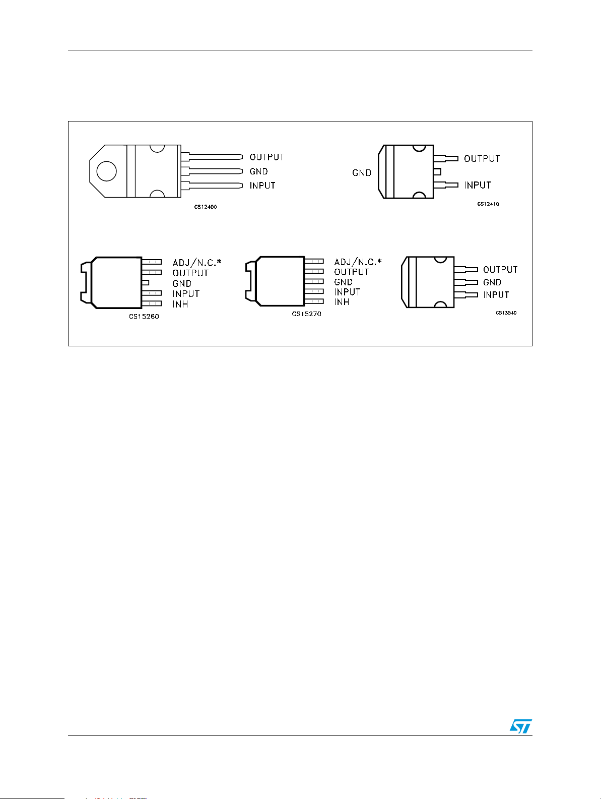
Pin configuration LD29300xx
2 Pin configuration
Figure 3. Pin connections (top view)
TO-220
P2PAK
* Not connected for fixed version.
P2PAK/A
D2PAK
2
D
PAK/A
4/26
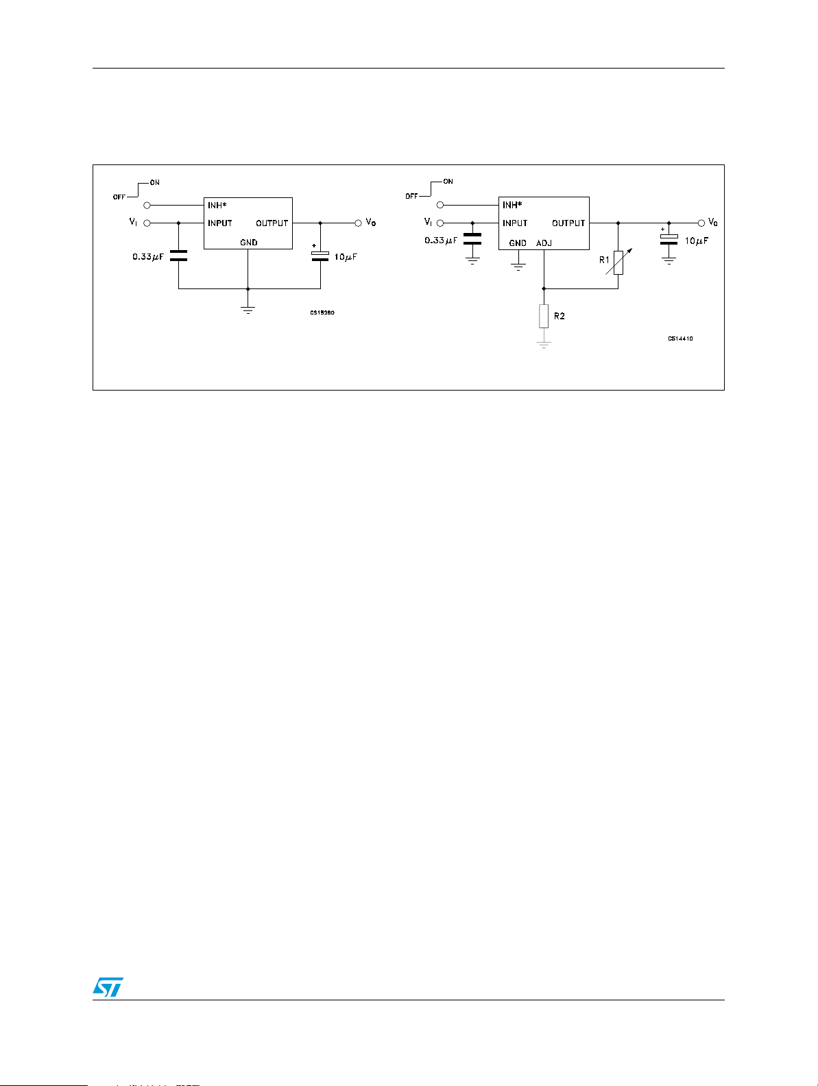
LD29300xx Typical application
3 Typical application
Figure 4. Application circuit
* Only for version with inhibit function.
VO = V
(1 + R1/R2)
REF
5/26
Maximum ratings LD29300xx
4 Maximum ratings
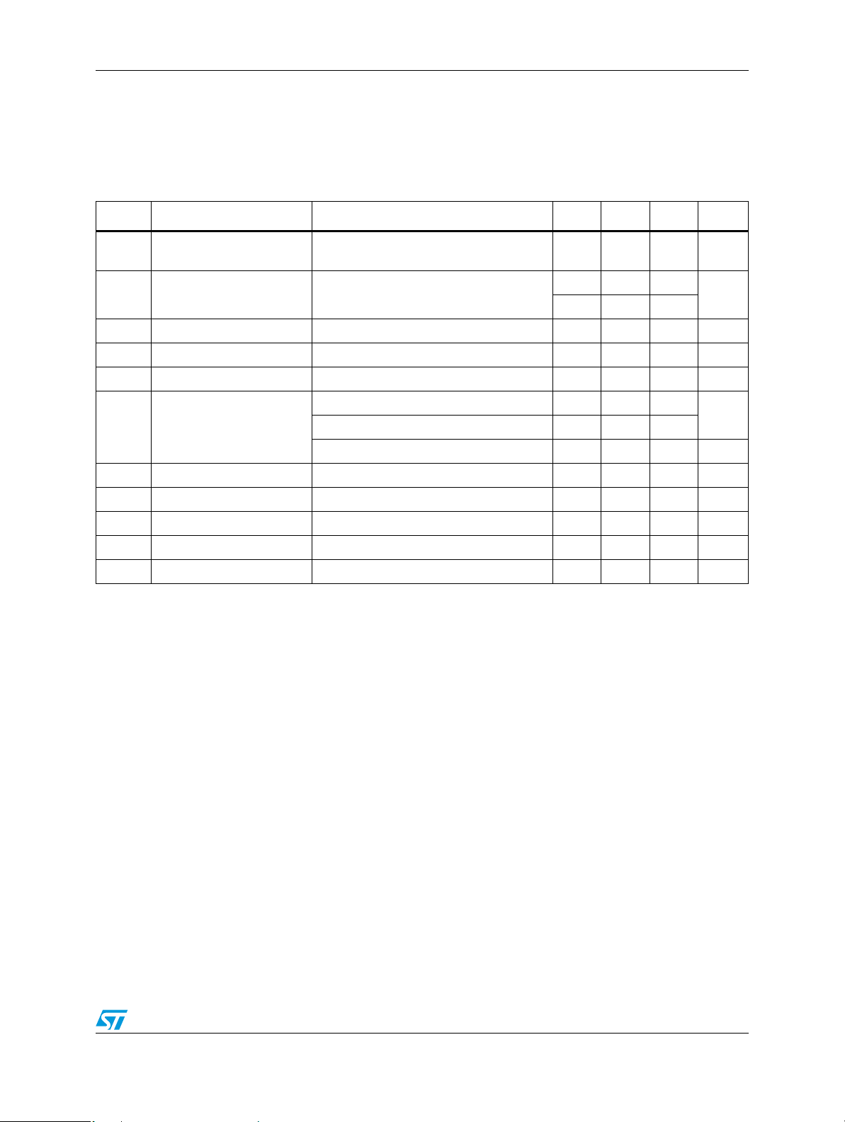
Table 2. Absolute maximum ratings
Symbol Parameter Value Unit
V
I
I
O
P
D
T
STG
T
OP
1. Above 14 V the device is automatically in shut-down.
DC input voltage 30
Output current Internally limited mA
Power dissipation Internally limited mW
Storage temperature range -55 to 150 °C
Operating junction temperature range -40 to 125 °C
Note: Absolute maximum ratings are those values beyond which damage to the device may occur.
Functional operation under these conditions is not implied.
Table 3. Thermal data
Symbol Parameter TO-220 D2PA K- P2PAK-D2PAK/A-P2PA K/ A Un it
(1)
V
R
R
Thermal resistance junction-ambient 50 60 °C/W
thJA
Thermal resistance junction-case 3 3 °C/W
thJC
6/26
LD29300xx Electrical characteristics
5 Electrical characteristics
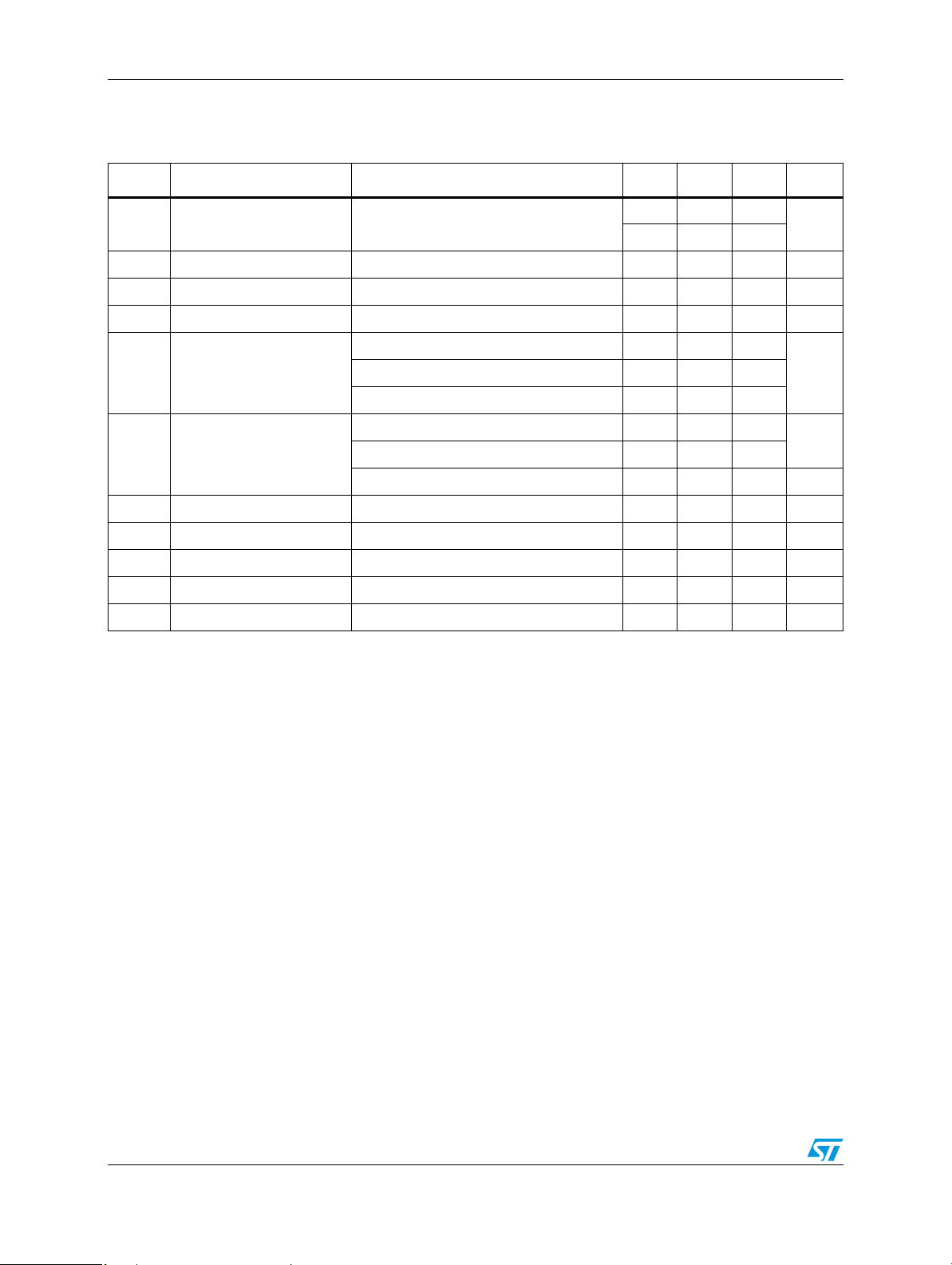
Table 4. Electrical characteristics of LD29300#15
(I
= 10 mA, TJ = 25 °C, VI = 3.5 V, V
O
INH
= 2 V
(1)
, CI = 330 nF, CO = 10 µF, unless otherwise
specified)
Symbol Parameter Test conditions Min. Typ. Max. Unit
Minimum operating input
V
I
voltage
Output voltage
V
O
ΔV
ΔV
Load regulation IO = 10mA to 3A 0.2 1.0 %
O
Line regulation VI = 3 to 13V 0.06 0.5 %
O
SVR Supply voltage rejection f = 120 Hz, V
I
Quiescent current
q
Short circuit current VI - VO = 5.5V 4.5 A
I
sc
Control input logic low OFF MODE
V
IL
V
Control input logic high ON MODE
IH
I
Control input current TJ = -40 to 125°C, V
INH
eN Output noise voltage B
1. Only for version with Inhibit function.
2. Guaranteed by design
= 10mA to 3A, TJ = -40 to 125°C 2.5 V
I
O
= 10mA to 3A, VI = 3 to 7V
I
O
= -40 to 125°C
T
J
= 3.5 ± 1V, IO = 1.5A
I
I
= 1.5A, TJ = -40 to 125°C 20 50
O
= 3A, TJ = -40 to 125°C 45 100
I
O
V
= 13V, V
I
= 10Hz to 100kHz, IO = 100mA 60 µV
P
= GND, TJ = -40 to 125°C 130 180 µA
INH
(1)
, TJ = -40 to 125°C 0.8 V
(1)
, TJ = -40 to 125°C 2 V
= 13V 5 10 µA
INH
1.485 1.5 1.515
1.47 1.53
(2)
65 75 dB
mA
V
RMS
7/26
Electrical characteristics LD29300xx
Table 5. Electrical characteristics of LD29300#18
(I
= 10 mA, TJ = 25 °C, VI = 3.8 V, V
O
INH
= 2 V
(1)
, CI = 330 nF, CO = 10 µF, unless otherwise
specified)
Symbol Parameter Test conditions Min. Typ. Max. Unit
= 10mA to 3A, VI = 3 to 7.3V
I
V
Output voltage
O
ΔV
ΔV
Load regulation IO = 10mA to 3A 0.2 1.0 %
O
Line regulation VI = 3 to 13V 0.06 0.5 %
O
SVR Supply voltage rejection f = 120 Hz, V
V
I
Dropout voltage
DROP
I
Quiescent current
q
I
Short circuit current VI - VO = 5.5V 4.5 A
sc
Control input logic low OFF MODE
V
IL
Control input logic high ON MODE
V
IH
Control input current TJ = -40 to 125°C, V
INH
eN Output noise voltage B
1. Only for version with Inhibit function.
2. Guaranteed by design.
3. Dropout voltage is defined as the input-to-output differential when the output voltage drops to 99 % of its nominal value with
+ 1 V applied to VI.
V
O
O
= -40 to 125°C
T
J
= 3.8 ±1V, IO = 1.5A
I
I
= 500mA, TJ = -40 to 125°C
O
= 1.5A, TJ = -40 to 125°C
O
= 3A, TJ = -40 to 125°C
I
O
I
= 1.5A, TJ = -40 to 125°C 20 50
O
= 3A, TJ = -40 to 125°C 45 100
I
O
= 13V, V
V
I
= 10Hz to 100kHz, IO = 100mA 60 µV
P
= GND, TJ = -40 to 125°C 130 180 µA
INH
(1)
, TJ = -40 to 125°C 0.8 V
(1)
, TJ = -40 to 125°C 2 V
= 13V 5 10 µA
INH
(3)
(3)
(3)
1.782 1.8 1.818
1.764 1.836
(2)
62 72 dB
0.1
0.2
0.4 0.7
mA
V
VI
RMS
8/26
 Loading...