


Features
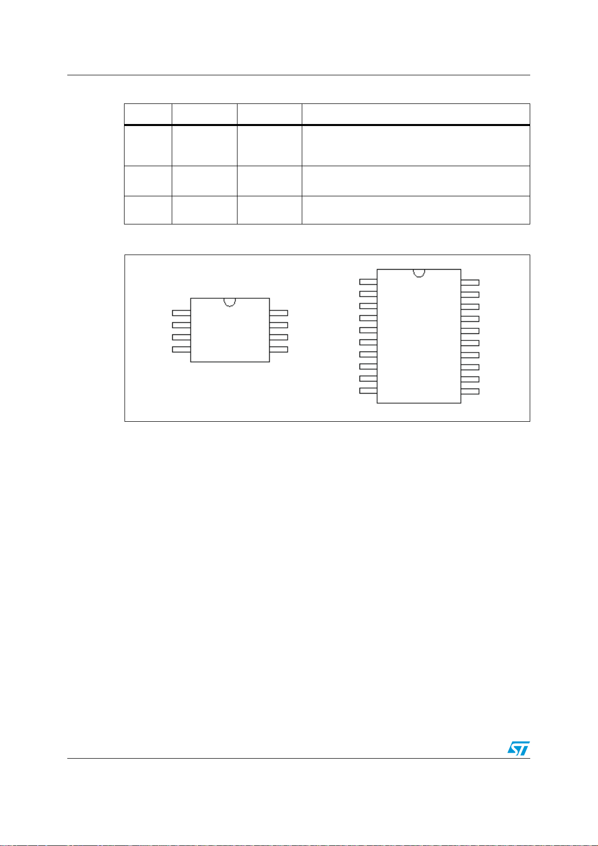
SO-8
SO-20
■ Operating DC supply voltage range 5.6 V to
31 V
■ Very low quiescent current with watchdog
disabled
■ Precision output voltage (3%)
■ Low drop voltage (180 mV typ at I
■ Reset circuit sensing the output voltage down
to 1 V
■ Programmable reset delay with external
capacitor
■ Watchdog disable input
■ Programmable watchdog timer with external
capacitor
■ Thermal shutdown and short circuit protection
■ Wide temperature range (T
= -40°C to 150°C)
j
= 150 mA)
o
L4989D
L4989MD
Low power voltage regulator
Datasheet − production data
Description
The L4989M and L4989MD are monolithic
integrated 5 V voltage regulators with a low drop
voltage at currents up to 150 mA.
The output voltage regulating element consists in
a p-channel MOS and the regulation is performed
regardless of input voltage transients up to 40 V.
The high precision of the output voltage is
obtained with a pre-trimmed reference voltage.
Table 1. Device summary
Package
SO-8 L4989D L4989D013TR
SO-20 L4989MD L4989MD013TR
The devices are protected against short circuit
and an overtemperature protection switches off
the devices in case of extremely high power
dissipation.
The L4989M and L4989MD watchdogs are active
when the Enable pin is high. Features like reset
and watchdog make this devices particularly
suitable to supply microprocessor systems in
automotive applications.
Order codes
Tube Tape and reel
April 2012 Doc ID 022376 Rev. 1 1/19
This is information on a product in full production.
www.st.com
1

Contents L4989D, L4989MD
Contents
1 Block diagram and pin configuration . . . . . . . . . . . . . . . . . . . . . . . . . . 5
2 Electrical specifications . . . . . . . . . . . . . . . . . . . . . . . . . . . . . . . . . . . . . . 7
2.1 Absolute maximum ratings . . . . . . . . . . . . . . . . . . . . . . . . . . . . . . . . . . . . . 7
2.2 Thermal data . . . . . . . . . . . . . . . . . . . . . . . . . . . . . . . . . . . . . . . . . . . . . . . 7
2.3 Electrical characteristics . . . . . . . . . . . . . . . . . . . . . . . . . . . . . . . . . . . . . . . 8
3 Application information . . . . . . . . . . . . . . . . . . . . . . . . . . . . . . . . . . . . . 11
3.1 Voltage regulator . . . . . . . . . . . . . . . . . . . . . . . . . . . . . . . . . . . . . . . . . . . 11
3.2 Reset . . . . . . . . . . . . . . . . . . . . . . . . . . . . . . . . . . . . . . . . . . . . . . . . . . . . 11
3.3 Watchdog . . . . . . . . . . . . . . . . . . . . . . . . . . . . . . . . . . . . . . . . . . . . . . . . . 12
4 Package and packing information . . . . . . . . . . . . . . . . . . . . . . . . . . . . . 13
4.1 ECOPACK® packages . . . . . . . . . . . . . . . . . . . . . . . . . . . . . . . . . . . . . . . 13
4.2 SO-8 package information . . . . . . . . . . . . . . . . . . . . . . . . . . . . . . . . . . . . 13
4.3 SO-20 package information . . . . . . . . . . . . . . . . . . . . . . . . . . . . . . . . . . . 15
4.4 SO-8 packing information . . . . . . . . . . . . . . . . . . . . . . . . . . . . . . . . . . . . . 16
4.5 SO-20 packing information . . . . . . . . . . . . . . . . . . . . . . . . . . . . . . . . . . . . 17
5 Revision history . . . . . . . . . . . . . . . . . . . . . . . . . . . . . . . . . . . . . . . . . . . 18
2/19 Doc ID 022376 Rev. 1

L4989D, L4989MD List of tables
List of tables
Table 1. Device summary . . . . . . . . . . . . . . . . . . . . . . . . . . . . . . . . . . . . . . . . . . . . . . . . . . . . . . . . . . 1
Table 2. Pins description . . . . . . . . . . . . . . . . . . . . . . . . . . . . . . . . . . . . . . . . . . . . . . . . . . . . . . . . . . 5
Table 3. Absolute maximum ratings . . . . . . . . . . . . . . . . . . . . . . . . . . . . . . . . . . . . . . . . . . . . . . . . . . 7
Table 4. Thermal data. . . . . . . . . . . . . . . . . . . . . . . . . . . . . . . . . . . . . . . . . . . . . . . . . . . . . . . . . . . . . 7
Table 5. General . . . . . . . . . . . . . . . . . . . . . . . . . . . . . . . . . . . . . . . . . . . . . . . . . . . . . . . . . . . . . . . . . 8
Table 6. Reset . . . . . . . . . . . . . . . . . . . . . . . . . . . . . . . . . . . . . . . . . . . . . . . . . . . . . . . . . . . . . . . . . . 9
Table 7. Watchdog . . . . . . . . . . . . . . . . . . . . . . . . . . . . . . . . . . . . . . . . . . . . . . . . . . . . . . . . . . . . . . . 9
Table 8. Watchdog Enable . . . . . . . . . . . . . . . . . . . . . . . . . . . . . . . . . . . . . . . . . . . . . . . . . . . . . . . . 10
Table 9. SO-8 mechanical data . . . . . . . . . . . . . . . . . . . . . . . . . . . . . . . . . . . . . . . . . . . . . . . . . . . . 14
Table 10. SO-20 mechanical data . . . . . . . . . . . . . . . . . . . . . . . . . . . . . . . . . . . . . . . . . . . . . . . . . . . 15
Table 11. Document revision history . . . . . . . . . . . . . . . . . . . . . . . . . . . . . . . . . . . . . . . . . . . . . . . . . 18
Doc ID 022376 Rev. 1 3/19

List of figures L4989D, L4989MD
List of figures
Figure 1. Block diagram . . . . . . . . . . . . . . . . . . . . . . . . . . . . . . . . . . . . . . . . . . . . . . . . . . . . . . . . . . . . 5
Figure 2. Pins configuration (top view). . . . . . . . . . . . . . . . . . . . . . . . . . . . . . . . . . . . . . . . . . . . . . . . . 6
Figure 3. Behavior of output current versus regulated voltage V
Figure 4. Reset timing diagram . . . . . . . . . . . . . . . . . . . . . . . . . . . . . . . . . . . . . . . . . . . . . . . . . . . . . 12
Figure 5. Watchdog timing diagram . . . . . . . . . . . . . . . . . . . . . . . . . . . . . . . . . . . . . . . . . . . . . . . . . . 12
Figure 6. SO-8 package dimensions . . . . . . . . . . . . . . . . . . . . . . . . . . . . . . . . . . . . . . . . . . . . . . . . . 13
Figure 7. SO-20 package dimensions . . . . . . . . . . . . . . . . . . . . . . . . . . . . . . . . . . . . . . . . . . . . . . . . 15
Figure 8. SO-8 tube shipment (no suffix) . . . . . . . . . . . . . . . . . . . . . . . . . . . . . . . . . . . . . . . . . . . . . . 16
Figure 9. SO-8 tape and reel shipment (suffix “TR”) . . . . . . . . . . . . . . . . . . . . . . . . . . . . . . . . . . . . . 16
Figure 10. SO-20 tube shipment (no suffix) . . . . . . . . . . . . . . . . . . . . . . . . . . . . . . . . . . . . . . . . . . . . . 17
Figure 11. SO-20 tape and reel shipment (suffix “TR”) . . . . . . . . . . . . . . . . . . . . . . . . . . . . . . . . . . . . 17
. . . . . . . . . . . . . . . . . . . . . . . . . . . 11
o
4/19 Doc ID 022376 Rev. 1

L4989D, L4989MD Block diagram and pin configuration
1 Block diagram and pin configuration
Figure 1. Block diagram
Table 2. Pins description
Pin name SO-8(D) S0-20(MD) Function
WE
n
11
Watchdog Enable input
If high watchdog functionality is active
Gnd 2 4 Ground reference
Gnd 5, 6, 15, 16
Ground.
Connected these pins to a heat spreader ground
Reset output.
Res 3 7
It is pulled down when output voltage goes below V
or frequency at Wi is too low.
Reset timing adjust.
Vcr 4 10
A capacitor between Vcr pin and gnd, sets the reset
delay time (t
)
rd
Watchdog timer adjust
Vcw 5 11
A capacitor between Vcw pin and gnd, sets the time
response of the watchdog monitor.
Watchdog input.
Wi 6 14
If the frequency at this input pin is too low, the Reset
output is activated.
o_th
Doc ID 022376 Rev. 1 5/10
Block diagram and pin configuration L4989D, L4989MD
Table 2. Pins description (continued)
Pin name SO-8(D) S0-20(MD) Function
Voltage regulator output
V
o
717
Block to ground with a capacitor >100nF (needed for
regulator stability)
V
S
N.C.
820
2, 3, 8, 9, 12,
13, 18, 19
Supply voltage
Block to ground directly at IC pin with a capacitor
Not connected
Figure 2. Pins configuration (top view)
WEn
GND
Res
Vcr
1
2
SO-8
3
4
8
7
6
5
Vs
Vo
Wi
Vcw
WEn
N.C.
N.C.
GND
GND
GND
Res
N.C.
N.C.
Vcr
1
2
3
4
5
6
7
8
9
10
SO-20
20
19
18
17
16
15
14
13
12
11
GAPGCFT00666
Vs
N.C.
N.C.
Vo
GND
GND
Wi
N.C.
N.C.
Vcw
6/10 Doc ID 022376 Rev. 1
 Loading...