

High-brightness LED driver with diagnostics (40 LEDs)
Features
■ Brightness regulation
■ Blinking speed regulation
■ Animated text
■ Error detection on output
■ Graphic user interface (GUI)
■ DC-DC converter
Description
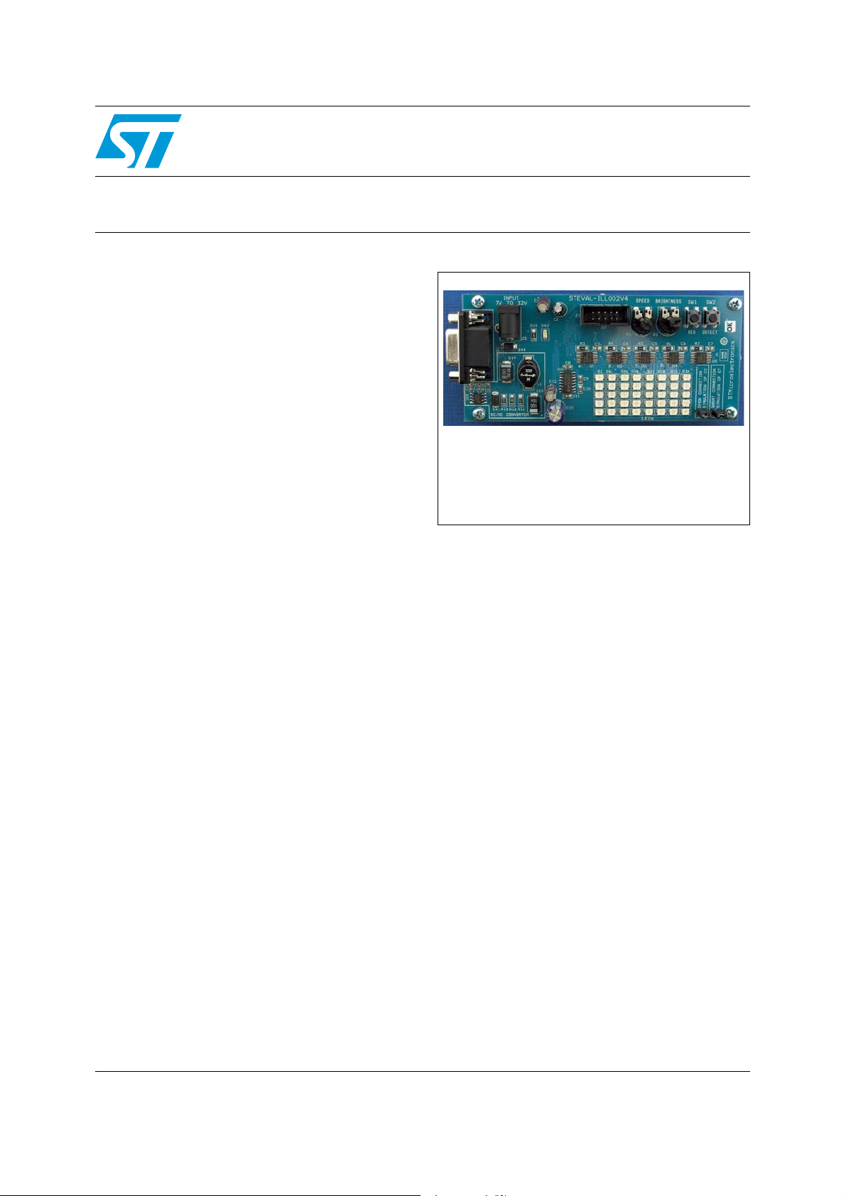
STEVAL-ILL002V4
demonstration board based on the STP08DP05
Data brief
This demonstration board provides a complete
solution for driving 40 high-brightness green
LEDs manufactured by Toshiba.
The high-brightness LEDs are arranged on the
board in a 5x8 matrix.
The matrix is driven by five 8-channel
STP08DP05 drivers which are controlled by the
ST7FLITE3x 8-bit microcontroller.
The innovative feature of STP08DP05 is the full
output error detection function, which checks the
status of the outputs without invasive tests (via
software).
STEVAL-ILL002V4
May 2009 Doc ID 15694 Rev 1 1/4
For further information contact your local STMicroelectronics sales office.
www.st.com
4
Circuit schematic STEVAL-ILL002V4
D1
D2
D2
D2
D8
D1
D4
D4
D9
D3
D2
D2
D5
D7
D2
D2
D6
D3
D1
D3
D2
D2
D3
D1
D3
D3
D3
D1
D3
D1
D3
D2
D3
D1
D1
D1
D2
D1
D3
Tx
Rx
SD
SD
RD
TD
RDI
TD
RE
RE
VC
VC
VC
VC
VC
VC
VC
VC
VC
VC
VC
VC
VC
FROM 7V UP TO 32V
INPUT
VOLTAGE
C1
22nFC1C1
22nF
C1
470nF
C1
470nF
P1
CONNECT
OR DB
P1
CONNECT
OR DB
D4
GREEN
LE
D4
GREEN
LE
10
10
D4
SM
AJ
33A-T
D4
SM
AJ
33A-T
L1
33uH
L1
33uH
100nFC3C3
100nF
GN
SD
CL
/L
Vd
16
R-
EXT
15
SD
14
/O
13
12
12
11
11
10
10
U1
ST
08DP05/
U1
ST
08DP05/
C4
100nF
C4
100nF
JP
JU
PER
JP
JU
PER
C1
10uF/35V
C1
10uF/35V
GN
SD
CL
/L
Vd
16
R-
EXT
15
SD
14
/O
13
12
12
11
11
10
10
U5
ST
08DP05/
U5
ST
08DP05/
1k
1k
10kR9R9
10k
1K
1K
R1
360R1R1
360
JP
JU
PER
JP
JU
PER
C1
10nFC1C1
10nF
SW
100n
100n
GN
SD
CL
/L
Vd
16
R-
EX
15
SD
14
/O
13
12
12
11
11
10
10
U3
ST
08DP05/
U3
ST
08DP05/
10
10
SW
D4
ST
PS340U
D4
ST
PS340U
10
10
C1
V+
C1
C2
C2
V-
T2OU
R2
IN
Vd
16
GN
15
T1OU
14
R1
IN
13
R1
OU
12
T1IN
11
T2IN
10
R2
OU
U6
ST
232ABN
U6
ST
232ABN
R1
6k
R1
6k
C1
10nF
C1
10nF
C1
100nF
C1
100nF
GN
SD
CL
/L
Vd
16
R-
EX
15
SD
14
/O
13
12
12
11
11
10
10
U4
ST
P08DP05/
U4
ST
P08DP05/
C2
220pF
C2
220pF
2.2uFC1C1
2.2uF
C1
100nFC1C1
100nF
C1
10nFC1C1
10nF
J5
CO
N3
J5
CO
N3
470nFC9C9
470nF
GN
SD
CL
/L
Vd
16
R-
EX
15
SD
14
/O
13
12
12
11
11
10
10
U2
ST
08DP05/
U2
ST
08DP05/
10
J1
IC
J1
IC
C8
470nF
C8
470nF
C1
2.2u
C1
2.2u
100nFC5C5
100nF
IO
L5970D
IO
L5970D
R1
4k
R1
4k
R1
2K
R1
2K
100nFC7C7
100nF
VO
UT
VI
NHI
U7
LE50/SO
U7
LE50/SO
R1
560R1R1
560
R5
1k
R5
1k
C2
100uF/16V
C2
100uF/16V
C2
220uF/25V
C2
220uF/25V
1k
1k
10
11
ST
lite3
U8
ST
lite3
U8
C2
10uF
C2
10uF
R7
1k
R7
1k
D1
C1
470nF
C1
470nF
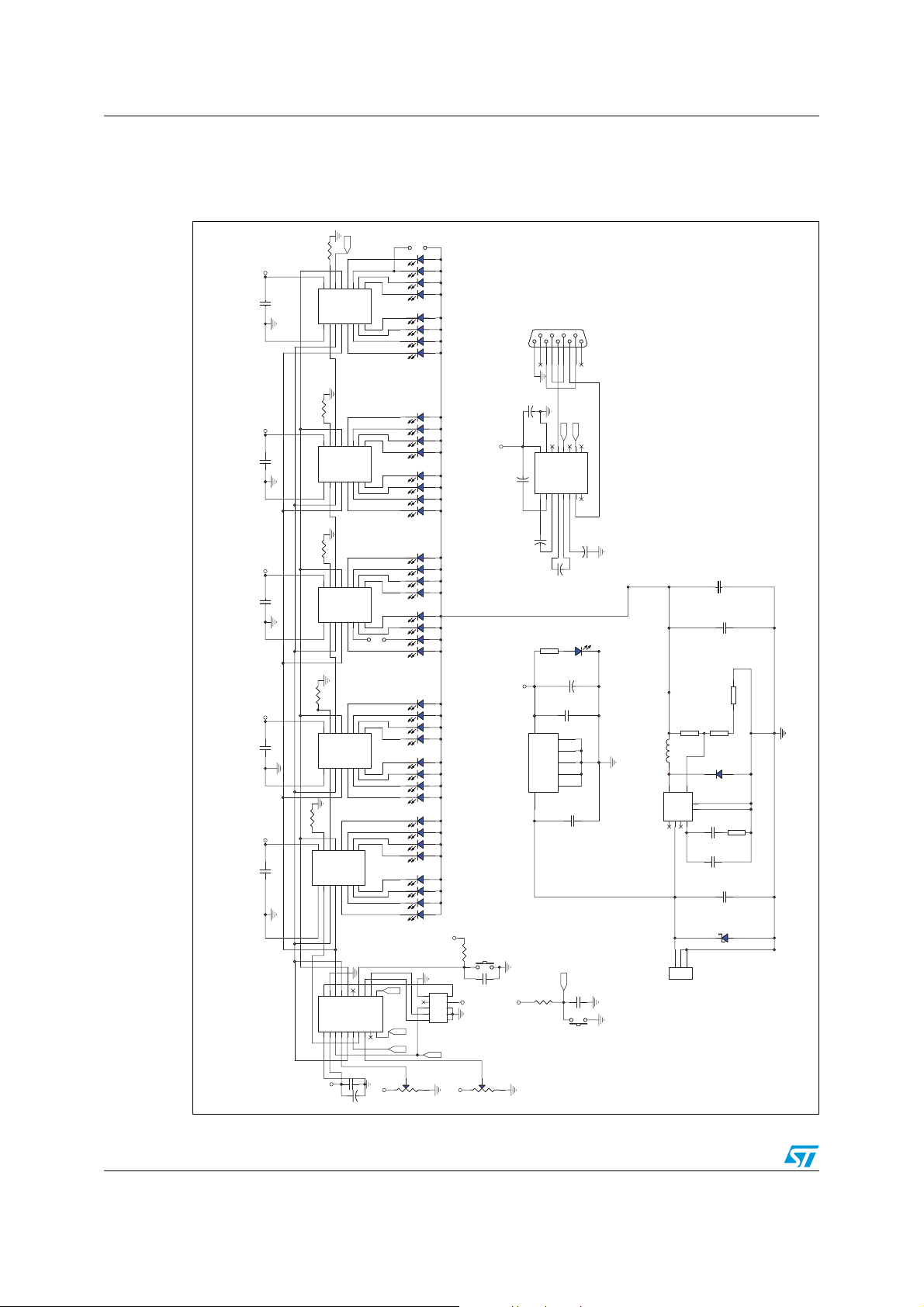
1 Circuit schematic
Figure 1. Schematic diagram
1
10
10
10
10
9
10uF
10uF
9
9
8
9
9
8
9
9
8
9
9
8
A
A
P08DP05/
P08DP05/
ST
ST
E
E
P08DP05/
P08DP05/
ST
ST
D
D
P08DP05/
P08DP05/
ST
ST
C
C
P08DP05/
P08DP05/
ST
ST
2
2
JP
JP
MPER
MPER
JU
JU
B
B
P08DP05/
P08DP05/
ST
ST
10
C
VC
1
JP
JP
MPER
MPER
0D4
JU
JU
9D1
D3
8D1
7D1
6D3
5D1
4D2
3D1
D3
2D2
1
0D2
D3
9D6
8D2
7D2
6 D2
D2
5D8
4D5
3 D3
2D1
1 D3
D2
0 D2
D2
9 D3
8D1D18
D1
1 2
7 D3
6 D3
5 D3
4 D2
3D1
2 D4
D1
1 D1
0 D3
D9
D7
D1
O
TD
7lite3
7lite3
ST
ST
I
0 RD
SD
2
R2R210
R2R210
13
1 2
9
9
OR DB
P1
P1
594837261
F
F
2
2
2.2u
2.2u
C1
C1
C
16
VC
d
Vd
470nF
470nF
1
1
C1
C1
+
C1
1
470nF
470nF
0
0
C1
C1
C
VC
1
B
UT
VO
LE50/SO
LE50/SO
N
VI
U7
U7
8
C
VC
k
k
2SWSW2
R8R810
R8R810
SW
4
4
C1
C1
J1
9
10
7
8
5
6
3
4
1
2
P J1
P
IC
IC
S
RE
k
k
C
VC
R1R110
R1R110
C
13
VC
10nF
10nF
k
k
2
R9R910k
10k
C
VC
OR DB
CONNECT
CONNECT
D
O
Rx
TD
RDI
D
Tx
14
12
9
15
13
11
10
T
T
T
D
IN
OU
OU
T1IN
T2IN
GN
R1
232ABN
232ABN
T1OU
R1
R2
ST
ST
T
-
+
-
IN
V+
C1
C2
C2
V-
T2OU
R2
U6
U6
7
3
4
5
2
6
8
470nF
470nF
C8
C8
1
1
220uF/25V
220uF/25V
C2
C2
+
1
1
R1
R1
21
5
1
7
3
682
4
123
VOLTAGE
INPUT
FROM 7V UP TO 32V
+
2
2
C2
C2
3
3
R1
2
2
8
8
6k
6k
R1
R1
1
1
D4
D4
8
8
22nF
22nF
C1
0
0
C2
C2
220pF
220pF
9
9
C1
C1
4
4
D4
D4
C9C9470nF
470nF
D
D
4
4
LE
LE
560
560
R1
2
2
GREEN
GREEN
D4
D4
C1C12.2uF
2.2uF
5
5
C1
C1
100nF
100nF
INHI
5
GNGND
7
GNGND
6
GNGND
3
GNGND
2
7
7
C1
100nF
100nF
S
RE
6
6
10nF
10nF
C1
1SWSW1
SW
33uH
33uH
L1
L1
5 L5970D
5 L5970D
IO
IO
N3
N3
CO
CO
J5
J5
0
3R7
3
SD
1k
1k
R7
14
16
15
13
d
O
Vd
EXT
SD
R-
D
I
K
GN
SD
CL
U5
U5
4
3
1
2
3
3
R6R61k
R6R61k
16
15
14
13
d
T
O
Vd
EX
SD
R-
D
I
K
U4
U4
GN
SD
CL
3
2
1
4
3
3
1k
1k
R5
R5
15
14
16
13
d
T
O
Vd
EX
SD
R-
D
I
K
U3
U3
GN
SD
CL
4
3
2
1
3
3
R4R41K
R4R41K
16
14
13
15
d
T
O
Vd
EX
SD
R-
D
I
K
U2
U2
GN
SD
CL
3
1
4
2
3
3
R3R31k
R3R31k
14
16
13
15
12
d
E
O
/O
Vd
EXT
SD
R-
D
I
K
E
U1
U1
GN
SD
CL
/L
1
3
4
2
20201919181817171616151514141313121211
U8
U8
123456789
C
VC
12
E
12
/O
E
/L
5566778
12
E
12
/O
E
/L
5566778
12
E
12
/O
E
/L
5566778
12
E
12
/O
E
/L
5566778
11
12
11
5566778
3
3
C1
C2
C2
11
10
11
11
10
11
11
10
11
11
10
11
9
10
10
8
10nF
10nF
+
+
CVC
C7C7100nF
100nF
CVC
F
F
C6C6100n
C6C6100n
C VC
VC
C5C5100nF
100nF
C
C4
C4
100nF
100nF
C VC
C3C3100nF
100nF
2/4 Doc ID 15694 Rev 1
2
2
2K
2K
PS340U
PS340U
ST
ST
0
0
R1
R1
10uF/35V
10uF/35V
100uF/16V
100uF/16V
R
R
33A-T
33A-T
AJ
AJ
SM
SM
360
360
7
7
4k
4k
AM03803v1

STEVAL-ILL002V4 Revision history
2 Revision history
Table 1. Document revision history
Date Revision Changes
11-May-2009 1 Initial release.
Doc ID 15694 Rev 1 3/4

STEVAL-ILL002V4
Please Read Carefully:
Information in this document is provided solely in connection with ST products. STMicroelectronics NV and its subsidiaries (“ST”) reserve the
right to make changes, corrections, modifications or improvements, to this document, and the products and services described herein at any
time, without notice.
All ST products are sold pursuant to ST’s terms and conditions of sale.
Purchasers are solely responsible for the choice, selection and use of the ST products and services described herein, and ST assumes no
liability whatsoever relating to the choice, selection or use of the ST products and services described herein.
No license, express or implied, by estoppel or otherwise, to any intellectual property rights is granted under this document. If any part of this
document refers to any third party products or services it shall not be deemed a license grant by ST for the use of such third party products
or services, or any intellectual property contained therein or considered as a warranty covering the use in any manner whatsoever of such
third party products or services or any intellectual property contained therein.
UNLESS OTHERWISE SET FORTH IN ST’S TERMS AND CONDITIONS OF SALE ST DISCLAIMS ANY EXPRESS OR IMPLIED
WARRANTY WITH RESPECT TO THE USE AND/OR SALE OF ST PRODUCTS INCLUDING WITHOUT LIMITATION IMPLIED
WARRANTIES OF MERCHANTABILITY, FITNESS FOR A PARTICULAR PURPOSE (AND THEIR EQUIVALENTS UNDER THE LAWS
OF ANY JURISDICTION), OR INFRINGEMENT OF ANY PATENT, COPYRIGHT OR OTHER INTELLECTUAL PROPERTY RIGHT.
UNLESS EXPRESSLY APPROVED IN WRITING BY AN AUTHORIZED ST REPRESENTATIVE, ST PRODUCTS ARE NOT
RECOMMENDED, AUTHORIZED OR WARRANTED FOR USE IN MILITARY, AIR CRAFT, SPACE, LIFE SAVING, OR LIFE SUSTAINING
APPLICATIONS, NOR IN PRODUCTS OR SYSTEMS WHERE FAILURE OR MALFUNCTION MAY RESULT IN PERSONAL INJURY,
DEATH, OR SEVERE PROPERTY OR ENVIRONMENTAL DAMAGE. ST PRODUCTS WHICH ARE NOT SPECIFIED AS "AUTOMOTIVE
GRADE" MAY ONLY BE USED IN AUTOMOTIVE APPLICATIONS AT USER’S OWN RISK.
Resale of ST products with provisions different from the statements and/or technical features set forth in this document shall immediately void
any warranty granted by ST for the ST product or service described herein and shall not create or extend in any manner whatsoever, any
liability of ST.
ST and the ST logo are trademarks or registered trademarks of ST in various countries.
Information in this document supersedes and replaces all information previously supplied.
The ST logo is a registered trademark of STMicroelectronics. All other names are the property of their respective owners.
© 2009 STMicroelectronics - All rights reserved
Australia - Belgium - Brazil - Canada - China - Czech Republic - Finland - France - Germany - Hong Kong - India - Israel - Italy - Japan -
STMicroelectronics group of companies
Malaysia - Malta - Morocco - Philippines - Singapore - Spain - Sweden - Switzerland - United Kingdom - United States of America
www.st.com
4/4 Doc ID 15694 Rev 1
 Loading...