

Hi-Rel NPN and PNP bipolar transistor 60 V, 0.8 A
3
2
1
4
5
6
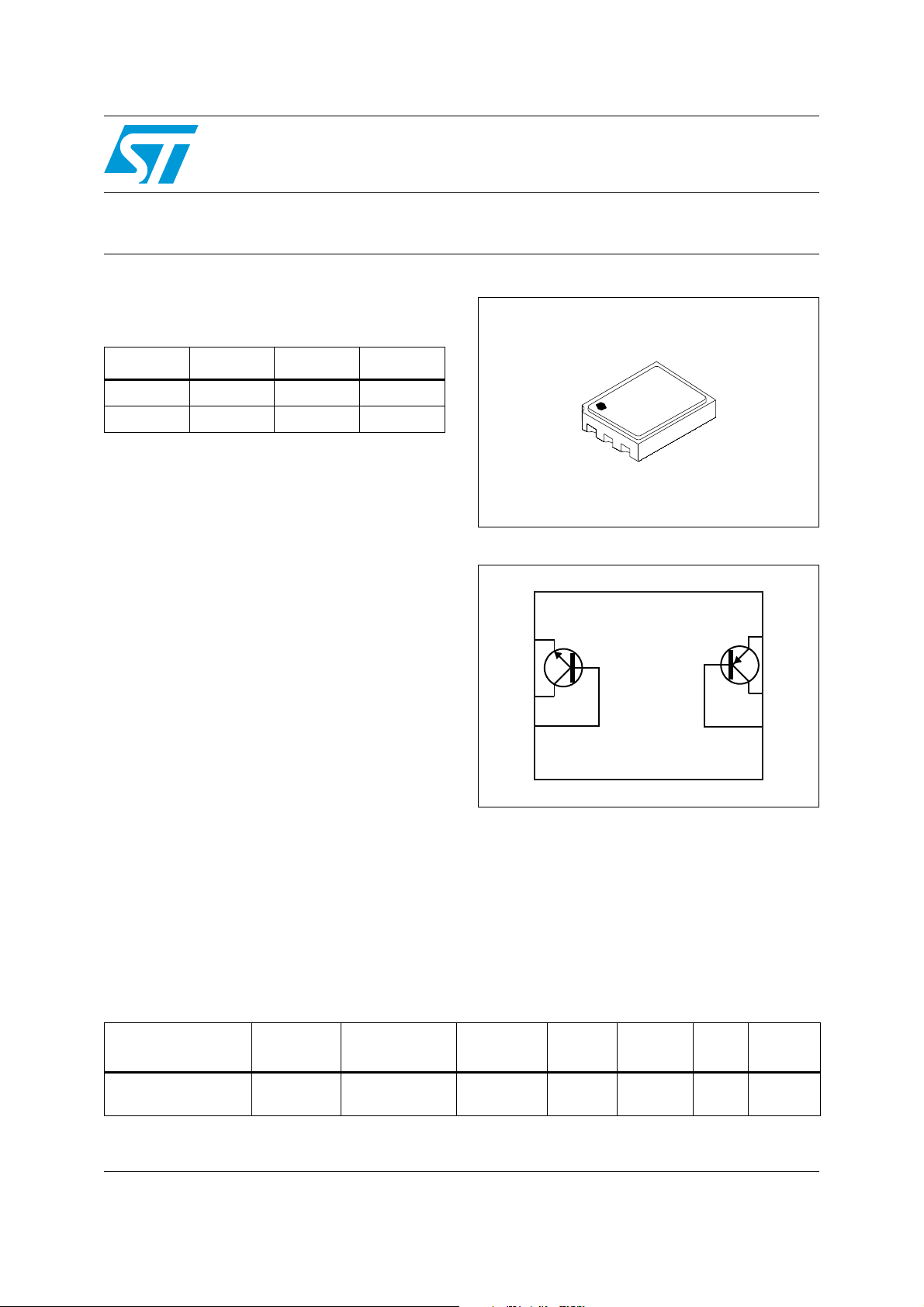
LCC-6
Features
Polarity BV
NPN 60 V 0.8 A 160
PNP -60 V - 0.8 A 160
1. @ Ic = 1 A and VCE = 2 V.
■ Very low collector-emitter saturation voltage
■ High current gain characteristic
■ Fast-switching speed: FT= 130 MHz
■ Hermetic package
■ Manufactured according to ESCC 5000
CEO
IC (max) h
specifications
■ 100 krad low dose rate
FE
(1)
2ST3360
Datasheet — production data
Figure 1. Internal schematic diagram
Applications
■ Power MOSFET drivers
Description
The 2ST3360 power bipolar transistor is a fast
dual complementary device (NPN and PNP)
housed in a single LCC-6 hermetic Hi-Rel
package, specifically designed for aerospace HiRel applications. Its radiation hardness allows key
parameters such as gain and leakage current to
stay at best-in-class post irradiation levels. ST
proprietary technology also results in a high
degree of electrical performance for both
transistors in the pair. The high switching
performance of each make this device particularly
suitable for power MOSFET driver applications.
number
(1)
Quality level
Engineering
model
Table 1. Device summary
Order code
2ST3360U1 -
ESCC part
Radiation
level
- LCC-6 Gold 0.20 g -
Package
Lead
finish
Mass EPPL
1. Contact ST sales office for information about the specific conditions for tape and reel packing.
May 2012 Doc ID 022014 Rev 3 1/11
This is information on a product in full production.
www.st.com
11

Contents 2ST3360
Contents
1 Absolute maximum ratings . . . . . . . . . . . . . . . . . . . . . . . . . . . . . . . . . . . 3
2 Pin configuration . . . . . . . . . . . . . . . . . . . . . . . . . . . . . . . . . . . . . . . . . . . . 4
3 Electrical characteristics . . . . . . . . . . . . . . . . . . . . . . . . . . . . . . . . . . . . . 5
3.1 Test circuits . . . . . . . . . . . . . . . . . . . . . . . . . . . . . . . . . . . . . . . . . . . . . . . . . 6
4 Package mechanical data . . . . . . . . . . . . . . . . . . . . . . . . . . . . . . . . . . . . . 7
5 Order code . . . . . . . . . . . . . . . . . . . . . . . . . . . . . . . . . . . . . . . . . . . . . . . . . 9
6 Revision history . . . . . . . . . . . . . . . . . . . . . . . . . . . . . . . . . . . . . . . . . . . 10
2/11 Doc ID 022014 Rev 3
2ST3360 Absolute maximum ratings
1 Absolute maximum ratings
Table 2. Absolute maximum ratings
Val ue
Symbol Parameter
NPN PNP
Unit
V
V
V
P
CBO
CEO
EBO
I
I
CM
I
I
BM
TOT
T
stg
T
Collector-base voltage (IE = 0) 60 -60 V
Collector-emitter voltage (IB = 0) 60 -60 V
Emitter-base voltage (IC = 0) 6 -6 V
Collector current 0.8 -0.8 A
C
Collector peak current (tP < 5 ms) 4 -4 A
Base current 0.2 -0.2 A
B
Base peak current (tP < 5 ms) 0.4 -0.4 A
Total dissipation at T
= 25 °C 1.4 W
amb
Storage temperature -65 to 200 °C
Max. operating junction temperature 200 °C
J
Table 3. Thermal data
Symbol Parameter Value Unit
R
thJA
Thermal resistance junction-ambient max 125 °C/W
Note: Mounted on a 15 x 15 x 0.6 mm ceramic substrate.
Doc ID 022014 Rev 3 3/11
Pin configuration 2ST3360
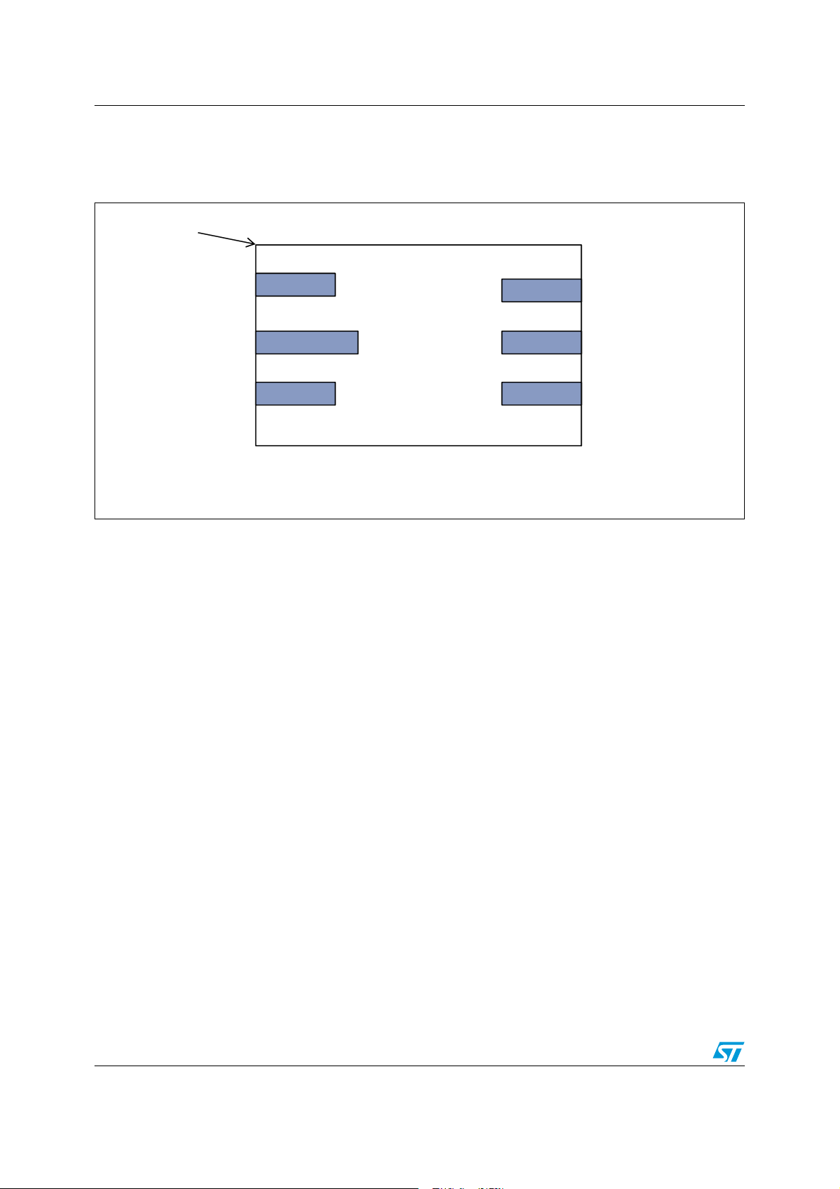
.0.%MITTER
.0.#OLLECTROR
.0."ASE
0.0"ASE
0.0#OLLECTOR
0.0%MITTER
-ETALLIZED CORNER
"OTTOM VIEW PADSIDE
!-V
2 Pin configuration
Figure 2. Pin connections
4/11 Doc ID 022014 Rev 3

2ST3360 Electrical characteristics
3 Electrical characteristics
T
= 25 °C; unless otherwise specified.
CASE
Table 4. Electrical characteristics for NPN
Symbol Parameter Test conditions Min. Typ. Max. Unit
I
I
V
V
CE(sat)
h
CBO
EBO
BE(on)
(1)
FE
Collector cut-off current
(I
= 0)
E
Emitter cut-off current
(I
= 0)
C
Base-emitter on voltage VCE = 2 V IC = 100 mA 650 mV
Collector-emitter
(1)
saturation voltage
DC current gain
= 60 V
V
CB
V
= 60 V, TA = 110 °C
CB
= 6 V 100 nA
V
EB
= 0.8 A IB = 40 mA
I
C
IC = 2 A IB = 100 mA
IC = 100 mA_ V
IC = 1 A _V
CE
CE
= 2 V
= 2 V
160 400
250
550
80
10010nA
Resistive load
t
t
f
1. Pulse test: pulse duration ≤ 300 µs, duty cycle ≤ 2%
Table 5. Electrical characteristics for PNP
Delay time
d
Rise time
t
r
Storage time
s
Fall time
t
f
Transition frequency IC = 0.1 A __ V
T
I
= 2 A V
C
I
= - I
B(on)
V
= - 5 V
BE(off)
B(off)
= 10 V
CC
= 200 mA
= 10 V 130 MHz
CE
(1)
20
70
830
67
Symbol Parameter Test conditions Min. Typ. Max. Unit
µA
mV
ns
ns
ns
ns
I
I
V
V
CE(sat)
h
CBO
EBO
BE(on)
(1)
FE
Collector cut-off current
(I
= 0)
E
Emitter cut-off current
(I
= 0)
C
Base-emitter on voltage VCE = 2 V IC = 100 mA 650 mV
Collector-emitter
(2)
saturation voltage
DC current gain
= 60 V
V
CB
V
= 60 V, TA = 110 °C
CB
= 6 V 100 nA
V
EB
= 0.8 A IB = 40 mA
I
C
I
= 2 A IB = 100 mA
C
IC = 100 mA_ V
IC = 1 A _ V
Resistive load
t
t
f
1. For PNP type, voltage and current values are negative.
2. Pulse test: pulse duration ≤ 300 µs, duty cycle ≤ 2%
Delay time
d
Rise time
t
r
Storage time
s
Fall time
t
f
Transition frequency IC = 0.1 A __ V
T
I
= 2 A V
C
I
= - I
B(on)
V
= - 5 V
BE(off)
Doc ID 022014 Rev 3 5/11
B(off)
10010nA
250
550
= 2 V
CE
= 2 V80160 400
CE
= 10 V
CC
= 200 mA
22
54
360
42
= 10 V 130 MHz
CE
µA
mV
ns
ns
ns
ns

Electrical characteristics 2ST3360
3.1 Test circuits
Figure 3. Resistive load switching for NPN
1. Fast electronic switch
2. Non-inductive resistor
Figure 4. Resistive load switching for PNP
1. Fast electronic switch
2. Non-inductive resistor
6/11 Doc ID 022014 Rev 3

2ST3360 Package mechanical data
4 Package mechanical data
In order to meet environmental requirements, ST offers these devices in different grades of
ECOPACK
specifications, grade definitions and product status are available at: www.st.com.
ECOPACK
®
packages, depending on their level of environmental compliance. ECOPACK®
®
is an ST trademark.
Doc ID 022014 Rev 3 7/11

Package mechanical data 2ST3360
7098021_B
A
C
F
G
DD1
L
r
N
N1
M
I
E
N2
Table 6. Ceramic leadless chip carrier 6 mechanical data
mm. inch.
Dim. Min. Typ. Max. Min. Typ. Max.
A 1.53 1.96 .060 .077
C 0.78 0.89 0.99 .031 .035 .039
D 1.52 1.65 1.78 .060 .065 .070
E 1.24 1.40 1.55 .049 .055 .059
F 5.77 5.84 5.92 .227 .230 .233
G 4.19 4.31 4.45 .165 .170 .175
I 6.10 6.22 6.35 .240 .245 .250
L 0.56 0.63 0.71 .022 .025 .028
M 3.86 3.94 4.01 .152 .155 .158
N 1.14 1.27 1.40 .045 .050 .055
N1 2.41 2.54 2.67 .095 .100 .105
N2 0.64 0.89 1.14 .025 .035 .045
r 0.23 .009
D1 2.08 2.28 2.49 .082 .090 .098
Figure 5. Dimensions for ceramic leadless chip carrier 6
8/11 Doc ID 022014 Rev 3

2ST3360 Order code
5 Order code
Quality
level
model
(1)
Radiation
level
- LCC-6 Gold 2ST3360U1 - Wafflepack
Package
Lead
finish
Marking EPPL Packing
Table 7. Ordering information
ESCC
Order code
2ST3360U1 -
1. Contact an ST sales office for information regarding the specific conditions for tape and reel packing.
part
number
Engineering
Doc ID 022014 Rev 3 9/11

Revision history 2ST3360
6 Revision history
Table 8. Document revision history
Date Revision Changes
18-Jul-2011 1 Initial release.
01-Feb-2012 2 Section 2. inserted.
04-May-2012 3
Updated V
characteristics for NPN and Table 5: Electrical characteristics for
PNP.
value and test condition in Table 4: Electrical
CE(sat)
10/11 Doc ID 022014 Rev 3

2ST3360
Please Read Carefully:
Information in this document is provided solely in connection with ST products. STMicroelectronics NV and its subsidiaries (“ST”) reserve the
right to make changes, corrections, modifications or improvements, to this document, and the products and services described herein at any
time, without notice.
All ST products are sold pursuant to ST’s terms and conditions of sale.
Purchasers are solely responsible for the choice, selection and use of the ST products and services described herein, and ST assumes no
liability whatsoever relating to the choice, selection or use of the ST products and services described herein.
No license, express or implied, by estoppel or otherwise, to any intellectual property rights is granted under this document. If any part of this
document refers to any third party products or services it shall not be deemed a license grant by ST for the use of such third party products
or services, or any intellectual property contained therein or considered as a warranty covering the use in any manner whatsoever of such
third party products or services or any intellectual property contained therein.
UNLESS OTHERWISE SET FORTH IN ST’S TERMS AND CONDITIONS OF SALE ST DISCLAIMS ANY EXPRESS OR IMPLIED
WARRANTY WITH RESPECT TO THE USE AND/OR SALE OF ST PRODUCTS INCLUDING WITHOUT LIMITATION IMPLIED
WARRANTIES OF MERCHANTABILITY, FITNESS FOR A PARTICULAR PURPOSE (AND THEIR EQUIVALENTS UNDER THE LAWS
OF ANY JURISDICTION), OR INFRINGEMENT OF ANY PATENT, COPYRIGHT OR OTHER INTELLECTUAL PROPERTY RIGHT.
UNLESS EXPRESSLY APPROVED IN WRITING BY TWO AUTHORIZED ST REPRESENTATIVES, ST PRODUCTS ARE NOT
RECOMMENDED, AUTHORIZED OR WARRANTED FOR USE IN MILITARY, AIR CRAFT, SPACE, LIFE SAVING, OR LIFE SUSTAINING
APPLICATIONS, NOR IN PRODUCTS OR SYSTEMS WHERE FAILURE OR MALFUNCTION MAY RESULT IN PERSONAL INJURY,
DEATH, OR SEVERE PROPERTY OR ENVIRONMENTAL DAMAGE. ST PRODUCTS WHICH ARE NOT SPECIFIED AS "AUTOMOTIVE
GRADE" MAY ONLY BE USED IN AUTOMOTIVE APPLICATIONS AT USER’S OWN RISK.
Resale of ST products with provisions different from the statements and/or technical features set forth in this document shall immediately void
any warranty granted by ST for the ST product or service described herein and shall not create or extend in any manner whatsoever, any
liability of ST.
ST and the ST logo are trademarks or registered trademarks of ST in various countries.
Information in this document supersedes and replaces all information previously supplied.
The ST logo is a registered trademark of STMicroelectronics. All other names are the property of their respective owners.
© 2012 STMicroelectronics - All rights reserved
STMicroelectronics group of companies
Australia - Belgium - Brazil - Canada - China - Czech Republic - Finland - France - Germany - Hong Kong - India - Israel - Italy - Japan -
Malaysia - Malta - Morocco - Philippines - Singapore - Spain - Sweden - Switzerland - United Kingdom - United States of America
www.st.com
Doc ID 022014 Rev 3 11/11
 Loading...