

Page 1
Working Instruction, Electrical
Working Instruction, Electrical
Applicable for V800/ 802se
INDEX
1 LEAD FREE SOLDERING..........................................................................................................................................2
1.1 INTRODUCTION.........................................................................................................................................................2
1.1.1 Environment.....................................................................................................................................................2
1.1.2 Soldering temperature .....................................................................................................................................3
2 BGA EQUIPMENT REFLOW PROFILES ...............................................................................................................5
2.1 TEMPERATURE MEASUREMENT ................................................................................................................................5
2.1.1 Reflow Profiles ................................................................................................................................................6
3 REPLACEMENT OF PARTS......................................................................................................................................7
3.1 EQUIPMENT ..............................................................................................................................................................7
3.2 INSTRUCTION HOW REPLACING PARTS ......................................................................................................................7
3.2.1 External Antenna Connector ...........................................................................................................................8
3.2.2 30 PIN BTB Female Connector, behind the System Connector.......................................................................8
3.2.3 30 PIN BTB Female Connector.......................................................................................................................9
3.2.4 50 PIN BTB Female Connector.......................................................................................................................9
3.2.5 Battery Connector..........................................................................................................................................10
3.2.6 USB Connector ..............................................................................................................................................10
3.2.7 MS Duo and SIM Reader...............................................................................................................................11
3.2.8 Hall Element..................................................................................................................................................11
3.2.9 IrDa Module ..................................................................................................................................................12
3.2.10 Coax Connector.............................................................................................................................................12
4 REVISION HISTORY................................................................................................................................................13
3/000 21-2/FEA 209544/88 C
Company Internal
Sony Ericsson Mobile Communications AB
Approved according to 000 21-LXE 107 42/1
Page 2
Working Instruction, Electrical
1 Lead free soldering
In this chapter there is an introduction that will explain what is important to think about when
working with the product.
1.1 Introduction
This products soldering process is lead-free. It is important that all contact surfaces are kept
clean from dirt and hand-grease. During electrical repair, it is critical to make sure that no
lead is introduced.
1.1.1 Environment
The introduction of the environment is as follow:
Information text
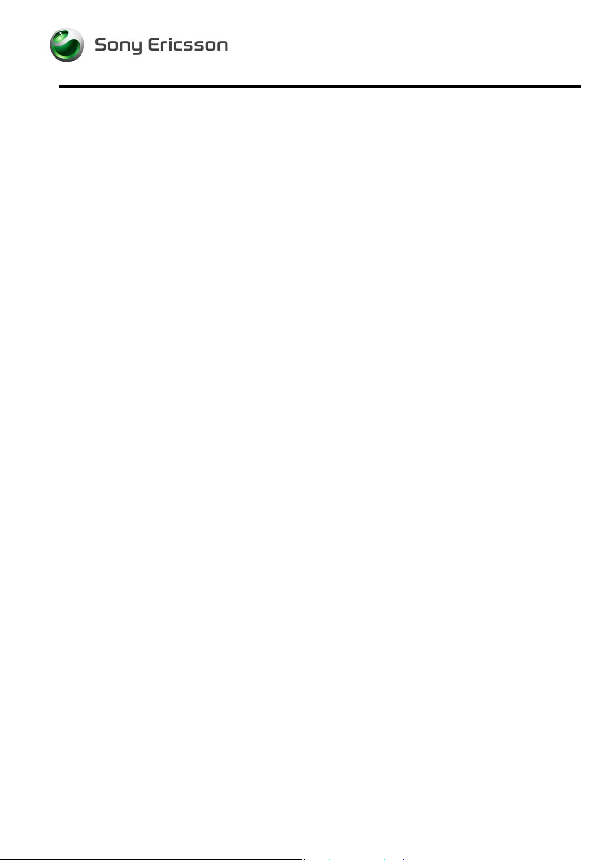
1 This symbol indicates that the product is lead
free.
2 All lead free PCB will be marked with this
symbol, according to the arrow.
3/000 21-2/FEA 209544/88 C
Company Internal
Sony Ericsson Mobile Communications AB
2(13)
Page 3
Working Instruction, Electrical
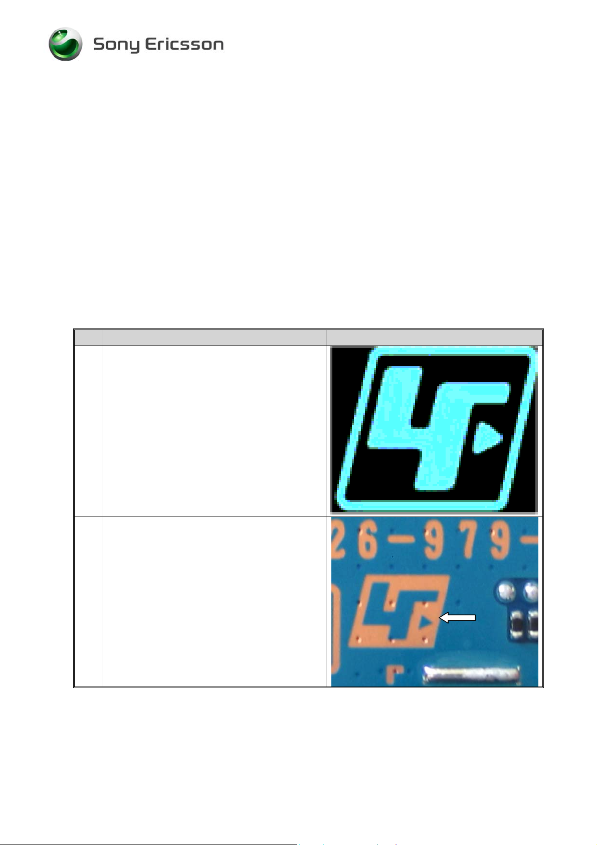
Information text
3 A lead free work area must be set up that is
completely separated from work areas that are
used to make leaded repairs.
The lead-free work area must also be clearly
marked with the lead free symbol as shown in
the figure beside.
The items in this table must remain lead free.
They must be adequately marked to make their
lead free status clearly and easily recognized.
1.1.2 Soldering temperature
The characteristics of Lead Free Solder paste is:
• High melting point (Typically 220°C)
• Low wet ability
• High surface tension
• Difficult to spread
Recommended tip temperature 370°C
When servicing PCB´s that is produced with Lead Free Solder paste this paste must
Otherwise there is a high risk for unreliable soldering joints.
A smaller introduction of the solder temperature, with pictures, is as follow:
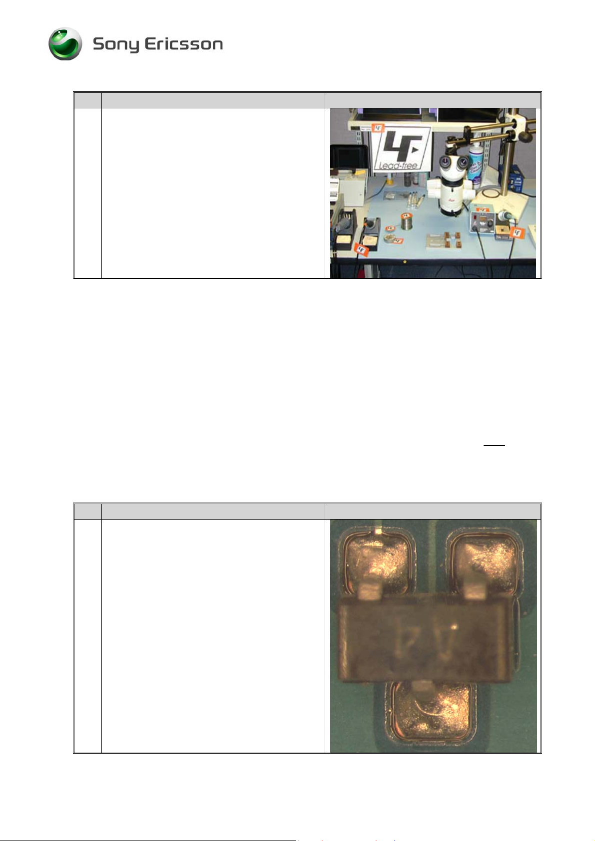
Information text
1 Lead Free Solder joints are more difficult to
inspect because they do not have shiny surfaces
like leaded solders joints.
Lead Free Solder does not flow as well as
leaded solder. Some of the solder pad area may
remain exposed.
The picture shows an example of Lead Free
Solders joints.
be used.
3/000 21-2/FEA 209544/88 C
Company Internal
Sony Ericsson Mobile Communications AB
3(13)
Page 4
Working Instruction, Electrical
Information text
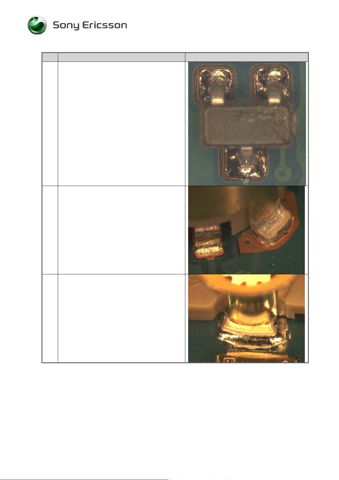
2 The picture shows an example of solder joints
with lead.
3 The picture shows an example of lead free
solder joints.
4 The picture shows an example of solder joints
with lead.
3/000 21-2/FEA 209544/88 C
Company Internal
Sony Ericsson Mobile Communications AB
4(13)
Page 5

Working Instruction, Electrical
2 BGA Equipment reflow profiles
This chapter contains recommendations for reflow profile for mobile phones and similar
products. This is only general recommendation and considerations have to be taken for every
single product. The solder paste is secondary but could also affect the parameters.
In this document one alloy is specified:
SnAgCu (Lead free) melting point 217°C
2.1 Temperature measurement
At least 4 probes should be used:
They should be placed on components with the highest and lowest thermal mass.
They shall be located in the beginning, in the middle and at the end of the board/panel.
They are recommended to be soldered on the board but glue and capton tape could also be
used if necessary.
At least one probe shall be placed in the air or on top of a component.
These values are strongly depending on the BGA replacement equipment.
Nozzle type will be chosen after the outer size of the actual component. Make sure the nozzle
does not affect any near placed components.
NOTE:
These values are recommendations and may have to be changed depending on the type of
equipment.
The maximum temperature for any component must not exceed 250C.
3/000 21-2/FEA 209544/88 C
Company Internal
Sony Ericsson Mobile Communications AB
5(13)
Page 6

Working Instruction, Electrical
2.1.1 Reflow Profiles
Sn/Ag/Cu (Lead free)
290
250
200
150
Temperature [ºC]
100
50
0
Preheat zone
Reflow zone
Cooling zone
40 80 120 160 200 240 280
Time [Seconds]
260°C
245°C
235°C
Ramp rate < 4°C/sec
Ramp rate cooling zone < 6°C/sec
Time above liquids 60-150 sec
Minimum temperature 235°C
Maximum temperature 245°C or 260°C* for 10 sec
Total time Appr. 4-7 min
* The higher temperature in case the board has extremely high ∆T.
3/000 21-2/FEA 209544/88 C
Company Internal
Sony Ericsson Mobile Communications AB
6(13)
Page 7

Working Instruction, Electrical
3 Replacement of parts
In this chapter there is an introduction that explains what equipment to use when replacing
parts in the product and also how to replace these parts. When doing these replacing
procedures it is important it is important that all contact surfaces are kept clean from dirt and
hand-grease.
3.1 Equipment
The list of equipment to use is as follow:
Dentist hook •
•
ESD-gloves (cotton gloves)
•
ESD-wristband
•
Soldering tool
•
Hot air soldering station
•
BGA replacement equipment
•
Pair of tweezers
•
Solder cleaning wiper (Tin wick)
•
Solder paste Lead free (SN 96% Ag 3.5% Cu 0.5%) Use the soldering tip only for lead
free solder paste.
•
Flux, RMA No-clean flux
•
Cutting pliers
•
Shield fence pliers NTZ 112 537
3.2 Instruction how replacing parts
Before it is possible to replace any of these parts the phone has to be dissembled as described
in Working Instruction 3/00021-2/FEA 209 544/88 PA1
After the part is replaced it is important to assemble the phone according to the Working
Instruction 3/00021-2/FEA 209 544/88 PA1.
3/000 21-2/FEA 209544/88 C
Company Internal
Sony Ericsson Mobile Communications AB
7(13)
Page 8

Working Instruction, Electrical
3.2.1 External Antenna Connector
This is the instruction how to replace the External Antenna Connector:
Step-by-Step Instructions
1 Use BGA Repair Equipment to replace the
Antenna Connector, which is located accordig to
the arrow.
3.2.2 30 PIN BTB Female Connector, behind the System Connector
This is the instruction how to replace the 30 PIN BTB Female Connector:
Step-by-Step Instructions
1 NOTE!
The 30 PIN BTB Female Connector is located
behind the System Connector, according to the
arrow (1).
Remove the System Connector.
NOTE!
The Light Gasket is located according to the
arrow (2).
Be careful not to damage other components.
Use a dentist hook to remove the Light Gasket.
Clean the surface with Isopropyl alcohol.
Use BGA Repair Equipment to replace the
Antenna 30 PIN BTB Female Connector to the
right position, according to the arrow (3).
Apply a new Sealing Gasket.
2
3
1
3/000 21-2/FEA 209544/88 C
Company Internal
Sony Ericsson Mobile Communications AB
8(13)
Page 9

Working Instruction, Electrical
3.2.3 30 PIN BTB Female Connector
This is the instruction how to replace the 30 PIN BTB Female Connector:
Step-by-Step Instructions
1 NOTE!
The Sealing Gasket is located according to the
arrow (1).
Be careful not to damage other components.
Use a dentist hook to remove the Sealing
Gasket.
Clean the surface with Isopropyl alcohol.
Use the BGA Repair Equipment to replace the
antenna 30 PIN BTB Female Connector to the
right position, according to the arrow (2).
Apply a new Sealing Gasket.
1
2
3.2.4 50 PIN BTB Female Connector
This is the instruction how to replace the 50 PIN BTB Female Connector:
Step-by-Step Instructions
1 NOTE!
The Sealing Gasket is located according to the
arrow (1).
Be careful not to damage other components.
Usa a dentist hook to remove the Sealing
Gasket.
Clean the surface with Isopropyl alcohol.
Use the BGA Repair Equipment to replace the
antenna 30 PIN BTB Female Connector to the
right position, according to the arrow (2).
Apply a new Sealing Gasket.
1
2
3/000 21-2/FEA 209544/88 C
Company Internal
Sony Ericsson Mobile Communications AB
9(13)
Page 10

Working Instruction, Electrical
3.2.5 Battery Connector
This is the instruction how to replace the Battery Connector:
Step-by-Step Instructions
1 NOTE!
The Battery Connector is located according to
the arrow.
Use BGA Repair Equipment to remove and
assemble a new Battery Connector.
3.2.6 USB Connector
This is the instruction how to replace the USB Connector:
Step-by-Step Instructions
1 NOTE!
The USB Connector is located according to the
arrow.
Use a soldering iron to replace USB Connector.
3/000 21-2/FEA 209544/88 C
Company Internal
Sony Ericsson Mobile Communications AB
10(13)
Page 11

Working Instruction, Electrical
3.2.7 MS Duo and SIM Reader
This is the instruction how to replace the MS Duo and SIM reader:
Step-by-Step Instructions
1 NOTE!
The MS Duo and SIM Reader is located
according to the arrow.
Use a soldering iron replace the MS Duo and
SIM Reader.
3.2.8 Hall Element
This is the instruction how to replace the Hall element:
Step-by-Step Instructions
1 NOTE!
The Hall Element is located according to the
arrow.
Use a soldering iron to replace the Hall Element.
3/000 21-2/FEA 209544/88 C
Company Internal
Sony Ericsson Mobile Communications AB
11(13)
Page 12

Working Instruction, Electrical
3.2.9 IrDa Module
This is the instruction how to replace the IrDa Module:
Step-by-Step Instructions
1 NOTE!
The IrDA Module is located according to the
arrow.
Use a soldering iron to replace the IrDa Module.
3.2.10 Coax Connector
This is the instruction how to replace the Coax Connector:
1 NOTE!
The Coax Connector is located according to the
arrow.
Use a soldering iron to replace the Coax
Connector.
3/000 21-2/FEA 209544/88 C
Company Internal
Sony Ericsson Mobile Communications AB
12(13)
Page 13

Working Instruction, Electrical
4 Revision History
The list over the revision history is as follows:
Rev. Date Changes / Comments
A 2004-11-17 First Release
B 2004-12-13 Due to system problem
C 2004-12-15 Due to system problem
3/000 21-2/FEA 209544/88 C
Company Internal
Sony Ericsson Mobile Communications AB
13(13)
 Loading...