

Sony ZSX-1 Service manual
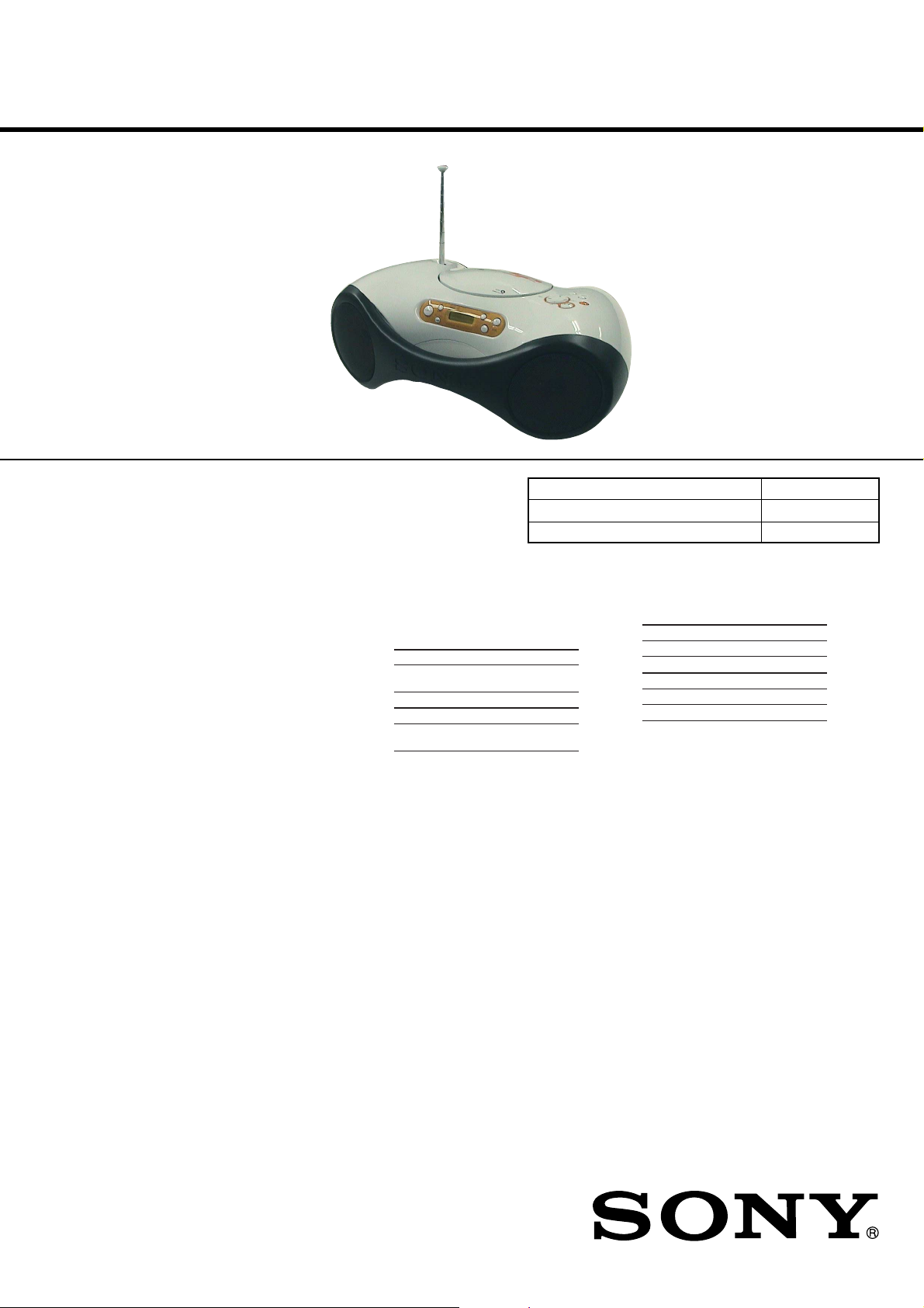
ZS-X1
SERVICE MANUAL
Ver 1.2 2003.07
SPECIFICATIONS
AUDIO POWER SPECIFICATIONS
(US model only)
POWER OUTPUT AND TOTAL
HARMONIC DISTORTION
With 3.2-ohm loads, both channels driven
from 150 - 10 000 Hz; rated 1.8 W per
channel-minimum RMS power, with no
more than 10 % total harmonic distortion
in AC operation.
Other specifications
CD player section
System
Compact disc digital audio system
Laser diode properties
Material: GaAlAs
Wave length: 780 nm
Emission duration: Continuous
Laser output: Less than 44.6 µW
(This output is the value measured at a distance
of about 200 mm from the objective lens surface
on the optical pick-up block with 7 mm
aperture.)
Spindle speed
200 r/min (rpm) to 500 r/min (rpm)
(CLV)
Number of channels
2
Frequency response
20 - 20 000 Hz +0/–1 dB
Wow and flutter
Below measurable limit
Radio section
Frequency range
FM: 87.5 - 108 MHz
AM: 530 - 1 710 kHz (US, Canadian models)
European model
MW 531 - 1 611 kHz (9 kHz step)
LW 153 - 279 kHz
Other models
AM 531 - 1 611 kHz (9 kHz step)
Antennas
FM: Telescopic antenna
AM/MW/LW: Built-in ferrite bar antenna
General
Speaker
Full range: 10 cm dia., 3.2 ohms, cone type (2)
Outputs
Headphones jack (stereo minijack)
For 16 - 64 ohms impedance headphones
Power output
2.3 W + 2.3 W (at 3.2 ohms, 10% harmonic
distortion)
Power requirements
DC IN 9V jack accepts:
Supplied AC power adaptor for use with
120 V AC, 60 Hz (US, Canadian)
220 V AC, 60 Hz (Korean)
230 V AC, 50 Hz (Australian)
240 V AC, 50 Hz (Others)
9 V DC, 6 size D (R20) batteries
530 - 1 610 kHz (10 kHz step)
530 - 1 610 kHz (10 kHz step)
US Model
Canadian Model
AEP Model
UK Model
E Model
Austr alian Model
Model Name Using Similar Mechanism NEW
CD Mechanism Type KSM-213RAP
Optical Pick-up Name KSS-213R
Battery life
For personal audio system:
CD playback
Sony R20P: approx. 7.5 h
Sony alkaline LR20: approx. 14 h
Radio play
Sony R20P: approx. 11 h
Sony alkaline LR20: approx. 24 h
Dimensions
Approx. 430 × 175 × 288 mm (w/h/d)
7
⁄8 × 11 3⁄8 inches) (incl. projecting parts)
(17 × 6
Mass
Approx. 3.5 kg (7 lb. 11 oz) (incl. batteries)
Supplied accessory
AC power adaptor(1)
Design and specifications are subject to change
without notice.
9-877-101-03 Sony Corporation
2003G05-1 Personal Audio Company
C 2003.07 Published by Sony Engineering Corporation
PERSONAL AUDIO SYSTEM
ZS-X1
Notes on chip component replacement
•Never reuse a disconnected chip component.
• Notice that the minus side of a tantalum capacitor may be damaged by heat.
Flexible Circuit Board Repairing
•Keep the temperature of the soldering iron around 270 ˚C during repairing.
• Do not touch the soldering iron on the same conductor of the
circuit board (within 3 times).
• Be careful not to apply force on the conductor when soldering
or unsoldering.
SAFETY CHECK-OUT
After correcting the original service problem, perform the following safety check before releasing the set to the customer:
Check the antenna terminals, metal trim, “metallized” knobs,
screws, and all other exposed metal parts for AC leakage.
Check leakage as described below.
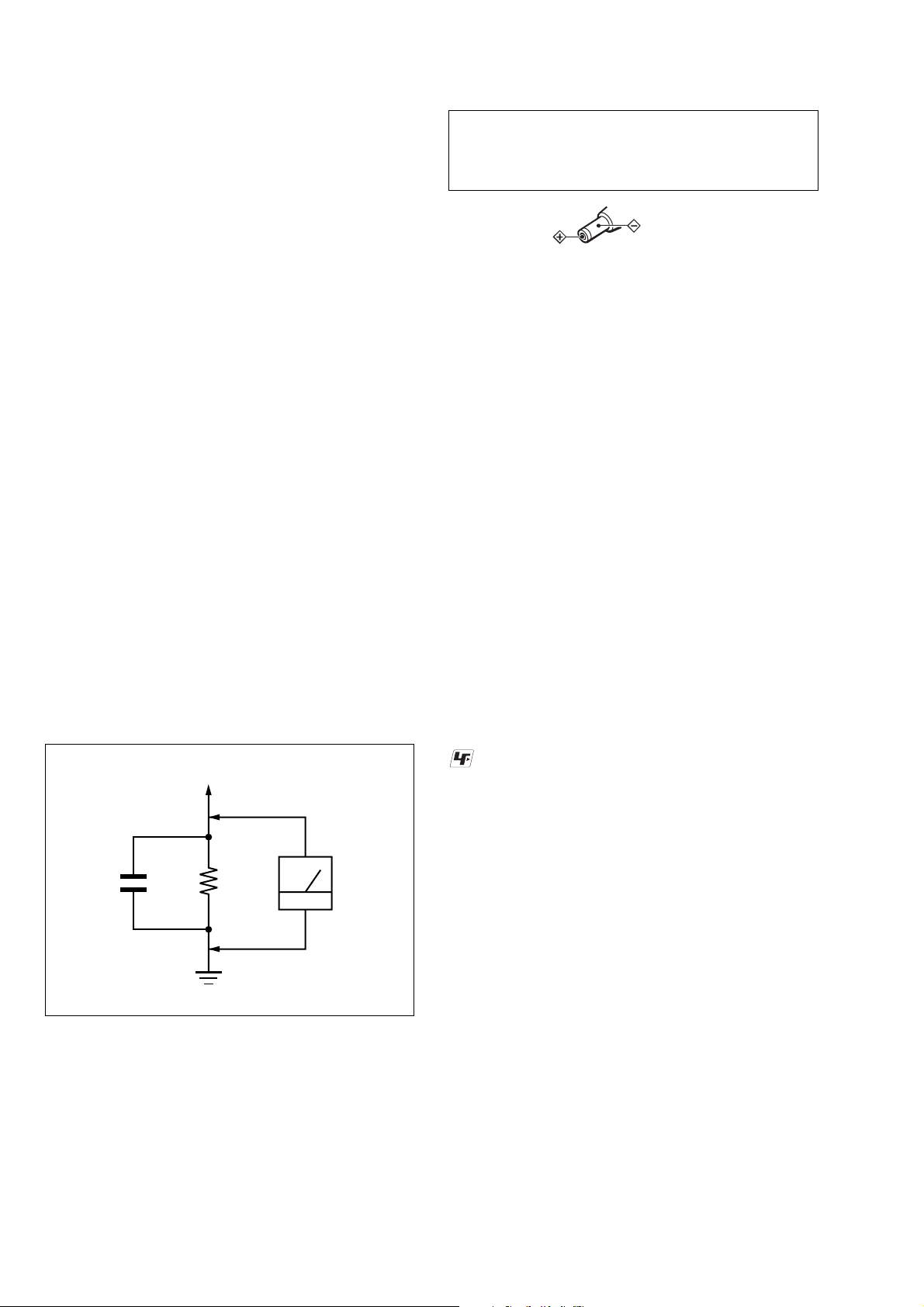
LEAKAGE TEST
The AC leakage from any exposed metal part to earth ground and
from all exposed metal parts to any exposed metal part having a
return to chassis, must not exceed 0.5 mA (500 microamperes).
Leakage current can be measured by any one of three methods.
1. A commercial leakage tester, such as the Simpson 229 or RCA
WT -540A. Follo w the manufacturers’ instructions to use these
instruments.
2. A battery-operated AC milliammeter. T he Data Precision 245
digital multimeter is suitable for this job.
3. Measuring the voltage drop across a resistor by means of a
VOM or battery-operated AC voltmeter. The “limit” indication is 0.75 V, so analog meters must have an accurate lowvoltage scale. The Simpson 250 and Sanwa SH-63T rd are examples of a passive VOM that is suitable. Nearly all battery
operated digital multimeters that have a 2 V A C range are suitable. (See Fig. A)
CAUTION
Use of controls or adjustments or performance of procedures
other than those specified herein may result in hazardous radiation exposure.
On power sources
•For AC operation,
use the supplied
AC power
adaptor; do not
use any other type.
• The player is not disconnected from the
AC power source (mains) as long as it is
connected to the wall outlet, even if the
player itself has been turned off.
• Unplug the player from the wall outlet
when it is not to be used for an extended
period of time.
•For battery operation, use six size D (R20)
batteries.
• When the batteries are not to be used,
remove them to avoid damage that can be
caused by battery leakage or corrosion.
• The nameplate indicating operating
voltage, etc. is located at the bottom.
About CD-Rs/CD-RWs
This player can play CD-Rs/CD-RWs
recorded in the CD-DA format*, but
playback capability may vary depending on
the quality of the disc and the condition of
the recording device.
* CD-DA is the abbreviation for Compact
Disc Digital Audio. It is a recording
standard used for Audio CDs.
Polarity of
the plug
UNLEADED SOLDER
Boards requiring use of unleaded solder are printed with the leadfree mark (LF) indicating the solder contains no lead.
(Caution: Some printed circuit boards may not come printed with
the lead free mark due to their particular size)
To Exposed Metal
Parts on Set
AC
1.5 k
0.15 µF
Fig. A. Using an AC voltmeter to check AC leakage.
SAFETY-RELATED COMPONENT WARNING!!
COMPONENTS IDENTIFIED BY MARK 0 OR DOTTED
LINE WITH MARK 0 ON THE SCHEMATIC DIAGRAMS
AND IN THE PARTS LIST ARE CRITICAL TO SAFE
OPERATION. REPLACE THESE COMPONENTS WITH
SONY PARTS WHOSE PART NUMBERS APPEAR AS
SHOWN IN THIS MANU AL OR IN SUPPLEMENTS PUBLISHED BY SONY.
Ω
Earth Ground
voltmeter
(0.75 V)
: LEAD FREE MARK
Unleaded solder has the following characteristics.
• Unleaded solder melts at a temperature about 40 ˚C higher than
ordinary solder.
Ordinary soldering irons can be used but the iron tip has to be
applied to the solder joint for a slightly longer time.
Soldering irons using a temperature regulator should be set to
about 350 ˚C.
Caution: The printed pattern (copper foil) may peel away if the
heated tip is applied for too long, so be careful!
• Strong viscosity
Unleaded solder is more viscou-s (sticky, less prone to flow)
than ordinary solder so use caution not to let solder bridges occur such as on IC pins, etc.
• Usable with ordinary solder
It is best to use only unleaded solder but unleaded solder may
also be added to ordinary solder.
ATTENTION AU COMPOSANT AYANT RAPPORT
À LA SÉCURITÉ!
LES COMPOSANTS IDENTIFIÉS P AR UNE MARQUE 0
SUR LES DIAGRAMMES SCHÉMATIQUES ET LA LISTE
DES PIÈCES SONT CRITIQUES POUR LA SÉCURITÉ
DE FONCTIONNEMENT. NE REMPLACER CES COMPOSANTS QUE PAR DES PIÈCES SONY DONT LES
NUMÉROS SONT DONNÉS DANS CE MANUEL OU
DANS LES SUPPLÉMENTS PUBLIÉS PAR SONY.
2

TABLE OF CONTENTS
ZS-X1
Ver 1.1
1. SERVICING NOTES.............................................. 4
2. GENERAL .................................................................. 5
3. DISASSEMBLY
3-1. Disassembly Flow ........................................................... 6
3-2. Cabinet Lower Assy, Telescopic Antenna (ANT1) ........ 7
3-3. Main Chassis Section ...................................................... 8
3-4. AUDIO Board, BATTERY Board .................................. 8
3-5. TUNER Board, CONTROL Board................................. 9
3-6. CD Mechanism Deck Section ......................................... 10
3-7. Optical Pick-up (KSS-213R) .......................................... 10
3-8. Cabinet Front Section ..................................................... 11
3-9. Speaker (10cm) (L) (SP101),
Speaker (10cm) (R) (SP201) .......................................... 11
3-10. Lid CD Assy .................................................................... 12
4. TEST MODE .............................................................. 13
5. ELECTRICAL ADJUSTMENTS
Tuner Section ................................................................. 14
CD Section ..................................................................... 15
6. DIAGRAMS
6-1. Block Diagram – CD Section – .................................... 16
6-2. Block Diagram – TUNER Section – ............................ 17
6-3. Block Diagram – MAIN Section – ............................... 18
6-4. Note for Printed Wiring Boards and
Schematic Diagrams ....................................................... 19
6-5. Printed Wiring Board – CD Section – .......................... 20
6-6. Schematic Diagram – CD Section – ............................. 21
6-7. Printed Wiring Board – TUNER Section
(US, CND, SP, KR, AUS models) – .............................. 22
6-8. Schematic Diagram – TUNER Section
(US, CND, SP, KR, AUS models) – .............................. 23
6-9. Printed Wiring Board
– TUNER Section (AEP, UK, IT, EE models) – ........... 24
6-10. Schematic Diagram
– TUNER Section (AEP, UK, IT, EE models) – ........... 25
6-11. Printed Wiring Boards
– AUDIO/PO WER Section – ......................................... 26
6-12. Schematic Diagram – A UDIO/POWER Section –....... 27
6-13. Printed Wiring Boards – CONTROL Section – ........... 28
6-14. Schematic Diagram – CONTROL Section –................ 29
6-15. Schematic Diagram – LCD/KEY Section –................. 30
6-16. IC Pin Function Description .......................................... 33
•Abbreviation
AUS: Australian model
CND : Canadian model
EE : East European model
IT : Italian model
KR : Korean model
SP : Singapore model
7. EXPLODED VIEWS
7-1. Cabinet Lower Section .................................................... 35
7-2. Cabinet Front Section ..................................................... 36
7-3. Cabinet Upper Section-1 ................................................. 37
7-4. Cabinet Upper Section-2 ................................................. 38
7-5. Cabinet Upper Section-3 ................................................. 39
7-6. Main Chassis Section ...................................................... 40
7-7. CD Block Section ........................................................... 41
7-8. Optical Pick-up Section (KSM-213RAP) ...................... 42
8. ELECTRICAL PARTS LIST .............................. 43
3
ZS-X1
SECTION 1
SERVICING NOTES
NOTES ON HANDLING THE OPTICAL PICK-UP
BLOCK OR BASE UNIT
The laser diode in the optical pick-up block may suffer electrostatic break-down because of the potential difference generated
by the charged electrostatic load, etc. on clothing and the human
body.
During repair, pay attention to electrostatic break-down and also
use the procedure in the printed matter which is included in the
repair parts.
The flexible board is easily damaged and should be handled with
care.
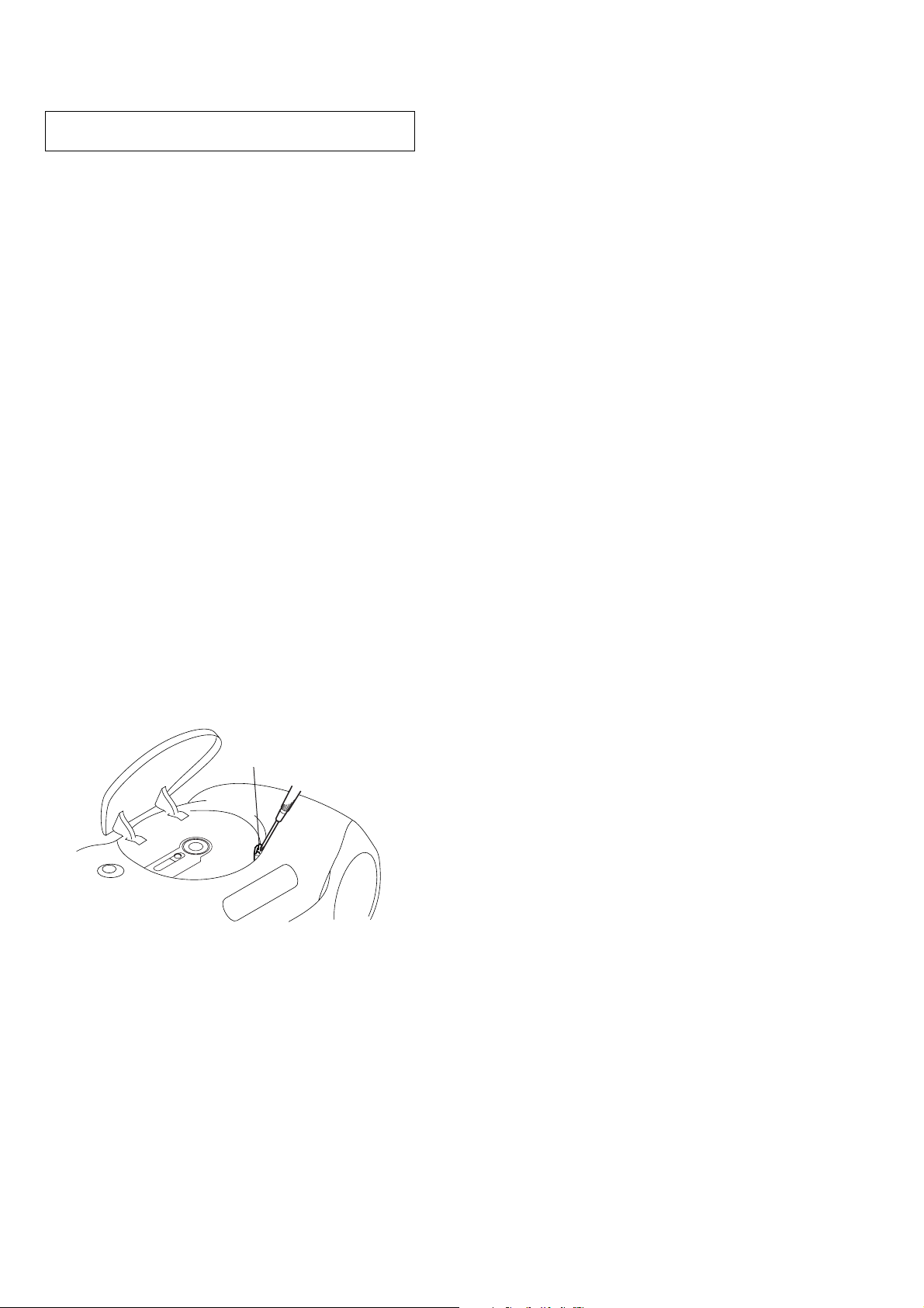
NOTES ON LASER DIODE EMISSION CHECK
The laser beam on this model is concentrated so as to be focused
on the disc reflective surface by the objective lens in the optical
pick-up block. Therefore, when checking the laser diode emission, observe from more than 30 cm away from the objectiv e lens.
LASER DIODE AND FOCUS SEARCH OPERATION
CHECK
During normal operation of the equipment, emission of the laser
diode is prohibited unless the upper lid is closed while turning ON
the S801. (push switch type)
The following checking method for the laser diode is operable.
• Method
Emission of the laser diode is visually checked.
1. Open the upper lid.
2. Push the S801 as shown in Fig.1.
Note: Do not push the detection lever strongly, or it may be bent or dam-
aged.
3. Check the object lens for confirming normal emission of the
laser diode. If not emitting, there is a trouble in the automatic
power control circuit or the optical pick-up.
In this operation, the object lens will move up and down 4
times along with inward motion for the focus search.
S801
Fig.1 Method to push the S801
4
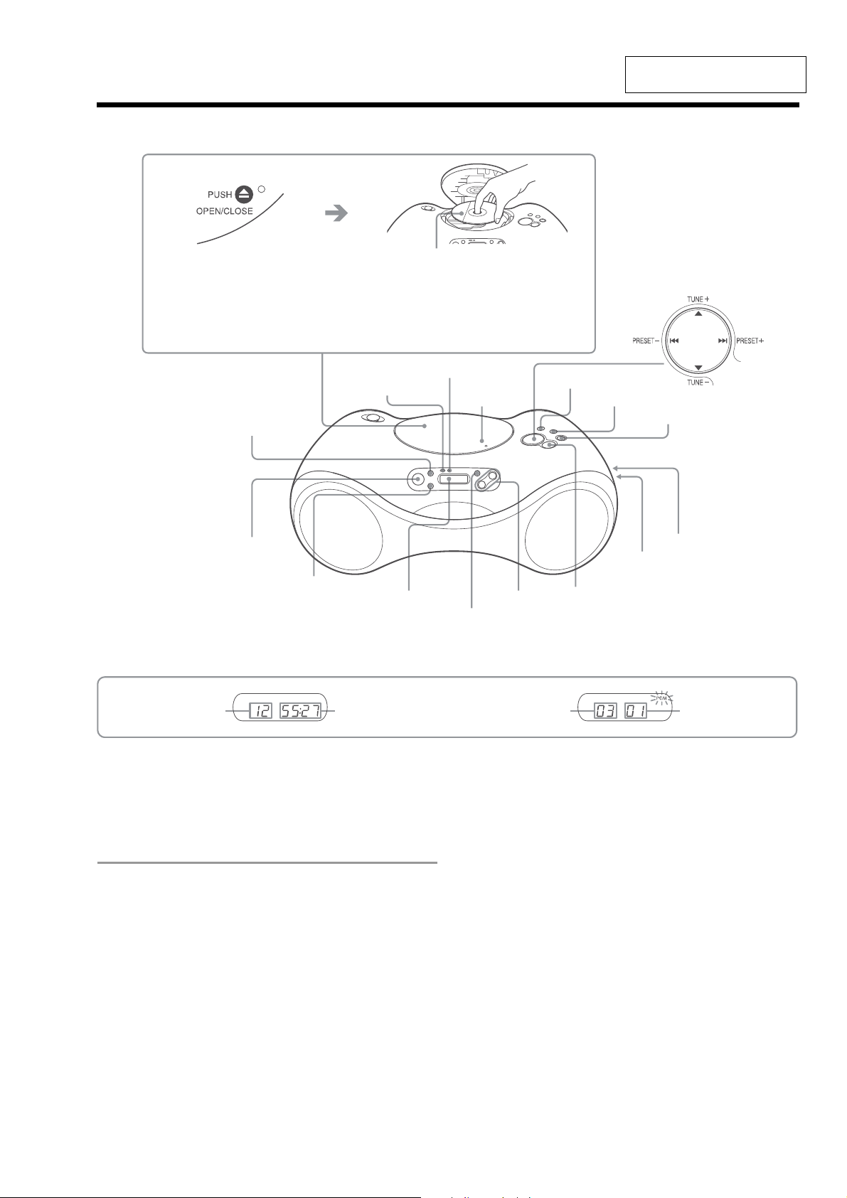
To turn on/off the power
European model: Press OPERATE.
Other models: Press POWER.
To adjust the volume
Press VOL +, –.
To listen through headphones
Connect the headphones to the i (headphones) jack.
Adjusting the sound emphasis
To reinforce the bass sound
Press MEGA BASS.
“MEGA BASS” appears in the display.
To return to normal sound, press the button again.
Location of controls
Total track number
Programmed track Playing order
CD
Total playing time
Display/Visor
MEGA BASS
VOL –, +*
DISPLAY/ENT
MEMORY
MODE
i
x
u*
POWER
(US, CND, SP, KR, AUS models)
OPERATE
(AEP, UK, IT, EE models)
DC IN 9V
OPR/BATT
Loading a CD
With the labeled side up
ESP
BAND
AUTO PRESET
ESP indicator
Indicador ESP
Display
Visor
*The button has a tactile dot.
Z PUSH
OPEN/CLOSE
Note
When inserting a CD, place the player horizontally.
If the player is not level, you cannot open or close the CD compartment lid.
SECTION 2
GENERAL
ZS-X1
Ver 1.1
This section is extracted from
instruction manual.
•Abbreviation
AUS: Australian model
CND : Canadian model
EE : East European model
IT : Italian model
KR : Korean model
SP : Singapore model
5
ZS-X1
• This set can be disassembled in the order shown below.
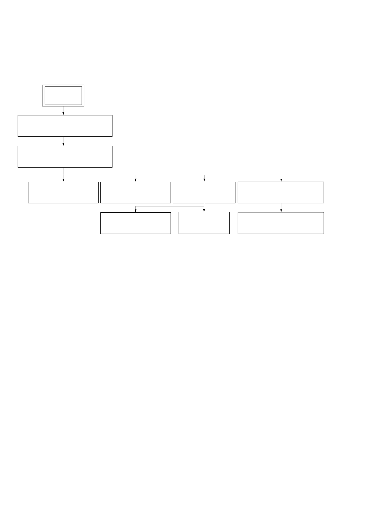
3-1. DISASSEMBLY FLOW
SET
3-2. CABINET LOWER ASSY,
TELESCOPIC ANTENNA (ANT1)
(Page 7)
3-3. MAIN CHASSIS SECTION
(Page 8)
SECTION 3
DISASSEMBLY
3-4. AUDIO BOARD,
BATTERY BOARD
(Page 8)
3-5. TUNER BOARD,
CONTROL BOARD
(Page 9)
3-7. OPTICAL PICK-UP
(KSS-213R)
(Page 10)
3-6. CD MECHANISM
DECK SECTION
(Page 10)
3-10.LID CD ASSY
(Page 12)
3-8. CABINET FRONT SECTION
(Page 11)
3-9. SPEAKER (10cm) (L) (SP101),
SPEAKER (10cm) (R) (SP201)
(Page 11)
6
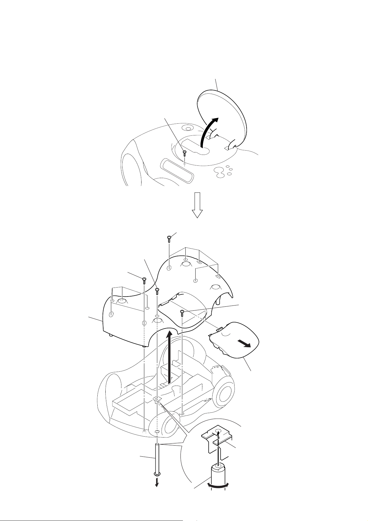
Note: Follow the disassembly procedure in the numerical order given.
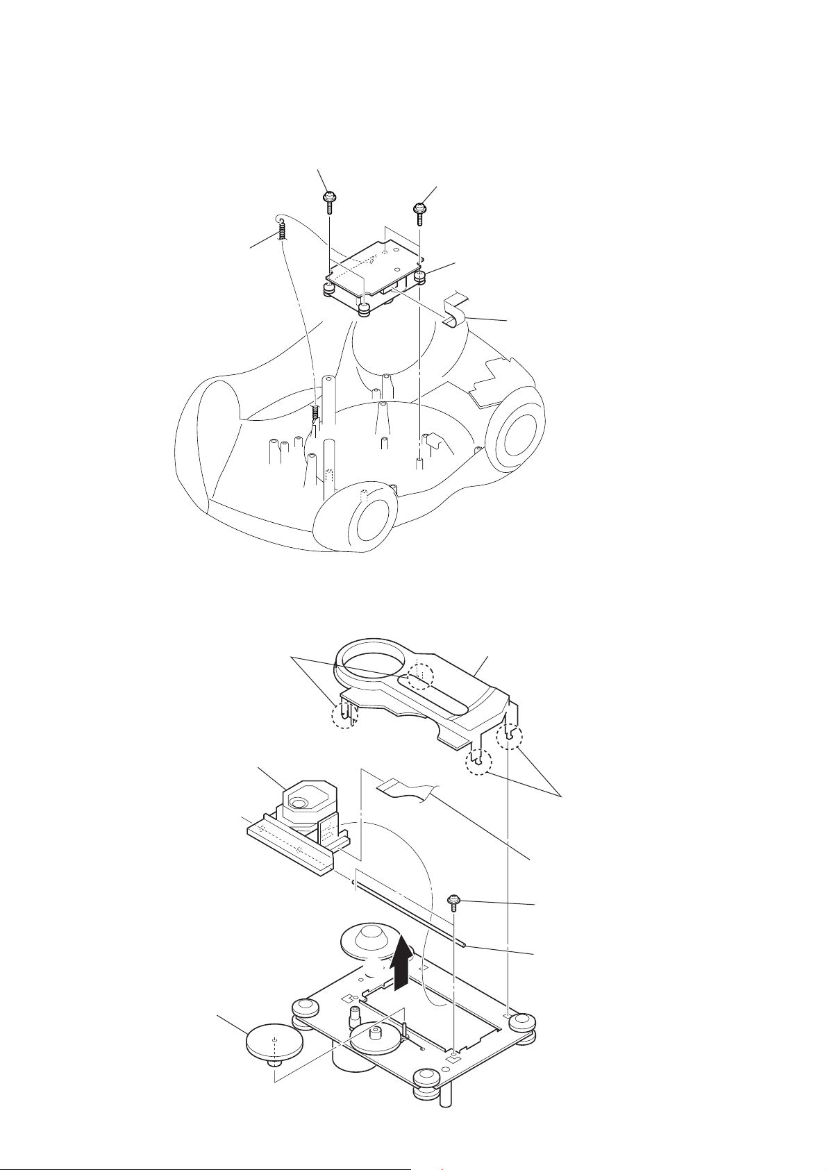
3-2. CABINET LOWER ASSY, TELESCOPIC ANTENNA (ANT1)
1
Open the CD lid.
2
screw
×
(BVTP3
14)
ZS-X1
6
cabinet lower
assy
4
five screws
(BVTP3
×
5
14)
screw
(B3
4
five screws
×
(BVTP3
×
8)
14)
4
two screws
(BVTP3
3
×
14)
battery case
lid
7
telescopic antenna
(ANT1)
!
telescopic antenna
(ANT1)
A
main chassis
Note: Install the telescopic antenna with engaging
!
the
check that the antenna is engaged and
does not move even trying to rotate it
in the direction of arrow
portion to the main chassis, then
A
.
7
ZS-X1
)
3-3. MAIN CHASSIS SECTION
3
four screws
(BVTP3
×
10)
7
main chassis section
1
connector (CN302)
4
2
connector (CN303)
5
wire (
(CN803)
flat type) (27 core)
6
wire (
flat type) (14 core)
(CN804)
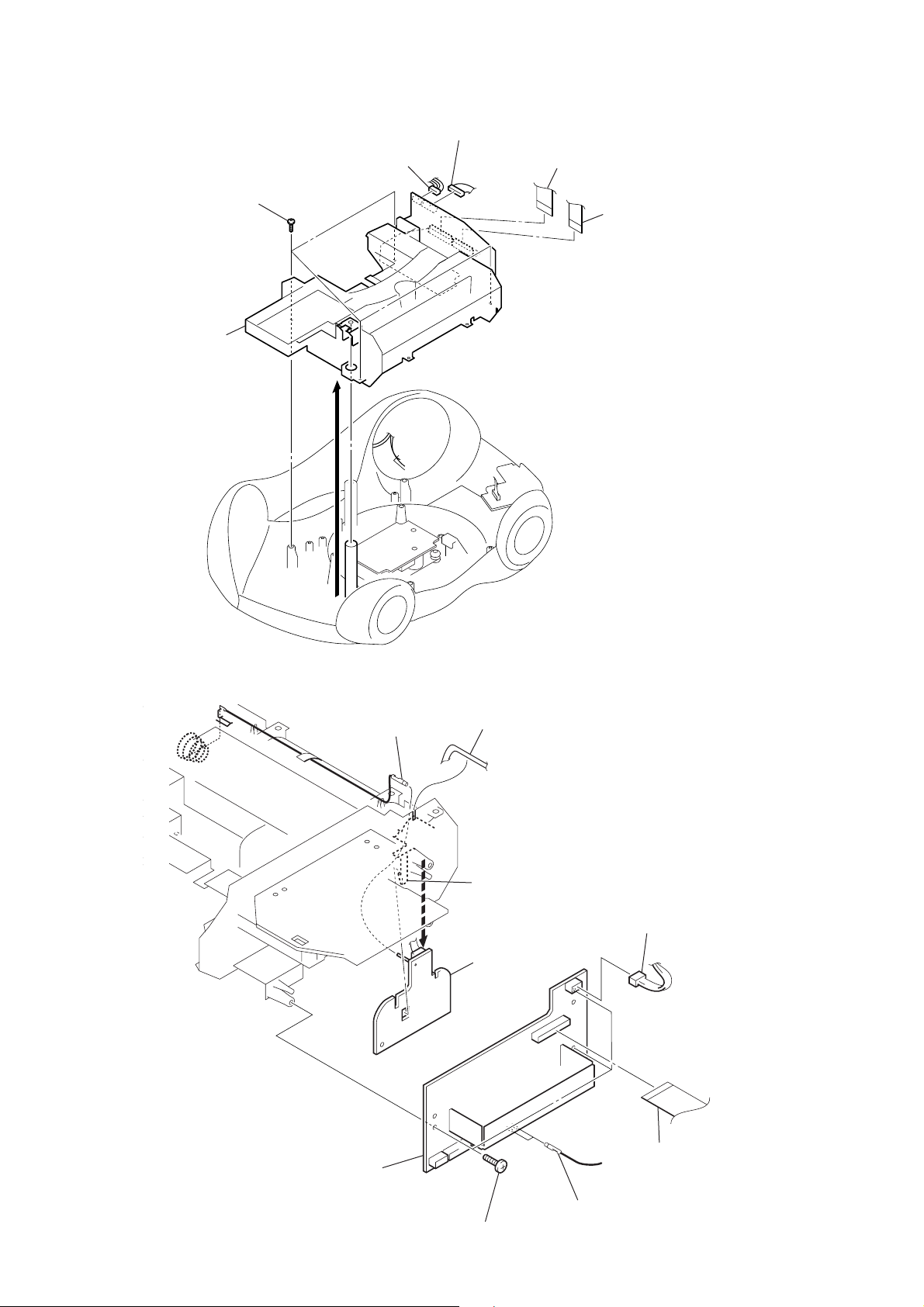
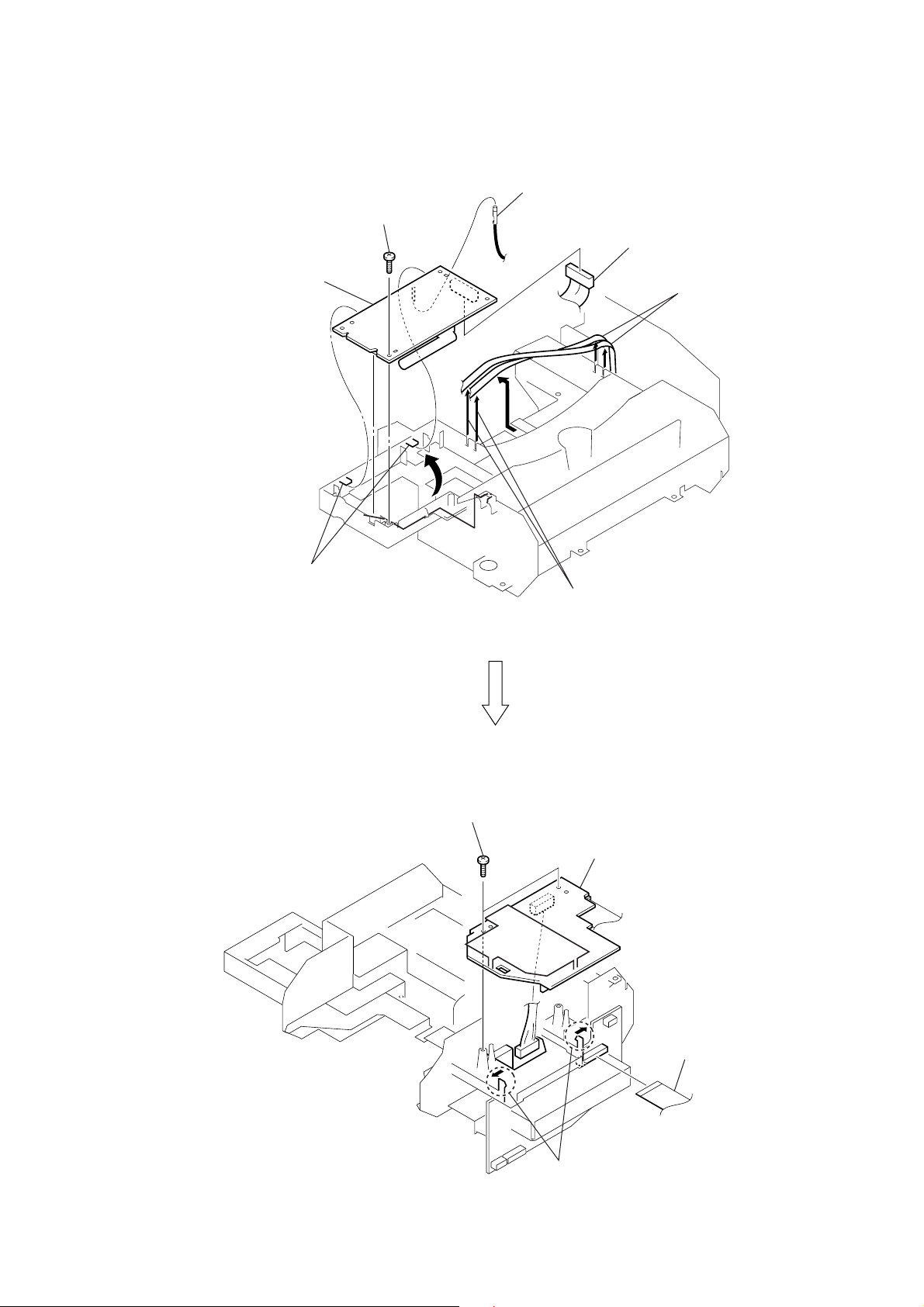
3-4. AUDIO BOARD, BATTERY BOARD
7
terminal
6
Remove the connector lead wire
from the incision.
8
claw
3
9
battery board
connector
(CN901)
1
wire (
flat type) (18 core
5
audio board
4
three screws
(BVTP3
×
10)
2
two terminals
(CN301)
8
3-5. TUNER BOARD, CONTROL BOARD
s
1
screw
(BVTP3
×
10)
6
tuner board
2
8
5
terminal
4
connector
(CNP1)
9
Remove the lead wire
from the incision.
ZS-X1
3
two convex portions
qa
two screws
(BVTP3
×
10)
7
Remove the connector lead wires
from the incision.
qd
control board
qs
two claws
0
wire (
(CN301)
flat type) (18 core)
9
ZS-X1
3-6. CD MECHANISM DECK SECTION
3
two
screws
(PWH2.6 × 10)
4
tension spring (CD)
2
two
screws
(PWH2.6 × 10)
5
CD mechanism deck section
1
flexible flat cable (14P)
(CN702)
3-7. OPTICAL PICK-UP
(KSS-213R)
1
two claws
9
optical pick-up (KSS-213R)
6
3
CD cover
2
two claws
7
flexible flat cable
5
two screws
(M2)
8
sled shaft
10
4
gear (A)
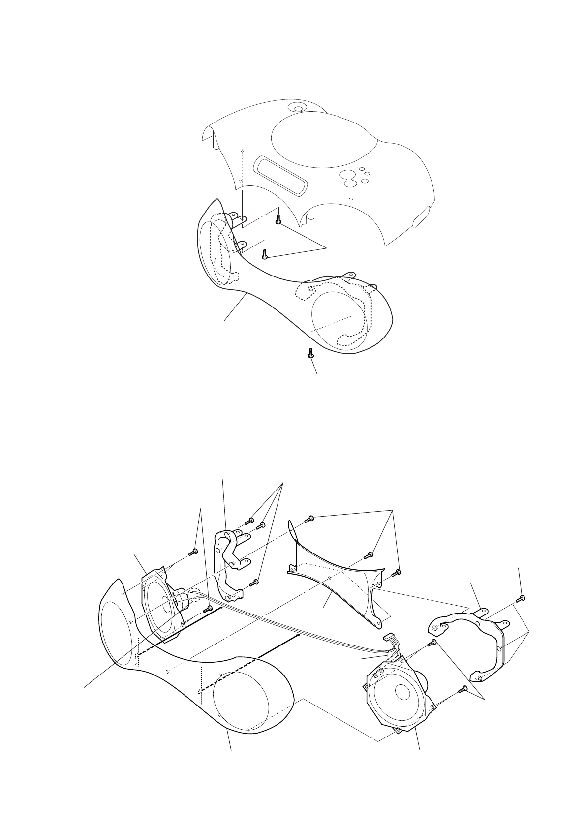
3-8. CABINET FRONT SECTION
1
two screws
(BVTP3
×
ZS-X1
10)
2
cabinet front section
1
two screws
×
(BVTP3
10)
3-9. SPEAKER (10cm) (L) (SP101), SPEAKER (10cm) (R) (SP201)
8
three screws
×
(BVTP3
10)
qs
speaker (10cm) (L)
(SP101)
qa
four screws
(BVTP3
9
holder front (L)
×
10)
1
five screws
(BVTP3
×
10)
4
holder front (R)
3
three screws
(BVTP3
×
10)
0
Remove two solders.
5
Remove two solders.
qd
cabinet front sub assy
2
handle cover
6
four screws
(BVTP3
7
speaker (10cm) (R) (SP201)
×
10)
11
ZS-X1
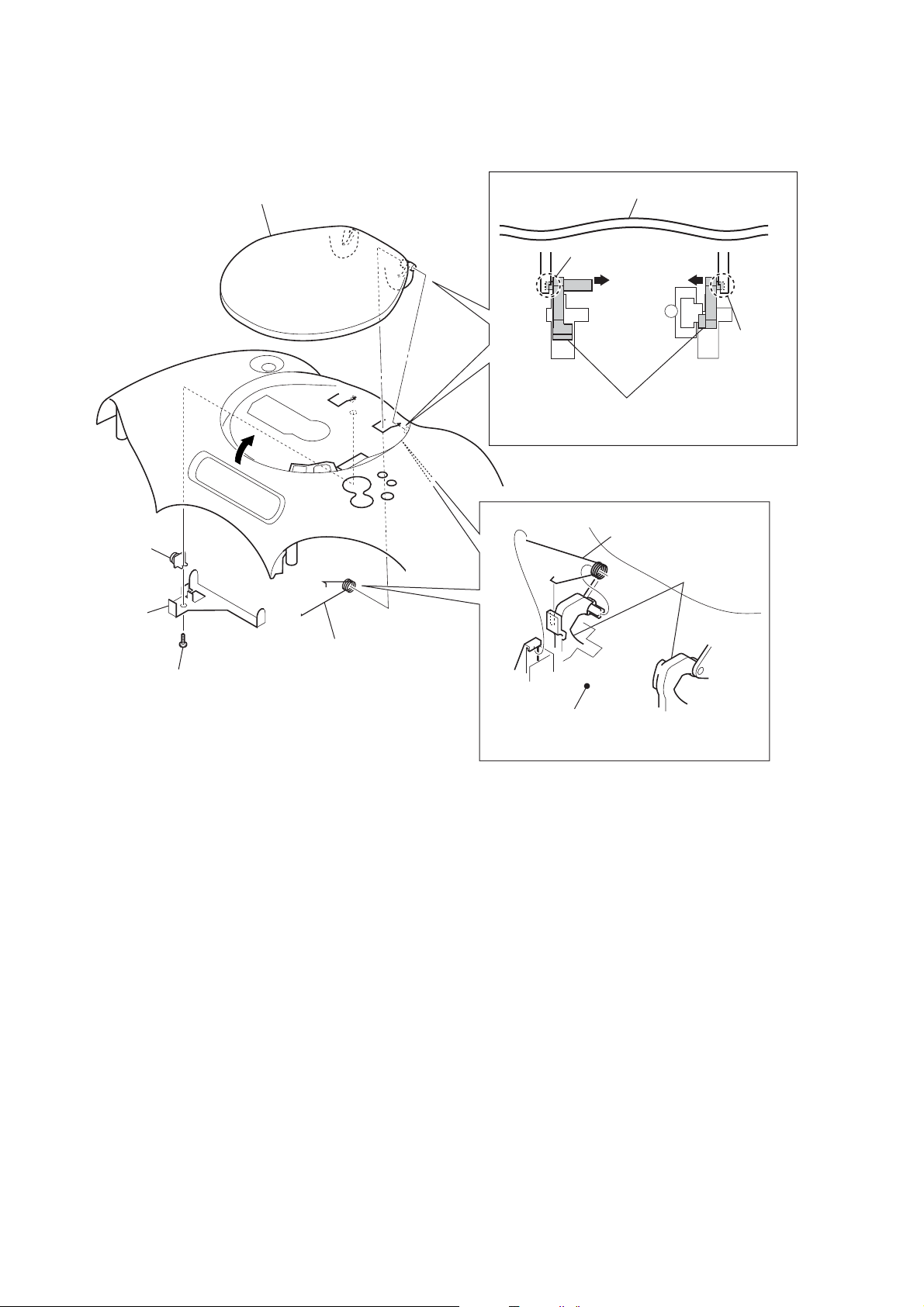
3-10. LID CD ASSY
3
2
plate (SE)
damper
8
lid
CD assy
7
cabinet upper
5
boss
lid
CD assy
– bottom view –
CD spring
lid
CD assy
6
boss
1
screw (BVTP3 × 10)
4
CD spring
cabinet upper
– bottom view –
12
SECTION 4
TEST MODE
CD TEST MODE
procedure:
1. Insert the disc (YEDS-18) (Part No. 3-702-101-01) (CD) or
(TCD-W082L) (Part No. J-2502-063-2) (CD-RW).
2. Press the [POWER] or [OPERATE] button to turn the power
on. (TOC read ended)
3. Set the test mode by momentarily shorting both of T AP (TEST-
A) on the LCD board. (The message “88” is displayed on the
liquid crystal display)
4. T o release the test mode, press the [POWER] or [OPERATE]
button to turn the power off.
LCD TEST MODE
procedure:
1. Press the [POWER] or [OPERATE] button to turn the power
on.
2. Set the test mode by momentarily shorting both of T AP (TEST-
B) on the LCD board.
LCD DISPLAY
1 All lighting (4 seconds)
t
r
2 COM0 lighting (2 seconds)
r
3 COM1 lighting (2 seconds)
r
4 COM2 lighting (2 seconds)
r
5 COM3 lighting (2 seconds)
ZS-X1
Ver 1.1
3. It repeats until any button is pressed.
Connecting Location:
– LCD BOARD (Conductor Side) –
TEST B
TEST A
13
ZS-X1
r
Ver 1.1
SECTION 5
ELECTRICAL ADJUSTMENTS
PRECAUTION
1. Setting
MEGA BASS : OFF
TUNER SECTION 0 dB=1 µV
[AM (MW/LW) ]
Setting:
Function: RADIO
Band: AM (US, CND, SP, KR, AUS)
MW or LW (AEP, UK, IT, EE)
AUDIO board
AM RF signal
generator
30% amplitude
modulation by
400 Hz signal
Output level:
as low as possible
Put the lead-wire
antenna close to
the set.
set
[FM]
Setting:
Function: RADIO
Band: FM
FM RF signal
generator
0.01 µF
75 kHz frequency
deviation by 1 kHz
signal
Output level:
as low as possible
TUNER board
TP (GND)
TUNER board
TP (ANT)
TUNER board
TP (GND)
TP (VT)
set
100 kΩ
•Repeat the procedures in each adjustment several times, and the
tracking adjustments should be finally done by the trimmer capacitors.
• Remove FM antenna in FM adjustment.
CN302 pin 1
level meter
3.2 Ω
+
–
AUDIO board
CN302 pin 2
AUDIO board
CN302 pin 1
level meter
3.2 Ω
+
–
AUDIO board
CN302 pin 2
digital voltmete
AM (MW/LW) IF ADJUSTMENT
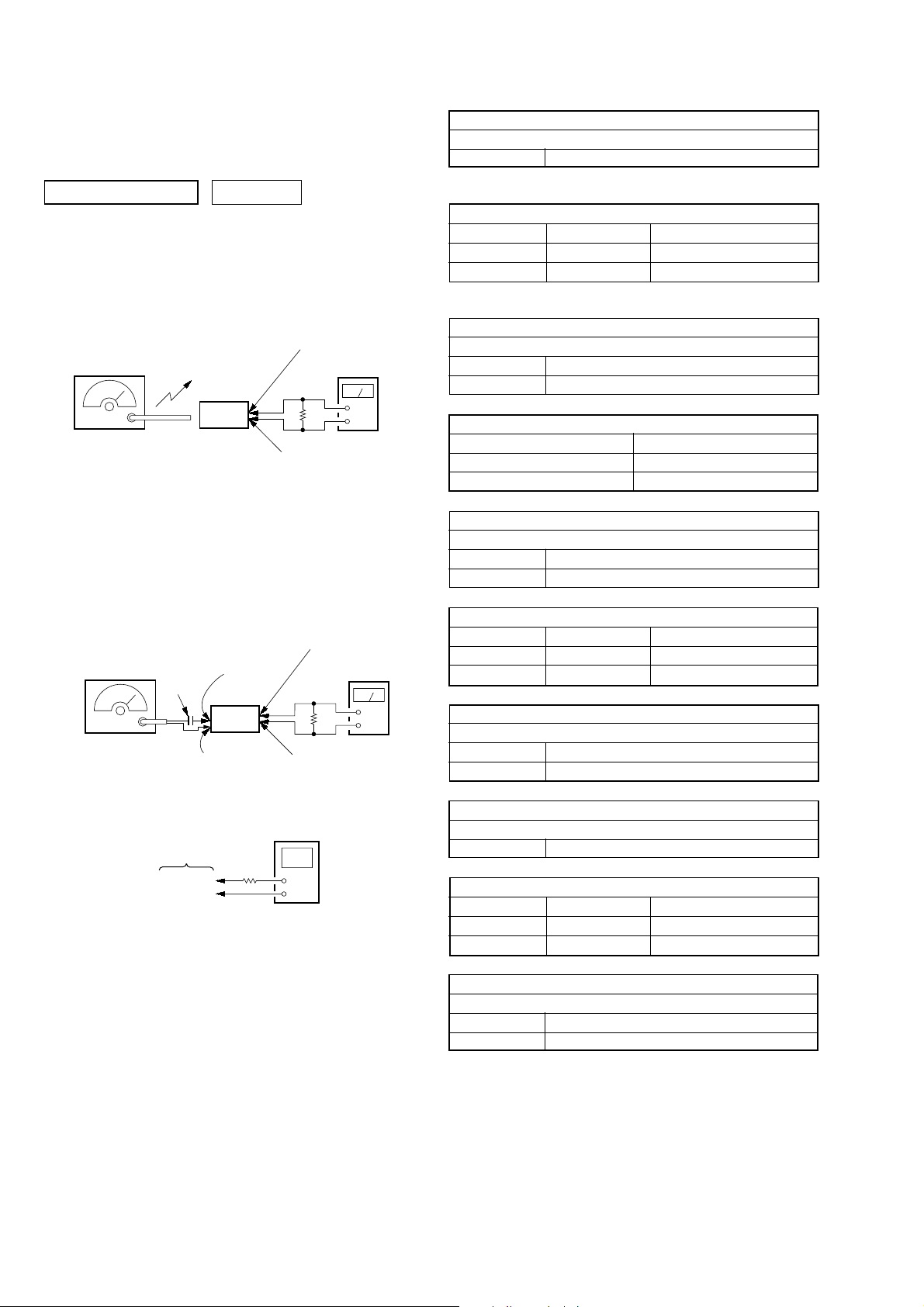
Adjust for a maximum reading on level meter
T1 450 kHz
(): Singapore, Korean, Australian models
AM VCO VOLTAGE ADJUSTMENT (US, CND, SP, KR, AUS)
Adjustment Part Frequency Display Reading on Digital Voltmeter
L4 530 (531) kHz 1.0 ± 0.05 V
Confirmation 1,710 (1,611) kHz 5.3 (4.8) ± 0.7 V
(): Singapore, Korean, Australian models
AM TRACKING ADJUSTMENT (US, CND)
Adjust for a maximum reading on level meter
L3 620 (621) kHz
CT3 1,400 (1,404) kHz
MW VCO VOLTAGE ADJUSTMENT (AEP, UK, IT, EE)
Frequency Display Reading on Digital Voltmeter
531 kHz 0.9 ± 0.4 V
1,611 kHz 5.2 ± 0.5 V
MW TRACKING ADJUSTMENT (AEP, UK, IT, EE)
Adjust for a maximum reading on level meter
L3-1 621 kHz
CT3 1,404 kHz
LW VCO VOLTAGE ADJUSTMENT (AEP, UK, IT, EE)
Adjustment Part Frequency Display Reading on Digital Voltmeter
L4 153 kHz 0.6 ± 0.2 V
Confirmation 279 kHz 5.0 ± 0.1 V
LW TRACKING ADJUSTMENT (AEP, UK, IT, EE)
Adjust for a maximum reading on level meter
L3-2 162 kHz
CT5 261 kHz
FM IF ADJUSTMENT
Adjust for a minimum reading on level meter
T2 10.7 MHz
FM VCO VOLTAGE ADJUSTMENT
Adjustment Part Frequency Display Reading on Digital Voltmeter
L2 108 MHz 3.0 ± 0.2 V
Confirmation 87.5 MHz 1.3 ± 0.3 V
FM TRACKING ADJUSTMENT
Adjust for a maximum reading on level meter
L1 87.5 MHz
CT1 108 MHz
14
Adjustment and Connecting Location: TUNER board
(See page 15)
ZS-X1
B
t
t
Ver 1.1
Adjustment and Connecting Location:
– TUNER BOARD (Component Side) (US, CND, SP, KR, AUS) –
AM VCO Voltage Adjustment
FM VCO Voltage Adjustment
AM T rac king Adjustment
L4
L2
CT3
L3
– TUNER BOARD (Component Side) (AEP, UK, IT, EE) –
LW VCO Voltage Adjustment
L4
T2 FM IF Adjustment
T1 AM IF Adjustment
L1
FM T rac king Adjustmen
CT1
T2 FM IF Adjustment
CD SECTION
Perform all CD section check in the test mode.
TRAVERSE CHECK
procedure:
1. Connect an oscilloscope to TP (TE) and TP (VC) on the CD
board.
2. Set the CD test mode. (Refer to CD TEST MODE (See page
13))
3. Press the u button once. (LCD DISPLAY “F –”)
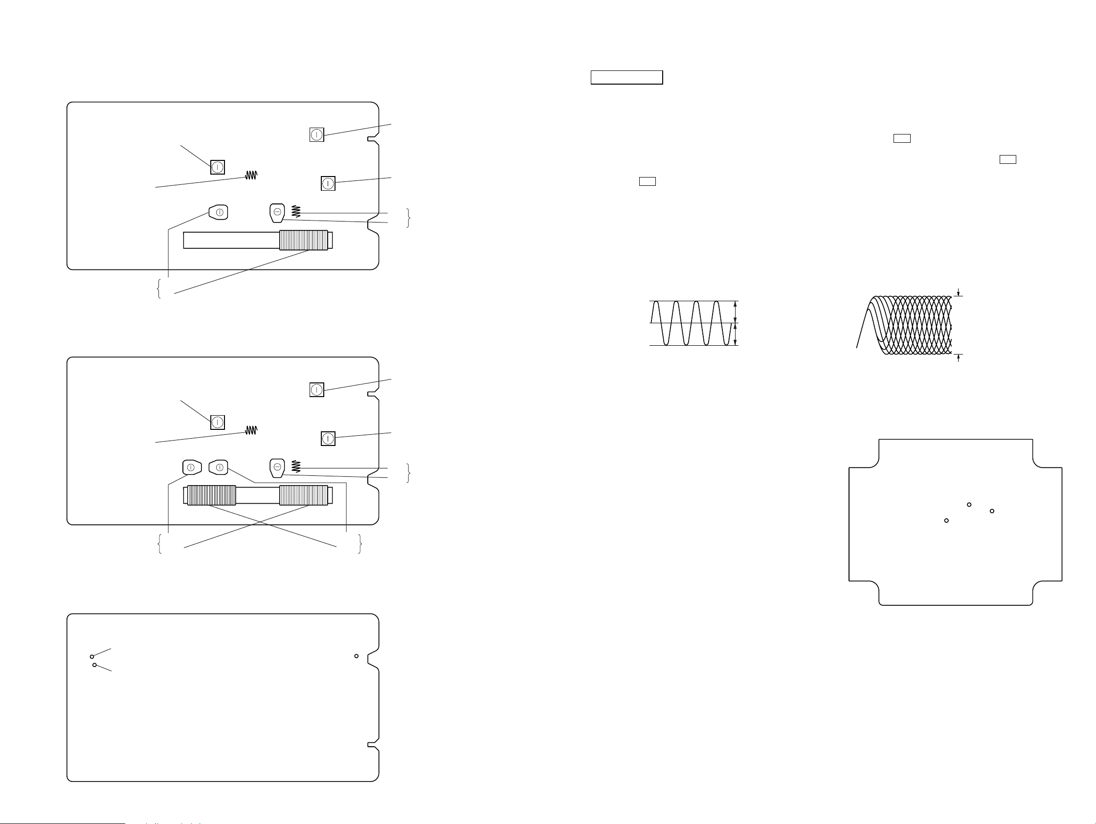
4. Confirm that the center of the oscilloscope wav eform is at 0 V.
5. Confirm that the oscilloscope wav eform Vp-p value is at 0.95
± 0.4 V.
6. To check CD-RW, turn the power off. Change discs to CDRW (TCD-W082L) (Part No. J-2502-063-2), then set the CD
test mode again. (Refer to CD TEST MODE (See page 13))
VOLT/DIV: 0.2 V (with the 10:1 probe in use)
TIME/DIV: 1 ms
A
0 V
Vp-p=A+
B
FOCUS BIAS CHECK
procedure:
1. Connect the oscilloscope to TP (RF) and TP (VC) on the CD
board.
2. Set the CD test mode. (Refer to CD TEST MODE (See page
13))
3. Press the u button twice. (LCD DISPLAY “P –”)
Note: If this check is performed continuously after the
TRAVERSE CHECK, press the u button once.
4. Confirm that the oscilloscope waveform is as shown in the
figure below. (eye pattern)
A good eye pattern means that the diamond shape (◊) in the
center of the waveform can be clearly distinguished.
5. To check CD-RW, turn the power off. Change discs to CDRW (TCD-W082L) (Part No. J-2502-063-2), then set the CD
test mode again. (Refer to CD TEST MODE (See page 13))
• RF signal reference waveform (eye pattern)
VOLT/DIV: 0.2 V (with the 10: 1 probe in use.)
TIME/DIV: 500 ns
CD:
±
0.3 Vp-p
1.0
CD-RW:
1.0
±
0.4 Vp-p
When observing the eye pattern, set the oscilloscope
for AC range and raise vertical sensitivity.
Connecting Location:
FM VCO Voltage Adjustment
LW Tracking Adjustment
L2
CT3
L3-2
– TUNER BOARD (Conductor Side) –
TP
(VT)
TP
(GND)
T1 AM IF Adjustment
L1
CT1
CT3
MW T rac king Adjustment
L3-1
TP
(ANT)
FM T rac king Adjustmen
– CD BOARD (Conductor Side) –
TP
(TE)
TP
(RF)
TP
(VC)
•Abbreviation
AUS: Australian model
CND : Canadian model
EE : East European model
IT : Italian model
KR : Korean model
SP : Singapore model
1515
ZS-X1
SECTION 6
DIAGRAMS
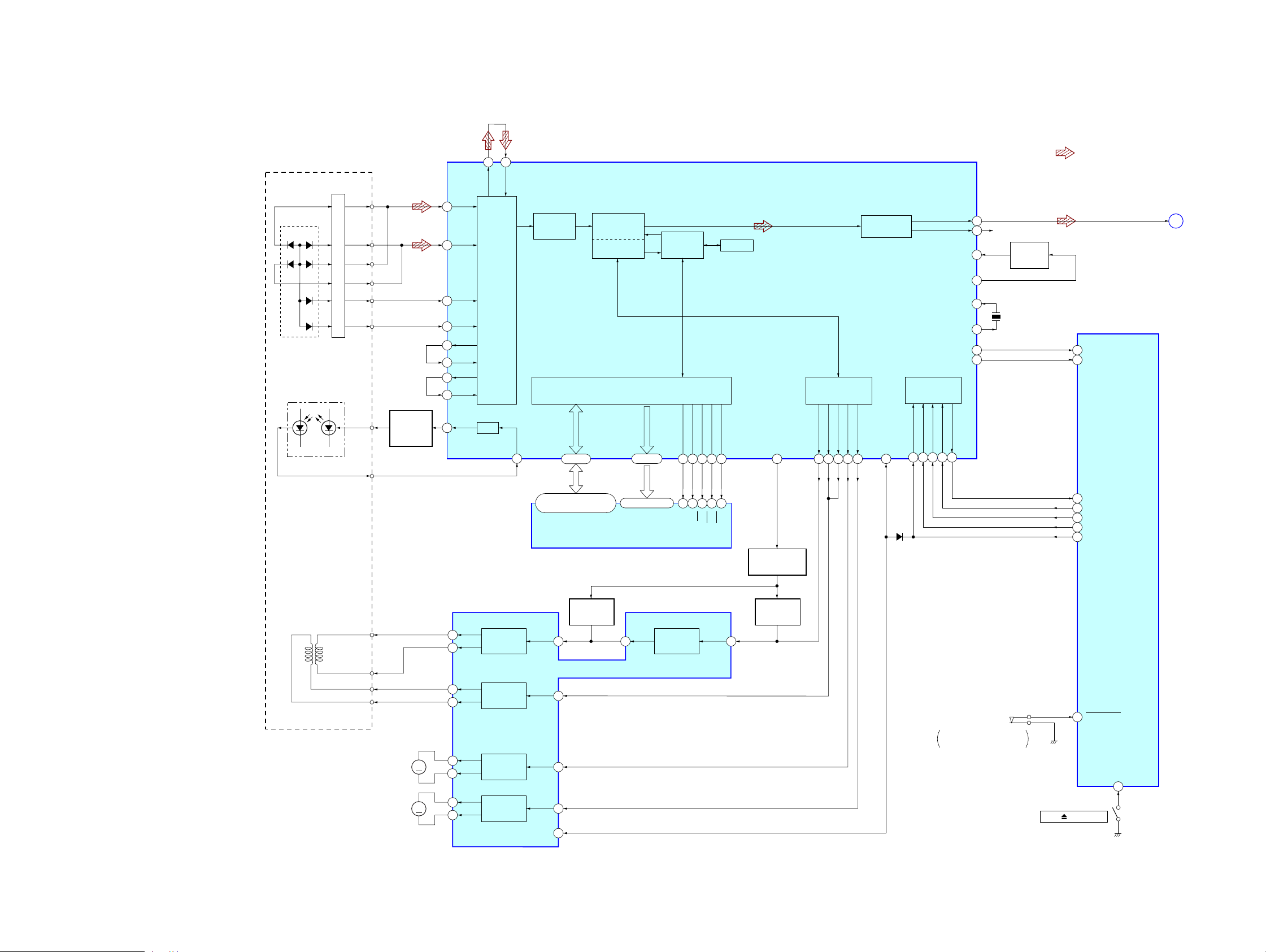
6-1. BLOCK DIAGRAM – CD Section –
2
3
6
5
9
8
96
97
AC (I)
BD (I)
F (I)
E (I)
FEO (O)
FEN (I)
TEO (O)
TEN (I)
DETECTOR
A
D
C
B
F
E
OPTICAL PICK-UP
BLOCK
(KSM-213RAP)
LASER DIODE
I-V AMP
A
D
C
B
F
E
99
100
RFI (I)
EQO (O)
RF SIGNAL
GENERATOR
SERVO
SIGNAL
GENERATOR
DIGITAL SERVO SIGNAL PROCESSOR,
X8 OVER
SAMPLIMG
DIGITAL FILTER
DIGITAL SERVO
FILTER
ANTI-SHOCK
MEMORY CONTROLLER
RF AMP, FOCUS/TRACKING SERVO,
DIGITAL SIGNAL PROCESSOR,
DIGITAL FILTER, D/A CONVERTER,
ANTI-SHOCK MEMORY CONTROLLER
DIGITAL
SIGNAL
PROCESSOR
IC701
16K SRAM
DIGITAL SERVO
SIGNAL PROCESSOR
1BIT
D/A CONVERTER
COMMAND
INTERFACE
LDACO
RDACO
MONI0
MONI1
XI (I)
XO (O)
BUSY
SUBSYQ
• R-ch is omitted due to same as L-ch.
• SIGNAL PATH
: CD PLAY
80
R-CH
82
89
90
76
77
35
29
ERROR
MONITOR
Q702
X701
16.9344MHz
61 C-BUSY (I)
52 C-SUBSYQ (I)
CD-LOUT
A
(Page 18)
PD
2-AXIS
DEVICE
(TRACKING)
LD
(FOCUS)
LD
PD
AUTOMATIC
POWER
CONTROL
Q701
F+
F–
T+
T–
M702
M
(SLED)
M701
M
(SPINDLE)
LD (O)
13
APC
FOCUS/TRACKING COIL DRIVE,
SPINDLE/SLED MOTOR DRIVE
F+
17
F–
18
T+
12
T–
11
SL+
27
SL–
26
SP+
2
SP–
1
IC703
FOCUS
COIL DRIVE
TRACKING
COIL DRIVE
SLED
MOTOR DRIVE
SPINDLE
MOTOR DRIVE
PD (I)
12
2, 3, 5, 6, 8, 9, 11, 12, 39,
40, 42, 43, 45, 46, 48, 49
(FIN)
TIN
(SLIN)
SPIN
DQ00 – DQ15
56 – 71 41 – 52
19 – 24, 27 – 32
DQ0 – DQ15
16M BIT SD-RAM
IC702
FOCUS GAIN
UP SWITCH
Q705
20
9
24
3
7MUTE
14
A00 (O) – A11 (O)
A0 – A11
OPOUT
FOCUS
COIL DRIVE
RCLK (O)
RCKE (O)
WEX (O)
CASX (O)
37 38 55 54 53
35
34
15
16
WE
CLK
CKE
CAS
OPIN
RASX (O)
17
RAS
15
XPLCK
91
FOCUS GAIN
CONTROL SWITCH
Q703
FOCUS GAIN
UP SWITCH
Q704
TDOUT (O)20JUMPO (O)23SDOUT (O)24CLVOUT (O)
FDOUT (O)
21
19
DFDIN (I)
88
D703
34
RESETX33RW (I)30MCK (I)31DIN (I)32DOUT (O)
When the optical pick-up
ON :
is inner position
S701
(LIMIT)
53 C-DOUT (I)
54 C-DIN (O)
55 C-MCK (O)
62 C-RW (O)
64 C-RESETX (O)
63 C-LIM SW (I)
S801
PUSH OPEN/CLOSE
SYSTEM
CONTROLLER
IC802 (1/2)
C-DOOR
29
1616
 Loading...