

Sony XM-1902-SX Service manual

XM-1502SX/1902GX
SERVICE MANUAL
Ver 1.3 2002. 07
Photo: XM-1902GX
SPECIFICATIONS
AUDIO POWER SPECIFICA TIONS
POWER OUTPUT AND TOTAL HARMONIC DISTORTION
150 watts per channel minimum continuous average power into
4 ohms, both channels driven from 20 Hz to 20 kHz with no more
than 0.04% total harmonic distortion per Car Audio Ad Hoc
Committee standards.
US Model
XM-1502SX/1902GX
Canadian Model
AEP Model
UK Model
E Model
XM-1502SX
Other Specifications
Circuit system OTL (output transformerless) circuit
Inputs RCA pin jacks
Outputs Speaker terminals
Speaker impedance 2 – 8 Ω (stereo) (XM-1502SX)
Maximum outputs 300 W × 2 (at 4 Ω)
Rated outputs (supply voltage at 14.4 V)
Frequency response 5 Hz – 100 kHz ( dB)
Harmonic distortion 0.005% or less (at 1 kHz, 4 Ω)
Input level adjustment range
Pulse power supply
High level input connector
Through out pin jacks
1.3 – 8 Ω (stereo) (XM-1902GX)
4 – 8 Ω (when used as a bridging amplifier)
760 W (monaural) at 4 Ω
150 W × 2 (20 Hz – 20 kHz, 0.04% THD,
at 4 Ω)
190 W × 2 (20 Hz – 20 kHz, 0.1% THD,
at 2 Ω)
190 W × 2 (20 Hz – 20 kHz, 0.1% THD,
at 1.3 Ω) (XM-1902GX)
380 W × 1 (20 Hz – 20 kHz, 0.1% THD,
at 4 Ω) (XM-1902GX)
380 W (monaural) (20 Hz – 20 kHz, 0.1% THD,
at 4 Ω) (XM-1502SX)
0.2 – 6.0 V (RCA pin jacks)
0.4 – 12.0 V (High level input)
+0.5
–3
High-pass filter 50 – 300 Hz, –12 dB/oct
Low-pass filter 50 – 300 Hz, –12 dB/oct
Low boost 0 – 10 dB (40 Hz)
Phase shift adjustment range (XM-1902GX)
Power supply voltage 10.5 – 16 V
Current drain at rated output : 40 A (at 4 Ω)
Dimensions Approx. 358 × 50 × 264 mm
Mass Approx. 3.5 kg (7 lb. 11 oz.) not incl. accessories
Supplied accessories Mounting screws (4)
Design and specifications are subject to change without
notice.
0° – 180° (at 40 Hz)
Remote input : 2 mA
1/8 × 2 1/4 × 10 1/2 in.)
(14
(w/h/d) not incl. projecting parts and controls
9-870-239-14
2002G0400-1
© 2002. 07
STEREO POWER AMPLIFIER
Sony Corporation
e Vehicle Company
Published by Sony Engineering Corporation
1

TABLE OF CONTENTS
1. GENERAL
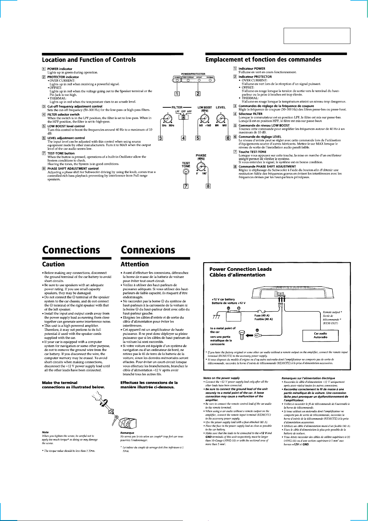
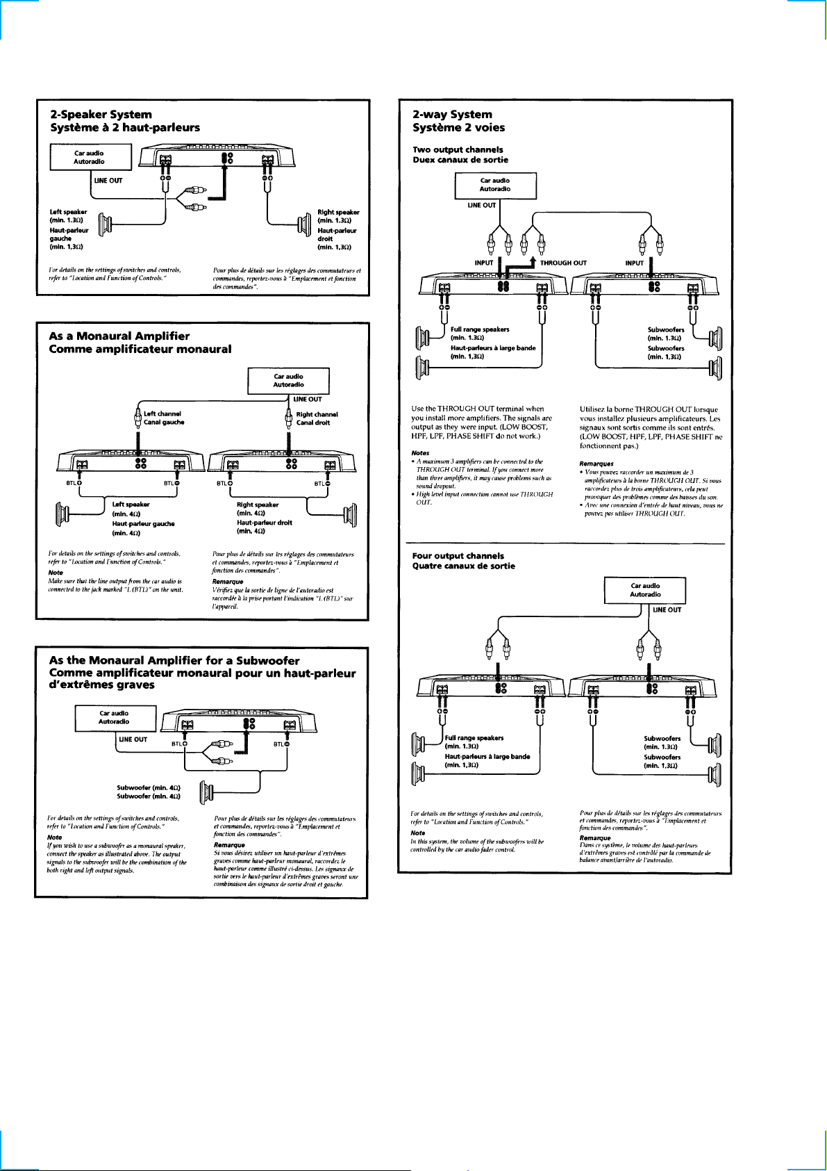
Location and Function of Controls.......................................... 3
Connections ............................................................................. 3
2. DISASSEMBLY
2-1. Plate, Bottom....................................................................... 6
2-2. Main Board ......................................................................... 6
2-3. Front Panel .......................................................................... 7
2-4. Led Board ............................................................................ 7
3. ELECTRICAL ADJUSTMENT...................................... 8
4. DIAGRAMS
4-1. Block Diagram .................................................................... 9
4-2. Printed Wiring Boards –Main Section– ............................ 11
4-3. Schematic Diagram –Main Section (1/2)– ........................ 12
4-4. Schematic Diagram –Main Section (2/2)– ........................ 13
5. EXPLODED VIEWS
5-1. Heat Sink Section .............................................................. 14
5-2. Main Board Section .......................................................... 14
6. ELECTRICAL PARTS LIST......................................... 15
Notes on Chip Component Replacement
• Never reuse a disconnected chip component.
• Notice that the minus side of a tantalum capacitor may be dam-
aged by heat.
2
SECTION 1
GENERAL
This section is extracted
from instruction manual.
3
456

SECTION 2
DISASSEMBLY
Note : Follow the disassembly procedure in the numerical order given.
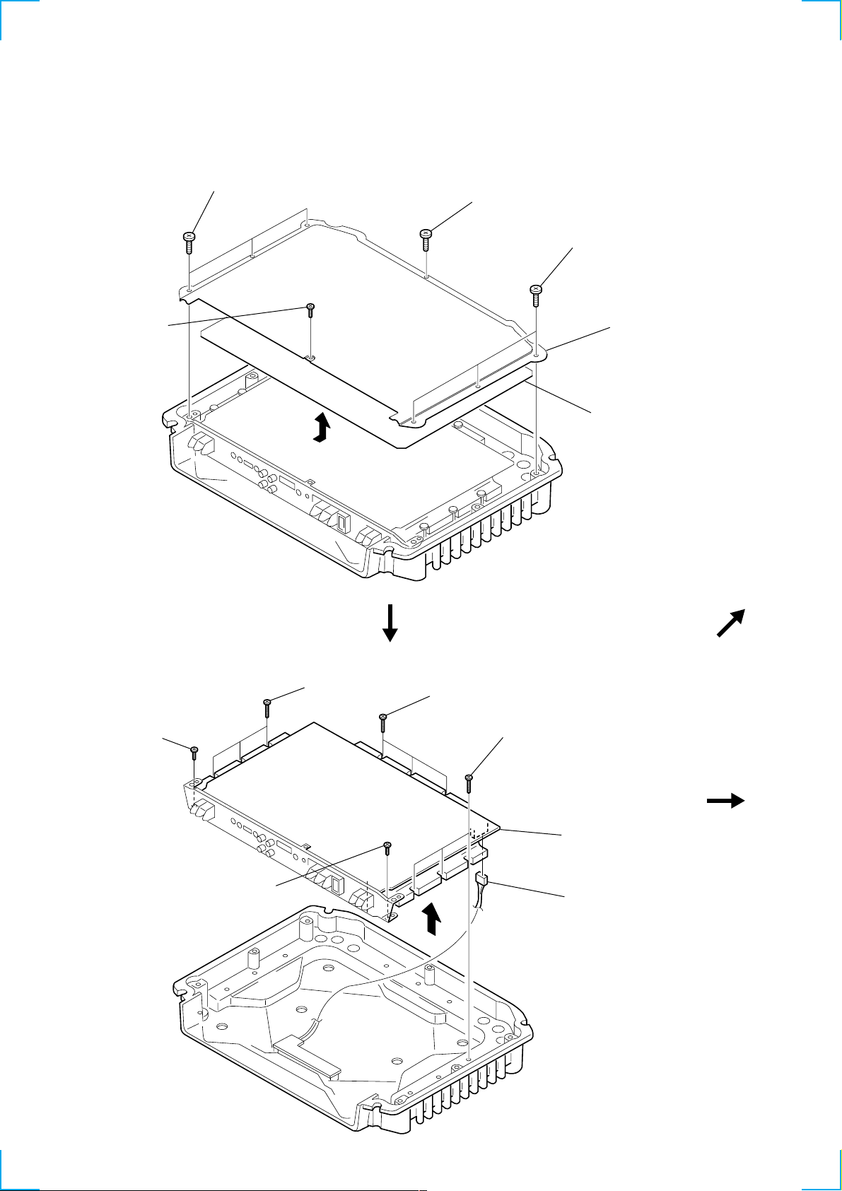
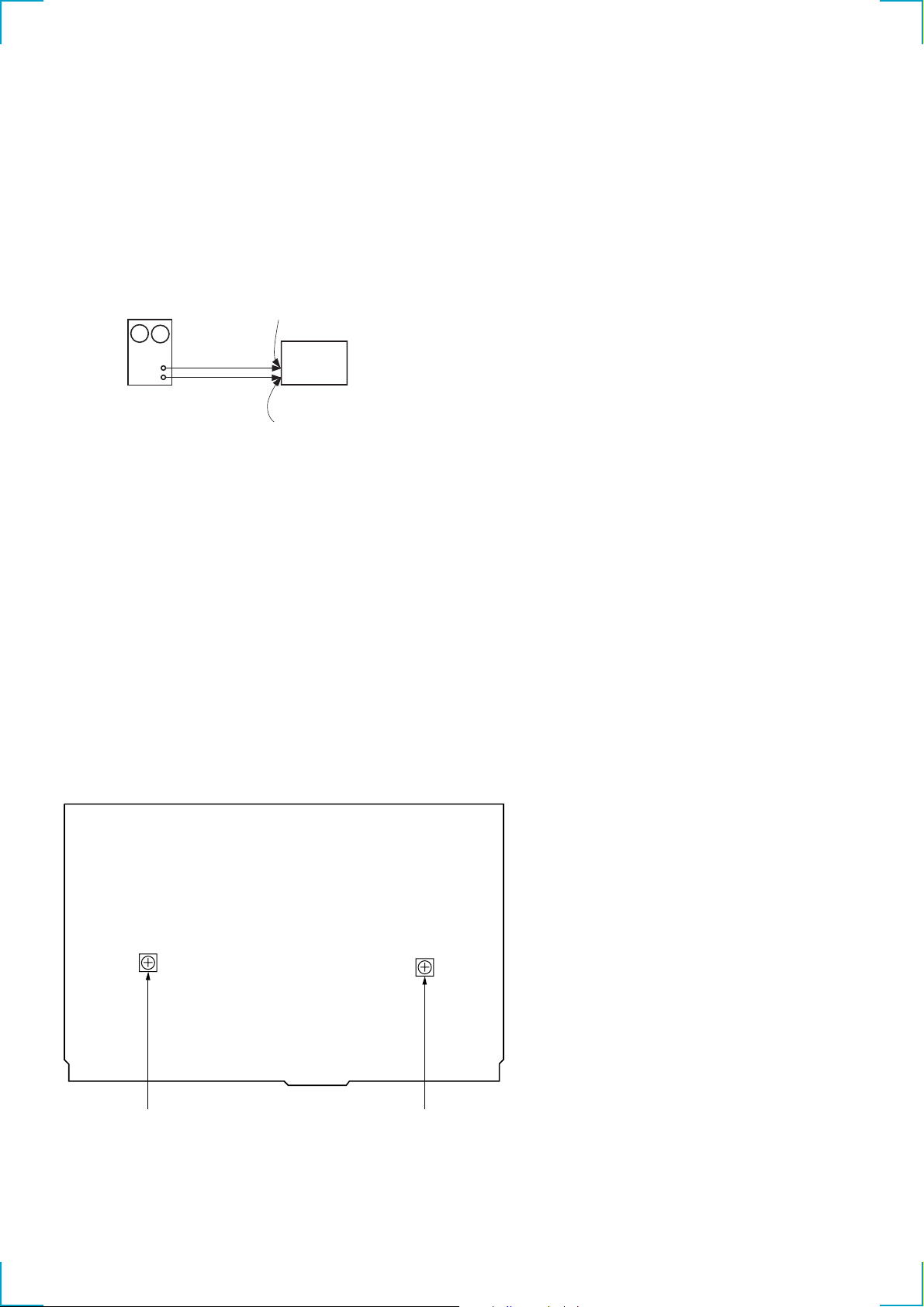
2-1. PLATE, BOTTOM
4 P 2.6x2.8
3 BTP 3x6
6
2 BTP 3x6
1 BTP 3x6
5 plate, bottom
7 sheet, insulating
2-2. MAIN BOARD
2 BTP 3x6
1 BTP 3x6
3 B.TT. 3x14
4 B.TT. 3x14
5 B.TT. 3x14
7 MAIN board section
8 CN808
6
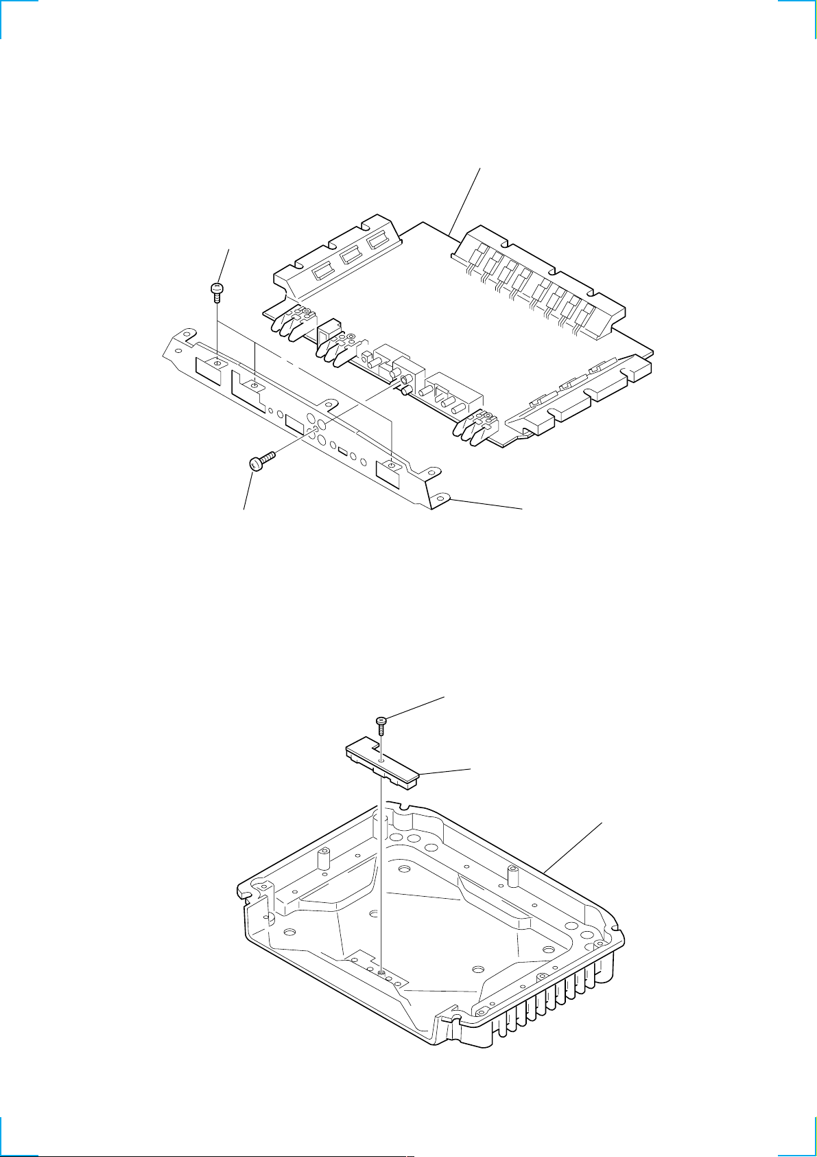
2-3. FRONT PANEL
)
4 MAIN board
2 P 3x8
2-4. LED BOARD
1 P 3x8
3 panel (2ch), front
1 BTP 3x6
2 LED board
heat sink (main
7
l
Ver 1.1
SECTION 3
ELECTRICAL ADJUSTMENT
Bias Adjustment
Note : In Bias Adjustment, adjust RV105 if any of Q108 through
Q113 are replaced. Adjust RV205 if any of Q208 through
Q213 are replaced.
Condition :This adjustment should be performed about one minute
after the remote mode is turned on at a room temperature of about 25°C.
Setting :
B+, REM terminal
set
Stabilized
Power supply
Procedure :
1. Turn the variable resistors RV105 (L-CH) and RV205 (R-CH)
full clockwise as seen from the component side to minimize the
bias current.
2. The input signal is to be no signal.
3. Apply the voltage to the B+ and REM terminals from the stabilized power supply and gradually increase it up to 14.4 V while
checking for any unusual current.
4. For the XM-1502SX, adjust each of R V105 (L-CH) and RV205
(R-CH) so that the power current of the stabilized power supply
is increased in steps of 500 mA (total of 1 A). For the XM1902GX, adjust each of RV105 (L-CH) and RV205 (R-CH) so
that the power current is increased in steps of 600 mA (total of
1.2 A).
5. After adjustment, check that the power current is at 1.3 to 2.0 A.
GND termina
Adjustment Location : Main board (component side)
– MAIN BOARD (COMPONENT SIDE) –
RV105
BIAS ADJUSTMENT
(L-CH)
RV205
BIAS ADJUSTMENT
(R-CH)
8

4-1. BLOCK DIAGRAM
CNJ801-1
INPUT
L
OUTPUT
(THROUGH)
CNJ803
L
HI LEVEL
INPUT
R
CNJ801-2
OUTPUT
(THROUGH)
R
INPUT
S301
TEST TONE
PRE AMP
IC101(1/2)
3
2
PRE AMP
IC201(1/2)
2
3
1
1
TEST TONE
GENERATOR
IC301(2/2)
TEST TONE
GENERATOR
IC301(1/2)
SECTION 4
DIAGRAMS
RV101-1
FILTER
XM-1902GX
RV101-2
FILTER
XM-1902GX
D301
+14.2B
D302
-14.2B
PRE AMP
IC101(2/2)
6
5
PRE AMP
IC201(2/2)
6
5
(B+)
(B–)
H.L.F
IC102(2/2)
7 5 7 2 1 6 7
H.P.F
IC202(2/2)
7 5 7 2 1 2 1
RV801-1
FILTER
RV801-3
FILTER
L.P.F
IC102(1/2)
L.P.F
IC202(1/2)
RV801-2
FILTER
RV801-4
FILTER
L.P.F
IC103(2/2)
L.P.F
IC103(1/2)
S801-2
FILTER
LPF
OFF
HPF
S801-1
FILTER
LPF
OFF
HPF
LOW BOOST
IC104(2/2)
5
6
RV103-1
LOW
BOOST
LOW BOOST
IC204(1/2)
5
6
RV103-2
LOW
BOOST
+14.2V
(B+)
LEVEL
SHIFT
Q101
-14.2V
(B–)
+14.2V
(B+)
LEVEL
SHIFT
Q201
-14.2V
(B–)
XM-1502SX/1902GX
Ver 1.2
LINE AMP
IC104(1/2)
3
7
2
RV104-1
LEVEL
LINE AMP
IC204(2/2)
3
7
2
RV104-2
LEVEL
1
1
LINE SWITCH
CONTROL
Q801,802
LINE
SWITCH
Q102
LINE
SWITCH
Q202
DIFFERENTIAL
AMP
Q103
DIFFERENTIAL
AMP
Q104
DIFFERENTIAL
AMP
Q203
DIFFERENTIAL
AMP
Q204
DRIVE
AMP
Q105
RV105
DRIVE
AMP
Q106
DRIVE
AMP
Q205
RV205
DRIVE
AMP
Q206
BIAS
BIAS
OVER CURRENT
BIAS
Q107
(Q110,111,115:XM-1902GX)
OVER CURRENT
BIAS
Q207
(Q210,211,215:XM-1902GX)
POWER
AMP
Q108,110,112
DET
Q114-116
POWER
AMP
Q109,111,113
POWER
AMP
Q208,210,212
DET
Q214-216
POWER
AMP
Q209,211,213
CN804
CN805
1
2
1
2
SPEAKER
OUT
L
SPEAKER
OUT
R
DC OFFSET
DET
Q803-805
CN802
1
REM
CN801
12V
2
GND
1
+14.2V
(B+)
POWER
04
D808
F901
D809
OVER
CURRENT
D810
OFFSET
Q808
+14.2V
(B+)
D811
THERMAL
D808 D807
LED DRIVE
Q809
POWER
ON/OFF
Q903
B+
SWITCH
Q901,902
LED DRIVE
Q813
PROTECT LATCH
Q812
LED DRIVE
Q811
PROTECT LATCH
Q810
DC DET
IC901
TEMP. DET
TH801-803,
806-809,
812,813
DC-DC CONVERTER
IC901
12
REF.
REG
14
1
2
15
16
3
DC-DC
CONVERTER
TRANSFORMER
T901
11
Q908
Q909
DET
INVERTER
Q904,905
INVERTER
Q906,907
+20.3V
(B+)
-20.3V
(B–)
10
DRIVER
8
9
DRIVER
HI-CURRENT
4
/HI-VOLTAGE
IC903,Q912
DECT
D909
DECT
D905
DECT
D907
DECT
D906
DECT
D908
DECT
D910
• Signal path
: AUDIO
D921
D920
D919
D922
+53V
(B+)
+51V
(B+)
+53V
(B+)
-51V
(B–)
-51V
(B–)
-53V
(B–)
DECT
D911,917
DECT
D912,918
B+
REG
Q910
B+
REG
Q911
+20.3V
(B+)
+14.2V
(B+)
-14.2V
(B–)
-20.3V
(B–)
99

Ver 1.2
THIS NOTE IS COMMON FOR PRINTED WIRING BOARDS
AND SCHEMATIC DIAGRAMS.
(In addition to this, the necessary note is
printed in each block.)
for schematic diagram:
Note:
• All capacitors are in µF unless otherwise noted. pF: µµF
50 WV or less are not indicated except for electrolytics
and tantalums.
• All resistors are in Ω and 1/
specified.
4
W or less unless otherwise
•%: indicates tolerance.
• 2 : nonflammable resistor.
• U : B+ Line.
• V : B– Line.
• Power voltage is dc 14.4V and fed with regulated dc power
supply from +12V and REM terminals.
•Voltage is dc with respect to ground under no-signal
condition.
•Voltages are taken with a VOM (Input impedance 10 MΩ).
Voltage variations may be noted due to normal production tolerances.
•Waveforms are taken with a oscilloscope.
Voltage variations may be noted due to normal production tolerances.
• Circled numbers refer to waveforms.
• Signal path.
F : AUDIO
• Abbreviation
CND : Canadian model
for printed wiring boards:
Note:
• X : parts extracted from the component side.
• : Pattern from the side which enables seeing.
• Abbreviation
CND : Canadian model
• IC Block Diagram
IC901 µPC494GS-T1
16 15 14 13 12 11 10 9
ERROR
ERROR
REF. REG.
0.1V
OSC
• Semiconductor Location (MAIN SECTION)
Ref. No. Location
D101 E-9
D102 E-9
D103 E-9
D104 E-9
D201 E-4
D202 E-3
D203 E-4
D204 E-4
D301 F-8
D302 G-7
D801 D-7
D802 D-7
D803 B-11
D805 A-11
D807 B-11
D820 C-12
D821 D-12
D824 F-12
D825 G-12
D826 C-1
D827 D-1
D830 F-1
D831 G-1
D901 G-10
D902 G-10
D905 A-4
D906 A-4
D907 A-9
D908 A-8
D909 D-5
D910 D-5
D911 D-6
D912 D-5
D913 B-2
D914 B-2
D915 B-3
D917 D-6
D918 D-5
D919 D-10
D920 D-10
D921 E-3
D922 E-3
Ref. No. Location
Q101 F-4
Q102 E-7
Q103 F-9
Q104 F-9
Q105 E-10
Q106 E-10
Q107 G-11
Q108 C-11
Q109 D-11
(Q110) E-11
(Q111) F-11
Q112 F-11
Q113 G-11
Q114 C-12
(Q115) D-12
Q116 F-12
Q201 G-4
Q202 E-5
Q203 E-3
Q204 E-4
Q205 E-3
Q206 E-3
Q207 G-1
Q208 C-1
Q209 D-1
(Q210) E-1
(Q211) E-1
Q212 F-1
Q213 G-1
Q214 D-1
(Q215) D-1
Q216 F-1
Q801 D-7
Q802 D-7
Q803 B-1
Q804 B-1
Q805 B-1
Q809 A-11
Q810 A-12
Q811 A-11
Q812 B-11
Q813 B-11
Q901 F-10
IC101 F-6
IC102 F-5
IC103 F-5
IC104 F-3
IC201 F-6
IC202 G-5
IC204 G-3
IC301 F-8
IC901 B-10
IC902 F-9
IC903 A-10
Q902 F-10
Q903 G-10
Q904 A-8
Q905 A-7
Q906 A-5
Q907 A-6
Q908 A-7
Q909 A-6
Q910 B-2
Q911 B-2
Q912 B-3
( ) : XM-1902GX only
• Waveform
1
10 10
1 2 3 4 5 6 7 8
1V/DIV, 5µsec/DIV
3.4Vp-p
15µsec
IC901
5
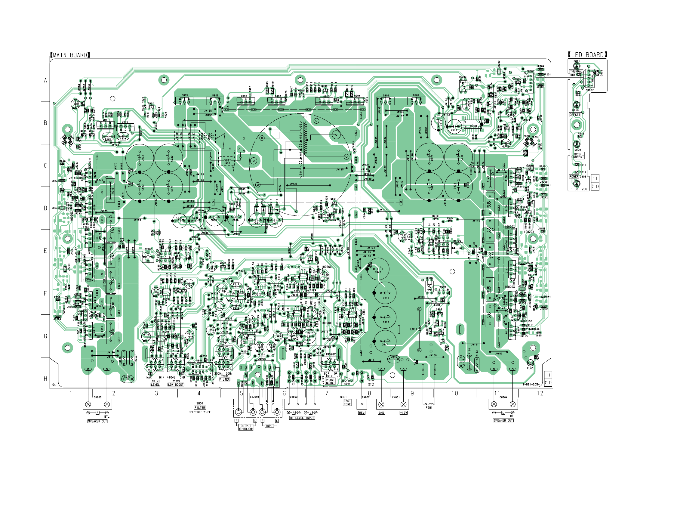
4-2. PRINTED WIRING BOARDS — MAIN SECTION — • Refer to page 10 for Semiconductor Location.
US,CND
MODEL
AEP,UK,E
MODEL
US,CND
MODEL
XM-1502SX/1902GX
Ver 1.2
11 11
 Loading...