

Page 1

XM-1505SX/1805GX
SERVICE MANUAL
Photo: XM-1805GX
SPECIFICATIONS
AUDIO POWER SPECIFICATIONS
POWER OUTPUT AND TOTAL HARMONIC DISTORTION
40 watts/150 watts per channel minimum continuous average power into
4 ohms, 5channels driven from 50 Hz (1505SX), 20 Hz (1805GX) to
20 kHz/20 Hz to 300 Hz (subwoofer) with no more than 0.04% total
harmonic distortion per Car Audio Ad Hoc Committee standards.
US Model
Canadian Model
XM-1505SX/1805GX
E Model
XM-1505SX
Other Specifications
Circuit system OTL (output transformerless) circuit
Pulse power supply
Inputs RCA pin jacks
Outputs Speaker terminals
Through out pin jacks
Speaker impedance 2 – 8 Ω (stereo)
4 – 8 Ω (when used as a bridging amplifier)
1.3 – 8 Ω (only for subwoofer output) (XM-1805GX)
Maximum outputs 80 watts × 4 + 300 watts × 1 (at 4 Ω)
Rated outputs (supply voltage at 14.4 V)
5 Speakers: 1505SX:
40 watts × 4 (50 Hz – 20 kHz, 0.04%
THD, at 4 Ω) + 150 watts × 1 (20 –
300 Hz, 0.04% THD, at 4 Ω)
60 watts × 4 (50 Hz – 20 kHz, 0.1%
THD, at 2 Ω) + 180 watts × 1 (20 –
300 Hz, 0.1% THD, at 2 Ω)
1805GX:
40 watts × 4 (Front: 50 Hz – 20 kHz,
Rear: 20 Hz – 20 kHz, 0.04% THD, at
4 Ω) + 150 watts × 1 (20 – 300 Hz,
0.04% THD, at 4 Ω)
60 watts × 4 (Front: 50 Hz – 20 kHz,
Rear: 20 Hz – 20 kHz, 0.1% THD, at
2 Ω) + 180 watts × 1 (20 – 300 Hz,
0.1% THD, at 2 Ω)
3 Speakers: 120 watts × 2 (50 Hz – 20 kHz, 0.1%
THD, at 4 Ω) + 150 watts × 1 (20 –
300 Hz, 0.04% THD, at 4 Ω)
Frequency response 5 Hz – 50 kHz ( dB)
Harmonic distortion 0.005% or less (at 1 kHz, 4 Ω)
Input level adjustment range
0.2 – 6.0 V (RCA pin jacks)
High-pass filter 50 – 300 Hz, –12 dB/oct
Low-pass filter 50 – 300 Hz, –12 dB/oct
Phase shift adjustment range (XM-1805GX)
0° – 180° (at 40 Hz) (only for subwoofer output)
Power requirements 12 V DC car battery
(negative ground)
Power supply voltage 10.5 – 16 V
Current drain at rated output : 42 A
Remote input : 1.0 mA
Dimensions Approx. 358 × 50 × 264 mm
(w/h/d) (14
projecting parts and controls
Mass Approx. 3.5 kg (7 lb. 11 oz.) not incl. accessories
Supplied accessories Mounting screws (4)
Design and specifications are subject to change without
notice.
+0
–3
1/8 × 2 1/4 × 10 1/2 in.) not incl.
STEREO POWER AMPLIFIER
1
Page 2

SECTION 1
SERVICE NOTE
TABLE OF CONTENTS
1. SERVICE NOTE................................................................. 2
2. GENERAL
Location and Function of Controls.......................................... 3
Connections ............................................................................. 4
3. DISASSEMBLY
3-1. Plate, Bottom ....................................................................... 6
3-2. Amp Board Section ............................................................. 6
3-3. Amp Board, HPF Board, LPF Board................................... 7
3-4. LED Board........................................................................... 7
4. ELECTRICAL ADJUSTMENT...................................... 8
5. DIAGRAMS
5-1. Block Diagram..................................................................... 9
5-2. Printed Wiring Board –Amp Section– ............................... 11
5-3. Schematic Diagram –Amp Section (1/2)–......................... 12
5-4. Schematic Diagram –Amp Section (2/2)–......................... 13
5-5. Printed Wiring Boards –HPF, LPF, LED Section–............ 14
5-6. Schematic Diagram –HPF, LPF, LED Section– ................ 15
6. EXPLODED VIEWS
6-1. Heat Sink (Main) Section .................................................. 16
6-2. Amp Board Section ........................................................... 16
7. ELECTRICAL PARTS LIST......................................... 17
NOTE FOR REPLACEMENT OF Q510 AND Q512
When replacing Q510 and Q512, remove C937 and then remove
the screw securing the heat sink (retainer plate).
heat sink (retainer plate)
C937
Notes on Chip Component Replacement
• Never reuse a disconnected chip component.
• Notice that the minus side of a tantalum capacitor may be dam-
aged by heat.
Q512
Q510
2
Page 3

SECTION 2
GENERAL
This section is extracted
from instruction manual.
3
Page 4

456
Page 5

Page 6
SECTION 3
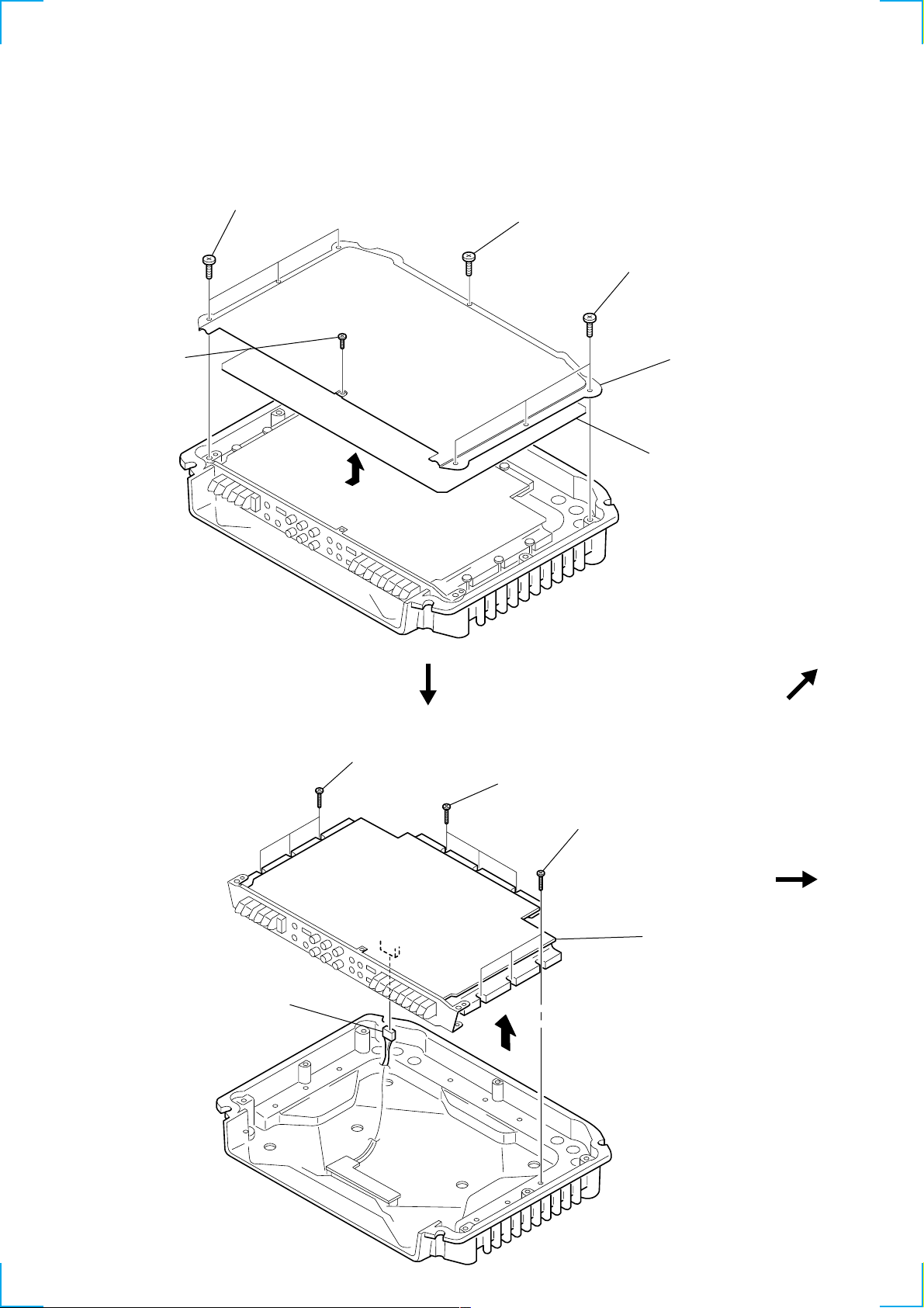
DISASSEMBLY
Note : Follow the disassembly procedure in the numerical order given.
3-1. PLATE, BOTTOM
4 P 2.6x2.8
3 BTP 3x6
6
2 BTP 3x6
1 BTP 3x6
5 plate, bottom
7 sheet, insulating
3-2. AMP BOARD SECTION
6 CNP808
1 B.TT. 3x14
2 B.TT. 3x14
3 B.TT. 3x14
5 AMP board section
4
Page 7

3-3. AMP BOARD, HPF BOARD, LPF BOARD
)
2 P 3x8
6 HPF board
5 CNP806
4 BVTT 3x5
7 BVTT 3x5
9 LPF board
0 AMP board
8 CNP807
3-4. LED BOARD
1 P 3x8
3 panel (5ch), front
1 BTP 3x6
2 LED board
heat sink (main
7
Page 8

SECTION 4
ELECTRICAL ADJUSTMENT
Bias Adjustment
Note : The Bias adjustment should be performed only if any of
Q106, Q107, Q206, Q207, Q306, Q307, Q406, Q407, Q506
Q507 and Q509 to Q512 are replaced.
Setting :
Stabilized
Power supply
B+,REM terminals
set
GND terminal test points
Procedure :
1. Rotate the variable resistors VR101, VR201, VR301, VR401
and VR501 fully in the clockwise direction to minimize the
idling current of the stabilized power supply.
2. The input signal is to be no signal.
3. Set the power voltage to +14.4 V, and turn the remote mode ON
(Connect between the REM terminal and B+ terminal).
4. Connect on digital voltmeter between each test points.
5. Adjust VR101, VR201, VR301 and VR401 so that the digital
voltmeter reading is 5 ± 0.5 mV.
6. Adjust VR501 so that the digital voltmeter reading is
3.5 ± 0.5 mV.
RV Ref. No. Test points
VR101 TP101 and TP102
VR201 TP201 and TP202
VR301 TP301 and TP302
VR401 TP401 and TP402
VR501 TP501 and TP502
Digital
Voltmeter
+
_
Adjustment Location :
– AMP BOARD (COMPONENT SIDE) –
BIAS ADJUSTMENT
BIAS ADJUSTMENT
BIAS ADJUSTMENT
Test Point Location :
– AMP BOARD (CONDUCTOR SIDE) –
TP502
TP501
VR401
BIAS ADJUSTMENT
VR301
VR201
VR101
VR501
BIAS ADJUSTMENT
TP401TP402
TP301
TP302
TP201
TP202
TP101
TP102
8
Page 9

5-1. BLOCK DIAGRAM
XM-1505SX/1805GX
SECTION 5
DIAGRAMS
FRONT
REAR
CNJ805-1
L
CNJ805-2
R
CNJ805-3
L
CNJ805-4
R
PRE AMP
IC801(1/2)
5
6
3
2
5
6
3
2
MODE (SUB WOOFER)
PRE AMP
IC801(2/2)
PRE AMP
IC806(2/2)
PRE AMP
IC806(1/2)
S803
F F+R
7
1
7
1
LEVEL SHIFT
IC802(2/2)
5
6
RV801(1/2)
RV801
LEVEL
(FRONT)
LEVEL SHIFT
IC802(1/2)
3
2
RV801(2/2)
VR803
LEVEL
(REAR)
7
1
LEVEL SHIFT
IC807(2/2)
5
6
VR803(1/2)
LEVEL SHIFT
IC807(1/2)
2
3
VR803(2/2)
S801
HPF
X20
X1
-14.5V
TEST TONE GENERATOR
7
1
7
1
IC805
1805GX
S802
HPF
ON
OFF
12
13
1
10 9 8
1 2 3 4
S851
6
TEST TONE
2
VR804
(2/4)
VR804
(4/4)
HIGH PASS
1505SX
VR804
HPF
(REAR)
1505SX
RV802
(1/4)
FILTER
IC803
RV802
(2/4)
VR804
(2/4)
VR804
(3/4)
RV802
(3/4)
RV802
(4/4)
LINE AMP
IC804(1/2)
3 1
RV802
HPF
(FRONT)
LINE AMP
IC804(2/2)
5 7
LINE AMP
IC808(2/2)
5 7
LINE AMP
IC808(1/2)
3 1
LINE
SWITCH
Q116
LINE
SWITCH
Q216
LINE
SWITCH
Q316
LINE
SWITCH
Q416
DIFFERENTIAL
AMP
Q101
DIFFERENTIAL
AMP
Q102
DIFFERENTIAL
AMP
Q201
DIFFERENTIAL
AMP
Q202
DIFFERENTIAL
AMP
Q301
DIFFERENTIAL
AMP
Q302
DIFFERENTIAL
AMP
Q401
DIFFERENTIAL
AMP
Q402
DRIVE
AMP
Q103
DRIVE
AMP
Q104
DRIVE
AMP
Q203
DRIVE
AMP
Q204
DRIVE
AMP
Q303
DRIVE
AMP
Q304
DRIVE
AMP
Q403
DRIVE
AMP
Q404
VR101
BIAS
VR201
BIAS
VR301
BIAS
VR401
BIAS
BIAS
Q105
BIAS
Q205
BIAS
Q305
BIAS
Q405
POWER
AMP
Q107
POWER
AMP
Q106
POWER
AMP
Q207
POWER
AMP
Q206
POWER
AMP
Q307
POWER
AMP
Q306
POWER
AMP
Q407
POWER
AMP
Q406
OVER LOAD
DET
Q108
OVER LOAD
DET
Q208
OVER LOAD
DET
Q308
OVER LOAD
DET
Q408
CN804
L
BTL
FRONT
R
SPEAKER
OUT
L
BTL
REAR
R
VR805
LEVEL
(SUB WOOFER)
DC-DC
1805GX
RV806
PHASE
10
9
DRIVER
Q911
DRIVER
Q910
PHASE SHIFT
IC810(2/2)
5
6
INVERTER
Q913
INVERTER
Q912
L.P.F AMP
IC810(1/2)
7
RV807
LPF
T902
3 1
DC DET
IC811
D915
D917
D918
D916
MUTE
Q804
B+
(+45V)
B+
(+39V)
B+
(-45V)
B+
(-39V)
LINE
SWITCH
Q516
IC901IC902
12
11
DC-DC
8
CONVERTER
DIFFERENTIAL
AMP
Q501
DIFFERENTIAL
AMP
Q502
LED842
OVER CURRENT
DRIVER
10
DRIVER
9
LED843
OFFSET
Q905
Q904
DRIVE
AMP
Q503
DRIVE
AMP
Q504
INVERTER
Q907
INVERTER
Q906
VR501
BIAS
BIAS
Q505
LED DRIVE
Q802
T901
POWER AMP
Q507,509
(1505SX)
Q507,509,511
(1805GX)
POWER AMP
Q506,510
(1505SX)
Q506,510,512
(1805GX)
LED DRIVE
Q803
D905
D907
D906
D908
OVER LOAD
OFFSET DET
Q805-807
B+ REG
Q909
B- REG
Q908
DET
Q508
B+
(+30V)
B+
(+14.5V)
B-
(-14.5V)
B-
(-30V)
CN803
SUB WOOFER
SPEAKER OUT
L+R
• Signal path
: AUDIO
PRE AMP
CNJ805-5
L
SUB
WOOFER
CNJ805-6
R
B-
(-45V)
CN801
+12V
GND
CN802
REM
04
F901
2
1
IC809(1/2)
3
2
DC DET
Q914
REG
Q901,902
POWER
ON/OFF
Q903
SWITCH
Q841
B+
(+39V)
1
D841
THERMAL
LED
DRIVE
Q801
DC DET
IC903
D844
POWER
TH803-
805
LEVELAMP
IC809(2/2)
5
6
7
12
11
8
CONVERTER
16
14
99
Page 10

THIS NOTE IS COMMON FOR PRINTED WIRING BOARDS
AND SCHEMATIC DIAGRAMS.
(In addition to this, the necessary note is
printed in each block.)
for schematic diagram:
Note:
• All capacitors are in µF unless otherwise noted. pF: µµF
50 WV or less are not indicated except for electrolytics
and tantalums.
• All resistors are in Ω and 1/
specified.
4
W or less unless otherwise
• % : indicates tolerance.
• 2 : nonflammable resistor.
• U : B+ Line.
• V : B– Line.
• Power voltage is dc 14.4V and fed with regulated dc power
supply from +12V and REMOTE terminals.
• Voltage is dc with respect to ground under no-signal
condition.
• Voltages are taken with a VOM (Input impedance 10 MΩ).
Voltage variations may be noted due to normal production tolerances.
• Signal path.
F : AUDIO
for printed wiring boards:
Note:
• X : parts extracted from the component side.
• b : Pattern from the side which enables seeing.
(The other layer’s patterns are not indicated.)
• IC Block Diagram
IC901, 902 µPC494GS-T
16 15 14 13 12 11 10 9
ERROR
ERROR
1 2 3 4 5 6 7 8
REF. REG.
0.1V
OSC
• Semiconductor Location (AMP SECTION)
Ref. No. Location Ref. No. Location
D506 F-3
D507 F-3
D801 D-8
D802 B-4
D803 F-8
D804 F-7
D805 E-8
D806 E-8
D807 B-4
D901 F-5
D902 F-5
D903 D-6
D904 D-6
D905 B-8
D906 B-8
D907 B-9
D908 B-9
D909 B-12
D910 B-12
D911 F-9
D912 F-9
D913 D-5
D914 D-5
D915 D-4
D916 D-4
D917 C-2
D918 B-2
D919 F-4
D920 F-4
D921 E-5
D922 E-5
D923 E-5
D928 E-5
Q205 E-14
Q206 E-14
Q207 D-14
Q208 F-13
Q216 F-12
Q301 C-12
Q302 C-12
Q303 C-13
Q304 D-13
Q305 C-14
Q306 D-14
Q307 C-14
Q308 D-13
Q316 D-11
Q401 C-11
Q402 C-11
Q403 C-10
Q404 C-11
Q405 B-11
Q406 B-11
Q407 B-10
Q408 B-11
Q416 D-11
Q501 F-4
Q502 F-4
Q503 G-4
Q504 F-4
Q505 F-2
Q506 E-2
Q507 F-2
Q508 F-3
Q509 G-2
Q510 E-2
Q511 H-2
IC801 H-8
IC806 H-7
IC807 H-8
IC808 H-10
IC809 H-6
IC811 E-7
IC901 D-7
IC902 D-5
IC903 E-5
Q512 D-2
Q516 G-6
Q801 F-7
Q802 G-8
Q803 G-9
Q804 F-8
Q805 F-9
Q806 G-9
Q807 G-9
Q901 F-5
Q101 G-12
Q102 G-12
Q103 F-13
Q104 G-13
Q105 G-14
Q106 G-14
Q107 F-14
Q108 G-13
Q116 G-12
Q201 E-12
Q202 E-12
Q203 E-13
Q204 E-13
Q902 G-5
Q903 F-5
Q904 E-6
Q905 D-6
Q906 B-7
Q907 B-6
Q908 F-9
Q909 F-9
Q910 E-5
Q911 D-5
Q912 B-6
Q913 B-5
Q914 F-5
10 10
Page 11

5-2. PRINTED WIRING BOARD — AMP SECTION — • Refer to page 10 for Semiconductor Location.
XM-1505SX/1805GX
A
B
C
D
E
F
G
H
I
J
1
3
LED BOARD
CNJ808
(Page 14)
AMP BOARD
Q505
PL801
04
2 3 4 5 6 7 8 9 1011121314
Q407
R439
R430
Q403
R423
Q401
R432
R434
R426
R419
Q416
1805GX
R438
R437
R428
R427
VR401
C1 C2
B1 B2E
C416
C415
R317
R
R422
R417
Q405
Q406
C953
R425
Q402
C1 C2
B1 B2E
R420
C414
C419
C418
JR16
R433
R431
R435
TP402
Q408
BCE
Q404
R436
C417
R421
R429
JR29
R424
C314
R318
R319
C313
Q316
R217
Q216
R219
Q116
C113
C319R338
R337
BTL BTL
L R L
D909
D910
Q303
R323
R326
B1
E
R322
B2C1C2
R320
B1
E
R324
C2C1C2
R321
R329
C317
R223
R226
B1
E
R222
B2C1C2
B1
R220
E
C2C1C2
R224
R221
R229
C217
C951
C214
C950
R123
R117
R126
B1
E
R122
CN804
R120
R124
B2C1C2
B1
E
C2C1C2
R121
R129
C117
R238
C114
R118
R119
SPEAKER OUTREAR FRONT
Q302
Q203
Q202
Q102
Q301
C316
C315
R325
Q304
R336
Q201
C216
C215
R225
Q204
R236
Q103
C116
C115
R125
Q104
R136
Q101
C924
JR15
JR14
Q208
JR13
Q108
C219
Q308
BCE
C923
BCE
BCE
R339
R239
R234
C218
R139
R134
R334
TP102
TP302
R335
R235
TP101
C118
R135
TP301
R332
R330
VR301
C318
R333
R331
TP201
R232
R230
VR201
TP202
R231
R233
R132
R130
VR101
R133
R131
Q307
Q207
Q107
TH801
R137
R327
R227
R127
Q305
Q306
Q205
Q206
Q105
Q106
C119R138
R328
R228
R128
1-680-818-
D918
D917
JW180
C943
1805GX
C820
R541
Q512
C942
Q510
TP502
Q507
R539
Q506
TH805
R528
R532
R527
TP501
VR501
Q509
R540
1805GX
Q511
R538
CN803 CN801
L+R
SUB WOOFER
SPEAKER OUT
JR32
R533
TH804
C519
C515
C518
R542
R537
JR1
C934
D507
JW181
C937C936
Q508
R535
D506
R530
R534
JR27
REM
BCE
R531
R544
JR28
R902
C902
L903
TP3
R901
R900
C935
R545
JR21
TP2
TP1
D802
R847
R846
D807
C938 C939
D919
D920
Q504
R529
R521
R547
Q502
C2C1B2
R524
E
B1
R520
C2C1B2
R525 JR22
R522
E
B1
C518
Q501
R526
R523
R546
Q503
C901
GNDCN802
+12V
R929
Q913 Q912 Q907 Q906
JR20
JR19
R803
D916D915
Q911
ECB
R927
D913
C941C940
D922
D921
D928
R536
R519
D901
C514
BCE
Q902
L901
R932
R904
R903
F901
40A
BCE
JR30
R931
Q903
BCE
JR26
R905
D914
Q910
R922
D923
BCE
Q914
R906
Q901
2
LPF BOARD
CNJ807
R930
R941
R843
TH903
C932
C931
C927
R923
R924
R925
IC902
R928
34
IC903
21
R907
D902
C819
R840
(SUB WOOFER) (REAR)
C926
18
189
C928
R921
C930
C929
TH901
C933
JR3
15
R834
C503
R504
R506
VR805
LEVEL
R944
R942
R926
Q516
CNP807
C815
R601
R501
C505
C504
R503
R505
JR40
R502
R602
14
85
IC809
C506
JR2
S803
MODE
(SUB WOOFER)
F+R F
R915
R937
R939
C909
Q905
BCE
R913
BCE
Q904
C910
C405
R401 R404
R403
C502
C602
C818
R837
RLRLRL
SUB WOOFER
D903
D904
4
C403
R402
C501
R914
C404
R405
C304
C305
R305
C601
R911
IC901
C907
R517
1
85
C904
IC806
R440
C402
R938
TH802
R910
R303
189
43
12
IC811
C303
R203
R302
R340
C401
R940
R909
18
JR11
R304
R301
REAR
INPUT
JR17
Q801
C301
C817
R836
JR18
C905
C205
C903
D804
C802
R204
R201
C302
R916
T901T902
R912
R908
C807
D805
C1 E2B2
E1 C2B1
R821
Q804
R807
R805
C1 E2B2
E1 C2B1
R808
R809
CNP808
JR4
4
C203
R202
C105
R240
C201
CNJ805
R801
C906
R806
C204
R205
C104
R105
C202
D801
R802
15
1
85
C103
D806
C801
R838
IC801
R102
R104
R833
D906
R822
R820
C806
R103
R140
C814
C101
C816
R835
FRONT
C918
R823
JR41
R101
R814
R816
R819
D803
R815
C1 E2B2
E1 C2B1
R818
R306
C813
JR34
R811
Q802
R817
R832
R308
C917
D905
JW71
C102
C919
R839
Q803
C804
R307
R406
JR6JR5
C306
R408
VR803
LEVEL
(REAR)
C914
C913
R917
Q909
D911
C803
C406
14
85
JR33
C408
C409
R311
1505SX
VR804
HPF
R827
-3
-4
-1
-2
C916
C915
R918
C920
R824
R920
D912
R829
R410
R310
D908
JW65
Q908
R828
R826
C1 E2B2
E1 C2B1
C810
IC808
C308
JR36
ON OFF
R831
C948
C309
JR35
S802
HPF
D907
JW64
JW63
L902
R919
C921
Q805
BCE
R825
JR12
R810
C1 E2B2
C1 E2B2
E1 C2B1
E1 C2B1
R812
R813
Q806
R407
R207
110
R206
R106
R107
IC807
JR8
JR7
-1
R411
-2
(REAR)
C952
TP401
JW66
C911
C912
C922
R830
Q807
C812
C949
CN806
C307
R309C410
R414
C310
R314
R313
R312
-1
-2
C407
JR10
R409
JR9
1805GX
R413
14
85
R412 R237
1
HPF BOARD
CNJ806
(Page 14)(Page 14)
11
11 11
Page 12

XM-1505SX/1805GX
5-3. SCHEMATIC DIAGRAM — AMP SECTION (1/2) —
(Page 15)
(Page 15)
(Page 15)
(Page 15)
(Page 13)
12 12
Page 13

5-4. SCHEMATIC DIAGRAM — AMP SECTION (2/2) — • Refer to page 10 for IC Block Diagram.
XM-1505SX/1805GX
(Page 12)
(Page 15)
• Waveform
1V/DIV, 5µsec/DIV
1
3.4Vp-p
13 13
15µsec
IC901, 902
5
Page 14

XM-1505SX/1805GX
5-5. PRINTED WIRING BOARDS — HPF, LPF, LED SECTION —
A
B
C
D
E
F
04
1
2 3 4 5 6 7 8 9 10 11 12
(Page 11)
AMP BOARD
(Page 11)
AMP BOARD
CNP806
CNP807
2
1
LPF BOARD
CNJ807
1505SX
C508
41
IC810
58
-1
-2
R510
RV807
LPF
1505SX
R509
R507
JR31
R508
1805GX
15
JR37
1-680-821-
RV806
PHASE
C507
11
D924
D925
1805GX
TEST TONE
JR25
R935
S851
R934
D927
D926
R215
R933
14 8
IC803
17
C212
R216
IC804
85
1
C112
R115
R116
S801
HPF
(FRONT)
X1 X20
1805GX
4
CNJ806
C111
R214
R213
R113
C211
R212
R114
110
C110
R112
C210
-4
-2
-1
-3
RV802
HPF
(FRONT)
1805GX
C109
C209
R211
R111
C108
C208
1805GX
R209
-1
R936
R208
R108
(FRONT)
R861
-2
RV801
LEVEL
HPF BOARD
C853
R859
R857
IC805
C851
85
D851
R851
R852
C106
R109
85
14
IC802
C206
R858
R860
C853
R862
14
C854
JR23
JR24
R854
R855
R853
C852
R856
C509
R511
111-680-820-
04
G
H
J
(Page 11)
AMP BOARD
CNP808
3
Q841
CBE
15
CNJ808
R841
I
LED841
THERMAL
04
R843
LED843
OFFSET
LED BOARD
OVER CURRENT
POWER/PROTECTOR
R842
LED842
R844
1-680-819-
R845
11
LED844
POWER
14 14
Page 15

5-6. SCHEMATIC DIAGRAM — HPF, LPF, LED SECTION —
XM-1505SX/1805GX
(Page 12)
(Page 12)
(Page 12)
(Page 13)
(Page 12)
15 15
Page 16

NOTE:
• The mechanical parts with no reference
number in the exploded views are not supplied.
• Items marked “*” are not stocked since
they are seldom required for routine service.
Some delay should be anticipated
when ordering these items.
SECTION 6
EXPLODED VIEWS
• Color Indication of Appearance Parts
Example :
KNOB, BALANCE (WHITE) ... (RED)
RR
Parts Color Cabinet’s Color
• Accessories and packing materials and
hardware (# mark) list are given in
the last of this parts list.
6-2. AMP BOARD SECTION
#4
6-1. HEAT SINK (MAIN) SECTION
#4
61
60
62
1
62
56
54
58
53
55
57
55
8
55
58
1505SX
2
#5
58
54
67
64
7
7
3
#3
4
A
59
A
5
#1
65
66
68
54
53
59
55
58
54
52
1805GX
53
57
59
F901
Ref. No. Part No. Description Remark Ref. No. Part No. Description Remark
1 3-225-070-21 PLATE (HEAT SINK), ORNAMENTAL (1805GX)
1 3-225-079-21 PLATE (HEAT SINK), ORNAMENTAL
1 3-225-079-61 PLATE (HEAT SINK), ORNAMENTAL (1505SX:E)
* 2 3-225-071-01 HEAT SINK (MAIN)
* 3 3-225-065-01 HOLDER, LED
7
6
#1
(1505SX:US,CND)
#1
#2
* 4 1-680-819-11 LED BOARD
* 5 3-225-081-01 SHEET, INSULATING
* 6 3-225-068-01 PLATE, BOTTOM
7 3-225-185-01 SCREW (+B.TT.3X14)
8 3-225-153-01 SHEET (HEAT SINK), ADHESIVE
F901 1-532-947-11 FUSE (BLADE TYPE) (AUTO FUSE) 30A
#1
#3
63
Ref. No. Part No. Description Remark Ref. No. Part No. Description Remark
* 51 A-3326-994-A AMP BOARD, COMPLETE (1505SX)
* 51 A-3340-000-A AMP BOARD, COMPLETE (1805GX)
* 52 3-225-067-01 HEAT SINK (SUB 2)
53 3-225-183-01 SCREW (+PSW.TT.3XL)
* 54 3-225-080-01 HEAT SINK (RETAINER PLATE)
55 3-225-183-11 SCREW (+PSW.TT.3XL)
* 56 3-225-066-01 HEAT SINK (SUB 1)
* 57 3-226-618-01 HEAT SINK (SUB 3)
* 58 3-225-086-01 SHEET (TR), INSULATING
59 3-225-184-01 SCREW (+PS.TT.3X6)
* 61 A-3326-995-A HPF BOARD, COMPLETE (1505SX)
* 61 A-3326-998-A HPF BOARD, COMPLETE (1805GX)
* 62 3-225-076-01 BRACKET (5CH.VR3)
63 3-225-075-01 PANEL (5CH), FRONT (1805GX)
63 3-225-075-11 PANEL (5CH), FRONT (1505SX)
64 3-912-431-01 SCREW (P)
65 3-369-647-01 SCREW (M4 SPACER)
66 3-912-432-01 SCREW (B)
* 67 3-225-078-01 BRACKET (5CH.VR1)
* 68 3-225-077-01 BRACKET (5CH.VR2)
51
* 60 1-680-821-11 LPF BOARD
16 16
Page 17

SECTION 7
ELECTRICAL PARTS LIST
NOTE:
• Due to standardization, replacements in
the parts list may be different from the
parts specified in the diagrams or the
components used on the set.
• RESISTORS
All resistors are in ohms.
METAL:Metal-film resistor.
METAL OXIDE: Metal oxide-film resistor.
F:nonflammable
Ref. No. Part No. Description Remark Ref. No. Part No. Description Remark
* A-3326-994-A AMP BOARD, COMPLETE (1505SX)
* A-3340-000-A AMP BOARD, COMPLETE (1805GX)
*********************
* 3-225-066-01 HEAT SINK (SUB 1)
* 3-225-067-01 HEAT SINK (SUB 2)
* 3-225-077-01 BRACKET (5CH.VR2)
* 3-225-078-01 BRACKET (5CH.VR1)
* 3-225-080-01 HEAT SINK (RETAINER PLATE)
* 3-225-086-01 SHEET (TR), INSULATING
3-225-183-01 SCREW (+PSW.TT.3XL)
3-225-183-11 SCREW (+PSW.TT.3XL)
3-225-184-01 SCREW (+PS.TT.3X6)
* 3-226-618-01 HEAT SINK (SUB 3)
7-685-646-79 SCREW +P 3X8 TYPE2 NON-SLIT
7-685-544-19 SCREW +BTP 3X5 TYPE2 N-S
• Items marked “*” are not stocked since
they are seldom required for routine service.
Some delay should be anticipated
when ordering these items.
• SEMICONDUCTORS
In each case, u : µ, for example:
uA.. : µA.. uPA.. : µPA..
uPB.. : µPB.. uPC.. : µPC.. uPD.. : µPD..
• CAPACITORS
uF : µF
• COILS
uH : µH
C305 1-162-923-11 CERAMIC CHIP 47PF 5% 50V
C306 1-164-230-11 CERAMIC CHIP 220PF 5% 50V
C307 1-126-157-11 ELECT 10uF 20% 16V
C308 1-136-169-00 MYLAR 0.22uF 5% 50V
C309 1-136-169-00 MYLAR 0.22uF 5% 50V
C310 1-162-927-11 CERAMIC CHIP 100PF 5% 50V
C313 1-126-022-11 ELECT 47uF 20% 25V
C314 1-126-049-11 ELECT 22uF 20% 50V
C315 1-162-915-11 CERAMIC CHIP 10PF 0.5PF 50V
C316 1-107-826-11 CERAMIC CHIP 0.1uF 10% 16V
C317 1-107-826-11 CERAMIC CHIP 0.1uF 10% 16V
C318 1-136-165-00 MYLAR 0.1uF 5% 50V
C319 1-136-161-00 MYLAR 0.047uF 5% 50V
C401 1-126-047-21 ELECT 4.7uF 20% 50V
C402 1-126-047-21 ELECT 4.7uF 20% 50V
When indicating parts by reference
number, please include the board.
AMP
(1805GX)
< CAPACITOR >
C101 1-126-047-21 ELECT 4.7uF 20% 50V
C102 1-126-047-21 ELECT 4.7uF 20% 50V
C103 1-162-927-11 CERAMIC CHIP 100PF 5% 50V
C104 1-162-927-11 CERAMIC CHIP 100PF 5% 50V
C105 1-162-923-11 CERAMIC CHIP 47PF 5% 50V
C113 1-126-022-11 ELECT 47uF 20% 25V
C114 1-126-049-11 ELECT 22uF 20% 50V
C115 1-162-915-11 CERAMIC CHIP 10PF 0.5PF 50V
C116 1-107-826-11 CERAMIC CHIP 0.1uF 10% 16V
C117 1-107-826-11 CERAMIC CHIP 0.1uF 10% 16V
C118 1-136-165-00 MYLAR 0.1uF 5% 50V
C119 1-136-161-00 MYLAR 0.047uF 5% 50V
C201 1-126-047-21 ELECT 4.7uF 20% 50V
C202 1-126-047-21 ELECT 4.7uF 20% 50V
C203 1-162-927-11 CERAMIC CHIP 100PF 5% 50V
C204 1-162-927-11 CERAMIC CHIP 100PF 5% 50V
C205 1-162-923-11 CERAMIC CHIP 47PF 5% 50V
C214 1-126-022-11 ELECT 47uF 20% 25V
C215 1-162-915-11 CERAMIC CHIP 10PF 0.5PF 50V
C216 1-107-826-11 CERAMIC CHIP 0.1uF 10% 16V
C217 1-107-826-11 CERAMIC CHIP 0.1uF 10% 16V
C218 1-136-165-00 MYLAR 0.1uF 5% 50V
C219 1-136-161-00 MYLAR 0.047uF 5% 50V
C301 1-126-047-21 ELECT 4.7uF 20% 50V
C302 1-126-047-21 ELECT 4.7uF 20% 50V
C303 1-162-927-11 CERAMIC CHIP 100PF 5% 50V
C304 1-162-927-11 CERAMIC CHIP 100PF 5% 50V
C403 1-162-927-11 CERAMIC CHIP 100PF 5% 50V
C404 1-162-927-11 CERAMIC CHIP 100PF 5% 50V
C405 1-162-923-11 CERAMIC CHIP 47PF 5% 50V
C406 1-164-230-11 CERAMIC CHIP 220PF 5% 50V
C407 1-126-157-11 ELECT 10uF 20% 16V
(1805GX)
C408 1-136-169-00 MYLAR 0.22uF 5% 50V
C409 1-136-169-00 MYLAR 0.22uF 5% 50V
C410 1-162-927-11 CERAMIC CHIP 100PF 5% 50V
C414 1-126-022-11 ELECT 47uF 20% 25V
C415 1-162-915-11 CERAMIC CHIP 10PF 0.5PF 50V
C416 1-107-826-11 CERAMIC CHIP 0.1uF 10% 16V
C417 1-107-826-11 CERAMIC CHIP 0.1uF 10% 16V
C418 1-136-165-00 MYLAR 0.1uF 5% 50V
C419 1-136-161-00 MYLAR 0.047uF 5% 50V
C501 1-126-047-21 ELECT 4.7uF 20% 50V
C502 1-126-047-21 ELECT 4.7uF 20% 50V
C503 1-162-927-11 CERAMIC CHIP 100PF 5% 50V
C504 1-162-927-11 CERAMIC CHIP 100PF 5% 50V
C505 1-162-923-11 CERAMIC CHIP 47PF 5% 50V
C506 1-164-230-11 CERAMIC CHIP 220PF 5% 50V
C514 1-126-022-11 ELECT 47uF 20% 25V
C515 1-136-153-00 FILM 0.01uF 5% 50V
C516 1-136-157-00 MYLAR 0.022uF 5% 50V
C518 1-136-165-00 MYLAR 0.1uF 5% 50V
C519 1-136-161-00 MYLAR 0.047uF 5% 50V
C601 1-126-047-21 ELECT 4.7uF 20% 50V
C602 1-126-047-21 ELECT 4.7uF 20% 50V
C801 1-107-826-11 CERAMIC CHIP 0.1uF 10% 16V
17
Page 18

AMP
Ref. No. Part No. Description Remark Ref. No. Part No. Description Remark
C802 1-162-970-11 CERAMIC CHIP 0.01uF 10% 25V
C803 1-162-962-11 CERAMIC CHIP 470PF 10% 50V
C804 1-126-049-11 ELECT 22uF 20% 50V
C805 1-162-962-11 CERAMIC CHIP 470PF 10% 50V
C806 1-126-044-11 ELECT 1uF 20% 50V
C940 1-126-063-11 ELECT 100uF 20% 63V
C941 1-126-063-11 ELECT 100uF 20% 63V
C942 1-162-964-11 CERAMIC CHIP 0.001uF 10% 50V
C943 1-162-964-11 CERAMIC CHIP 0.001uF 10% 50V
C948 1-162-970-11 CERAMIC CHIP 0.01uF 10% 25V
C807 1-126-049-11 ELECT 22uF 20% 50V
C810 1-126-022-11 ELECT 47uF 20% 25V
C812 1-126-022-11 ELECT 47uF 20% 25V
C813 1-126-024-11 ELECT 220uF 20% 16V
C814 1-126-044-11 ELECT 1uF 20% 50V
C815 1-126-044-11 ELECT 1uF 20% 50V
C816 1-165-128-11 CERAMIC CHIP 0.22uF 16V
C817 1-165-128-11 CERAMIC CHIP 0.22uF 16V
C818 1-165-128-11 CERAMIC CHIP 0.22uF 16V
C819 1-162-970-11 CERAMIC CHIP 0.01uF 10% 25V
C820 1-107-826-11 CERAMIC CHIP 0.1uF 10% 16V
C901 1-136-173-00 MYLAR 0.47uF 5% 50V
C902 1-162-964-11 CERAMIC CHIP 0.001uF 10% 50V
C903 1-162-970-11 CERAMIC CHIP 0.01uF 10% 25V
C904 1-162-964-11 CERAMIC CHIP 0.001uF 10% 50V
C905 1-126-022-11 ELECT 47uF 20% 25V
C906 1-126-049-11 ELECT 22uF 20% 50V
C907 1-126-009-81 ELECT 100uF 20% 16V
C909 1-131-731-11 ELECT 2200uF 20% 16V
C910 1-131-731-11 ELECT 2200uF 20% 16V
C911 1-136-165-00 MYLAR 0.1uF 5% 50V
C912 1-136-165-00 MYLAR 0.1uF 5% 50V
C913 1-115-819-11 ELECT 2200uF 20% 35V
C914 1-115-819-11 ELECT 2200uF 20% 35V
C915 1-115-819-11 ELECT 2200uF 20% 35V
C916 1-115-819-11 ELECT 2200uF 20% 35V
C917 1-126-052-11 ELECT 100uF 20% 35V
C918 1-126-052-11 ELECT 100uF 20% 35V
C919 1-126-047-21 ELECT 4.7uF 20% 50V
C920 1-126-047-21 ELECT 4.7uF 20% 50V
C921 1-126-009-81 ELECT 100uF 20% 16V
C922 1-126-009-81 ELECT 100uF 20% 16V
C923 1-162-964-11 CERAMIC CHIP 0.001uF 10% 50V
C924 1-162-964-11 CERAMIC CHIP 0.001uF 10% 50V
C926 1-107-715-11 ELECT 22uF 20% 16V
C927 1-162-964-11 CERAMIC CHIP 0.001uF 10% 50V
C928 1-126-022-11 ELECT 47uF 20% 25V
C929 1-126-049-11 ELECT 22uF 20% 50V
C930 1-126-009-81 ELECT 100uF 20% 16V
C931 1-136-153-00 FILM 0.01uF 5% 50V
C932 1-131-731-11 ELECT 2200uF 20% 16V
C933 1-131-731-11 ELECT 2200uF 20% 16V
C934 1-136-165-00 MYLAR 0.1uF 5% 50V
C935 1-136-165-00 MYLAR 0.1uF 5% 50V
C936 1-115-454-51 ELECT 1500uF 20% 50V
C937 1-115-454-51 ELECT 1500uF 20% 50V
C938 1-115-454-51 ELECT 1500uF 20% 50V
C939 1-115-454-51 ELECT 1500uF 20% 50V
C949 1-162-970-11 CERAMIC CHIP 0.01uF 10% 25V
C950 1-126-044-11 ELECT 1uF 20% 50V
C951 1-126-044-11 ELECT 1uF 20% 50V
C952 1-126-044-11 ELECT 1uF 20% 50V
C953 1-126-044-11 ELECT 1uF 20% 50V
< TERMINAL BOARD >
CN801 1-694-755-11 TERMINAL BOARD (2P+FUSE) (+12V,GND)
CN803 1-694-754-11 TERMINAL BOARD (2P) (SUB WOOFER
SPEAKER OUT)
CN804 1-694-752-11 TERMINAL BOARD (8P) (SPEAKER OUT)
< JACK >
CN805 1-794-852-11 JACK, PIN 6P (INPUT)
< CONNECTOR >
CN802 1-815-300-11 CONNECTOR (REMOTE) 1P (REM)
CNP806 1-815-524-11 CONNECTOR, BOARD TO BOARD 10P
CNP807 1-815-522-11 CONNECTOR, BOARD TO BOARD 5P
CNP808 1-506-987-11 PIN, CONNECTOR (PC BOARD) 5P
< DIODE >
D506 8-719-978-65 DIODE DTZ-TT11-15B
D507 8-719-978-65 DIODE DTZ-TT11-15B
D801 8-719-801-78 DIODE 1SS184
D802 8-719-801-78 DIODE 1SS184
D803 8-719-801-78 DIODE 1SS184
D804 8-719-801-78 DIODE 1SS184
D805 8-719-978-33 DIODE DTZ-TT11-6.8B
D806 8-719-016-74 DIODE 1SS352
D807 8-719-801-78 DIODE 1SS184
D901 8-719-025-50 DIODE 02CZ16-TE85L
D902 8-719-978-33 DIODE DTZ-TT11-6.8B
D903 8-719-016-74 DIODE 1SS352
D904 8-719-016-74 DIODE 1SS352
D905 8-719-054-55 DIODE 1SS306(TE85L)
D906 8-719-054-55 DIODE 1SS306(TE85L)
D907 8-719-076-60 DIODE FCH20A15
D908 8-719-076-61 DIODE FRH20A15
D909 8-719-016-74 DIODE 1SS352
D910 8-719-016-74 DIODE 1SS352
D911 8-719-025-49 DIODE 02CZ15-TE85L
D912 8-719-025-49 DIODE 02CZ15-TE85L
D913 8-719-016-74 DIODE 1SS352
D914 8-719-016-74 DIODE 1SS352
D915 8-719-054-55 DIODE 1SS306(TE85L)
D916 8-719-054-55 DIODE 1SS306(TE85L)
D917 8-719-079-00 DIODE FCH10A15
18
Page 19

AMP
Ref. No. Part No. Description Remark Ref. No. Part No. Description Remark
D918 8-719-079-01 DIODE FRH10A15
D919 8-719-016-74 DIODE 1SS352
D920 8-719-016-74 DIODE 1SS352
D921 8-719-025-51 DIODE 02CZ18-TE85L
D922 8-719-025-51 DIODE 02CZ18-TE85L
D923 8-719-025-51 DIODE 02CZ18-TE85L
D928 8-719-025-51 DIODE 02CZ18-TE85L
< IC >
JR36 1-216-864-11 METAL CHIP 0 5% 1/16W
(1505SX)
JR40 1-216-864-11 METAL CHIP 0 5% 1/16W
JR41 1-216-296-11 SHORT 0
< DIODE >
JR5 8-719-977-12 DIODE DTZ6.8B
JR6 8-719-977-12 DIODE DTZ6.8B
JW71 8-719-901-33 DIODE 1SS133
IC801 8-759-711-82 IC NJM4580E(T1)
IC806 8-759-711-82 IC NJM4580E(T1)
IC807 8-759-711-82 IC NJM4580E(T1)
IC808 8-759-711-82 IC NJM4580E(T1)
IC809 8-759-711-82 IC NJM4580E(T1)
IC901 8-759-144-88 IC uPC494GS-T1
IC902 8-759-144-88 IC uPC494GS-T1
< PHOTO COUPLER >
IC811 8-719-156-72 PHOTO COUPLER PS2501-1-K
IC903 8-719-156-72 PHOTO COUPLER PS2501-1-K
< JUMPER RESISTOR >
JR1 1-216-296-11 SHORT 0
JR2 1-216-864-11 METAL CHIP 0 5% 1/16W
JR3 1-216-864-11 METAL CHIP 0 5% 1/16W
JR4 1-216-296-11 SHORT 0
JR7 1-216-296-11 SHORT 0
JR8 1-216-864-11 METAL CHIP 0 5% 1/16W
JR9 1-216-296-11 SHORT 0
JR10 1-216-296-11 SHORT 0
JR11 1-216-864-11 METAL CHIP 0 5% 1/16W
JR12 1-216-864-11 METAL CHIP 0 5% 1/16W
JR13 1-216-296-11 SHORT 0
JR14 1-216-296-11 SHORT 0
JR15 1-216-296-11 SHORT 0
JR16 1-216-296-11 SHORT 0
JR17 1-216-864-11 METAL CHIP 0 5% 1/16W
JR18 1-216-296-11 SHORT 0
JR19 1-216-296-11 SHORT 0
JR20 1-216-296-11 SHORT 0
JR21 1-216-864-11 METAL CHIP 0 5% 1/16W
JR22 1-216-296-11 SHORT 0
JR26 1-216-864-11 METAL CHIP 0 5% 1/16W
JR27 1-216-864-11 METAL CHIP 0 5% 1/16W
JR28 1-216-864-11 METAL CHIP 0 5% 1/16W
JR29 1-216-296-11 SHORT 0
JR30 1-216-864-11 METAL CHIP 0 5% 1/16W
JR32 1-216-296-11 SHORT 0
JR33 1-216-864-11 METAL CHIP 0 5% 1/16W
JR34 1-216-864-11 METAL CHIP 0 5% 1/16W
JR35 1-216-864-11 METAL CHIP 0 5% 1/16W
(1505SX)
< FERRITE BEAD >
JW63 1-410-396-41 INDUCTOR, FERRITE BEAD 0.45uH
JW64 1-410-396-41 INDUCTOR, FERRITE BEAD 0.45uH
JW65 1-410-396-41 INDUCTOR, FERRITE BEAD 0.45uH
JW66 1-410-396-41 INDUCTOR, FERRITE BEAD 0.45uH
JW180 1-410-396-41 INDUCTOR, FERRITE BEAD 0.45uH
JW181 1-410-396-41 INDUCTOR, FERRITE BEAD 0.45uH
L901 1-424-719-11 COIL, CHOKE (EI-35)
L902 1-410-396-41 INDUCTOR, FERRITE BEAD 0.45uH
L903 1-410-396-41 INDUCTOR, FERRITE BEAD 0.45uH
< PILOT LAMP >
PL801 1-518-540-11 LAMP, PILOT (50mA/18V)
< TRANSISTOR >
Q101 8-729-014-86 TRANSISTOR 2SC4207-YGRTE85L
Q102 8-729-014-85 TRANSISTOR 2SA1618-YGRTE85R
Q103 8-729-140-82 TRANSISTOR 2SA988-PAFAEA
Q104 8-729-184-53 TRANSISTOR 2SC1845-EA
Q105 8-729-055-13 TRANSISTOR 2SD1861-TV2
Q106 8-729-053-85 FET IRF9540
Q107 8-729-015-42 FET IRFI540
Q108 8-729-230-49 TRANSISTOR 2SC2712-YG
Q116 8-729-203-48 TRANSISTOR 2SC3327-A
Q201 8-729-014-86 TRANSISTOR 2SC4207-YGRTE85L
Q202 8-729-014-85 TRANSISTOR 2SA1618-YGRTE85R
Q203 8-729-140-82 TRANSISTOR 2SA988-PAFAEA
Q204 8-729-184-53 TRANSISTOR 2SC1845-EA
Q205 8-729-055-13 TRANSISTOR 2SD1861-TV2
Q206 8-729-053-85 FET IRF9540
Q207 8-729-015-42 FET IRFI540
Q208 8-729-230-49 TRANSISTOR 2SC2712-YG
Q216 8-729-203-48 TRANSISTOR 2SC3327-A
Q301 8-729-014-86 TRANSISTOR 2SC4207-YGRTE85L
Q302 8-729-014-85 TRANSISTOR 2SA1618-YGRTE85R
Q303 8-729-140-82 TRANSISTOR 2SA988-PAFAEA
Q304 8-729-184-53 TRANSISTOR 2SC1845-EA
Q305 8-729-055-13 TRANSISTOR 2SD1861-TV2
Q306 8-729-053-85 FET IRF9540
Q307 8-729-015-42 FET IRFI540
Q308 8-729-230-49 TRANSISTOR 2SC2712-YG
Q316 8-729-203-48 TRANSISTOR 2SC3327-A
Q401 8-729-014-86 TRANSISTOR 2SC4207-YGRTE85L
19
Page 20

AMP
Ref. No. Part No. Description Remark Ref. No. Part No. Description Remark
Q402 8-729-014-85 TRANSISTOR 2SA1618-YGRTE85R
Q403 8-729-140-82 TRANSISTOR 2SA988-PAFAEA
Q404 8-729-184-53 TRANSISTOR 2SC1845-EA
Q405 8-729-055-13 TRANSISTOR 2SD1861-TV2
Q406 8-729-053-85 FET IRF9540
R119 1-216-829-11 METAL CHIP 4.7K 5% 1/16W
R120 1-216-835-11 METAL CHIP 15K 5% 1/16W
R121 1-216-829-11 METAL CHIP 4.7K 5% 1/16W
R122 1-216-835-11 METAL CHIP 15K 5% 1/16W
R123 1-216-829-11 METAL CHIP 4.7K 5% 1/16W
Q407 8-729-015-42 FET IRFI540
Q408 8-729-230-49 TRANSISTOR 2SC2712-YG
Q416 8-729-203-48 TRANSISTOR 2SC3327-A
Q501 8-729-926-22 TRANSISTOR FMW3
Q502 8-729-055-75 TRANSISTOR FMS3
Q503 8-729-209-18 TRANSISTOR 2SA1360-Y
Q504 8-729-203-45 TRANSISTOR 2SC3423-O
Q505 8-729-055-13 TRANSISTOR 2SD1861-TV2
Q506 8-729-053-85 FET IRF9540
Q507 8-729-015-42 FET IRFI540
Q508 8-729-230-49 TRANSISTOR 2SC2712-YG
Q509 8-729-015-42 FET IRFI540
Q510 8-729-053-85 FET IRF9540
Q511 8-729-015-42 FET IRFI540 (1805GX)
Q512 8-729-053-85 FET IRF9540 (1805GX)
Q516 8-729-203-48 TRANSISTOR 2SC3327-A
Q801 8-729-049-77 TRANSISTOR HN1B01F-GR(T5LSONY)
Q802 8-729-049-77 TRANSISTOR HN1B01F-GR(T5LSONY)
Q803 8-729-049-77 TRANSISTOR HN1B01F-GR(T5LSONY)
Q804 8-729-049-77 TRANSISTOR HN1B01F-GR(T5LSONY)
Q805 8-729-230-49 TRANSISTOR 2SC2712-YG
Q806 8-729-049-77 TRANSISTOR HN1B01F-GR(T5LSONY)
Q807 8-729-049-77 TRANSISTOR HN1B01F-GR(T5LSONY)
Q901 8-729-048-66 TRANSISTOR 2SB1238PQR-TV2
Q902 8-729-216-21 TRANSISTOR 2SA1162-Y
R124 1-216-829-11 METAL CHIP 4.7K 5% 1/16W
R125 1-208-494-61 RES-CHIP 2.2K 2% 1/8W
R126 1-216-813-11 METAL CHIP 220 5% 1/16W
R127 1-216-835-11 METAL CHIP 15K 5% 1/16W
R128 1-216-833-11 METAL CHIP 10K 5% 1/16W
R129 1-216-813-11 METAL CHIP 220 5% 1/16W
R130 1-216-845-11 METAL CHIP 100K 5% 1/16W
R131 1-216-845-11 METAL CHIP 100K 5% 1/16W
R132 1-216-809-11 METAL CHIP 100 5% 1/16W
R133 1-216-809-11 METAL CHIP 100 5% 1/16W
R134 1-216-819-11 METAL CHIP 680 5% 1/16W
R135 1-216-821-11 METAL CHIP 1K 5% 1/16W
R136 1-216-833-11 METAL CHIP 10K 5% 1/16W
R137 1-216-853-11 METAL CHIP 470K 5% 1/16W
R138 1-215-857-11 METAL OXIDE 10 5% 1W F
R139 1-205-991-11 METAL 0.1X2
R140 1-216-821-11 METAL CHIP 1K 5% 1/16W
R201 1-216-837-11 METAL CHIP 22K 5% 1/16W
R202 1-216-837-11 METAL CHIP 22K 5% 1/16W
R203 1-220-397-11 RES-CHIP 4.7M 5% 1/16W
R204 1-216-837-11 METAL CHIP 22K 5% 1/16W
R205 1-216-837-11 METAL CHIP 22K 5% 1/16W
R206 1-216-821-11 METAL CHIP 1K 5% 1/16W
R207 1-216-825-11 METAL CHIP 2.2K 5% 1/16W
R217 1-216-837-11 METAL CHIP 22K 5% 1/16W
Q903 8-729-230-49 TRANSISTOR 2SC2712-YG
Q904 8-729-901-98 TRANSISTOR 2SA1036K-R
Q905 8-729-901-98 TRANSISTOR 2SA1036K-R
Q906 8-729-053-05 FET FKV550T
Q907 8-729-053-05 FET FKV550T
Q908 8-729-141-83 TRANSISTOR 2SB1094-LK
Q909 8-729-209-15 TRANSISTOR 2SD2012
Q910 8-729-901-98 TRANSISTOR 2SA1036K-R
Q911 8-729-901-98 TRANSISTOR 2SA1036K-R
Q912 8-729-053-05 FET FKV550T
Q913 8-729-053-05 FET FKV550T
Q914 8-729-230-49 TRANSISTOR 2SC2712-YG
< RESISTOR >
R101 1-216-837-11 METAL CHIP 22K 5% 1/16W
R102 1-216-837-11 METAL CHIP 22K 5% 1/16W
R103 1-220-397-11 RES-CHIP 4.7M 5% 1/16W
R104 1-216-837-11 METAL CHIP 22K 5% 1/16W
R105 1-216-837-11 METAL CHIP 22K 5% 1/16W
R106 1-216-821-11 METAL CHIP 1K 5% 1/16W
R107 1-216-825-11 METAL CHIP 2.2K 5% 1/16W
R117 1-216-837-11 METAL CHIP 22K 5% 1/16W
R118 1-216-829-11 METAL CHIP 4.7K 5% 1/16W
R219 1-216-829-11 METAL CHIP 4.7K 5% 1/16W
R220 1-216-835-11 METAL CHIP 15K 5% 1/16W
R221 1-216-829-11 METAL CHIP 4.7K 5% 1/16W
R222 1-216-835-11 METAL CHIP 15K 5% 1/16W
R223 1-216-829-11 METAL CHIP 4.7K 5% 1/16W
R224 1-216-829-11 METAL CHIP 4.7K 5% 1/16W
R225 1-216-210-00 RES-CHIP 3.3K 2% 1/8W
R226 1-216-813-11 METAL CHIP 220 5% 1/16W
R227 1-216-835-11 METAL CHIP 15K 5% 1/16W
R228 1-216-833-11 METAL CHIP 10K 5% 1/16W
R229 1-216-813-11 METAL CHIP 220 5% 1/16W
R230 1-216-845-11 METAL CHIP 100K 5% 1/16W
R231 1-216-845-11 METAL CHIP 100K 5% 1/16W
R232 1-216-809-11 METAL CHIP 100 5% 1/16W
R233 1-216-809-11 METAL CHIP 100 5% 1/16W
R234 1-216-819-11 METAL CHIP 680 5% 1/16W
R235 1-216-821-11 METAL CHIP 1K 5% 1/16W
R236 1-216-833-11 METAL CHIP 10K 5% 1/16W
R237 1-216-853-11 METAL CHIP 470K 5% 1/16W
R238 1-215-857-11 METAL OXIDE 10 5% 1W F
R239 1-205-991-11 METAL 0.1X2
R240 1-216-821-11 METAL CHIP 1K 5% 1/16W
R301 1-216-837-11 METAL CHIP 22K 5% 1/16W
20
Page 21

AMP
Ref. No. Part No. Description Remark Ref. No. Part No. Description Remark
R302 1-216-837-11 METAL CHIP 22K 5% 1/16W
R303 1-220-397-11 RES-CHIP 4.7M 5% 1/16W
R304 1-216-837-11 METAL CHIP 22K 5% 1/16W
R305 1-216-837-11 METAL CHIP 22K 5% 1/16W
R306 1-216-821-11 METAL CHIP 1K 5% 1/16W
R414 1-216-829-11 METAL CHIP 4.7K 5% 1/16W
R417 1-216-837-11 METAL CHIP 22K 5% 1/16W
R419 1-216-829-11 METAL CHIP 4.7K 5% 1/16W
R420 1-216-835-11 METAL CHIP 15K 5% 1/16W
R421 1-216-829-11 METAL CHIP 4.7K 5% 1/16W
R307 1-216-825-11 METAL CHIP 2.2K 5% 1/16W
R308 1-216-809-11 METAL CHIP 100 5% 1/16W
R309 1-216-833-11 METAL CHIP 10K 5% 1/16W
(1805GX)
R310 1-216-825-11 METAL CHIP 2.2K 5% 1/16W
R311 1-216-825-11 METAL CHIP 2.2K 5% 1/16W
R312 1-216-853-11 METAL CHIP 470K 5% 1/16W
(1805GX)
R313 1-216-833-11 METAL CHIP 10K 5% 1/16W
R314 1-216-829-11 METAL CHIP 4.7K 5% 1/16W
R317 1-216-837-11 METAL CHIP 22K 5% 1/16W
R318 1-216-829-11 METAL CHIP 4.7K 5% 1/16W
R319 1-216-829-11 METAL CHIP 4.7K 5% 1/16W
R320 1-216-835-11 METAL CHIP 15K 5% 1/16W
R321 1-216-829-11 METAL CHIP 4.7K 5% 1/16W
R322 1-216-835-11 METAL CHIP 15K 5% 1/16W
R323 1-216-829-11 METAL CHIP 4.7K 5% 1/16W
R324 1-216-829-11 METAL CHIP 4.7K 5% 1/16W
R325 1-208-494-61 RES-CHIP 2.2K 2% 1/8W
R326 1-216-813-11 METAL CHIP 220 5% 1/16W
R327 1-216-835-11 METAL CHIP 15K 5% 1/16W
R328 1-216-833-11 METAL CHIP 10K 5% 1/16W
R329 1-216-813-11 METAL CHIP 220 5% 1/16W
R330 1-216-845-11 METAL CHIP 100K 5% 1/16W
R331 1-216-845-11 METAL CHIP 100K 5% 1/16W
R332 1-216-809-11 METAL CHIP 100 5% 1/16W
R333 1-216-809-11 METAL CHIP 100 5% 1/16W
R334 1-216-819-11 METAL CHIP 680 5% 1/16W
R335 1-216-821-11 METAL CHIP 1K 5% 1/16W
R336 1-216-833-11 METAL CHIP 10K 5% 1/16W
R337 1-216-853-11 METAL CHIP 470K 5% 1/16W
R338 1-215-857-11 METAL OXIDE 10 5% 1W F
R339 1-205-991-11 METAL 0.1X2
R340 1-216-821-11 METAL CHIP 1K 5% 1/16W
R401 1-216-837-11 METAL CHIP 22K 5% 1/16W
R402 1-216-837-11 METAL CHIP 22K 5% 1/16W
R403 1-220-397-11 RES-CHIP 4.7M 5% 1/16W
R404 1-216-837-11 METAL CHIP 22K 5% 1/16W
R405 1-216-837-11 METAL CHIP 22K 5% 1/16W
R406 1-216-821-11 METAL CHIP 1K 5% 1/16W
R407 1-216-825-11 METAL CHIP 2.2K 5% 1/16W
R408 1-216-809-11 METAL CHIP 100 5% 1/16W
R409 1-216-833-11 METAL CHIP 10K 5% 1/16W
(1805GX)
R410 1-216-825-11 METAL CHIP 2.2K 5% 1/16W
R411 1-216-825-11 METAL CHIP 2.2K 5% 1/16W
R412 1-216-853-11 METAL CHIP 470K 5% 1/16W
(1805GX)
R413 1-216-833-11 METAL CHIP 10K 5% 1/16W
R422 1-216-835-11 METAL CHIP 15K 5% 1/16W
R423 1-216-829-11 METAL CHIP 4.7K 5% 1/16W
R424 1-216-829-11 METAL CHIP 4.7K 5% 1/16W
R425 1-216-210-00 RES-CHIP 3.3K 2% 1/8W
R426 1-216-813-11 METAL CHIP 220 5% 1/16W
R427 1-216-835-11 METAL CHIP 15K 5% 1/16W
R428 1-216-833-11 METAL CHIP 10K 5% 1/16W
R429 1-216-813-11 METAL CHIP 220 5% 1/16W
R430 1-216-845-11 METAL CHIP 100K 5% 1/16W
R431 1-216-845-11 METAL CHIP 100K 5% 1/16W
R432 1-216-809-11 METAL CHIP 100 5% 1/16W
R433 1-216-809-11 METAL CHIP 100 5% 1/16W
R434 1-216-819-11 METAL CHIP 680 5% 1/16W
R435 1-216-821-11 METAL CHIP 1K 5% 1/16W
R436 1-216-833-11 METAL CHIP 10K 5% 1/16W
R437 1-216-853-11 METAL CHIP 470K 5% 1/16W
R438 1-215-857-11 METAL OXIDE 10 5% 1W F
R439 1-205-991-11 METAL 0.1X2
R440 1-216-821-11 METAL CHIP 1K 5% 1/16W
R501 1-216-837-11 METAL CHIP 22K 5% 1/16W
R502 1-216-837-11 METAL CHIP 22K 5% 1/16W
R503 1-220-397-11 RES-CHIP 4.7M 5% 1/16W
R504 1-216-833-11 METAL CHIP 10K 5% 1/16W
R505 1-216-833-11 METAL CHIP 10K 5% 1/16W
R506 1-216-809-11 METAL CHIP 100 5% 1/16W
R517 1-216-837-11 METAL CHIP 22K 5% 1/16W
R519 1-216-829-11 METAL CHIP 4.7K 5% 1/16W
R520 1-216-841-11 METAL CHIP 47K 5% 1/16W
R521 1-216-829-11 METAL CHIP 4.7K 5% 1/16W
R522 1-216-841-11 METAL CHIP 47K 5% 1/16W
R523 1-216-829-11 METAL CHIP 4.7K 5% 1/16W
R524 1-216-829-11 METAL CHIP 4.7K 5% 1/16W
R525 1-208-510-61 RES-CHIP 10K 2% 1/8W
R526 1-216-813-11 METAL CHIP 220 5% 1/16W
R527 1-216-835-11 METAL CHIP 15K 5% 1/16W
R528 1-216-833-11 METAL CHIP 10K 5% 1/16W
R529 1-216-813-11 METAL CHIP 220 5% 1/16W
R530 1-216-845-11 METAL CHIP 100K 5% 1/16W
R531 1-216-845-11 METAL CHIP 100K 5% 1/16W
R532 1-216-809-11 METAL CHIP 100 5% 1/16W
R533 1-216-809-11 METAL CHIP 100 5% 1/16W
R534 1-216-820-11 METAL CHIP 820 5% 1/16W
(1805GX)
R534 1-216-824-11 METAL CHIP 1.8K 5% 1/16W
(1505SX)
R535 1-216-821-11 METAL CHIP 1K 5% 1/16W
R536 1-216-833-11 METAL CHIP 10K 5% 1/16W
R537 1-216-853-11 METAL CHIP 470K 5% 1/16W
21
Page 22

AMP
Ref. No. Part No. Description Remark Ref. No. Part No. Description Remark
R538 1-215-857-11 METAL OXIDE 10 5% 1W F
R539 1-216-809-11 METAL CHIP 100 5% 1/16W
R540 1-216-809-11 METAL CHIP 100 5% 1/16W
R541 1-216-809-11 METAL CHIP 100 5% 1/16W
(1805GX)
R542 1-216-809-11 METAL CHIP 100 5% 1/16W
(1805GX)
R544 1-244-300-11 METAL 0.22X2 F
R545 1-244-300-11 METAL 0.22X2 F
R546 1-244-300-11 METAL 0.22X2 F
(1805GX)
R547 1-216-809-11 METAL CHIP 100 5% 1/16W
R601 1-216-837-11 METAL CHIP 22K 5% 1/16W
R602 1-216-837-11 METAL CHIP 22K 5% 1/16W
R801 1-216-823-11 METAL CHIP 1.5K 5% 1/16W
R802 1-216-831-11 METAL CHIP 6.8K 5% 1/16W
R803 1-216-823-11 METAL CHIP 1.5K 5% 1/16W
R805 1-216-837-11 METAL CHIP 22K 5% 1/16W
R806 1-216-829-11 METAL CHIP 4.7K 5% 1/16W
R807 1-216-849-11 METAL CHIP 220K 5% 1/16W
R808 1-216-833-11 METAL CHIP 10K 5% 1/16W
R809 1-216-833-11 METAL CHIP 10K 5% 1/16W
R810 1-216-833-11 METAL CHIP 10K 5% 1/16W
R811 1-216-833-11 METAL CHIP 10K 5% 1/16W
R812 1-216-829-11 METAL CHIP 4.7K 5% 1/16W
R813 1-208-510-61 RES-CHIP 10K 2% 1/8W
R814 1-216-845-11 METAL CHIP 100K 5% 1/16W
R815 1-216-833-11 METAL CHIP 10K 5% 1/16W
R816 1-216-833-11 METAL CHIP 10K 5% 1/16W
R817 1-216-829-11 METAL CHIP 4.7K 5% 1/16W
R818 1-208-510-61 RES-CHIP 10K 2% 1/8W
R819 1-216-857-11 METAL CHIP 1M 5% 1/16W
R820 1-216-833-11 METAL CHIP 10K 5% 1/16W
R821 1-216-821-11 METAL CHIP 1K 5% 1/16W
R822 1-216-845-11 METAL CHIP 100K 5% 1/16W
R823 1-216-837-11 METAL CHIP 22K 5% 1/16W
R824 1-216-833-11 METAL CHIP 10K 5% 1/16W
R825 1-216-833-11 METAL CHIP 10K 5% 1/16W
R826 1-216-833-11 METAL CHIP 10K 5% 1/16W
R827 1-216-833-11 METAL CHIP 10K 5% 1/16W
R828 1-216-833-11 METAL CHIP 10K 5% 1/16W
R829 1-216-857-11 METAL CHIP 1M 5% 1/16W
R830 1-216-833-11 METAL CHIP 10K 5% 1/16W
R831 1-216-857-11 METAL CHIP 1M 5% 1/16W
R832 1-216-214-00 RES-CHIP 4.7K 2% 1/8W
R833 1-216-214-00 RES-CHIP 4.7K 2% 1/8W
R834 1-216-214-00 RES-CHIP 4.7K 2% 1/8W
R835 1-216-821-11 METAL CHIP 1K 5% 1/16W
R846 1-216-823-11 METAL CHIP 1.5K 5% 1/16W
R847 1-216-823-11 METAL CHIP 1.5K 5% 1/16W
R900 1-208-510-61 RES-CHIP 10K 2% 1/8W
R901 1-216-833-11 METAL CHIP 10K 5% 1/16W
R902 1-216-833-11 METAL CHIP 10K 5% 1/16W
R903 1-216-214-00 RES-CHIP 4.7K 2% 1/8W
R904 1-216-190-00 RES-CHIP 470 2% 1/8W
R905 1-216-190-00 RES-CHIP 470 2% 1/8W
R906 1-216-190-00 RES-CHIP 470 2% 1/8W
R907 1-216-829-11 METAL CHIP 4.7K 5% 1/16W
R908 1-216-833-11 METAL CHIP 10K 5% 1/16W
R909 1-216-833-11 METAL CHIP 10K 5% 1/16W
R910 1-216-835-11 METAL CHIP 15K 5% 1/16W
R911 1-216-834-11 METAL CHIP 12K 5% 1/16W
R912 1-216-849-11 METAL CHIP 220K 5% 1/16W
R913 1-216-821-11 METAL CHIP 1K 5% 1/16W
R914 1-216-821-11 METAL CHIP 1K 5% 1/16W
R915 1-216-805-11 METAL CHIP 47 5% 1/16W
R916 1-216-805-11 METAL CHIP 47 5% 1/16W
R917 1-216-829-11 METAL CHIP 4.7K 5% 1/16W
R918 1-216-829-11 METAL CHIP 4.7K 5% 1/16W
R919 1-216-829-11 METAL CHIP 4.7K 5% 1/16W
R920 1-216-829-11 METAL CHIP 4.7K 5% 1/16W
R921 1-216-833-11 METAL CHIP 10K 5% 1/16W
R922 1-216-817-11 METAL CHIP 470 5% 1/16W
R923 1-216-833-11 METAL CHIP 10K 5% 1/16W
R924 1-216-835-11 METAL CHIP 15K 5% 1/16W
R925 1-216-834-11 METAL CHIP 12K 5% 1/16W
R926 1-216-849-11 METAL CHIP 220K 5% 1/16W
R927 1-216-821-11 METAL CHIP 1K 5% 1/16W
R928 1-216-821-11 METAL CHIP 1K 5% 1/16W
R929 1-216-805-11 METAL CHIP 47 5% 1/16W
R930 1-216-805-11 METAL CHIP 47 5% 1/16W
R931 1-216-829-11 METAL CHIP 4.7K 5% 1/16W
R932 1-216-813-11 METAL CHIP 220 5% 1/16W
R937 1-208-473-11 RES-CHIP 300 2% 1/8W
R938 1-208-473-11 RES-CHIP 300 2% 1/8W
R939 1-208-473-11 RES-CHIP 300 2% 1/8W
R940 1-208-473-11 RES-CHIP 300 2% 1/8W
R941 1-208-473-11 RES-CHIP 300 2% 1/8W
R942 1-208-473-11 RES-CHIP 300 2% 1/8W
R943 1-208-473-11 RES-CHIP 300 2% 1/8W
R944 1-208-473-11 RES-CHIP 300 2% 1/8W
< SWITCH >
S802 1-572-185-11 SWITCH, SLIDE (HPF (REAR)) (1805GX)
S803 1-572-185-11 SWITCH, SLIDE (MODE (SUB WOOFER))
R836 1-216-821-11 METAL CHIP 1K 5% 1/16W
R837 1-216-821-11 METAL CHIP 1K 5% 1/16W
R838 1-216-833-11 METAL CHIP 10K 5% 1/16W
R839 1-216-841-11 METAL CHIP 47K 5% 1/16W
R840 1-208-494-61 RES-CHIP 2.2K 2% 1/8W
22
< TRANSFORMER >
T901 1-435-931-11 TRANSFORMER, DC-DC CONVERTER
T902 1-435-932-11 TRANSFORMER, DC-DC CONVERTER
Page 23

AMP
Ref. No. Part No. Description Remark Ref. No. Part No. Description Remark
< THERMISTOR >
TH801 1-809-664-51 THERMISTOR, POSITIVE
TH802 1-808-877-11 THERMISTOR
TH804 1-808-877-11 THERMISTOR
TH805 1-808-877-11 THERMISTOR
TH901 1-804-301-11 THERMISTOR (SMD)
C851 1-162-970-11 CERAMIC CHIP 0.01uF 10% 25V
C852 1-162-970-11 CERAMIC CHIP 0.01uF 10% 25V
C853 1-162-970-11 CERAMIC CHIP 0.01uF 10% 25V
C854 1-162-970-11 CERAMIC CHIP 0.01uF 10% 25V
C855 1-107-826-11 CERAMIC CHIP 0.1uF 10% 16V
< CONNECTOR >
HPF
TH903 1-808-877-11 THERMISTOR
< VARIABLE RESISTOR >
VR101 1-241-761-11 RES, ADJ, CERMET 1K
VR201 1-241-761-11 RES, ADJ, CERMET 1K
VR301 1-241-761-11 RES, ADJ, CERMET 1K
VR401 1-241-761-11 RES, ADJ, CERMET 1K
VR501 1-241-761-11 RES, ADJ, CERMET 1K
VR803 1-225-648-11 RES, VAR, CARBON 5KX2 (LEVEL (REAR))
VR804 1-225-647-11 RES, VAR, CARBON 20KX4 (HPF (REAR))
VR805 1-225-648-11 RES, VAR, CARBON 5KX2
(LEVEL (SUB WOOFER))
*************************************************************
* A-3326-995-A HPF BOARD, COMPLETE (1505SX)
* A-3326-998-A HPF BOARD, COMPLETE (1805GX)
********************
* 3-225-076-01 BRACKET (5CH.VR3)
< CAPACITOR >
C106 1-164-230-11 CERAMIC CHIP 220PF 5% 50V
C108 1-136-169-00 MYLAR 0.22uF 5% 50V
(1805GX)
C109 1-136-153-00 FILM 0.01uF 5% 50V
(1805GX)
C109 1-136-169-00 MYLAR 0.22uF 5% 50V
(1505SX)
C110 1-136-153-00 FILM 0.01uF 5% 50V
(1805GX)
C110 1-136-169-00 MYLAR 0.22uF 5% 50V
(1505SX)
C111 1-136-169-00 MYLAR 0.22uF 5% 50V
(1805GX)
C112 1-162-927-11 CERAMIC CHIP 100PF 5% 50V
C206 1-164-230-11 CERAMIC CHIP 220PF 5% 50V
C208 1-136-169-00 MYLAR 0.22uF 5% 50V
(1805GX)
C209 1-136-153-00 FILM 0.01uF 5% 50V
(1805GX)
C209 1-136-169-00 MYLAR 0.22uF 5% 50V
(1505SX)
C210 1-136-153-00 FILM 0.01uF 5% 50V
(1805GX)
C210 1-136-169-00 MYLAR 0.22uF 5% 50V
(1505SX)
C211 1-136-169-00 MYLAR 0.22uF 5% 50V
(1805GX)
C212 1-162-927-11 CERAMIC CHIP 100PF 5% 50V
CNJ806 1-815-523-11 CONNECTOR, BOARD TO BOARD 10P
< DIODE >
D851 8-719-801-78 DIODE 1SS184
D924 8-719-056-85 DIODE UDZS-TE17-8.2B (1805GX)
D925 8-719-056-85 DIODE UDZS-TE17-8.2B (1805GX)
D926 8-719-800-76 DIODE 1SS226-TE85R (1805GX)
D927 8-719-800-76 DIODE 1SS226-TE85R (1805GX)
< IC >
IC802 8-759-711-82 IC NJM4580E(T1)
IC803 8-759-008-67 IC TC4066BF-TP1 (1805GX)
IC804 8-759-711-82 IC NJM4580E(T1)
IC805 8-759-924-46 IC BA4560F-T1
< JUMPER RESISTOR >
JR23 1-216-864-11 METAL CHIP 0 5% 1/16W
(1805GX)
JR23 8-719-977-12 DIODE DTZ6.8B (1505SX)
JR24 1-216-864-11 METAL CHIP 0 5% 1/16W
(1805GX)
JR24 8-719-977-12 DIODE DTZ6.8B (1505SX)
JR25 1-216-864-11 METAL CHIP 0 5% 1/16W
(1805GX)
< RESISTOR >
R108 1-216-809-11 METAL CHIP 100 5% 1/16W
R109 1-216-809-11 METAL CHIP 100 5% 1/16W
(1805GX)
R109 1-216-864-11 METAL CHIP 0 5% 1/16W
(1505SX)
R111 1-216-857-11 METAL CHIP 1M 5% 1/16W
(1805GX)
R112 1-216-857-11 METAL CHIP 1M 5% 1/16W
(1805GX)
R113 1-216-825-11 METAL CHIP 2.2K 5% 1/16W
R114 1-216-825-11 METAL CHIP 2.2K 5% 1/16W
R115 1-216-833-11 METAL CHIP 10K 5% 1/16W
R116 1-216-829-11 METAL CHIP 4.7K 5% 1/16W
R208 1-216-809-11 METAL CHIP 100 5% 1/16W
R209 1-216-809-11 METAL CHIP 100 5% 1/16W
(1805GX)
R209 1-216-864-11 METAL CHIP 0 5% 1/16W
(1505SX)
R211 1-216-857-11 METAL CHIP 1M 5% 1/16W
(1805GX)
R212 1-216-857-11 METAL CHIP 1M 5% 1/16W
(1805GX)
R213 1-216-825-11 METAL CHIP 2.2K 5% 1/16W
23
Page 24

HPF
Ref. No. Part No. Description Remark Ref. No. Part No. Description Remark
R214 1-216-825-11 METAL CHIP 2.2K 5% 1/16W
R215 1-216-833-11 METAL CHIP 10K 5% 1/16W
R216 1-216-829-11 METAL CHIP 4.7K 5% 1/16W
R851 1-216-833-11 METAL CHIP 10K 5% 1/16W
R852 1-216-835-11 METAL CHIP 15K 5% 1/16W
R853 1-216-829-11 METAL CHIP 4.7K 5% 1/16W
R854 1-216-829-11 METAL CHIP 4.7K 5% 1/16W
R855 1-216-845-11 METAL CHIP 100K 5% 1/16W
R856 1-216-833-11 METAL CHIP 10K 5% 1/16W
R857 1-216-833-11 METAL CHIP 10K 5% 1/16W
LED LPF
* 1-680-821-11 LPF BOARD
**********
* 3-225-076-01 BRACKET (5CH.VR3)
< CAPACITOR >
C507 1-126-044-11 ELECT 1uF 20% 50V
(1805GX)
C508 1-136-165-00 MYLAR 0.1uF 5% 50V
C509 1-136-169-00 MYLAR 0.22uF 5% 50V
R858 1-216-833-11 METAL CHIP 10K 5% 1/16W
R859 1-216-845-11 METAL CHIP 100K 5% 1/16W
R860 1-216-833-11 METAL CHIP 10K 5% 1/16W
R861 1-216-821-11 METAL CHIP 1K 5% 1/16W
R862 1-216-821-11 METAL CHIP 1K 5% 1/16W
R933 1-216-821-11 METAL CHIP 1K 5% 1/16W
(1805GX)
R934 1-216-821-11 METAL CHIP 1K 5% 1/16W
(1805GX)
R935 1-216-833-11 METAL CHIP 10K 5% 1/16W
(1805GX)
R936 1-216-833-11 METAL CHIP 10K 5% 1/16W
(1805GX)
< VARIABLE RESISTOR >
RV801 1-225-648-11 RES, VAR, CARBON 5KX2 (LEVEL (FRONT))
RV802 1-225-647-11 RES, VAR, CARBON 20KX4 (HPF (FRONT))
< SWITCH >
S801 1-572-185-11 SWITCH, SLIDE (HPF (FRONT)) (1805GX)
S851 1-771-802-11 SWITCH (TEST TONE)
*************************************************************
* 1-680-819-11 LED BOARD
**********
* 3-225-065-01 HOLDER, LED
< DIODE >
< CONNECTOR >
CNJ807 1-815-521-11 CONNECTOR, BOARD TO BOARD 5P
< IC >
IC810 8-759-711-82 IC NJM4580E(T1)
< JUMPER RESISTOR >
JR31 1-216-864-11 METAL CHIP 0 5% 1/16W
(1505SX)
JR38 1-216-864-11 METAL CHIP 0 5% 1/16W
(1505SX)
< RESISTOR >
R507 1-216-833-11 METAL CHIP 10K 5% 1/16W
R508 1-216-809-11 METAL CHIP 100 5% 1/16W
(1805GX)
R509 1-216-833-11 METAL CHIP 10K 5% 1/16W
R510 1-216-827-11 METAL CHIP 3.3K 5% 1/16W
R511 1-216-827-11 METAL CHIP 3.3K 5% 1/16W
< VARIABLE RESISTOR >
RV806 1-227-320-11 RES, VAR, CARBON 50KX2 (PHASE) (1805GX)
RV807 1-225-922-11 RES, VAR, CARBON 20KX2 (LPF)
*************************************************************
MISCELLANEOUS
***************
D841 8-719-302-91 LED SEL2111R (THERMAL)
D842 8-719-302-91 LED SEL2111R (OVER CURRENT)
D843 8-719-302-91 LED SEL2111R (OFFSET)
D844 8-719-064-23 LED SEL2411G (POWER)
< TRANSISTOR >
Q841 8-729-230-49 TRANSISTOR 2SC2712-YG
< RESISTOR >
R841 1-208-494-61 RES-CHIP 2.2K 2% 1/8W
R842 1-208-494-61 RES-CHIP 2.2K 2% 1/8W
R843 1-208-494-61 RES-CHIP 2.2K 2% 1/8W
R844 1-216-190-00 RES-CHIP 470 2% 1/8W
R845 1-216-190-00 RES-CHIP 470 2% 1/8W
*************************************************************
24
F901 1-532-947-11 FUSE (BLADE TYPE) (AUTO FUSE) 30A
*************************************************************
ACCESSORIES & PACKING MATERIALS
********************************
3-229-137-11 MANUAL, INSTRUCTION (ENGLISH,FRENCH)
(1805GX)
3-229-138-11 MANUAL, INSTRUCTION (ENGLISH,FRENCH)
(1505SX)
3-229-138-21 MANUAL, INSTRUCTION (GERMAN,ITALIAN)
(1505SX:E)
3-367-410-01 SCREW (DIA.5X15), TAPPING
(MOUNTING SCREW)
*************************************************************
Page 25

Ref. No. Part No. Description Remark
**************
HARDWARE LIST
**************
#1 7-685-545-14 SCREW +BTP 3X6 TYPE2 N-S
#2 7-627-556-07 SCREW, PRECISION +P 2.6X2.8
#3 7-685-646-79 SCREW +P 3X8 TYPE2 NON-SLIT
#4 7-685-870-01 SCREW +BVTT 3X5 (S)
#5 7-685-544-19 SCREW +BTP 3X5 TYPE2 N-S
25
Page 26

XM-1505SX/1805GX
9-870-240-11
26
Sony Corporation
Audio Entertainment Group
Printed in Japan C2000. 12
2000L0423-1
Published by General Engineering Dept.
 Loading...