

Page 1
XM-1502SX/1902GX
SERVICE MANUAL
Ver 1.1 2001.06
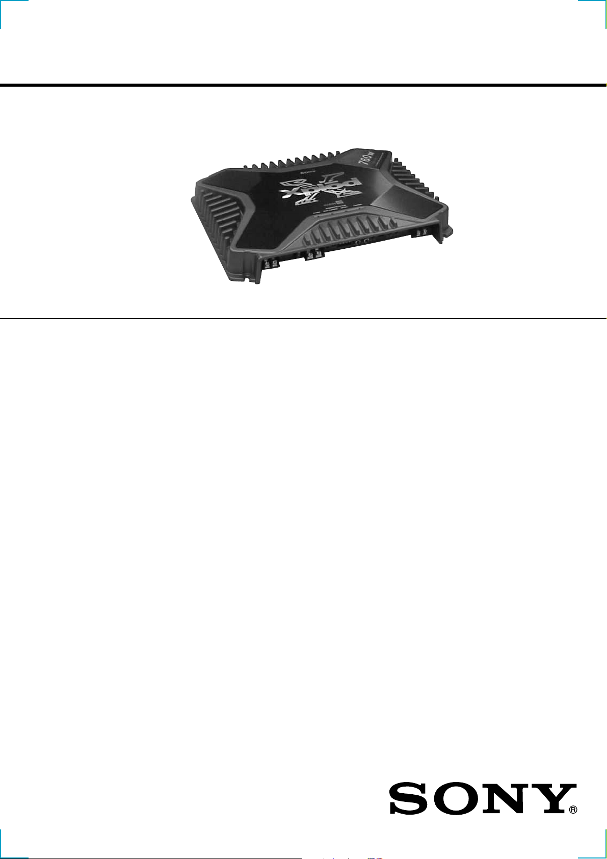
Photo: XM-1902GX
SPECIFICATIONS
AUDIO POWER SPECIFICATIONS
POWER OUTPUT AND TOTAL HARMONIC DISTORTION
150 watts per channel minimum continuous average power into
4 ohms, both channels driven from 20 Hz to 20 kHz with no more
than 0.04% total harmonic distortion per Car Audio Ad Hoc
Committee standards.
US Model
XM-1502SX/1902GX
Canadian Model
AEP Model
UK Model
E Model
XM-1502SX
Other Specifications
Circuit system OTL (output transformerless) circuit
Inputs RCA pin jacks
Outputs Speaker terminals
Speaker impedance 2 – 8 Ω (stereo) (XM-1502SX)
Maximum outputs 300 W × 2 (at 4 Ω)
Rated outputs (supply voltage at 14.4 V)
Frequency response 5 Hz – 100 kHz ( dB)
Harmonic distortion 0.005% or less (at 1 kHz, 4 Ω)
Input level adjustment range
Pulse power supply
High level input connector
Through out pin jacks
1.3 – 8 Ω (stereo) (XM-1902GX)
4 – 8 Ω (when used as a bridging amplifier)
760 W (monaural) at 4 Ω
150 W × 2 (20 Hz – 20 kHz, 0.04% THD,
at 4 Ω)
190 W × 2 (20 Hz – 20 kHz, 0.1% THD,
at 2 Ω)
190 W × 2 (20 Hz – 20 kHz, 0.1% THD,
at 1.3 Ω) (XM-1902GX)
380 W × 1 (20 Hz – 20 kHz, 0.1% THD,
at 4 Ω) (XM-1902GX)
380 W (monaural) (20 Hz – 20 kHz, 0.1% THD,
at 4 Ω) (XM-1502SX)
0.2 – 6.0 V (RCA pin jacks)
0.4 – 12.0 V (High level input)
+0.5
–3
High-pass filter 50 – 300 Hz, –12 dB/oct
Low-pass filter 50 – 300 Hz, –12 dB/oct
Low boost 0 – 10 dB (40 Hz)
Phase shift adjustment range (XM-1902GX)
Power supply voltage 10.5 – 16 V
Current drain at rated output : 40 A (at 4 Ω)
Dimensions Approx. 358 × 50 × 264 mm
Mass Approx. 3.5 kg (7 lb. 11 oz.) not incl. accessories
Supplied accessories Mounting screws (4)
Design and specifications are subject to change without
notice.
0° – 180° (at 40 Hz)
Remote input : 2 mA
1/8 × 2 1/4 × 10 1/2 in.)
(14
(w/h/d) not incl. projecting parts and controls
9-870-239-12
2001F0400-1
© 2001.6
STEREO POWER AMPLIFIER
Sony Corporation
e Vehicle Company
Shinagawa Tec Service Manual Production Group
1
Page 2

TABLE OF CONTENTS
1. GENERAL
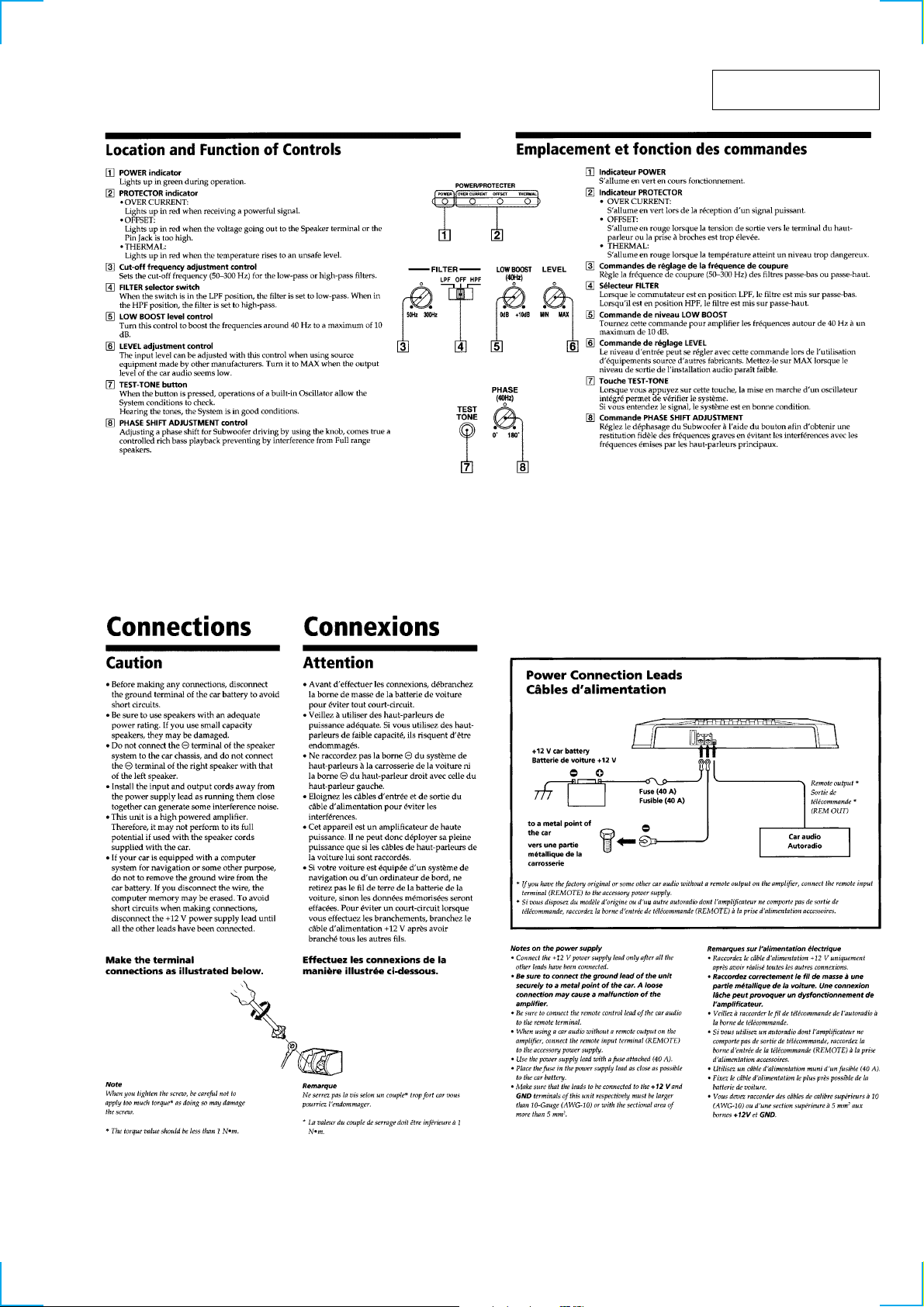
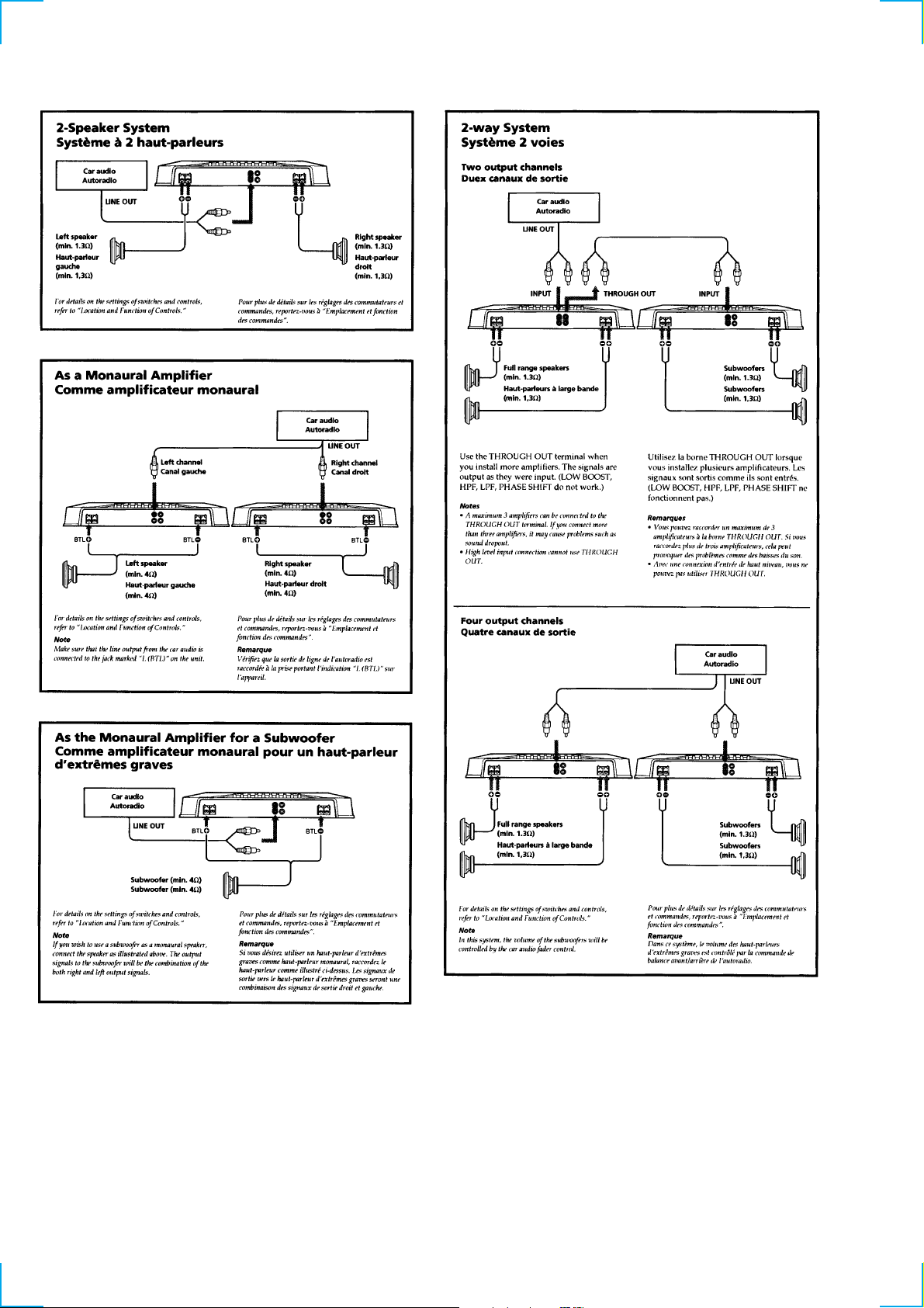
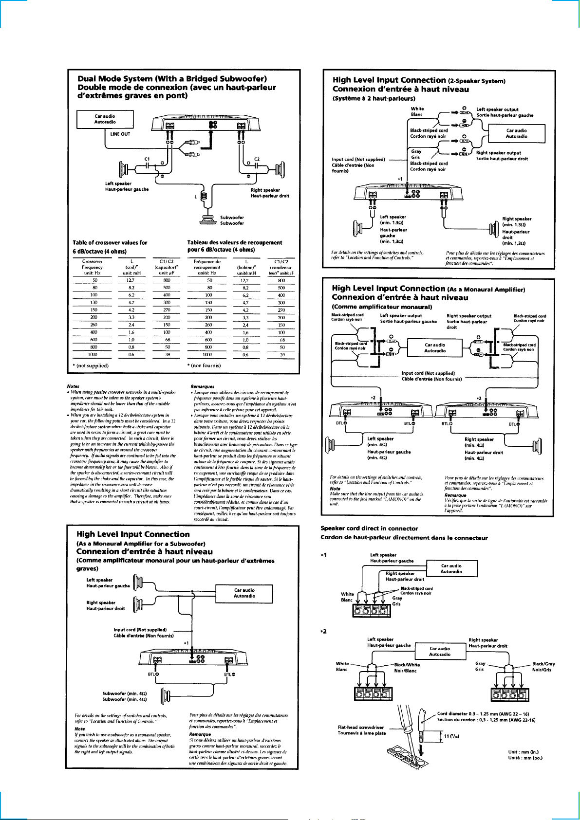
Location and Function of Controls.......................................... 3
Connections ............................................................................. 3
2. DISASSEMBLY
2-1. Plate, Bottom....................................................................... 6
2-2. Main Board ......................................................................... 6
2-3. Front Panel .......................................................................... 7
2-4. Led Board ............................................................................ 7
3. ELECTRICAL ADJUSTMENT...................................... 8
4. DIAGRAMS
4-1. Block Diagram .................................................................... 9
4-2. Printed Wiring Boards –Main Section– ............................ 11
4-3. Schematic Diagram –Main Section (1/2)– ........................ 12
4-4. Schematic Diagram –Main Section (2/2)– ........................ 13
5. EXPLODED VIEWS
5-1. Heat Sink Section .............................................................. 14
5-2. Main Board Section .......................................................... 14
6. ELECTRICAL PARTS LIST......................................... 15
Notes on Chip Component Replacement
• Never reuse a disconnected chip component.
• Notice that the minus side of a tantalum capacitor may be dam-
aged by heat.
2
Page 3
SECTION 1
GENERAL
This section is extracted
from instruction manual.
3
Page 4
456
Page 5
Page 6
SECTION 2
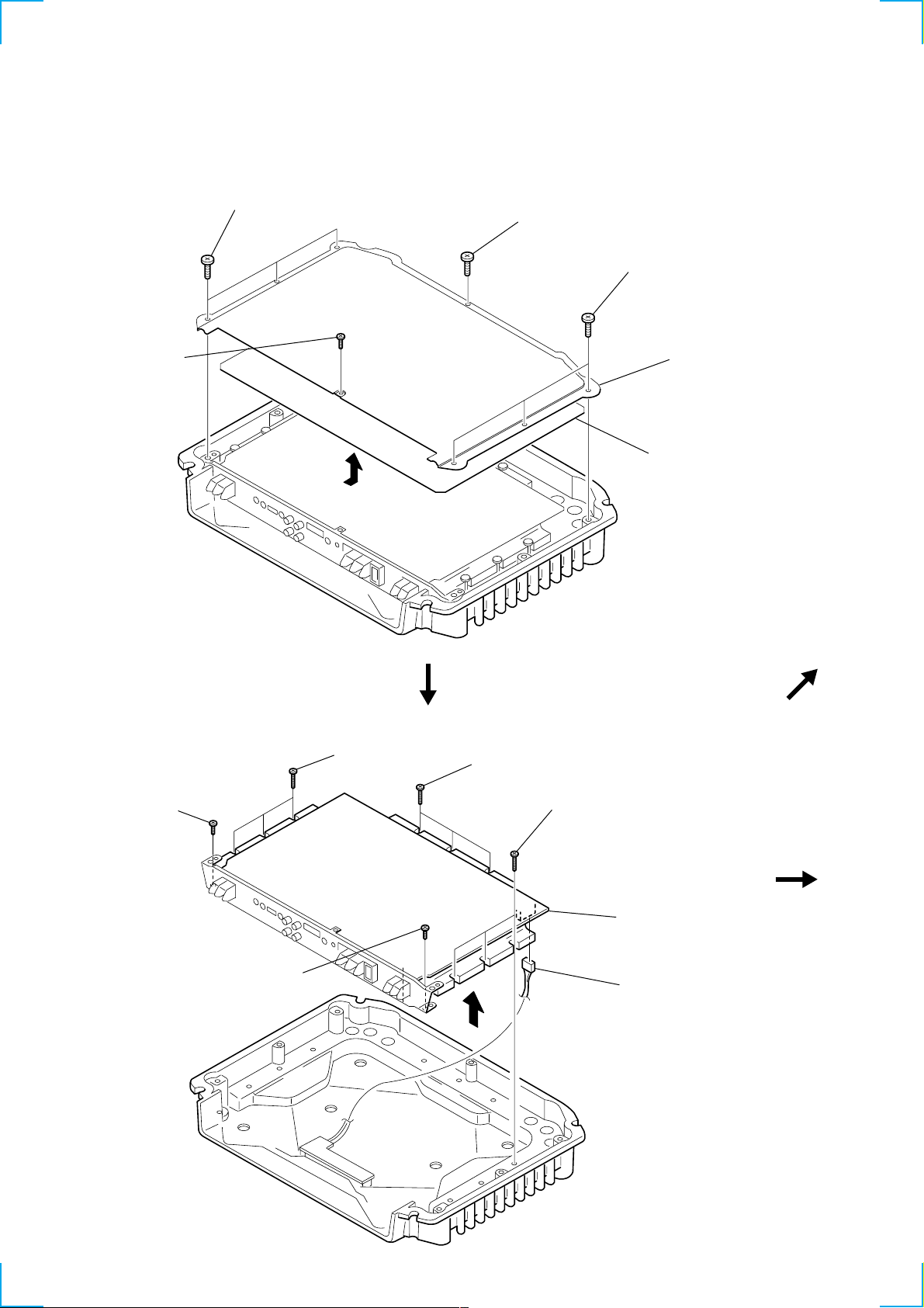
DISASSEMBLY
Note : Follow the disassembly procedure in the numerical order given.
2-1. PLATE, BOTTOM
4 P 2.6x2.8
3 BTP 3x6
6
2 BTP 3x6
1 BTP 3x6
5 plate, bottom
7 sheet, insulating
2-2. MAIN BOARD
2 BTP 3x6
1 BTP 3x6
3 B.TT. 3x14
4 B.TT. 3x14
5 B.TT. 3x14
7 MAIN board section
8 CN808
6
Page 7
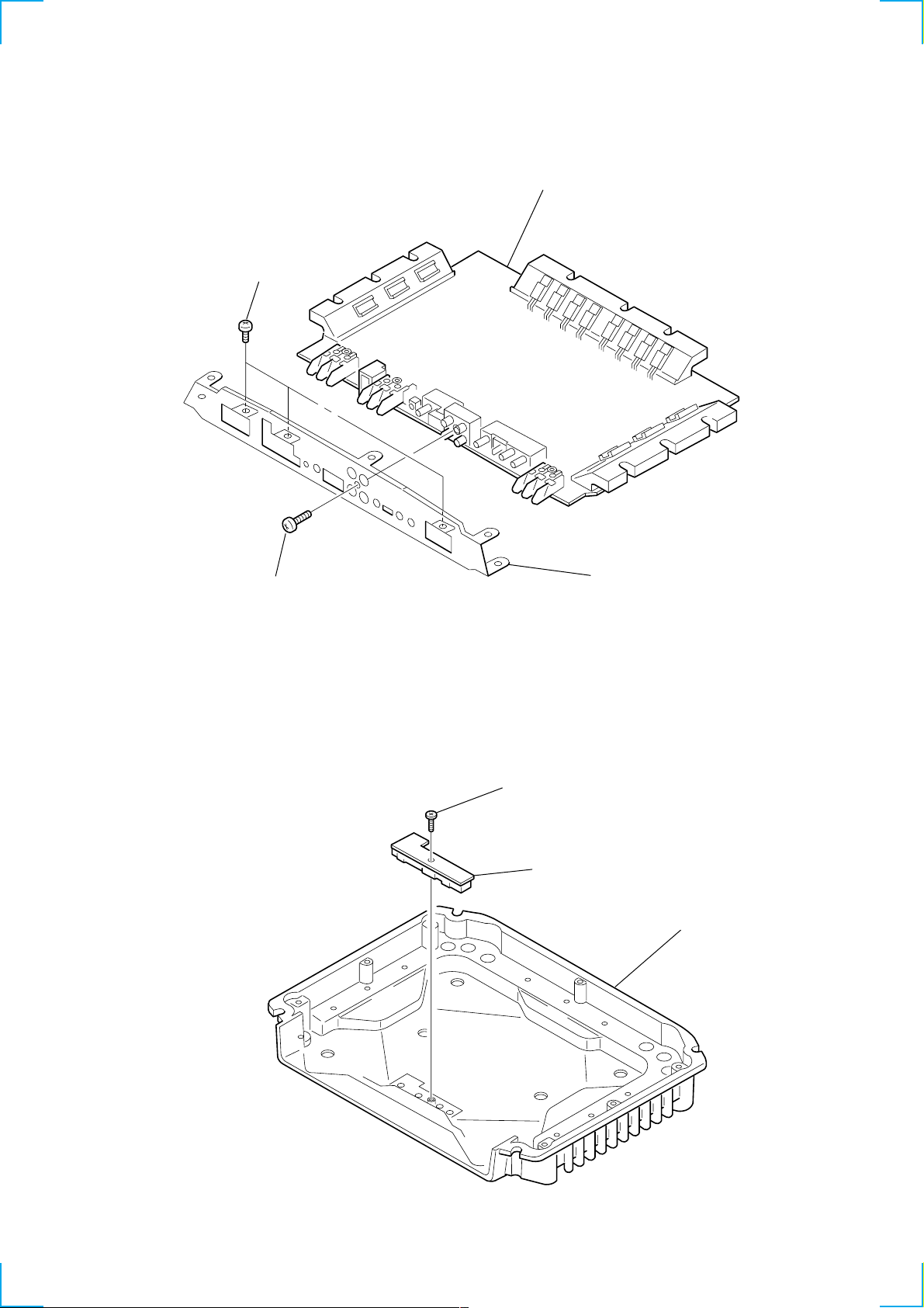
2-3. FRONT PANEL
)
4 MAIN board
2 P 3x8
2-4. LED BOARD
1 P 3x8
3 panel (2ch), front
1 BTP 3x6
2 LED board
heat sink (main
7
Page 8
l
Ver 1.1 2001.06
SECTION 3
ELECTRICAL ADJUSTMENT
Bias Adjustment
Note : In Bias Adjustment, adjust RV105 if any of Q108 through
Q113 are replaced. Adjust RV205 if any of Q208 through
Q213 are replaced.
Condition : This adjustment should be performed about one minute
after the remote mode is turned on at a room temperature of about 25°C.
Setting :
B+,REM terminal
set
Stabilized
Power suppy
Procedure :
1. Turn the variable resistors RV105 (L-CH) and RV205 (R-CH)
full clockwise as seen from the component side to minimize the
bias current.
2. The input signal is to be no signal.
3. Apply the voltage to the B+ and REM terminals from the stabilized power supply and gradually increase it up to 14.4 V while
checking for any unusual current.
4. For the XM-1502SX, adjust each of RV105 (L-CH) and RV205
(R-CH) so that the power current of the stabilized power supply
is increased in steps of 500 mA (total of 1 A). For the XM1902GX, adjust each of RV105 (L-CH) and RV205 (R-CH) so
that the power current is increased in steps of 600 mA (total of
1.2 A).
5. After adjustment, check that the power current is at 1.3 to 2.0 A.
GND termina
Adjustment Location : Main board (component side)
– MAIN BOARD (COMPONENT SIDE) –
RV105
BIAS ADJUSTMENT
RV205
BIAS ADJUSTMENT
8
Page 9

3
2
1
6
5
7 5 7 2 1 6 7
PRE AMP
IC101(1/2)
PRE AMP
IC101(2/2)
5
6
7
3
2
1
LOW BOOST
IC104(2/2)
LINE AMP
IC104(1/2)
H.L.F
IC102(2/2)
L.P.F
IC102(1/2)
L.P.F
IC103(2/2)
DIFFERENTIAL
AMP
Q103
POWER
AMP
Q108,110,112
OVER CURRENT
DET
Q114-116
DRIVE
AMP
Q105
DIFFERENTIAL
AMP
Q104
POWER
AMP
Q109,111,113
DRIVE
AMP
Q106
BIAS
Q107
LEVEL
SHIFT
Q101
LEVEL
FILTER
S801-1
LPF
OFF
HPF
LEVEL
RV103-1
LOW
BOOST
+14.2V
(B+)
-14.2V
(B–)
CNJ801-1
INPUT
RV101-1
FILTER
XM-1902GX
RV801-1
FILTER
RV801-2
FILTER
OUTPUT
(THROUGH)
OUTPUT
(THROUGH)
L
SPEAKER
OUT
L
SPEAKER
OUT
R
RV104-1
LINE
SWITCH
Q102
REM
12V
GND
2
3
10
4
1
6
5
7 5 7 2 1 2 1
PRE AMP
IC201(1/2)
PRE AMP
IC201(2/2)
5
6
7
3
2
1
LOW BOOST
IC204(1/2)
LINE AMP
IC204(2/2)
H.P.F
IC202(2/2)
L.P.F
IC202(1/2)
L.P.F
IC103(1/2)
DIFFERENTIAL
AMP
Q203
POWER
AMP
Q208,210,212
OVER CURRENT
DET
Q214-216
DRIVE
AMP
Q205
DIFFERENTIAL
AMP
Q204
POWER
ON/OFF
Q903
LINE SWITCH
CONTROL
Q801,802
POWER
AMP
Q209,211,213
DRIVE
AMP
Q206
BIAS
Q207
LEVEL
SHIFT
Q201
RV103-2
LOW
BOOST
+14.2V
(B+)
-14.2V
(B–)
CNJ801-2
CNJ803
INPUT
RV101-2
FILTER
RV801-3
FILTER
RV801-4
FILTER
R
L
HI LEVEL
INPUT
R
RV104-2
LINE
SWITCH
Q202
RV205
BIAS
RV105
BIAS
DC OFFSET
DET
Q803-805
15
16
1
2
14
12
B+
SWITCH
Q901,902
TEMP.DET
TH801
THP802,803
DC DET
IC901
REF.
REG
LED DRIVE
Q813
LED DRIVE
Q809
PROTECT LATCH
Q812
LED DRIVE
Q811
CN802
CN801
F901
DECT
D909
DECT
D905
DECT
D907
DECT
D906
DECT
D911,917
DECT
D908
DECT
D910
+53V
(B+)
+51V
(B+)
+53V
(B+)
-51V
(B–)
-51V
(B–)
-53V
(B–)
-14.2V
(B–)
-20.3V
(B–)
+14.2V
(B+)
+20.3V
(B+)
INVERTER
Q904,905
INVERTER
Q906,907
HI-CURRENT
/HI-VOLTAGE
DET
IC903,Q912
B+
REG
Q910
B+
REG
Q911
DRIVER
Q908
DRIVER
Q909
11
9
8
3
+14.2V
(B+)
+14.2V
(B+)
D811
THERMAL
D810
OFFSET
D809
OVER
CURRENT
D808
POWER
+20.3V
(B+)
-20.3V
(B–)
D922
D919
D920
D921
DECT
D912,918
DC-DC
CONVERTER
TRANSFORMER
T901
+14.2B
(B+)
-14.2B
(B–)
S301
TEST TONE
TEST TONE
GENERATOR
IC301(2/2)
TEST TONE
GENERATOR
IC301(1/2)
D301
D302
DC-DC CONVERTER
IC901
Q808
D808 D807
• Signal path
: AUDIO
CN804
CN805
1
2
1
2
04
1
2
1
PROTECT LATCH
Q810
XM-1902GX
FILTER
S801-2
LPF
OFF
HPF
(Q110,111,115:XM-1902GX)
(Q210,211,215:XM-1902GX)
XM-1502SX/1902GX
SECTION 4
DIAGRAMS
4-1. BLOCK DIAGRAM
99
Page 10

THIS NOTE IS COMMON FOR PRINTED WIRING BOARDS
AND SCHEMATIC DIAGRAMS.
(In addition to this, the necessary note is
printed in each block.)
for schematic diagram:
Note:
• All capacitors are in µF unless otherwise noted. pF: µµF
50 WV or less are not indicated except for electrolytics
and tantalums.
• All resistors are in Ω and 1/
specified.
4
W or less unless otherwise
• % : indicates tolerance.
• 2 : nonflammable resistor.
• U : B+ Line.
• V : B– Line.
• Power voltage is dc 14.4V and fed with regulated dc power
supply from +12V and REMOTE terminals.
• Voltage is dc with respect to ground under no-signal
condition.
• Voltages are taken with a VOM (Input impedance 10 MΩ).
Voltage variations may be noted due to normal production tolerances.
• Signal path.
F : AUDIO
for printed wiring boards:
Note:
• X : parts extracted from the component side.
• b : Pattern from the side which enables seeing.
(The other layer’s patterns are not indicated.)
• IC Block Diagram
IC901 µPC494GS
16 15 14 13 12 11 10 9
ERROR
ERROR
1 2 3 4 5 6 7 8
REF. REG.
0.1V
OSC
• Wavef orm
1V/DIV, 5µsec/DIV
1
3.4Vp-p
• Semiconductor Location (MAIN SECTION)
Ref. No. Location Ref. No. Location
D101 E-9
D102 E-9
IC902 F-9
IC903 A-10
D103 E-9
D104 E-9
D201 E-4
D202 E-3
D203 E-4
D204 E-4
D301 F-8
D302 G-7
D801 D-7
D802 D-7
D803 B-11
D804 D-12
D805 A-11
D806 D-1
D807 B-11
D820 C-12
D821 D-12
(D822) E-12
(D823) F-12
D824 F-12
D825 G-12
D826 C-1
D827 D-1
(D828) E-1
(D829) F-1
D830 F-1
D831 G-1
D901 G-10
D902 G-10
D905 A-4
D906 A-4
D907 A-9
D908 A-8
D909 D-5
D910 D-5
D911 D-6
D912 D-5
D913 B-2
D914 B-2
D915 B-3
D917 D-6
D918 D-5
D919 D-10
D920 D-10
D921 E-3
D922 E-3
Q101 F-4
Q102 E-7
Q103 F-9
Q104 F-9
Q105 E-10
Q106 E-10
Q107 G-11
Q108 C-11
Q109 D-11
(Q110) E-11
(Q111) F-11
Q112 F-11
Q113 G-11
Q114 C-12
(Q115) D-12
Q116 F-12
Q201 G-4
Q202 E-5
Q203 E-3
Q204 E-4
Q205 E-3
Q206 E-3
Q207 G-1
Q208 C-1
Q209 D-1
(Q210) E-1
(Q211) E-1
Q212 F-1
Q213 G-1
Q214 D-1
(Q215) D-1
Q216 F-1
Q801 D-7
Q802 D-7
Q803 B-1
Q804 B-1
Q805 B-1
Q809 A-11
Q810 A-12
Q811 A-11
Q812 B-11
Q813 B-11
Q901 F-10
Q902 F-10
Q903 G-10
Q904 A-8
IC101 F-6
IC102 F-5
IC103 F-5
IC104 F-3
IC201 F-6
IC202 G-5
IC204 G-3
IC301 F-8
Q905 A-7
Q906 A-5
Q907 A-6
Q908 A-7
Q909 A-6
Q910 B-2
Q911 B-2
Q912 B-3
IC901 B-10
( ) : XM-1902GX only
10 10
15µsec
IC901
5
Page 11

4-2. PRINTED WIRING BOARDS — MAIN SECTION — • Refer to page 10 for Semiconductor Location.
XM-1502SX/1902GX
Ver 1.1 2001.06
11 11
Page 12

XM-1502SX/1902GX
Ver 1.1 2001.06
4-3. SCHEMATIC DIAGRAM — MAIN SECTION (1/2) — • Refer to page 10 for IC Block Diagram. • Refer to page 10 for Waveform.
12 12
Page 13

4-4. SCHEMATIC DIAGRAM — MAIN SECTION (2/2) —
XM-1502SX/1902GX
Ver 1.1 2001.06
13 13
Page 14

NOTE:
51
52
53
54
54
63
63
56
56
55
54
56
55
57
58
59
59
59
61
62
63
61
60
#3
#3
55
54
56
55
63
1902GX
1502SX
1902GX
1502SX
• The mechanical parts with no reference
number in the exploded views are not supplied.
• Items marked “*” are not stocked since
they are seldom required for routine service.
Some delay should be anticipated
when ordering these items.
5-1. HEAT SINK SECTION
SECTION 5
EXPLODED VIEWS
• Color Indication of Appearance Parts
Example :
KNOB, BALANCE (WHITE) ... (RED)
RR
Parts Color Cabinet’s Color
1
8
2
• Accessories and packing materials and
hardware (# mark) list are given in
the last of this parts list.
5-2. MAIN BOARD SECTION
#1
F901
A
#1
7
7
B
7
6
#1
3
4
B
#1
A
5
#1
#2
#1
Ref. No. Part No. Description Remark Ref. No. Part No. Description Remark
1 3-225-070-01 PLATE (HEAT SINK), ORNAMENTAL (1902GX)
1 3-225-079-01 PLATE (HEAT SINK), ORNAMENTAL
1 3-225-079-41 PLATE (HEAT SINK), ORNAMENTAL
* 2 3-225-071-01 HEAT SINK (MAIN)
* 3 3-225-065-01 HOLDER, LED
(1502SX:US,CND)
(1502SX:AEP,UK,E)
* 4 1-681-206-11 LED BOARD
* 5 3-225-081-01 SHEET, INSULATING
* 6 3-225-068-01 PLATE, BOTTOM
7 3-225-185-01 SCREW (+B.TT.3X14)
8 3-225-153-01 SHEET (HIAT SINK), ADHESIVE
F901 1-533-743-11 FUSE (BLADE TYPE) (AUTO FUSE) 40A
Ref. No. Part No. Description Remark Ref. No. Part No. Description Remark
* 51 A-3326-762-A MAIN BOARD, COMPLETE (1502SX)
* 51 A-3326-764-A MAIN BOARD, COMPLETE (1902GX)
* 52 3-225-067-01 HEAT SINK (SUB 2)
53 3-225-183-01 SCREW (+PSW.TT.3XL)
* 54 3-225-080-01 HEAT SINK (RETAINER PLATE)
55 3-225-183-11 SCREW (+PSW.TT.3XL)
* 56 3-225-066-01 HEAT SINK (SUB 1)
* 57 3-225-063-01 BRACKET (2CH.VR1)
* 58 3-225-064-01 BRACKET (2CH.VR2)
59 3-225-184-01 SCREW (+PS.TT.3X6)
* 60 3-225-069-01 PANEL (2CH), FRONT (1902GX)
* 60 3-225-069-11 PANEL (2CH), FRONT (1502SX)
61 3-369-647-01 SCREW (M4 SPACER)
62 3-912-432-01 SCREW (B)
* 63 3-225-086-01 SHEET (TR), INSULATING
14 14
Page 15

Ver 1.1 2001.06
SECTION 6
ELECTRICAL PARTS LIST
NOTE:
• Due to standardization, replacements in
the parts list may be different from the
parts specified in the diagrams or the
components used on the set.
• RESISTORS
All resistors are in ohms.
METAL:Metal-film resistor.
METAL OXIDE: Metal oxide-film resistor.
F:nonflammable
Ref. No. Part No. Description Remark Ref. No. Part No. Description Remark
* 1-681-206-11 LED BOARD
**********
* 3-225-065-01 HOLDER, LED
< DIODE >
• Items marked “*” are not stocked since
they are seldom required for routine service.
Some delay should be anticipated
when ordering these items.
• SEMICONDUCTORS
In each case, u : µ, for example:
uA.. : µA.. uPA.. : µPA..
uPB.. : µPB.. uPC.. : µPC.. uPD.. : µPD..
• CAPACITORS
uF : µF
• COILS
uH : µH
C107 1-107-826-11 CERAMIC CHIP 0.1uF 10% 16V
C108 1-107-826-11 CERAMIC CHIP 0.1uF 10% 16V
C109 1-115-871-11 ELECT 1uF 20% 50V
C110 1-162-919-11 CERAMIC CHIP 22PF 5% 50V
C111 1-136-167-00 FILM 0.15uF 5% 50V
When indicating parts by reference
number, please include the board.
MAINLED
(1902GX)
D808 8-719-064-23 LED SEL2411G (POWER)
D809 8-719-302-91 LED SEL2111R (OVER CURRENT)
D810 8-719-302-91 LED SEL2111R (OFFSET)
D811 8-719-302-91 LED SEL2111R (THERMAL)
< TRANSISTOR >
Q808 8-729-230-49 TRANSISTOR 2SC2712-YG
< RESISTOR >
R812 1-216-041-00 METAL CHIP 470 5% 1/10W
R813 1-216-061-00 METAL CHIP 3.3K 5% 1/10W
R814 1-216-061-00 METAL CHIP 3.3K 5% 1/10W
R817 1-216-061-00 METAL CHIP 3.3K 5% 1/10W
R818 1-216-041-00 METAL CHIP 470 5% 1/10W
R819 1-216-073-00 METAL CHIP 10K 5% 1/10W
*************************************************************
* A-3326-762-A MAIN BOARD, COMPLETE (1502SX)
* A-3326-764-A MAIN BOARD, COMPLETE (1902GX)
*********************
* 3-225-063-01 BRACKET (2CH.VR1)
* 3-225-064-01 BRACKET (2CH.VR2)
* 3-225-066-01 HEAT SINK (SUB 1)
* 3-225-067-01 HEAT SINK (SUB 2)
* 3-225-080-01 HEAT SINK (RETAINER PLATE)
* 3-225-086-01 SHEET (TR), INSULATING
3-225-183-01 SCREW (+PSW.TT.3XL)
3-225-183-11 SCREW (+PSW.TT.3XL)
3-225-184-01 SCREW (+PS.TT.3X6)
7-685-646-79 SCREW +P 3X8 TYPE2 NON-SLIT
7-685-544-19 SCREW +BTP 3X5 TYPE2 N-S
< CAPACITOR >
C101 1-126-794-11 ELECT 4.7uF 20% 50V
C102 1-126-794-11 ELECT 4.7uF 20% 50V
C103 1-162-919-11 CERAMIC CHIP 22PF 5% 50V
C104 1-162-919-11 CERAMIC CHIP 22PF 5% 50V
C105 1-162-927-11 CERAMIC CHIP 100PF 5% 50V
C106 1-162-927-11 CERAMIC CHIP 100PF 5% 50V
C112 1-136-167-00 FILM 0.15uF 5% 50V
C113 1-126-794-11 ELECT 4.7uF 20% 50V
C114 1-126-794-11 ELECT 4.7uF 20% 50V
C115 1-126-794-11 ELECT 4.7uF 20% 50V
C116 1-162-923-11 CERAMIC CHIP 47PF 5% 50V
C117 1-126-794-11 ELECT 4.7uF 20% 50V
C118 1-127-715-11 CERAMIC CHIP 0.22uF 10% 16V
C119 1-126-796-11 ELECT 22uF 20% 35V
C120 1-162-927-11 CERAMIC CHIP 100PF 5% 50V
C123 1-126-786-11 ELECT 47uF 20% 16V
C124 1-107-826-11 CERAMIC CHIP 0.1uF 10% 16V
C126 1-162-925-11 CERAMIC CHIP 68PF 5% 50V
C127 1-107-826-11 CERAMIC CHIP 0.1uF 10% 16V
C128 1-136-161-00 FILM 0.047uF 5% 50V
C130 1-162-919-11 CERAMIC CHIP 22PF 5% 50V
C131 1-128-499-11 ELECT 220uF 20% 16V
C201 1-126-794-11 ELECT 4.7uF 20% 50V
C202 1-126-794-11 ELECT 4.7uF 20% 50V
C203 1-162-919-11 CERAMIC CHIP 22PF 5% 50V
C204 1-162-919-11 CERAMIC CHIP 22PF 5% 50V
C205 1-162-927-11 CERAMIC CHIP 100PF 5% 50V
C206 1-162-927-11 CERAMIC CHIP 100PF 5% 50V
C207 1-107-826-11 CERAMIC CHIP 0.1uF 10% 16V
C208 1-107-826-11 CERAMIC CHIP 0.1uF 10% 16V
C209 1-115-871-11 ELECT 1uF 20% 50V
(1902GX)
C210 1-162-919-11 CERAMIC CHIP 22PF 5% 50V
C211 1-136-167-00 FILM 0.15uF 5% 50V
C212 1-136-167-00 FILM 0.15uF 5% 50V
C213 1-126-794-11 ELECT 4.7uF 20% 50V
C214 1-126-794-11 ELECT 4.7uF 20% 50V
C215 1-126-794-11 ELECT 4.7uF 20% 50V
C216 1-162-923-11 CERAMIC CHIP 47PF 5% 50V
C217 1-126-794-11 ELECT 4.7uF 20% 50V
C218 1-127-715-11 CERAMIC CHIP 0.22uF 10% 16V
C219 1-126-796-11 ELECT 22uF 20% 35V
C220 1-162-927-11 CERAMIC CHIP 100PF 5% 50V
C221 1-107-826-11 CERAMIC CHIP 0.1uF 10% 16V
C222 1-162-927-11 CERAMIC CHIP 100PF 5% 50V
C223 1-126-786-11 ELECT 47uF 20% 16V
15
Page 16

MAIN
Ref. No. Part No. Description Remark Ref. No. Part No. Description Remark
C224 1-107-826-11 CERAMIC CHIP 0.1uF 10% 16V
C226 1-162-925-11 CERAMIC CHIP 68PF 5% 50V
C227 1-107-826-11 CERAMIC CHIP 0.1uF 10% 16V
C228 1-136-161-00 FILM 0.047uF 5% 50V
C230 1-162-919-11 CERAMIC CHIP 22PF 5% 50V
C937 1-128-126-11 ELECT 100uF 20% 25V
C938 1-128-576-11 ELECT 100uF 20% 63V
C939 1-128-576-11 ELECT 100uF 20% 63V
C940 1-162-964-11 CERAMIC CHIP 0.001uF 10% 50V
C941 1-162-964-11 CERAMIC CHIP 0.001uF 10% 50V
C231 1-107-826-11 CERAMIC CHIP 0.1uF 10% 16V
C301 1-162-970-11 CERAMIC CHIP 0.01uF 10% 25V
C302 1-162-970-11 CERAMIC CHIP 0.01uF 10% 25V
C303 1-162-970-11 CERAMIC CHIP 0.01uF 10% 25V
C304 1-162-970-11 CERAMIC CHIP 0.01uF 10% 25V
C305 1-107-826-11 CERAMIC CHIP 0.1uF 10% 16V
C801 1-126-796-11 ELECT 22uF 20% 35V
C802 1-162-964-11 CERAMIC CHIP 0.001uF 10% 50V
C803 1-126-786-11 ELECT 47uF 20% 16V
C804 1-115-339-11 CERAMIC CHIP 0.1uF 10% 50V
C805 1-162-964-11 CERAMIC CHIP 0.001uF 10% 50V
C806 1-126-796-11 ELECT 22uF 20% 35V
C807 1-162-962-11 CERAMIC CHIP 470PF 10% 50V
C808 1-162-962-11 CERAMIC CHIP 470PF 10% 50V
C809 1-126-794-11 ELECT 4.7uF 20% 50V
C810 1-162-964-11 CERAMIC CHIP 0.001uF 10% 50V
C901 1-115-339-11 CERAMIC CHIP 0.1uF 10% 50V
C902 1-115-339-11 CERAMIC CHIP 0.1uF 10% 50V
C903 1-162-964-11 CERAMIC CHIP 0.001uF 10% 50V
C904 1-162-964-11 CERAMIC CHIP 0.001uF 10% 50V
C909 1-130-471-00 MYLAR 0.001uF 5% 50V
C910 1-126-786-11 ELECT 47uF 20% 16V
C911 1-128-126-11 ELECT 100uF 20% 25V
C912 1-128-126-11 ELECT 100uF 20% 25V
C913 1-162-964-11 CERAMIC CHIP 0.001uF 10% 50V
C914 1-162-964-11 CERAMIC CHIP 0.001uF 10% 50V
C915 1-137-194-11 FILM 0.47uF 5% 50V
C916 1-136-161-00 FILM 0.047uF 5% 50V
C917 1-131-731-11 ELECT 2200uF 16V
C918 1-131-731-11 ELECT 2200uF 16V
C919 1-131-731-11 ELECT 2200uF 16V
C920 1-126-973-11 ELECT 2200uF 20% 50V
C921 1-126-973-11 ELECT 2200uF 20% 50V
C922 1-126-973-11 ELECT 2200uF 20% 50V
C923 1-126-973-11 ELECT 2200uF 20% 50V
C924 1-115-339-11 CERAMIC CHIP 0.1uF 10% 50V
C925 1-115-339-11 CERAMIC CHIP 0.1uF 10% 50V
C926 1-126-973-11 ELECT 2200uF 20% 50V
C927 1-126-973-11 ELECT 2200uF 20% 50V
C928 1-126-973-11 ELECT 2200uF 20% 50V
C929 1-126-973-11 ELECT 2200uF 20% 50V
C930 1-115-339-11 CERAMIC CHIP 0.1uF 10% 50V
C931 1-115-339-11 CERAMIC CHIP 0.1uF 10% 50V
C932 1-128-126-11 ELECT 100uF 20% 25V
C933 1-128-126-11 ELECT 100uF 20% 25V
C934 1-136-165-00 FILM 0.1uF 5% 50V
C935 1-136-165-00 FILM 0.1uF 5% 50V
C936 1-128-126-11 ELECT 100uF 20% 25V
C942 1-131-731-11 ELECT 2200uF 16V
C950 1-162-970-11 CERAMIC CHIP 0.01uF 10% 25V
< TERMINAL BOARD >
CN801 1-694-755-11 TERMINAL BOARD (2P+FUSE) (+12V, GND)
CN802 1-815-300-11 TERMINAL (1P) (REM)
CN804 1-694-754-11 TERMINAL BOARD (2P) (SPEAKER OUT L)
CN805 1-694-754-11 TERMINAL BOARD (2P) (SPEAKER OUT R)
< CONNECTOR >
CN803 1-794-219-11 CONNECTOR (4P) (HI LEVEL INPUT L/R)
CN806 1-506-987-11 PIN, CONNECTOR (PC BOARD) 5P
< JACK >
CNJ801 1-779-078-41 JACK, PIN 4P (INPUT L/R,
OUTPUT (THROUGH) L/R)
< DIODE >
D101 8-719-065-43 DIODE 02DZ15-Z(TPH3)
D102 8-719-065-43 DIODE 02DZ15-Z(TPH3)
D103 8-719-065-43 DIODE 02DZ15-Z(TPH3)
D104 8-719-065-43 DIODE 02DZ15-Z(TPH3)
D201 8-719-065-43 DIODE 02DZ15-Z(TPH3)
D202 8-719-065-43 DIODE 02DZ15-Z(TPH3)
D203 8-719-065-43 DIODE 02DZ15-Z(TPH3)
D204 8-719-065-43 DIODE 02DZ15-Z(TPH3)
D301 8-719-016-74 DIODE 1SS352
D302 8-719-016-74 DIODE 1SS352
D801 8-719-065-18 DIODE 02DZ6.8-Y(TPH3)
D802 8-719-016-74 DIODE 1SS352
D803 8-719-016-74 DIODE 1SS352
D804 8-719-016-74 DIODE 1SS352
D805 8-719-016-74 DIODE 1SS352
D806 8-719-016-74 DIODE 1SS352
D807 8-719-016-74 DIODE 1SS352
D820 8-719-016-74 DIODE 1SS352
D821 8-719-016-74 DIODE 1SS352
D822 8-719-016-74 DIODE 1SS352 (1902GX)
D823 8-719-016-74 DIODE 1SS352 (1902GX)
D824 8-719-016-74 DIODE 1SS352
D825 8-719-016-74 DIODE 1SS352
D826 8-719-016-74 DIODE 1SS352
D827 8-719-016-74 DIODE 1SS352
D828 8-719-016-74 DIODE 1SS352 (1902GX)
D829 8-719-016-74 DIODE 1SS352 (1902GX)
D830 8-719-016-74 DIODE 1SS352
D831 8-719-016-74 DIODE 1SS352
D901 8-719-065-18 DIODE 02DZ6.8-Y(TPH3)
16
Page 17

MAIN
Ref. No. Part No. Description Remark Ref. No. Part No. Description Remark
D902 8-719-065-46 DIODE 02DZ16-Z(TPH3)
D905 8-719-079-00 DIODE FCH10A15
D906 8-719-079-01 DIODE FRH10A15
D907 8-719-079-00 DIODE FCH10A15
D908 8-719-079-01 DIODE FRH10A15
JR118 1-216-295-11 SHORT 0
JR119 1-216-295-11 SHORT 0
JR120 1-216-295-11 SHORT 0
JR121 1-216-295-11 SHORT 0
JR122 1-216-295-11 SHORT 0
D909 8-719-054-55 DIODE 1SS306(TE85L)
D910 8-719-054-55 DIODE 1SS306(TE85L)
D911 8-719-053-18 DIODE 1SR154-400TE-25
D912 8-719-053-18 DIODE 1SR154-400TE-25
D913 8-719-065-43 DIODE 02DZ15-Z(TPH3)
D914 8-719-065-43 DIODE 02DZ15-Z(TPH3)
D915 8-719-065-18 DIODE 02DZ6.8-Y(TPH3)
D917 8-719-053-18 DIODE 1SR154-400TE-25
D918 8-719-053-18 DIODE 1SR154-400TE-25
D919 8-719-016-74 DIODE 1SS352
D920 8-719-016-74 DIODE 1SS352
D921 8-719-016-74 DIODE 1SS352
D922 8-719-016-74 DIODE 1SS352
< IC >
IC101 8-759-385-17 IC NJM4580E(TE2)
IC102 8-759-385-17 IC NJM4580E(TE2)
IC103 8-759-385-17 IC NJM4580E(TE2)
IC104 8-759-385-17 IC NJM4580E(TE2)
IC201 8-759-385-17 IC NJM4580E(TE2)
IC202 8-759-385-17 IC NJM4580E(TE2)
IC204 8-759-385-17 IC NJM4580E(TE2)
IC301 8-759-385-17 IC NJM4580E(TE2)
IC901 8-759-144-88 IC uPC494GS-T1
< PHOTO TRANSISTOR >
IC902 8-719-800-42 PHOTO TRANSISTOR TP521-1-A
IC903 8-719-800-42 PHOTO TRANSISTOR TP521-1-A
< JUMPER RESISTOR >
JR123 1-216-295-11 SHORT 0
JR124 1-216-295-11 SHORT 0
JR125 1-216-295-11 SHORT 0
JR126 1-216-295-11 SHORT 0
JR127 1-216-295-11 SHORT 0
JR128 1-216-295-11 SHORT 0
JR129 1-216-295-11 SHORT 0
JR130 1-216-295-11 SHORT 0
JR131 1-216-295-11 SHORT 0
JR132 1-216-295-11 SHORT 0
JR133 1-216-295-11 SHORT 0
JR134 1-216-295-11 SHORT 0
JR135 1-216-295-11 SHORT 0
JR136 1-216-295-11 SHORT 0
JR137 1-216-295-11 SHORT 0
JR138 1-216-295-11 SHORT 0
JR139 1-216-295-11 SHORT 0
JR140 1-216-295-11 SHORT 0
JR141 1-216-295-11 SHORT 0
JR142 1-216-295-11 SHORT 0
JR143 1-216-295-11 SHORT 0
JR144 1-216-295-11 SHORT 0
JR145 1-216-295-11 SHORT 0
JR146 1-216-295-11 SHORT 0
JR147 1-216-295-11 SHORT 0
JR148 1-216-295-11 SHORT 0
JR149 1-216-295-11 SHORT 0
JR200 1-216-296-00 SHORT 0
JR201 1-216-296-00 SHORT 0
JR202 1-216-296-00 SHORT 0
JR100 1-216-295-11 SHORT 0
JR101 1-216-295-11 SHORT 0
JR102 1-216-295-11 SHORT 0
JR103 1-216-295-11 SHORT 0
JR104 1-216-295-11 SHORT 0
JR105 1-216-295-11 SHORT 0
JR106 1-216-295-11 SHORT 0
JR107 1-216-295-11 SHORT 0
JR108 1-216-295-11 SHORT 0
JR109 1-216-295-11 SHORT 0
JR110 1-216-295-11 SHORT 0
JR111 1-216-295-11 SHORT 0
JR112 1-216-295-11 SHORT 0
JR113 1-216-295-11 SHORT 0
JR114 1-216-295-11 SHORT 0
JR115 1-216-295-11 SHORT 0
JR116 1-216-295-11 SHORT 0
JR117 1-216-295-11 SHORT 0
JR203 1-216-296-00 SHORT 0
JR204 1-216-296-00 SHORT 0
JR205 1-216-296-00 SHORT 0
JR206 1-216-296-00 SHORT 0
JR207 1-216-296-00 SHORT 0
JR208 1-216-296-00 SHORT 0
JR209 1-216-296-00 SHORT 0
JR210 1-216-296-00 SHORT 0
JR211 1-216-296-00 SHORT 0
JR212 1-216-296-00 SHORT 0
JR213 1-216-296-00 SHORT 0
JR214 1-216-296-00 SHORT 0
JR215 1-216-296-00 SHORT 0
JR216 1-216-296-00 SHORT 0
JR217 1-216-296-00 SHORT 0
JR218 1-216-296-00 SHORT 0
JR219 1-216-296-00 SHORT 0
JR220 1-216-296-00 SHORT 0
17
Page 18

Ver 1.1 2001.06
MAIN
Ref. No. Part No. Description Remark Ref. No. Part No. Description Remark
JR221 1-216-296-00 SHORT 0
JR222 1-216-296-00 SHORT 0
JR223 1-216-296-00 SHORT 0
JR224 1-216-296-00 SHORT 0
JR225 1-216-296-00 SHORT 0
JR226 1-216-296-00 SHORT 0
JR227 1-216-296-00 SHORT 0
JR228 1-216-296-00 SHORT 0
JR229 1-216-296-00 SHORT 0
JR230 1-216-296-00 SHORT 0
JR231 1-216-296-00 SHORT 0
JR232 1-216-296-00 SHORT 0
JR233 1-216-296-00 SHORT 0
JR234 1-216-296-00 SHORT 0
JR235 1-216-296-00 SHORT 0
JR236 1-216-296-00 SHORT 0
JR237 1-216-296-00 SHORT 0
JR238 1-216-296-00 SHORT 0
JR239 1-216-296-00 SHORT 0
JR240 1-216-296-00 SHORT 0
JR241 1-216-296-00 SHORT 0
JR242 1-216-296-00 SHORT 0
JR243 1-216-296-00 SHORT 0
JR244 1-216-296-00 SHORT 0
JR245 1-216-296-00 SHORT 0
JR246 1-216-296-00 SHORT 0
JR247 1-216-296-00 SHORT 0
JR248 1-216-296-00 SHORT 0
JR249 1-216-296-00 SHORT 0
JR250 1-216-296-00 SHORT 0
JR251 1-216-296-00 SHORT 0
JR252 1-216-296-00 SHORT 0
JR253 1-216-296-00 SHORT 0
JR254 1-216-296-00 SHORT 0
JR255 1-216-296-00 SHORT 0
JR256 1-216-296-00 SHORT 0
JR257 1-216-296-00 SHORT 0
JR258 1-216-296-00 SHORT 0
JR259 1-216-296-00 SHORT 0
JR260 1-216-296-00 SHORT 0
JR261 1-216-296-00 SHORT 0
JR262 1-216-296-00 SHORT 0
JR263 1-216-296-00 SHORT 0
JR264 1-216-296-00 SHORT 0
JR265 1-216-296-00 SHORT 0
< COIL >
Q101 8-729-230-49 TRANSISTOR 2SC2712-YG
Q102 8-729-202-38 TRANSISTOR 2SC3326N-A
Q103 8-729-014-86 TRANSISTOR 2SC4207-YGRTE85L
Q104 8-729-232-66 TRANSISTOR 2SA1618Y
Q105 8-729-207-89 TRANSISTOR 2SA1358-Y
Q106 8-729-207-82 TRANSISTOR 2SC3421-Y
Q107 8-729-055-13 TRANSISTOR 2SD1861-TV2
Q108 8-729-924-78 FET IRF540
Q109 8-729-053-85 FET IRF9540
Q110 8-729-924-78 FET IRF540 (1902GX)
Q111 8-729-053-85 FET IRF9540 (1902GX)
Q112 8-729-924-78 FET IRF540
Q113 8-729-053-85 FET IRF9540
Q114 8-729-230-49 TRANSISTOR 2SC2712-YG
Q115 8-729-230-49 TRANSISTOR 2SC2712-YG (1902GX)
Q116 8-729-230-49 TRANSISTOR 2SC2712-YG
Q201 8-729-230-49 TRANSISTOR 2SC2712-YG
Q202 8-729-202-38 TRANSISTOR 2SC3326N-A
Q203 8-729-014-86 TRANSISTOR 2SC4207-YGRTE85L
Q204 8-729-232-66 TRANSISTOR 2SA1618Y
Q205 8-729-207-89 TRANSISTOR 2SA1358-Y
Q206 8-729-207-82 TRANSISTOR 2SC3421-Y
Q207 8-729-055-13 TRANSISTOR 2SD1861-TV2
Q208 8-729-924-78 FET IRF540
Q209 8-729-053-85 FET IRF9540
Q210 8-729-924-78 FET IRF540 (1902GX)
Q211 8-729-053-85 FET IRF9540 (1902GX)
Q212 8-729-924-78 FET IRF540
Q213 8-729-053-85 FET IRF9540
Q214 8-729-230-49 TRANSISTOR 2SC2712-YG
Q215 8-729-230-49 TRANSISTOR 2SC2712-YG (1902GX)
Q216 8-729-230-49 TRANSISTOR 2SC2712-YG
Q801 8-729-216-22 TRANSISTOR 2SA1162-G
Q802 8-729-230-49 TRANSISTOR 2SC2712-YG
Q803 8-729-230-49 TRANSISTOR 2SC2712-YG
Q804 8-729-216-22 TRANSISTOR 2SA1162-G
Q805 8-729-230-49 TRANSISTOR 2SC2712-YG
Q809 8-729-230-49 TRANSISTOR 2SC2712-YG
Q810 8-729-230-49 TRANSISTOR 2SC2712-YG
Q811 8-729-216-22 TRANSISTOR 2SA1162-G
Q812 8-729-230-49 TRANSISTOR 2SC2712-YG
Q813 8-729-216-22 TRANSISTOR 2SA1162-G
Q901 8-729-106-60 TRANSISTOR 2SB1115A-YQ
Q902 8-729-216-22 TRANSISTOR 2SA1162-G
Q903 8-729-230-49 TRANSISTOR 2SC2712-YG
< TRANSISTOR >
L901 1-419-851-11 COIL, CHOKE 50uH
L902 1-410-396-41 INDUCTOR, FERRITE BEAD 0.45uH
< PILOT LAMP >
PL801 1-517-156-11 LAMP, PILOT (65mA/14V)
18
Q904 8-729-053-05 FET FKV550T
Q905 8-729-053-05 FET FKV550T
Q906 8-729-053-05 FET FKV550T
Q907 8-729-053-05 FET FKV550T
Q908 8-729-230-49 TRANSISTOR 2SC2712-YG
Q909 8-729-230-49 TRANSISTOR 2SC2712-YG
Page 19

MAIN
Ref. No. Part No. Description Remark Ref. No. Part No. Description Remark
Q910 8-729-207-82 TRANSISTOR 2SC3421-Y
Q911 8-729-207-89 TRANSISTOR 2SA1358-Y
Q912 8-729-230-49 TRANSISTOR 2SC2712-YG
< RESISTOR >
R101 1-216-837-11 METAL CHIP 22K 5% 1/16W
R102 1-216-837-11 METAL CHIP 22K 5% 1/16W
R103 1-216-837-11 METAL CHIP 22K 5% 1/16W
R104 1-216-837-11 METAL CHIP 22K 5% 1/16W
R105 1-208-494-61 RES-CHIP 2.2K 2% 1/8W
R106 1-216-845-11 METAL CHIP 100K 5% 1/16W
R107 1-216-845-11 METAL CHIP 100K 5% 1/16W
R108 1-216-025-11 RES-CHIP 100 5% 1/10W
(1902GX)
R109 1-216-833-11 METAL CHIP 10K 5% 1/16W
R110 1-216-833-11 METAL CHIP 10K 5% 1/16W
R111 1-216-833-11 METAL CHIP 10K 5% 1/16W
R112 1-216-837-11 METAL CHIP 22K 5% 1/16W
R113 1-216-833-11 METAL CHIP 10K 5% 1/16W
R114 1-216-833-11 METAL CHIP 10K 5% 1/16W
R115 1-216-827-11 METAL CHIP 3.3K 5% 1/16W
R116 1-216-831-11 METAL CHIP 6.8K 5% 1/16W
R117 1-216-827-11 METAL CHIP 3.3K 5% 1/16W
R118 1-216-845-11 METAL CHIP 100K 5% 1/16W
R119 1-216-845-11 METAL CHIP 100K 5% 1/16W
R120 1-216-845-11 METAL CHIP 100K 5% 1/16W
R147 1-220-894-11 METAL 0.22 10% 5W F
(1902GX)
R148 1-220-894-11 METAL 0.22 10% 5W F
(1902GX)
R149 1-220-894-11 METAL 0.22 10% 5W F
R150 1-216-825-11 METAL CHIP 2.2K 5% 1/16W
R151 1-216-821-11 METAL CHIP 1K 5% 1/16W
R152 1-215-859-00 METAL OXIDE 22 5% 1W F
R153 1-216-853-11 METAL CHIP 470K 5% 1/16W
R154 1-216-065-00 RES-CHIP 4.7K 5% 1/10W
R155 1-216-077-00 RES-CHIP 15K 5% 1/10W
R156 1-216-833-11 METAL CHIP 10K 5% 1/16W
R157 1-220-894-11 METAL 0.22 10% 5W F
R158 1-216-825-11 METAL CHIP 2.2K 5% 1/16W
R159 1-216-821-11 METAL CHIP 1K 5% 1/16W
R160 1-215-859-00 METAL OXIDE 22 5% 1W F
R161 1-216-017-00 RES-CHIP 47 5% 1/10W
(1902GX)
R162 1-216-017-00 RES-CHIP 47 5% 1/10W
(1902GX)
R163 1-216-825-11 METAL CHIP 2.2K 5% 1/16W
(1902GX)
R164 1-216-821-11 METAL CHIP 1K 5% 1/16W
(1902GX)
R165 1-216-833-11 METAL CHIP 10K 5% 1/16W
R166 1-216-833-11 METAL CHIP 10K 5% 1/16W
(1902GX)
R121 1-216-843-11 METAL CHIP 68K 5% 1/16W
R122 1-216-295-11 SHORT 0
R123 1-216-827-11 METAL CHIP 3.3K 5% 1/16W
R124 1-216-045-00 METAL CHIP 680 5% 1/10W
R125 1-216-837-11 METAL CHIP 22K 5% 1/16W
R126 1-216-829-11 METAL CHIP 4.7K 5% 1/16W
R127 1-216-833-11 METAL CHIP 10K 5% 1/16W
R128 1-216-811-11 METAL CHIP 150 5% 1/16W
R129 1-216-073-00 METAL CHIP 10K 5% 1/10W
R130 1-216-829-11 METAL CHIP 4.7K 5% 1/16W
R131 1-216-829-11 METAL CHIP 4.7K 5% 1/16W
R132 1-216-829-11 METAL CHIP 4.7K 5% 1/16W
R133 1-216-089-11 RES-CHIP 47K 5% 1/10W
R134 1-216-089-11 RES-CHIP 47K 5% 1/10W
R135 1-216-033-00 METAL CHIP 220 5% 1/10W
R136 1-216-839-11 METAL CHIP 33K 5% 1/16W
R137 1-216-833-11 METAL CHIP 10K 5% 1/16W
R138 1-216-033-00 METAL CHIP 220 5% 1/10W
R139 1-216-845-11 METAL CHIP 100K 5% 1/16W
R140 1-216-845-11 METAL CHIP 100K 5% 1/16W
R141 1-216-017-00 RES-CHIP 47 5% 1/10W
R142 1-216-017-00 RES-CHIP 47 5% 1/10W
R143 1-249-427-11 CARBON 6.8K 5% 1/4W
R144 1-249-421-11 CARBON 2.2K 5% 1/4W
R145 1-220-894-11 METAL 0.22 10% 5W F
R146 1-220-894-11 METAL 0.22 10% 5W F
R167 1-216-017-00 RES-CHIP 47 5% 1/10W
R168 1-216-017-00 RES-CHIP 47 5% 1/10W
R201 1-216-837-11 METAL CHIP 22K 5% 1/16W
R202 1-216-837-11 METAL CHIP 22K 5% 1/16W
R203 1-216-837-11 METAL CHIP 22K 5% 1/16W
R204 1-216-837-11 METAL CHIP 22K 5% 1/16W
R205 1-208-494-61 RES-CHIP 2.2K 2% 1/8W
R206 1-216-845-11 METAL CHIP 100K 5% 1/16W
R207 1-216-845-11 METAL CHIP 100K 5% 1/16W
R208 1-216-025-11 RES-CHIP 100 5% 1/10W
(1902GX)
R209 1-216-833-11 METAL CHIP 10K 5% 1/16W
R210 1-216-833-11 METAL CHIP 10K 5% 1/16W
R211 1-216-833-11 METAL CHIP 10K 5% 1/16W
R212 1-216-837-11 METAL CHIP 22K 5% 1/16W
R213 1-216-833-11 METAL CHIP 10K 5% 1/16W
R214 1-216-833-11 METAL CHIP 10K 5% 1/16W
R215 1-216-827-11 METAL CHIP 3.3K 5% 1/16W
R216 1-216-831-11 METAL CHIP 6.8K 5% 1/16W
R217 1-216-827-11 METAL CHIP 3.3K 5% 1/16W
R218 1-216-845-11 METAL CHIP 100K 5% 1/16W
R219 1-216-845-11 METAL CHIP 100K 5% 1/16W
R220 1-216-845-11 METAL CHIP 100K 5% 1/16W
R221 1-216-843-11 METAL CHIP 68K 5% 1/16W
R222 1-216-295-11 SHORT 0
R223 1-216-827-11 METAL CHIP 3.3K 5% 1/16W
R224 1-216-045-00 METAL CHIP 680 5% 1/10W
19
Page 20

MAIN
Ref. No. Part No. Description Remark Ref. No. Part No. Description Remark
R225 1-216-837-11 METAL CHIP 22K 5% 1/16W
R226 1-216-829-11 METAL CHIP 4.7K 5% 1/16W
R227 1-216-833-11 METAL CHIP 10K 5% 1/16W
R228 1-216-811-11 METAL CHIP 150 5% 1/16W
R229 1-216-073-00 METAL CHIP 10K 5% 1/10W
R304 1-216-833-11 METAL CHIP 10K 5% 1/16W
R305 1-216-833-11 METAL CHIP 10K 5% 1/16W
R306 1-216-833-11 METAL CHIP 10K 5% 1/16W
R307 1-216-833-11 METAL CHIP 10K 5% 1/16W
R308 1-216-829-11 METAL CHIP 4.7K 5% 1/16W
R230 1-216-829-11 METAL CHIP 4.7K 5% 1/16W
R231 1-216-829-11 METAL CHIP 4.7K 5% 1/16W
R232 1-216-829-11 METAL CHIP 4.7K 5% 1/16W
R233 1-216-089-11 RES-CHIP 47K 5% 1/10W
R234 1-216-089-11 RES-CHIP 47K 5% 1/10W
R235 1-216-033-00 METAL CHIP 220 5% 1/10W
R236 1-216-839-11 METAL CHIP 33K 5% 1/16W
R237 1-216-833-11 METAL CHIP 10K 5% 1/16W
R238 1-216-033-00 METAL CHIP 220 5% 1/10W
R239 1-216-845-11 METAL CHIP 100K 5% 1/16W
R240 1-216-845-11 METAL CHIP 100K 5% 1/16W
R241 1-216-017-00 RES-CHIP 47 5% 1/10W
R242 1-216-017-00 RES-CHIP 47 5% 1/10W
R243 1-249-427-11 CARBON 6.8K 5% 1/4W
R244 1-249-421-11 CARBON 2.2K 5% 1/4W
R245 1-220-894-11 METAL 0.22 10% 5W F
R246 1-220-894-11 METAL 0.22 10% 5W F
R247 1-220-894-11 METAL 0.22 10% 5W F
(1902GX)
R248 1-220-894-11 METAL 0.22 10% 5W F
(1902GX)
R249 1-220-894-11 METAL 0.22 10% 5W F
R250 1-216-825-11 METAL CHIP 2.2K 5% 1/16W
R251 1-216-821-11 METAL CHIP 1K 5% 1/16W
R252 1-215-859-00 METAL OXIDE 22 5% 1W F
R253 1-216-853-11 METAL CHIP 470K 5% 1/16W
R254 1-216-049-11 RES-CHIP 1K 5% 1/10W
R255 1-216-077-00 RES-CHIP 15K 5% 1/10W
R256 1-216-833-11 METAL CHIP 10K 5% 1/16W
R257 1-220-894-11 METAL 0.22 10% 5W F
R258 1-216-825-11 METAL CHIP 2.2K 5% 1/16W
R259 1-216-821-11 METAL CHIP 1K 5% 1/16W
R260 1-215-859-00 METAL OXIDE 22 5% 1W F
R261 1-216-017-00 RES-CHIP 47 5% 1/10W
(1902GX)
R262 1-216-017-00 RES-CHIP 47 5% 1/10W
(1902GX)
R263 1-216-825-11 METAL CHIP 2.2K 5% 1/16W
(1902GX)
R264 1-216-821-11 METAL CHIP 1K 5% 1/16W
(1902GX)
R265 1-216-833-11 METAL CHIP 10K 5% 1/16W
R266 1-216-833-11 METAL CHIP 10K 5% 1/16W
(1902GX)
R267 1-216-017-00 RES-CHIP 47 5% 1/10W
R268 1-216-017-00 RES-CHIP 47 5% 1/10W
R301 1-216-833-11 METAL CHIP 10K 5% 1/16W
R302 1-216-829-11 METAL CHIP 4.7K 5% 1/16W
R303 1-216-833-11 METAL CHIP 10K 5% 1/16W
R309 1-216-847-11 METAL CHIP 150K 5% 1/16W
R310 1-216-847-11 METAL CHIP 150K 5% 1/16W
R311 1-216-833-11 METAL CHIP 10K 5% 1/16W
R312 1-216-833-11 METAL CHIP 10K 5% 1/16W
R313 1-220-397-11 RES-CHIP 4.7M 5% 1/16W
R314 1-220-397-11 RES-CHIP 4.7M 5% 1/16W
R315 1-216-845-11 METAL CHIP 100K 5% 1/16W
R801 1-216-857-11 METAL CHIP 1M 5% 1/16W
R802 1-216-821-11 METAL CHIP 1K 5% 1/16W
R803 1-216-833-11 METAL CHIP 10K 5% 1/16W
R804 1-216-845-11 METAL CHIP 100K 5% 1/16W
R805 1-216-839-11 METAL CHIP 33K 5% 1/16W
R806 1-216-833-11 METAL CHIP 10K 5% 1/16W
R807 1-216-833-11 METAL CHIP 10K 5% 1/16W
R808 1-216-833-11 METAL CHIP 10K 5% 1/16W
R809 1-216-833-11 METAL CHIP 10K 5% 1/16W
R810 1-216-857-11 METAL CHIP 1M 5% 1/16W
R811 1-208-494-61 RES-CHIP 2.2K 2% 1/8W
R820 1-216-833-11 METAL CHIP 10K 5% 1/16W
R821 1-216-833-11 METAL CHIP 10K 5% 1/16W
R822 1-216-833-11 METAL CHIP 10K 5% 1/16W
R823 1-216-833-11 METAL CHIP 10K 5% 1/16W
R824 1-216-841-11 METAL CHIP 47K 5% 1/16W
R825 1-216-833-11 METAL CHIP 10K 5% 1/16W
R826 1-216-833-11 METAL CHIP 10K 5% 1/16W
R827 1-216-833-11 METAL CHIP 10K 5% 1/16W
R828 1-216-833-11 METAL CHIP 10K 5% 1/16W
R829 1-216-833-11 METAL CHIP 10K 5% 1/16W
R830 1-216-833-11 METAL CHIP 10K 5% 1/16W
R833 1-216-839-11 METAL CHIP 33K 5% 1/16W
R834 1-216-839-11 METAL CHIP 33K 5% 1/16W
R835 1-216-841-11 METAL CHIP 47K 5% 1/16W
R836 1-216-841-11 METAL CHIP 47K 5% 1/16W
R837 1-216-827-11 METAL CHIP 3.3K 5% 1/16W
R838 1-216-816-11 METAL CHIP 390 5% 1/16W
R839 1-216-857-11 METAL CHIP 1M 5% 1/16W
R840 1-216-816-11 METAL CHIP 390 5% 1/16W
R841 1-216-816-11 METAL CHIP 390 5% 1/16W
R842 1-216-816-11 METAL CHIP 390 5% 1/16W
(1902GX)
R843 1-216-816-11 METAL CHIP 390 5% 1/16W
(1902GX)
R844 1-216-816-11 METAL CHIP 390 5% 1/16W
R845 1-216-816-11 METAL CHIP 390 5% 1/16W
R846 1-216-816-11 METAL CHIP 390 5% 1/16W
R847 1-216-816-11 METAL CHIP 390 5% 1/16W
R848 1-216-816-11 METAL CHIP 390 5% 1/16W
(1902GX)
20
Page 21

MAIN
Ref. No. Part No. Description Remark Ref. No. Part No. Description Remark
R849 1-216-816-11 METAL CHIP 390 5% 1/16W
(1902GX)
R850 1-216-833-11 METAL CHIP 10K 5% 1/16W
R851 1-216-816-11 METAL CHIP 390 5% 1/16W
R852 1-216-816-11 METAL CHIP 390 5% 1/16W
R853 1-216-827-11 METAL CHIP 3.3K 5% 1/16W
R854 1-216-827-11 METAL CHIP 3.3K 5% 1/16W
R855 1-216-827-11 METAL CHIP 3.3K 5% 1/16W
(1902GX)
R856 1-216-827-11 METAL CHIP 3.3K 5% 1/16W
(1902GX)
R857 1-216-827-11 METAL CHIP 3.3K 5% 1/16W
R858 1-216-827-11 METAL CHIP 3.3K 5% 1/16W
R934 1-216-821-11 METAL CHIP 1K 5% 1/16W
R942 1-208-474-61 RES-CHIP 330 2% 1/8W
R943 1-208-474-61 RES-CHIP 330 2% 1/8W
< VARIABLE RESISTOR >
RV101 1-227-320-11 RES, VAR, CARBON 50KX2 (PHASE (40Hz))
(1902GX)
RV103 1-225-648-11 RES, VAR, CARBON 5KX2 (LOW BOOST)
RV104 1-225-648-11 RES, VAR, CARBON 5KX2 (LEVEL)
RV105 1-241-765-11 RES, ADJ, CERMET 22K
RV205 1-241-765-11 RES, ADJ, CERMET 22K
RV801 1-225-647-11 RES, VAR, CARBON 20KX4 (FILTER)
R859 1-216-827-11 METAL CHIP 3.3K 5% 1/16W
R860 1-216-827-11 METAL CHIP 3.3K 5% 1/16W
R861 1-216-827-11 METAL CHIP 3.3K 5% 1/16W
(1902GX)
R862 1-216-827-11 METAL CHIP 3.3K 5% 1/16W
(1902GX)
R863 1-216-827-11 METAL CHIP 3.3K 5% 1/16W
R864 1-216-827-11 METAL CHIP 3.3K 5% 1/16W
R901 1-216-833-11 METAL CHIP 10K 5% 1/16W
R902 1-216-827-11 METAL CHIP 3.3K 5% 1/16W
R903 1-216-837-11 METAL CHIP 22K 5% 1/16W
R904 1-216-835-11 METAL CHIP 15K 5% 1/16W
R905 1-216-848-11 METAL CHIP 180K 5% 1/16W
R906 1-216-065-00 RES-CHIP 4.7K 5% 1/10W
R907 1-216-190-00 RES-CHIP 470 2% 1/8W
R908 1-216-190-00 RES-CHIP 470 2% 1/8W
R909 1-216-061-00 METAL CHIP 3.3K 5% 1/10W
R910 1-216-073-00 METAL CHIP 10K 5% 1/10W
R911 1-216-073-00 METAL CHIP 10K 5% 1/10W
R912 1-208-474-61 RES-CHIP 330 2% 1/8W
R913 1-216-049-11 RES-CHIP 1K 5% 1/10W
R914 1-216-049-11 RES-CHIP 1K 5% 1/10W
R915 1-216-017-00 RES-CHIP 47 5% 1/10W
R916 1-216-001-00 METAL CHIP 10 5% 1/10W
R917 1-216-017-91 RES-CHIP 47 5% 1/10W
R918 1-208-474-61 RES-CHIP 330 2% 1/8W
R919 1-208-474-61 RES-CHIP 330 2% 1/8W
R920 1-216-001-00 METAL CHIP 10 5% 1/10W
R921 1-216-001-00 METAL CHIP 10 5% 1/10W
R922 1-216-001-00 METAL CHIP 10 5% 1/10W
R923 1-216-825-11 METAL CHIP 2.2K 5% 1/16W
R924 1-216-825-11 METAL CHIP 2.2K 5% 1/16W
< SWITCH >
S301 1-762-638-11 SWITCH, TACTILE (TEST TONE)
S801 1-572-185-11 SWITCH, SLIDE (FILTER)
< TRANSFORMER >
T901 1-435-857-11 TRANSFORMER, DC-DC CONVERTER
< THERMISTOR (POSITIVE) >
TH801 1-804-301-11 THERMISTOR (SMD)
TH802 1-804-301-11 THERMISTOR (SMD)
TH803 1-804-301-11 THERMISTOR (SMD)
TH804 1-804-301-11 THERMISTOR (SMD) (1902GX)
TH805 1-804-301-11 THERMISTOR (SMD) (1902GX)
TH806 1-804-301-11 THERMISTOR (SMD)
TH807 1-804-301-11 THERMISTOR (SMD)
TH808 1-804-301-11 THERMISTOR (SMD)
TH809 1-804-301-11 THERMISTOR (SMD)
TH810 1-804-301-11 THERMISTOR (SMD) (1902GX)
TH811 1-804-301-11 THERMISTOR (SMD) (1902GX)
TH812 1-804-301-11 THERMISTOR (SMD)
TH813 1-804-301-11 THERMISTOR (SMD)
THP802 1-810-326-11 THERMISTOR (CHIP TYPE)
THP803 1-810-326-11 THERMISTOR (CHIP TYPE)
*************************************************************
MISCELLANEOUS
***************
F901 1-533-743-11 FUSE (BLADE TYPE) (AUTO FUSE) 40A
*************************************************************
R925 1-216-081-00 METAL CHIP 22K 5% 1/10W
R926 1-216-081-00 METAL CHIP 22K 5% 1/10W
R927 1-216-833-11 METAL CHIP 10K 5% 1/16W
R928 1-216-073-00 METAL CHIP 10K 5% 1/10W
R929 1-216-033-00 METAL CHIP 220 5% 1/10W
R930 1-216-821-11 METAL CHIP 1K 5% 1/16W
R931 1-216-821-11 METAL CHIP 1K 5% 1/16W
R932 1-216-821-11 METAL CHIP 1K 5% 1/16W
R933 1-216-821-11 METAL CHIP 1K 5% 1/16W
21
Page 22

XM-1502SX/1902GX
Ref. No. Part No. Description Remark
ACCESSORIES & PACKING MATERIALS
********************************
3-228-684-11 MANUAL, INSTRUCTION (ENGLISH,FRENCH)
3-228-685-11 MANUAL, INSTRUCTION (ENGLISH,FRENCH)
3-228-685-21 MANUAL, INSTRUCTION (GERMAN,ITALIAN)
(1502SX:AEP,UK,E)
3-228-685-31 MANUAL, INSTRUCTION (SPANISH,
PORTUGUESE) (1502SX:AEP,UK,E)
3-228-685-41 MANUAL, INSTRUCTION (DUTCH,SWEDISH)
(1502SX:AEP,UK,E)
(1902GX)
(1502SX)
3-228-685-51 MANUAL, INSTRUCTION (GREEK,RUSSIAN)
3-228-685-61 MANUAL, INSTRUCTION (POLISH,
TRADITIONAL CHINESE) (1502SX:AEP,UK,E)
3-367-410-01 SCREW (DIA.5X15), TAPPING
*************************************************************
**************
HARDWARE LIST
**************
#1 7-685-545-14 SCREW +BTP 3X6 TYPE2 N-S
#2 7-627-556-07 SCREW, PRECISION +P 2.6X2.8
#3 7-685-646-79 SCREW +P 3X8 TYPE2 NON-SLIT
(1502SX:AEP,UK,E)
(MOUNTING SCREW)
22
Page 23

MEMO
XM-1502SX/1902GX
23
Page 24

XM-1502SX/1902GX
REVISION HISTORY
Clicking the version allows you to jump to the revised page.
Also, clicking the version at the upper right on the revised page allows you to jump to the next revised
page.
Ver. Date Description of Revision
1.1 2001. 06 Corrected error for Q108, 110, 112, 208, 210, 212 and R819.
Added for condition of Bias Adjustment. (SPM-01013)
1.0 2000. 12 New
(ENG-01006)
24
 Loading...