

Sony XL MP 40 H Service Manual
XL-MP40H
SERVICE MANUAL
No. S2518XLMP40H/
MICRO COMPONENT SYSTEM
(Except for U.K.)
CONTENTS
PRECAUTIONS FOR USING LEAD-FREE SOLDER
CHAPTER 1. GENERAL DESCRIPTION
[1] SAFETY PRECAUTION FOR SERVICE
MANUAL........................................................1-1
[2] IMPORT ANT SERVICE NOTES (FOR U.K.
ONLY)............................................................ 1-1
[3] SPECIFICATIONS .........................................1-2
[4] NAMES OF PARTS........................................ 1-3
CHAPTER 2. ADJUSTMENTS
[1] ADJUSTMENT...............................................2-1
[2] TEST MODE.................................................. 2-2
[3] When the CD does not function..................... 2-3
MODEL
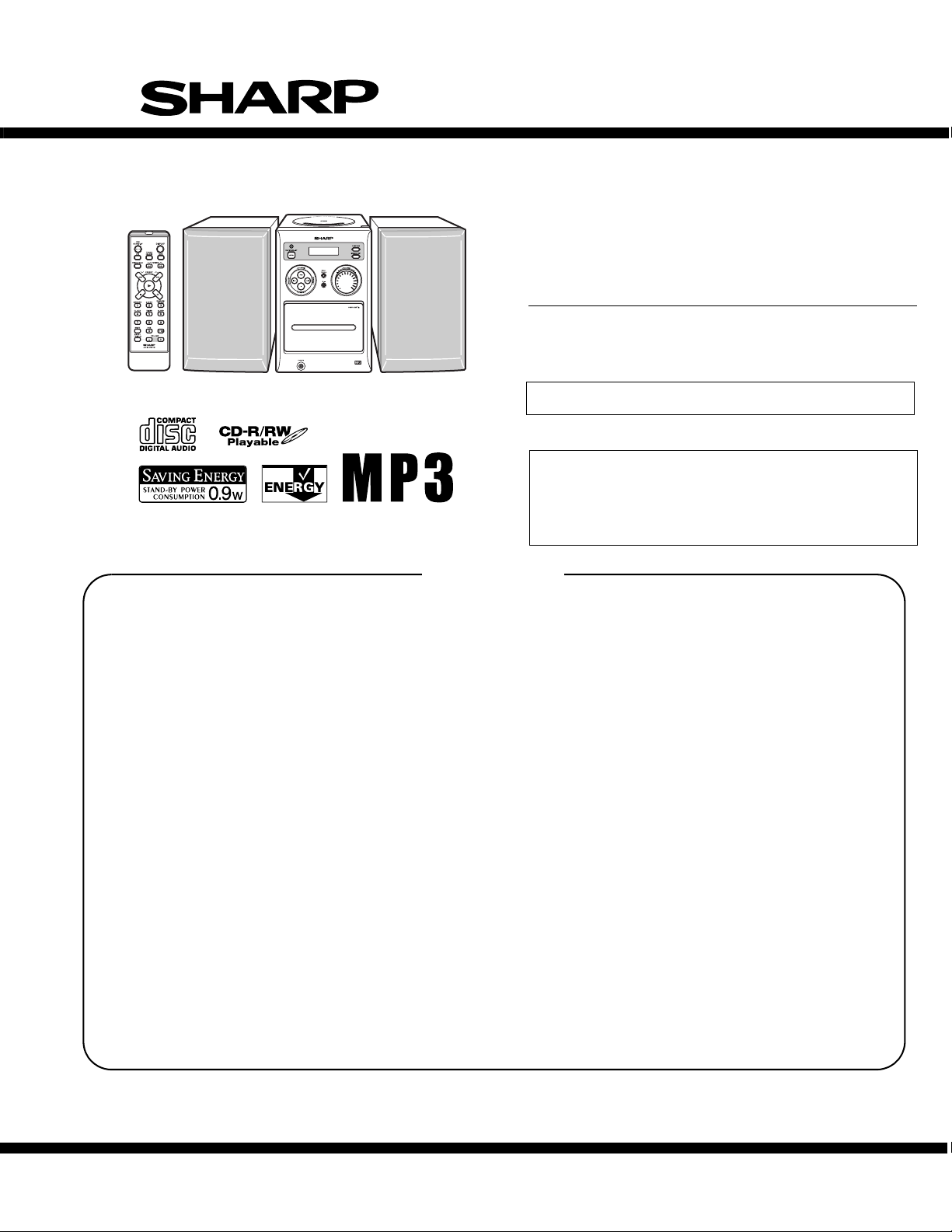
XL-MP40H Micro Component System consisting of XLMP40H (main unit) and CP-MP40H (speaker system).
• In the interests of user-safety the set should be restored to its original condition and only parts identical to those specified be used.
• Note for users in U.K.
Recording and playback of any material may require consent which
SHARP is unable to give. Please refer particularly to the provisions
of Copyright Act 1956, the Dramatic and Musical Performers Protection Act 1956, the Performers Protection Acts 1963 and 1972
and to any subsequent statutory enactments and orders.
CHAPTER 5. CIRCUIT DESCRIPTION
[1] WAVEFORMS OF CD CIRCUIT....................5-1
[2] VOLTAGE......................................................5-2
CHAPTER 6. CIRCUIT SCHEMATICS AND PARTS
LAYOUT
[1] NOTES ON SCHEMATIC DIAGRAM............ 6-1
[2] TYPES OF TRANSISTOR AND LED............6-1
[3] WIRING SIDE OF PWB/SCHEMATIC DIA-
GRAM............................................................6-2
CHAPTER 7. OTHERS
[1] FUNCTION TABLE OF IC.............................7-1
[2] LCD DISPLAY ...............................................7-6
XL-MP40H
CHAPTER 3. MECHANICAL DESCRIPTION
[1] REMOVING AND REINSTALLING THE
MAIN PARTS .................................................3-1
[2] DISASSEMBLY.............................................. 3-3
CHAPTER 4. DIAGRAMS
[1] BLOCK DIAGRAM......................................... 4-1
SHARP CORPORATION
Parts Guide
This document has been published to be used
for after sales service only.
The contents are subject to change without notice.
XL-MP40H
AudioXL-MP40HService ManualXLMP40HMarketE
PRECAUTIONS FOR USING LEAD-FREE SOLDER
1. Employing lead-free solder
"MAIN,DISPLAY,LED,POWER,SWITCH,JACK PWB," of this model employs lead-free solder. The LF symbol indicates
lead-free solder, and is attached on the PWB and service manuals. The alphabetical character following LF shows the
type of lead-free solder.
Example:
Indicates lead-free solder of tin, silver and copper.
2. Using lead-free wire solder
When fixingthe PWBsoldered with thelead-free solder,apply lead-free wire solder. Repairingwith conventionallead wire solder
may cause damage or accident due to cracks.
As the melting point of lead-free solder (Sn-Ag-Cu) is higher than the lead wire solder by 40 C, we recommend you to use a
dedicated soldering bit, ifyou are not familiar with how to obtain lead-free wire solder or soldering bit, contact our service station
or service branch in your area.
3. Soldering
As the melting point of lead-free solder (Sn-Ag-Cu) is about 220 C which is higher than the conventional lead solder by 40 C,
and as it has poor solder wettability, you may be apt to keep the soldering bit in contact with the PWB for extended period of
time. However, Since the land may be peeled off or the maximum heat-resistance temperature of parts may be exceeded,
remove the bit from the PWB as soon as you confirm the steady soldering condition.
Lead-free solder contains more tin, and the end of the soldering bit may be easily corrected. Make sure to turn on and off the
power of the bit as required.
If a different type of solder stays on the tip of the soldering bit, it is alloyed with lead-free solder. Clean the bit after e very use
of it.
When the tip of the soldering bit is blackened during use, file it with steel wool or fine sandpaper.
Be careful when replacing parts with polarity indication on the PWB silk.
Lead-free wire solder for servicing
Ref No. DescriptionParts No.
PWB-A1 MAINDCEKKV512SJ03
PWB-A2
PWB-A3
PWB-A4
PWB-A5
PWB-A6 DCEKKV512SJ03 SWITCH
DCEKKV512SJ03
DCEKKV512SJ03
DCEKKV512SJ03 JACK
DISPLAYDCEKKV512SJ03
POWER
LED
i
XL-MP40H
PROBE
AC
OUT
UNIT
SHORT-CIRCUIT
AC POWER
SUPPLY CORD
CONNECT THE PROBE
TO GND OF CHASSIS
SCREW
WITHSTANDING
VOLTAGE TESTER
AudioXL-MP40HService ManualXLMP40HMarketE
CHAPTER 1. GENERAL DESCRIPTION
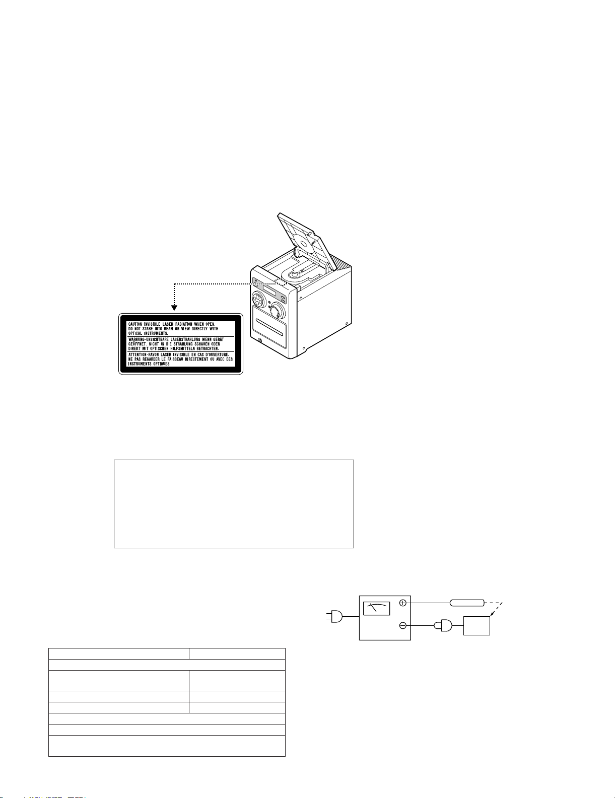
[1] SAFETY PRECAUTION FOR SERVICE MANUAL
Precaution to be taken when replacing and servicing the Laser Pickup.
The AEL (Accessible Emission Level) of Laser Power Output for this model is specified to be lower than Class 1 Requirements. However, the following precautions must be observed during servicing to protect your eyes against exposure to the Laser beam.
1) When the cabinet has been removed, the power is turned on without a compact disc, and th e Pickup is on a position out er than the lead-in position, the Laser will light for several seconds to detect a disc. Do not look into the Pickup Lens.
2) The Laser Power Output of the Pickup inside the unit and replacement service parts have already been adjusted prior to shipping.
3) No adjustment to the Laser Power should be attempted when replacing or servicing the Pickup.
4) Under no circumstances look directly into the Pickup Lens at any time.
5) C AUTION - Use of controls or adjustments, or performance of procedures other than those specified herein may result in hazardous radiation
exposure.
Laser Diode Properties
Material: GaAIAs
Wavelength: 780 nm
Emission Duration: continuous
Laser Output: max. 0.6 mW
[2] IMPORTANT SERVICE NOTES (FOR U.K.
ONLY)
Before returning the unit to the customer after completion of a repair or
adjustment it is necessary for the following withstand voltage test to be
applied to ensure the unit is safe for the customer to use.
Setting of Withstanding Voltage Tester and set.
ADVARSEL-USYNLIG LASERSTRÅLING VED ÅBNING. SE IKKE IND I
STRÅLEN-HELLER IKKE MED OPTISKE INSTRUMENTER.
VARO! AVATTAESSA OLET ALTTIINA NÄKYMÄTÖN LASERSÄTEILYLLE.
ÄLÄ TUIJOTA SÄTEESEEN ÄLÄKÄ KATSO SITÄ OPTISEN LAITTEEN
LÄPI.
VARNING-OSYNLIG LASERSTRÅLNING NÄR DENNA DEL ÄR ÖPPNAD.
STIRRA EJ IN I STRÅLEN OCH BETRAKTA EJ STRÅLEN GENOM
OPTISKT INSTRUMENT.
VAROITUS! LAITTEEN KÄYTTÄMINEN MUULLA KUIN TÄSSÄ
KÄYTTÖOHJEESSA MAINITULLA TAVALLA SAATTAA
ALTISTAA KÄYTTÄJÄN TURVALLISUUSLUOKAN 1
YLITTÄVÄLLE NÄKYMÄTTÖMÄLLE LASERSÄTEILYLLE.
VARNING - OM APPARATEN ANVÄNDS PÅ ANNAT SÄTT ÄN
I DENNA BRUKSANVISNING SPECIFICERAS. KAN
ANVÄNDAREN UTSÄTTAS FÖR OSYNLIG LASERSTRÅLNING, SOM ÖVERSKRIDER GRÄNSEN FÖR
LASERKLASS 1.
Set name set value
Withstanding Voltage Tester
Test voltage 4,240 VPEAK
Set time 6 secs
Set current (Cutoff current) 4 mA
Unit
Judgment
OK: The “GOOD” lamp lights.
NG: The “NG” lamp lights and the buzzer sounds.
3,000 VRMS
1 – 1
XL-MP40H
FOR A COMPLETE DESCRIPTION OF THE OPERATION OF THIS UNIT, PLEASE REFER
TO THE OPERATION MANUAL.
[3] SPECIFICATIONS
Except for U.K.
General
Power source AC 230 V, 50 Hz
Power
consumption
Dimensions Width: 160 mm (6-5/16")
Weight 2.5 kg (5.5 lbs.)
Power on: 25 W
Power stand-by: 0.9 W
Height: 240 mm (9-1/2")
Depth: 245 mm (10")
CD player
Type Compact disc player
Signal readout Non-contact, 3-beam semiconductor laser
D/A converter 1-bit D/A converter
Frequency
response
Dynamic range 90 dB (1 kHz)
pickup
20 - 20,000 Hz
Amplifier
Output power PMPO: 30 W (total)
MPO: 15 W (7.5 W + 7.5 W) (DIN 45 324)
RMS: 10 W (5 W + 5 W) (DIN 45 324)
Output terminals Speakers: 4 ohms
Headphones: 16 - 50 ohms
(recommended: 32 ohms)
Input terminals Video/Auxiliary (audio signal):
500 mV/47 k ohms
Tuner
Frequency range FM: 87.5 - 108.0 MHz
AM: 522 - 1,620 kHz
For U.K.
General
Power source AC 230 V - 240V, 50 Hz
Power
consumption
Dimensions Width: 160 mm (6-5/16")
Weight 2.5 kg (5.5 lbs.)
Power on: 25 W
Power stand-by: 0.9 W
Height: 240 mm (9-1/2")
Depth: 245 mm (10")
Cassette deck
Frequency
response
Signal/noise ratio 50 dB (recording/playback)
Wow and flutter 0.35 % (DIN 45 511)
50 - 14,000 Hz (normal tape)
Speaker
Type 10 cm (4") full-range speaker
Maximum input
power
Rated input power 5W
Impedance 4 ohms
Dimensions Width: 145 mm (5-3/4")
Weight 1.4 kg (3.1 lbs.)/each
10 W
Height: 240 mm (9-1/2")
Depth: 180 mm (7-1/16")
CD player
Type Compact disc player
Signal readout Non-contact, 3-beam semiconductor laser
D/A converter 1-bit D/A converter
Frequency
response
Dynamic range 90 dB (1 kHz)
pickup
20 - 20,000 Hz
Amplifier
Output power
Output terminals Speakers: 4 ohms
Input terminals Video/Auxiliary (audio signal):
RMS: 10 W (5 W + 5 W) (10 % T.H.D.)
Headphones: 16 - 50 ohms
(recommended: 32 ohms)
500 mV/47 k ohms
Tuner
Frequency range FM: 87.5 - 108.0 MHz
AM: 522 - 1,620 kHz
Specifications for this model are subject to change without prior
notice.
Cassette deck
Frequency
response
Signal/noise ratio 50 dB (recording/playback)
Wow and flutter 0.3 % (WRMS)
50 - 14,000 Hz (normal tape)
Speaker
Type 10 cm (4") full-range speaker
Maximum input
power
Rated input power 5W
Impedance 4 ohms
Dimensions Width: 145 mm (5-3/4")
Weight 1.4 kg (3.1 lbs.)/each
10 W
Height: 240 mm (9-1/2")
Depth: 180 mm (7-1/16")
1 – 2
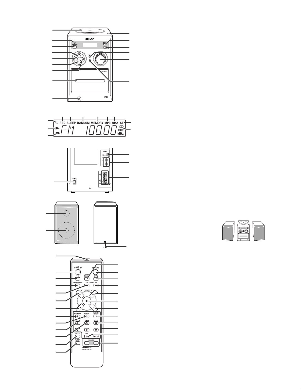
[4] NAMES OF PARTS
XL-MP40H
22
23
24
27
1
2
3
4
5
10
11
12
13
14
6
7
8
15
9
18 19 20 21
17
16
25
26
28
1.Disc Compartment
2.Remote Sensor
3.On/Stand-by Button
4.Disc Play or Pause, Tape Play,
Tuning Up Button
5.Disc Track Down or Fast Reverse, Tape Rewind,
Tuner Preset Down Button
6.Disc or Tape Stop, Tuning Down Button
7.Disc Track Up or Fast Forward, Tape Fast Forward,
Tuner Preset Up Button
8.Cassette Compartment
9.Headphone Socket
10.Disc Eject Button
11.Function Selector Button
12.Memory/Set Button
13.Bass/Treble Selector Button
14.Volume Control
15.Tape Record Pause Button
16.Tape Record Indicator
17.Sleep Indicator
18.Disc Random Play Indicator
19.Memory Indicator
20.MP3 Track Indicator
21.WMA Track Indicator
22.Timer Play Indicator
23.Disc Play Indicator
24.Disc Repeat Indicator
25.FM Stereo Mode Indicator
26.FM Stereo Receiving Indicator
29
27.AC Power Input Socket
28.FM/AM Loop Aerial Socket
30
29.Video/Auxiliary (Audio Signal) Input Sockets
30.Speaker Terminals
1.Bass Reflex Duct
2.Full-Range Speaker
3.Speaker Wire
1
2
3
4
17
5
6
7
8
9
10
11
12
13
14
15
18
19
20
21
22
23
24
25
26
27
28
16
Placing the speaker system:
The left and right speakers have
individual shapes. For best performance, place the speakers according to the illustration on the
right.
Note:
The speaker grilles are not removable.
4.Remote Control Transmitter
5.On/Stand-by Button
6.Disc Button
7.Video/Auxiliary Button
8.Disc Fast Reverse, Tuning Down Button
9.Disc Track Down, Tape Rewind, Tuner Preset Down,
Time Down Button
10.Disc or Tape Stop Button
11.Memory Button
12.Clear Button
13.Clock Button
14.Timer Button
15.Shift Button
16.Bass/Treble Selector Button
17.Tuner and Band Selector Button
18.MP3/WMA Display Button
19.Tape Button
20.Disc Fast Forward, Tuning Up Button
21.Disc Track Up, Tape Fast Forward, Tuner Preset Up,
Time Up Button
22.Disc or Tape Play Button
23.Disc Pause Button
24.Random/Repeat Button
25.Sleep Button
26.Direct Search Buttons
27.Tape Record Pause Button
28.Volume Up and Down Buttons
Right speakerLeft speaker
1 – 3
XL-MP40H
AM ANT.
FM OSC.
TP-VT=28Pin
28 2336
AM BAND
COVERAGE fL
FM RF
AM
Tracking
FM BAND
COVERAGE fL
MAIN PWB-A1
AM IF
AudioXL-MP40HService ManualXLMP40HMarketE
CHAPTER 2. ADJUSTMENTS
• FM Mute Level
Signal generator: 1 kHz, 40 kHz dev., FM modulated
[1] ADJUSTMENT
1. MECHANISM SECTION
• Driving Force Check
Torque Meter Specified Value
Play: TW-2412 Over 80 g
• Torque Check
Torque Meter Specified Value
Play: TW-2111 30 to 60 g.cm
Fast forward: TW-2231 55 to 140 g.cm
Rewind: TW-2231 55 to 140 g.cm
• Tape Speed
Test Tape Adjusting
Point
MTT-111 Variable Resis-
tor in motor.
TAPE MECHANISM
Specified Value Instrument
3,000 ± 30 Hz Headphone
M901
Tape
Motor
Connection
Terminal
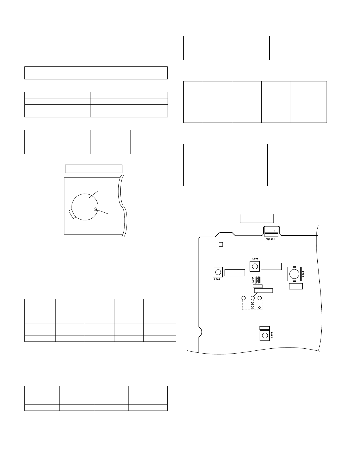
Frequency Display Adjusting
Parts
98.00 MHz
98.00 MHz - Input: CNP301
(30 dBµV)
Instrument
Connection
Output: Speaker Terminal
• FM Detection
Signal generator: 10.7 MHz FM sweep generator
Test
Stage
Frequency Frequency
Display
Setting/
Adjusting
Instrument
Connection
Parts
FM IF 10.7 MHz 98.00 MHz - Input: Pin 36 of
IC301
Output: Pin 23
of IC301
• FM RF
Signal generator: 1 kHz, 75 kHz dev., FM modulated
Test
Stage
Frequency Frequency
Display
Setting/
Adjusting
Instrument
Connection
Parts
FM Band
Coverage
FM RF 98.00 MHz
— 87.50 MHz (fL): L307
1.5 ± 0.1 V
98.00 MHz L304 *1
*1
(10 ~ 30dB)
*1. Input: Antenna Output: 23 Pin of IC301
Variable
resistor
in motor
Figure 1
2. TUNER SECTION
fL: Low-range frequency
fH: High-range frequency
• AM IF/RF
Signal generator: 400 Hz, 30%, AM modulated
Test Stage Frequency Frequency
Display
IF 450 kHz 1,602 kHz L305 *1
AM Band
— 522 kHz (fL): L306
Coverage
Setting/
Adjusting
Parts
1.1 ± 0.1 V
AM Tracking 990 kHz 990 kHz L302 *3
*1. Input: IC301 1Pin Output: IC301 23Pin
*2. Input: Input is not connected Output: TP-VT (IC301 28Pin)
*3. Input: Antenna Output:IC301 23Pin
• Check FM VT
Signal generator: 1 kHz, 40 kHz dev., FM modulated
Frequency Display Check Point Instrument
87.5 MHz 87.5 MHz 1.5V ± 1.0V TP-VT
108 MHz 108 MHz 5.0V ± 1.0V TP-VT
Instrument
Connection
*2
Connection
Figure 2 ADJUSTMENT POINTS
2 – 1
XL-MP40H
• Setting the Test Mode
Keeping the REW/REV button and BASS/TREBLE button pressed, turn on POWER. Then, the frequency is initially set in the memory as shown in
Table. Call it with the PRESET button to use it for adjustment and check of tuner circuit.
Preset No. BAND FM STEREO
1 FM STEREO FM 87.50 MHz
2 FM 108.00 MHz
3 FM 98.00 MHz
4 FM 90.00 MHz
5 FM 106.00 MHz
6 AM AM 522 kHz
7 AM 1620 kHz
8 AM 990 kHz
Preset No. BAND FM STEREO
9 AM AM 603 kHz
11~25 ——————
26 FM MONO FM 106.00 MHz
27 FM 90.00 MHz
28 FM 98.00 MHz
29 FM 108.00 MHz
30 FM 87.50 MHz
[2] TEST MODE
1. Turning on the test mode
Turning on the test mode
To tu rn on the specific test mode, press the ON/STAND-BY button, holding down the following two buttons in the or dinary stand-by mode (powe r off
state). In this case only the main unit button is valid. Even when the ON/STAND-BY of remote control button is set to on, the test mode is not turned
on.
[Ordinary test mode]
1. CD Test Mode(TEST 1) ........................FUNCTION + Tuning Down
2. Tuner Test Mode(TEST 2)......................FUNCTION + Preset Down
3. Volume Test Mode(TEST 3)....................FUNCTION + Tuning Up
4. Timer Test Mode(TEST 4) ......................FUNCT ION + Preset Up
5. Display Test Mode (TEST 5)...................FUNCTION + Bass/Treble
6. ALL KEY Test (TEST 6)....................MEMORY/SET + Tuning Up
7. Tuner clear test (TEST 7)................FUNCTION + Tape Rec
8. Soft reset test(TEST 8).....................MEMORY/SET + Preset Down
All test modes can be terminated by turning off the power with ON/STAND-BY key.
• CD test(TEST 1)
[cd step 1] Enter test mode.
↓ Hold down the “memory” button
[cd step 2] After some steps, the laser turns on.
↓ Hold down the “memory” button
[cd step 3] After some steps, focus search is performed.
↓ Hold down the “memory” button
[cd step 4] After some steps, CLV rotation is performed.
↓ Hold down the “memory” button
[cd step 5] CD playback starts.
↓ Hold down the “stop” button to return to [cd step 1] ––––––––––
←———————
A
A
In step 5, hold down the AUX key on the remote control. The tracking servo is switched on/off.
From step 3, the pick up can be moved with the FF/REW key.
• Tuner test (TEST 2)
CH BAND FREQUENCY
1 FM STEREO FM 87.50 MHz
2 FM 108.00 MHz
3 FM 98.00 MHz
4 FM 90.00 MHz
5 FM 106.00 MHz
6 AM AM 522 kHz
7 AM 1620 kHz
8 AM 990 kHz
9 AM 603 kHz
10 AM AM 1404 kHz
CH BAND FREQUENCY
11 ——————
·
·
35
36 FM MONO FM 106.00 MHz
37 FM 90.00 MHz
38 FM 98.00 MHz
39 FM 108.00 MHz
40 FM 87.50 MHz
2 – 2
XL-MP40H
• VOLUME test (TEST 3)
Starting from level 23 (default), check all the levels (0 - 23 - MAX).
• TIMER test(TEST4)
At 1:05, the power turns on to activate the tape function, and turns off after 90 seconds (equivalent to 90 minutes on the unit).
• Display test(TEST 5)
When test mode is activated, the entire display lights up. As the “PLAY” key is pressed, half of the display lights up alternately.
• ALL KEY test(TEST6)
In the test mode, hold down all the buttons on the main unit and then press the “ON/STAND-BY”button. “OK” appears.
If only the “ON/STAND-BY” button is pressed, “ERROR” appears.
• Tuner clear test (TEST 7)
All tuner preset stations are cleared.
• Soft reset test (TEST 8)
All data in RAM is cleared.
[3] When the CD does not function
The CD section may not operate when the objective lens of the optical pickup is dirty. Clean the objective lens, and check the playback operation.
When this section does not operate even after the above step is taken, check the following items.
Turn the power off.
Gently clean the lens with a lens cleaning tissue and a small amount of isopropyl alcohol.
Do not touch the lens with the bare hand.
Parts code
1. CD optical pickup Lens cleaner disc UDSKA0004AFZZ
HOW TO USE
1. Using the brush in the cleaner cap, apply 1 or 2 drops of the cleaning fluid to the brush on the CD cleaner disc which has
mark next to it.
the
2. Place the CD cleaner disc onto the CD disc tray with the brush side down, then press the play button.
3. You will hear music for about 20 seconds and the CD player will automatically stop. If it continues to turn, press the stop
button.
CAUTION
The CD lens cleaner should be effective for 30~50 operations, however if the brushes become worn out earller then please
replace the cleaner disc.
If the CD cleaner brushes become very wet then wipe off any excess fluid with a soft cloth.
Do not drink the cleaner fluid or allow it to come in contact with the eyes. In the event of this happening then drink and /
or rinse with clean water and seek medical advice.
The CD cleaner disc must not be used on car CD players or on computer CD ROM drives.
All rights reserved. Unauthorized duplicating, broadcasting and renting this product is prohibited by law.
Cleaner Liquid
Cleaning Disc
PARTS CODE: UDSKA0004AFZZ
2 – 3
AudioXL-MP40HService ManualXLMP40HMarketE
CHAPTER 3. MECHANICAL DESCRIPTION
[1] REMOVING AND REINSTALLING THE MAIN PARTS
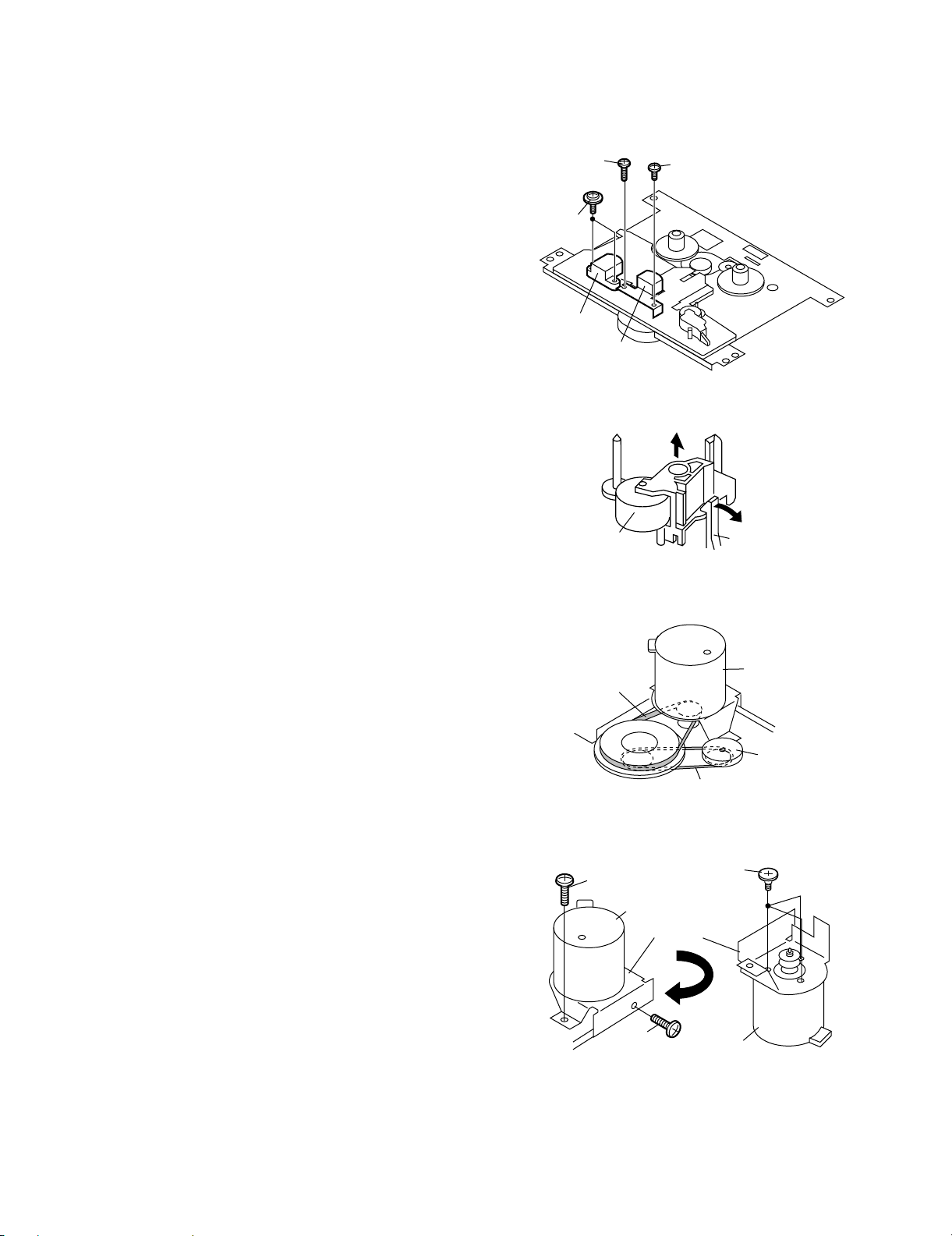
1. TAPE MECHANISM SECTION
Perform steps 1 to 5 and 8 of the disassembly method to remove the
tape mechanism. (See page 3-3.)
(A2)x1
ø2x7mm
XL-MP40H
(A2)x1
ø2x3mm
1.1. How to remove the record / playback and erase hea ds
(See Fig. 1)
1. Remove the screws (A1) x 2 pcs., to remove the erase head.
2. Remove the screws (A2) x 2 pcs., to remove the record/playback
head.
NOTE: After replacing the heads and performing the azimuth adjust-
ment, be sure to apply screwlock.
1.2. How to remove the pinch roller (See Fig. 2)
1. Carefully bend the pinch roller pawl in the direction of the arrow
<A>, and remove the pinch roller (B1) x 1 pc., upwards.
1.3. How to remove the belts (See Fig. 3)
1. Remove the main belt (C1) x 1 pc., from the motor pulley.
2. Remove the FF/REW belt (C2) x 1 pc., from the REW/FF roller.
3. Put on the belts in the reverse order of removal.
NOTE: When putting on the belt, ascertain that the belt is not twisted,
and clean it.
(A1)x2
ø2x8mm
Erase Head
Record/
Playback Head
Pinch Roller
(B1)x1
Main Belt
(C1)x1
Figure 1
<A>
Pinch Roller
Pawl
Figure 2
Motor
1.4. How to remove the motor (See Fig. 4)
1. Remove the main belt.
2. Remove the screws (D1) x 2 pcs., to remove the motor bracket.
3. Remove the screws (D2) x 3 pcs., to remove the motor.
NOTE: When mounting the motor, pay attention to the motor mounting
angle.
3 – 1
(D1)x1
ø2x4mm
Motor
(D1)x1
ø2x4mm
REW/FF
Clutch
FF/REW Belt
(C2)x1
Figure 3
(D2)x3
Special
Screw
Motor
Bracket
Motor
Figure 4
XL-MP40H
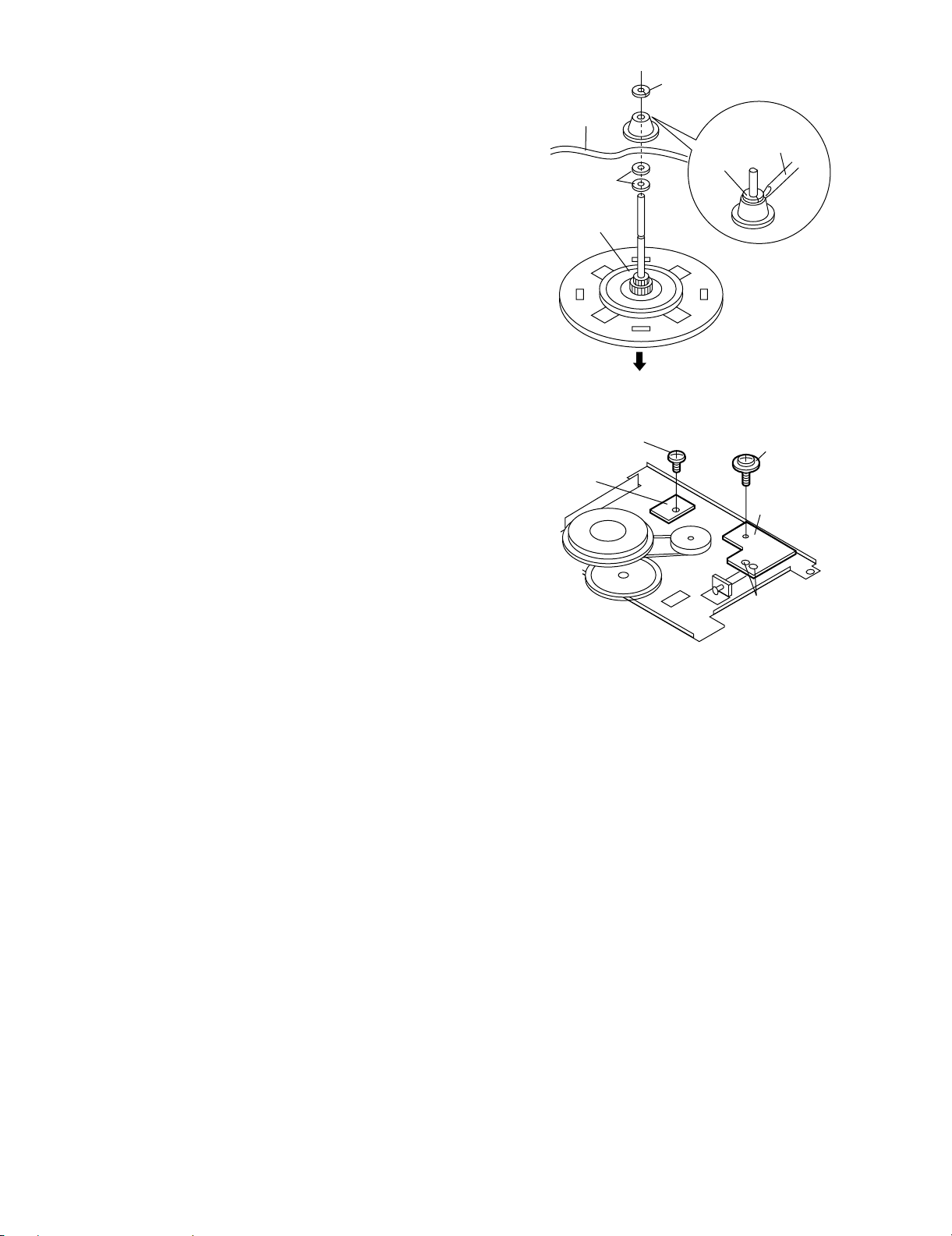
1.5. How to remove the flywheel (See Fig. 5)
1. Remove the belt.
2. Remove the stop washer (E1) x 1 pc., with a small precision screwdriver to extract the flywheel from the capstan metal.
NOTE: When the stop washer is deformed or damaged, replace it with
a new one.
1.6. How to reinstall the parts
Install each part in the reverse order of the removal with care.
Mechanism
Chassis
Washerx2
Flywheel
(E1)x1
Stop Washer
Stop
Washer
Figure 5
Driver
1.7. How to remove the tape mechanism PWB(See Fig. 6)
1. Remove the screw (F1) x 1 pc., to remove the tape mechanism
PWB.
2. Remove the screws (F2) x 1 pc.
3. Remove the solder joints (F3) x 2 pcs., to remove the tape mechanism PWB.
(F1)x1
ø2x3mm
Tape
Mechanism
PWB
(F2)x1
ø2x8mm
Tape
Mechanism
PWB
(F3)x2
Solder
Joint
Figure 6
3 – 2
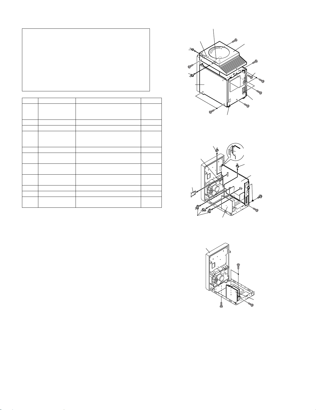
[2] DISASSEMBLY
Side Panel
(Right)
Rear Panel
(C1)x1
ø3x6mm
(C1)x1
ø3x10mm
Side Panel
(Lift)
(A1)x1
ø3x12mm
(A1)x2
ø3x12mm
(A1)x1
ø3x12mm
(A1)x1
ø3x10mm
(A2)x1
(B1)x2
ø3x12mm
(B1)x2
ø3x6mm
Top Cabinet
CD Mechanism PWB
(A2)x1
Open/Close
Switch PWB
Caution on Disassembly
Follow the below-mentioned notes when disassembling the unit and
reassembling it, to keep it safe and ensure excellent performance:
1) Take cassette tape and compact disc out of the unit.
2) Be sure to remove the power supply plug from the wall outlet
before starting to disassemble the unit.
3) Take off nylon bands or wire holders where they need to be
removed when disassembling the unit. After servicing the unit,
be sure to rearrange the leads where they were before disassembling.
4) Take sufficient care on static electricity of integrated circuits and
other circuits when servicing.
STEP REMOVAL PROCEDURE FIGURE
1 Top Cabinet 1. Screw...........................(A1) x 5
2. Socket
3. Flat cable.....................(A3) x 1
2 Side Panel 1. Screw...........................(B1) x 4 1
3 Rear Panel 1. Screw..........................(C1) x 2 1
4 Main PWB 1. Screw..........................(D1) x 3
2. Socket.........................(D2) x 5
3. Socket.........................(D3) x 1
5 Front Panel 1. Screw...........................(E1) x 1 3
6 Power PWB 1. Screw...........................(F1) x 1
2. Screw...........................(F2) x 2
7 Display PWB 1. Knob............................(G1) x 1
2. Screw..........................(G2) x 8
8 Tape Mechanism 1. Open the cassette holder
2. Screw..........................(H1) x 4
9 Jack PWB 1. Screw...........................(J1) x 1 4
10 Switch PWB 1. Screw...........................(K1) x 1 5
11 CD Mechanism
(Note)
Note :
After removing the connector for the optical pickup from the connector,
wrap the conductive aluminium foil around the front end of the connector so as to protect the optical pickup from electrostatic damage.
1. Screw...........................(L1) x 4 5
..........................
(A2) x 2
XL-MP40H
1
2
(D2)x1
Power PWB
Figure 1
(D3)x1
(D2)x1
Main PWB
(D1)x2
ø3x12mm
(D1)x1
ø3x6mm
Figure 2
2
Tape
3
4
4
Mechanism
PWB
(A3)x1
(D2)x3
3 – 3
Front Panel
(E1)x1
ø3x6mm
Figure 3
(F2)x2
ø3x8mm
Power
PWB
(F1)x1
ø3x6mm
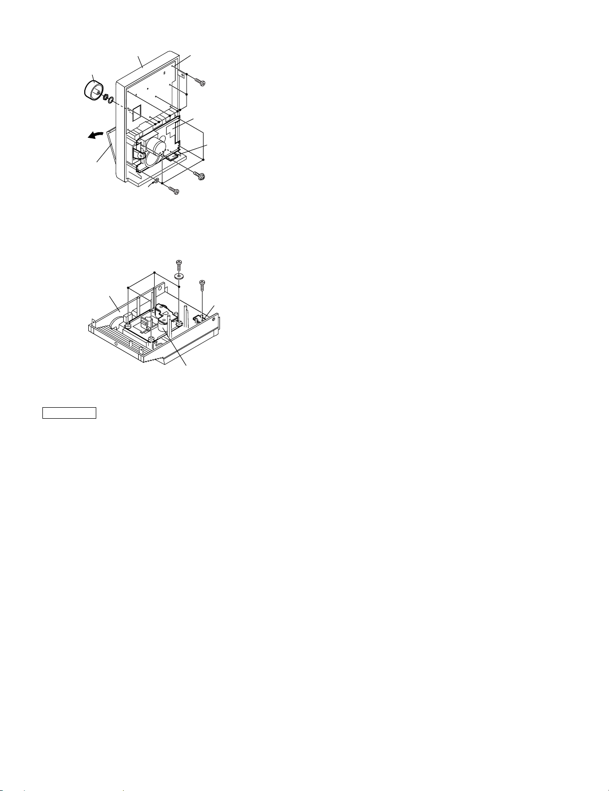
XL-MP40H
Front Panel
(G1)x1
Open
Cassette
Holder
Top Cabinet
Display PWB
(G2)x8
ø2.5x10mm
Tape
Mechanism
Jack PWB
(J1)x1
ø2.5x10mm
(H1)x4
ø2.5x10mm
Figure 4
(L1)x4
ø2.5x10mm
(K1)x1
ø2.5x10mm
Switch PWB
CD Mechanism
Figure 5
CP-MP40H
These speaker CP-MP40H are available in assembles only and may
not be disassembled.
3 – 4

-MEMO-
XL-MP40H
3 – 5
XL-MP40H
1
2
3
4
5
6
O
Y
6
AudioXL-MP40HService ManualXLMP40HMarketE
CHAPTER 4. DIAGRAMS
[1] BLOCK DIAGRAM
AM LOOP
ANTENNA
FM ANTENNA
HEADPHONES
LF651
LINE
FILTER
1
1
2
2
3
3
+
L-CH
-
SO601
SPEAKER
TERMINAL
-
R-CH
+
JK101
F101
T200mA L 250V
AC POWER
SUPPLY CORD
Except for U.K.: AC 230 V, 50 Hz
U.K.: AC 230-240 V, 50 Hz
CNP301
POWER
TRANSFORMER
FM IF
CF301
T601
AM
Tracking
BAND PASS
FILTER
BF301
CNP602
1
2
3
4
5
Q303
AM ANT.
CNS602
1
2
3
4
5
L302
(L)
(R)
1
2
3
4
5
6
CNW602
CF303
RP601
RP602
D305
+B
FM IF
IC101
LA4631++
POWER AMP.
D102
D101
D103
D104
D659
D658
AM OSC
D306
L304
FM RF
33 32 31
VCC2
GND2
FMRF-OUT
FM-OSC
REG
Q104
+B
FM-MIX
GND1
-B
AM-MIX
CF304
Q664
AM-OSC
VCC1
FMRF-IN
AMRF-IN
123 1817164 5 6 7 8 9 10 11 12 13 14 15
L305
AM IF
D656
D657
AM BAND
COVERAGE fL
L306
3
2
1
D307
L307
FM OSC
B02
B01
AMIFIN
FMIFIN
AM IF
123457612 10 9 81113
Q665
Q661
Q302
LP-IN
LP-OUT
P-CCMP
P-DET
POW_STB
Q613
4
5
6
PD
FM-DET
CF302
AGC
L-OUT
FM IF
Q662
AMLOWOUT
R-OUT
Q612
Q611
TP-VT
222324252627282930
DET-OUT
VSS
Q660
VTCC
X301
75KHz
19202136 35 34
VDD
XOUT
MPX-IN
CL
DI
CE
31
31
P_CON
Q658
CONSTANT
VOLTAGE
Q301
XIN
IC301
D0
LV23002M
FM FRONT END
IC680
AN78L05
CONSTANT
VOLTAGE
REGULATOR
+5V
2
2
IC681
AN78L05
CONSTANT
VOLTAGE
REGULATOR
PLL(TUNER)
FM IF DET./FMMPX./AM IF
CNP704
VP
-B
CD PICKUP UNIT
FOTR-
TR+
FO+
ACTUATOR
VR
MD
LD
F
C
B
A
D
E
CD MECHANISM UNIT (222)
MECHANISM PWB
SPINDLE
MOTOR
SLED
MOTOR
PICKUP IN
TO DISPLAY PWB
654321
VP
+5V
CD+B
P_CON
P_MUTE
POW_STB
TAPE MECHANISM ASS'Y
(221)
ERASE HEAD
RECORD/PLAYBACK
HEAD
SOL901
SOLENOID
-
M
+
M901
TAPE
MOTOR
+
M
-
+
M
-
L-CH
R-CH
SW902
PLAY
SW901
FOOL
470
PHOTO
INTERRUPTER
PLSN
TR+
FO+
GND
VCC
FOTR-
MD
VR
LD
F
C
B
A
D
E
VC
Q
PLA
FO
Figure 4-1 BLOCK DIAGRAM (1/3)
4 – 1
UNIT (222)
B
+
-
+
-
B
ISM ASS'Y
D
CK
02
Y
01
L
470
PLSN
O
RUPTER
FO-
TRTR+
FO+
MD
VR
LD
GND
F
C
B
A
D
E
VCC
VC
PLAY SW
FOOL SW
XL-MP40H
+B
16
15
14
13
12
11
10
9
8
7
6
5
4
3
2
1
1
2
3
4
5
6
+R
Q237
1
2
3
4
5
6
CNS802
Q663
Q238
+5V
FC801
MOT
CNP801
CNW802
Q208
15
14
13
12
11
10
9
8
7
6
5
4
3
2
1
1
2
3
4
5
6
7
Q211
Q212
Q659Q657
Q216
Q215
TRTR+
FO+
MD
VR
LD
GND
F
C
B
A
D
E
VCC
VC
SP+
SP-
SL+
SLPU-IN
GND
+B
Q207Q210
Q209
SOL
Q218
Q217
+B
16 17 18 19 20 21 22 23 24 25 26 27 28 29 30
CD
VG3
VIN3
VO3+
RESET
REG-IN
VIN2
REG-OUT
VO2+
VG2
15 14 13 12 11 10 9 8 7 6 5 4 3 2 1
+B
7.7V15V
Q806
Q655
Q213
Q214
Q206
+9V
TP_PLY
SOL
_SW
PLSIN
TAMOTOR
Q230
TP_BIAS
R_CH
2
Q225
Q228
VG4
GND
GND
GND
VO3-
VO2-
3
PB1P
REC1O
VIN4
VO4-
VO4+
VREF
VO1-
VG1
VO1+
GND
GND
GND
GND
PB2P
REC2O
Q226
Q227
MUTE
AUDIO PROCESSOR/
RECORD/PLAYBACK AMP.
L_CH
6
5
SEL-OUT1
SEL-OUT2
C1
C2
CD/MD L
CD/MD R
CD/MP3 L/R
BEAT CANCEL
VCC
VCC
IC401
7
FO-
16
Q805
Q801
IC802
LA6548ND
FOCUS/TRACKING/
SPIN/SLED DRIVER
+B
Q802
BD3881FV
8
9
GND
VOL2
VOL1
B1
B2
TUNER L
TUNER R
+B
+B
12 13 14
+VCC
A1
A2
AUX L
AUX R
AUX R
AUX L
SD
L_CH
Q410
Q411
OUT1
16181920212223242528
+B
AVDD
SLCO
80 79 78 77 76 75 74 73 72 71 70 69 68 67 66 65 64 63 62 61
1
EFMIN
2
RF
RCHO
LPF
3
4
PHLPF
5
AIN
6
CIN
7
BIN
8
DIN
FEC
9
RFMON
10
VREF
11
JITTC
12
EIN
13
FIN
14
TEC
15
TE
16
TEIN
17
LDD
18
LDS
19
VSS
20
TDO
21 22 23 24 25 26 27 28 29 30 31 32 33 34 35 36 37 38
FDO
AVDD
-VCC
OUT2
R_CH
SO401
AUX IN
P_MUTE
X801
16.93MHz
+B
XIN
XVSS
LCHO
XVDD
XOUT
LRVSS
LRVDD
MP3 DECODER
DIGITAL SIGNAL
SLDO
SPDO
DOUT
AMUTEB
IC801
LC78690
PROCESSOR
VVSS1
PDOUT1
PDOUT0
PCKIST
VVDD1
DMUTEB
PUIN
CD/MP3 L/R
-B
TUNER L/R
DVSS
DVDD
DEFECT
FSEQ
+B
+B
VVSS2
DVDD1.8
STDATA
C2F
DVDD
VCOC2
VPREF2
TEST1
VPDOUT2
STCK
STREQ
TEST0
CONT0
CONT1
CONT2
INTB1
INTB0
RESB
DO
DI
CL
CE
DVSS
DVDD
DVSS
39 40
VVDD3
DVDD1.8
VVDD2
VVSS3
60
59
58
57
56
55
54
53
52
51
50
49
48
47
46
45
44
43
42
41
LRSY
DATACK
DATA
+B
0-CD-CE
0-CD-CLK
O-CD-CMD
1-CD-DATA
0-CD-/RESET
1
1-TU-SDI
2
0-TU-SCK
3
0-TU-SDO
4
0-TU-CE
5
0-CD-/RESET
6
1-CD-DATA
7
O-CD-CMD
8
0-CD-CLK
9
0-CD-CE
10
11
12
13
14
15
16
17
18
19
20
CNP701
D-GND
EVR-SDO
EVR-CLK
PLYREC
TABCAN
PLSIN
+5V
TAMOTOR
TASOL
BIAS
SW
CNS701
TO DISPLAY PWB
Figure 4-2 BLOCK DIAGRAM (2/3)
4 – 2
XL-MP40H
SW702-SW704
KEY
SW707-SW709
SW705,SW706
SW701
C0
~
8MHz
X702
32.768kHz
DISC EJECT
X701
SW710
LCD701
FL DISPLAY
C3
S0
514 36
79 465356
COM3
86
~
83
16
15
12
13
96
~
COM0
CF2
CF1
XT1
XT2
SW-CLID
S0
S23
IC701
IXA044SJ
KEY1
18
19
KEY2
I-POWER_KEY
28
VDD1
17
VDD2
54
VDD3
90
14
VSS1
43
55
VSS2
V3
80
VSS3
89
VOL_ENC (JOG)
RESET
1124
SYSTEM
MICROCOMPUTER
LED_CON
HOLD
IRQ
2926 31 99 12345678910
EVR_CLK
EVR_SDO
100
CD_RESET
CD_CE
0-CD-DATA
1-CD_DATA
S31
S31
S24
P_STB
P_CON
SW-TAPE
0-BIAS_TP
0-SOL_TP2
0-MOTOR_TP
1-TP_RUN_PULSE
(B-CAN)
0-REC/PB
O_TU_CLK
0-CD_CLK
I_TU_DATA
O_TU_DATA
CD+B
O_TU_CE
34
33
32
21
39
36
37
42
40
38
0-P-MUTE
+5V
1
IC705
AN78L05
CONSTANT
VOLTAGE
REGULATOR
CNS704
CD+B
6
P_STB
5
P_CON
4
P_MUTE
3
+5V
2
VP
3
1
2
+5V
VOLUME
Q703
Q704
SW700
U_CON5V
Q701
LED
D701~704
RX701
GP1U281X
REMOTE
SENSOR
123
Q705
Figure 4-3 BLOCK DIAGRAM (3/3)
4 – 3
0-BIAS_TP
0-SOL_TP
0-MOTOR_TP
U_CON5V
PLUSE_IN
(B-CNA)
0-REC/PB
EVR_CLK
EVR_SDO
D_GND
O_CD_CE
O_CD_CLK
O_CD_CMD
I_CD_DATA
CD/RESET
O_TU_CE
O_TU_DO
O_TU_SCK
I_TU_SDI
SW
20
19
18
17
16
15
14
13
12
11
10
9
8
7
6
5
4
3
2
1
CNS701
CNP701 CNP704
TO MAIN SECTION TO MAIN SECTION
AudioXL-MP40HService ManualXLMP40HMarketE
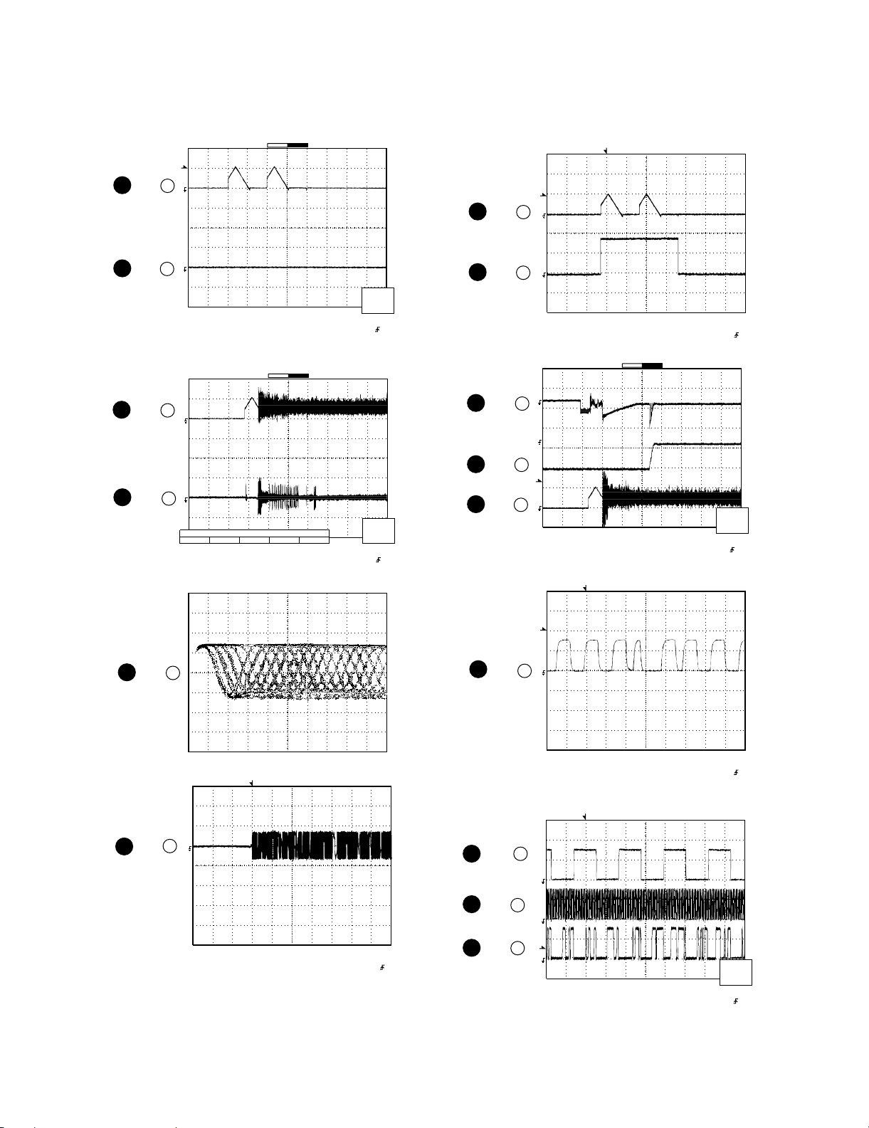
CHAPTER 5. CIRCUIT DESCRIPTION
[1] WAVEFORMS OF CD CIRCUIT
XL-MP40H
1
2
1
3
IC801 22
IC801 23
IC801 22
IC801 16
Stopped
CH1=500 mV
DC 10:1
T
FDO
1
TDO
3
Smoothing : ON CH1 : 0.000 V
BW : FULL
1
3
Smoothing : ON CH1 : 0.000 V
BW : FULL
CH2 : 0.0 V
CH3 : 0.000 V
CH4 : 0.00 V
Stopped
CH1=500 mV
DC 10:1
FDO
TE
-3 div -1 div 0 div +1 div +3div
CH2 : 0.0 V
CH3 : 0.00 V
CH4 : 0.00 V
CH2=10 V
DC 10:1
CH Position To
CH3=500 mV
DC 10:1
=Record Length=
Main : 100 K
Zoom : 2 K
CH3=1 V
DC 10:1
=Record Length=
Main : 100 K
Zoom : 2 K
500 ms/div
(500 ms/div)
NORM:20 kS/s
CH1
v/DIV
500 mV
=Trigger==Filter= =Offset=
Mode : AUTO
Type : EDGE CH1
Delay : 0.0ns
Hold off : 0.2 µs
500 ms/div
(500 ms/div)
NORM:20 kS/s
CH2
Position
0.20 div
=Trigger==Filter= =Offset=
Mode : AUTO
Type : EDGE CH1
Delay : 0.0ns
Hold off : 0.2 µs
1
5
6
7
1
IC801 22
IC801 25
IC801 28
IC801 27
IC801 22
Stopped
CH1=200 mV
DC 10:1
T
FDO
2
SPDO
1
Smoothing : ON CH1 : 0.000 V
BW : FULL
Stopped
CH1=500 mV
DC 10:1
PDOUT0
3
4
PDOUT1
T
FDO
1
Smoothing : ON CH1 : 0.000 V
BW : FULL
Stopped
CH1=2 V
DC 10:1
T
T
CH2=500 mV
DC 10:1
CH2 : 0.000 V
CH3 : 0.00 V
CH4 : 0.00 V
CH2 : 0.0 V
CH3 : 0.00 V
CH4 : 0.00 V
T
=Record Length=
Main : 100 K
Zoom : 2 K
CH3=1 V
DC 10:1
=Record Length=
Main : 100 K
Zoom : 2 K
1999/04/07 09:51:15
NORM:20 kS/s
=Trigger==Filter= =Offset=
Mode : NORMAL
Type : EDGE CH2
Delay : 2.924 ms
Hold off : 0.2 µs
1999/04/05 17:33:17
CH4=1 V
500 ms/div
(500 ms/div)
DC 10:1
NORM:20 kS/s
=Trigger==Filter= =Offset=
Mode : AUTO
Type : EDGE CH2
Delay : 0.0 ns
Hold off : 0.2 µs
1999/04/07 09:25:28
NORM:200 MS/s
500 ms/div
(500 ms/div)
CH1
v/DIV
500 mV
500 ns/div
(500 ns/div)
4
IC801 16
3
IC801 2
Stopped
CH1=10 V
DC 10:1
TE
2
=Filter= =Offset=
Smoothing : ON CH1 : 0.0V
BW : FULL
T
CH2=1 V
DC 10:1
CH2 : 0.00 V
CH3 : 0.00 V
CH4 : 0.00 V
=Record Length=
Main : 100 K
Zoom : 2 K
Vp-p=1.0 V~1.3 V
0.5 mV/div,0.5 µsec/div
100 ms/div
(100 ms/div)
NORM:100 kS/s
=Trigger=
Mode : NORMAL
Type : EDGE CH1
Delay : 2.924 ms
Hold off : 0.2 µs
8
9
10
11
IC801 69
IC801 60
IC801 59
IC801 58
1
DOUT
=Filter= =Offset=
Smoothing : ON CH1 : 0.00 V
BW : FULL
1
2
T
3
Smoothing : ON CH1 : 0.00 V
BW : FULL
Stopped
LRSY
DATACK
DATA
CH1=2 V
DC 10:1
CH2 : 0.00 V
CH3 : 0.00 V
CH4 : 0.00 V
T
CH2=2 V
DC 10:1
CH2 : 0.00 V
CH3 : 0.00 V
CH4 : 0.00 V
=Record Length=
Main : 1 K
Zoom : 100
CH3=2 V
DC 10:1
=Record Length=
Main : 5 K
Zoom : 100
=Trigger=
Mode : NORMAL
Type : EDGE CH1
Delay : 2.887 ms
Hold off : 0.2 µs
1999/04/05 20:50:17
5 µs/div
(5 µs/div)
NORM:100 kS/s
CH3
v/DIV
=Trigger==Filter= =Offset=
Mode : AUTO
Type : EDGE CH3
Delay : 0.0 ns
Hold off : 0.2 µs
2V
5 – 1
XL-MP40H
[2] VOLTAGE
PIN
NO.
10
11
12
13
PIN
NO.
PIN
NO.
PIN
NO.
PIN
NO.
1
2
3
4
5
6
7
8
9
1
2
3
4
5
6
7
8
9
10
11
12
13
14
15
16
17
18
19
20
21
22
23
24
25
26
27
28
29
30
31
32
33
34
35
36
1
2
3
1
2
3
1
2
3
IC101
VOLTAGE
4.13V
1.63V
0V
1.63V
1.55V
12V
18.2V
9.2V
0V
0V
0V
9.3V
0V
IC301
VOLTAGE
2.2V
2.2V
2.45V
0V
5V
5V
2.2V
2.2V
4V
3.86V
2.85V
2.28V
2.28V
0V
0V
0V
0V
3.4V
1.26V
1.7V
3.43V
2.2V
2.3V
0V
2.6V
2.14V
2.14V
1.3V
2.7V
1V
4.9V
4.9V
4.9V
4.9V
0V
1V
IC680
VOLTAGE
5.1V
0V
10.6VV
IC681
VOLTAGE
5.1V
0V
20V
IC705
VOLTAGE
5.7V
0.6V
10V
PIN
NO.
10
11
12
13
14
15
16
17
18
19
20
21
22
23
24
25
26
27
28
PIN
NO.
1
2
3
4
5
6
7
8
9
1
2
3
4
5
6
7
8
9
10
11
12
13
14
15
16
17
18
19
20
21
22
23
24
25
26
27
28
29
30
IC401
VOLTAGE
0V
0V
0V
0V
0V
0V
0V
0V
0V
0V
0V
4.5V
0.7V
-4.5V
0V
0V
0V
0V
0V
0V
0V
0V
0V
0V
0V
0V
0V
0V
IC802
VOLTAGE
7.75V
2.77V
1.45V
1.47V
3.9V
3.3V
0V
0V
0V
3.5V
3.7V
1.46V
1.45V
2.9V
1V
2.9V
3.4V
1.45V
1.45V
3.7V
3.6V
0V
0V
0V
3.6V
3.6V
1.46V
1.46V
1.46V
7.8V
PIN
NO.
10
11
12
13
14
15
16
17
18
19
20
21
22
23
24
25
26
27
28
29
30
31
32
33
34
35
36
37
38
39
40
41
42
43
44
45
46
47
48
49
50
51
52
53
54
55
56
57
58
59
60
61
62
63
64
65
66
67
68
69
70
71
72
73
74
75
76
77
78
79
80
1
2
3
4
5
6
7
8
9
IC801
VOLTAGE
1.38V
1.47V
1.45V
1.2V
1.6V
1.7V
1.67V
1.63V
1.42V
1.4V
1.46V
1.74V
1.75V
1.74V
1.43V
1.43V
1.43V
2V
0.18V
0V
2.9V
1.47V
1.5V
1.5V
1.6V
0V
0V
1V
0.93V
2.74V
0V
2.8V
0V
2.8V
0V
2.8V
0V
1.8V
2.8V
0V
2.8V
0V
0.45V
3V
3V
0V
3.23V
2.8V
2.8V
2.8V
0V
0V
0V
0V
0V
0V
0V
0V
0V
0V
2.57V
1.44V
2.1V
2.1V
0V
1.8V
0V
2.8V
0V
0V
0V
1V
1.14V
2.7V
1.64V
3.3V
0V
1.64V
2.9V
1.4V
PIN
NO.
PIN
NO.
PIN
NO.
PIN
NO.
PIN
NO.
PIN
NO.
E
C
B
E
C
B
E
C
B
E
C
B
E
C
B
VOLTAGE
1
2
3
4
5
6
7
8
9
10
11
12
13
14
15
16
17
18
19
20
21
22
23
24
25
26
27
28
29
30
31
32
33
34
35
36
37
38
39
40
41
42
43
44
45
46
47
48
49
50
Q104
VOLTAGE
0V
3.3V
0.54V
Q206
VOLTAGE
5V
-9V
5V
Q207
VOLTAGE
-3V
0V
-9V
Q208
VOLTAGE
-3V
0V
-9V
Q209
VOLTAGE
-3V
0V
9V
0V
0V
0V
0V
0V
0V
0V
0V
0V
0V
5V
1.7V
2.4V
0V
0V
0V
5V
0V
5V
0.5V
0V
0V
0V
5V
0V
5V
0V
5V
0V
0V
4.5V
0V
5V
0V
0V
5V
0V
0V
0V
0V
0V
0V
0V
0V
0V
2.4V
2.4V
0V
2.4V
2.4V
IC701
PIN
NO.
51
52
53
54
55
56
57
58
59
60
61
62
63
64
65
66
67
68
69
70
71
72
73
74
75
76
77
78
79
80
81
82
83
84
85
86
87
88
89
90
91
92
93
94
95
96
97
98
99
100
PIN
NO.
PIN
NO.
PIN
NO.
PIN
NO.
PIN
NO.
E
C
B
E
C
B
E
C
B
E
C
B
E
C
B
VOLTAGE
2.4V
2.4V
2.4V
4.8V
0V
2.4V
2.4V
2.4V
2.4V
2.4V
2.4V
2.4V
2.4V
2.4V
2.4V
2.4V
2.4V
2.4V
2.4V
2.4V
2.4V
2.4V
2.4V
2.4V
2.4V
2.4V
2.4V
2.4V
2.4V
0V
1.7V
3.3V
2.4V
2.4V
2.4V
2.4V
0V
0V
0V
5V
0V
0V
0V
0V
0V
5V
0V
0V
0V
0V
Q214
VOLTAGE
0V
5V
0V
Q215
VOLTAGE
9.3V
9.2V
8.5V
Q216
VOLTAGE
0V
0V
4V
Q217
VOLTAGE
9.3V
0V
9.3V
Q218
VOLTAGE
0V
9.3V
0V
PIN
NO.
C
PIN
NO.
PIN
NO.
PIN
NO.
PIN
NO.
PIN
NO.
C
PIN
NO.
C
PIN
NO.
C
PIN
NO.
PIN
NO.
PIN
NO.
PIN
NO.
E
B
E
C
B
E
C
B
E
C
B
E
C
B
E
B
E
B
E
B
E
C
B
E
C
B
E
C
B
E
C
B
Q237
VOLTAGE
0V
4.8V
0V
Q238
VOLTAGE
4.9V
4.9V
1.2V
Q303
VOLTAGE
0V
3.6V
0.8V
Q410
VOLTAGE
0V
0V
0V
Q411
VOLTAGE
0V
0V
0V
Q611
VOLTAGE
-5V
-12.7V
-5.6V
Q612
VOLTAGE
20V
20V
0.7V
Q613
VOLTAGE
20V
20V
5.1V
Q655
VOLTAGE
3.5V
18V
9.1V
Q657
VOLTAGE
0V
0V
0.7V
Q658
VOLTAGE
9.3V
17.2V
9.9V
Q659
VOLTAGE
18V
18V
0.6V
PIN
NO.
C
PIN
NO.
C
PIN
NO.
C
PIN
NO.
C
PIN
NO.
C
PIN
NO.
C
PIN
NO.
C
PIN
NO.
C
PIN
NO.
C
PIN
NO.
C
PIN
NO.
C
PIN
NO.
C
E
B
E
B
E
B
E
B
E
B
E
B
E
B
E
B
E
B
E
B
E
B
E
B
Q660
VOLTAGE
11V
11V
0.7V
Q661
VOLTAGE
18V
18V
0.7V
Q662
VOLTAGE
0V
0V
4V
Q663
VOLTAGE
5V
5V
0.6V
Q664
VOLTAGE
1.3V
1.3V
0.7V
Q665
VOLTAGE
-12V
-12V
-8V
Q701
VOLTAGE
0V
4.8V
0V
Q703
VOLTAGE
0V
0V
0.7V
Q704
VOLTAGE
0V
5V
0V
Q705
VOLTAGE
0V
0V
0.8V
Q801
VOLTAGE
2.76V
1.8V
2V
Q802
VOLTAGE
2.9V
6.3V
3.6V
PIN
NO.
PIN
NO.
PIN
NO.
PIN
NO.
E
C
B
E
C
B
E
C
B
E
C
B
Q805
VOLTAGE
3.27V
5V
3.93V
Q806
VOLTAGE
7.9V
18.1V
8.55V
Q301
VOLTAGE
10.5V
18V
11V
Q302
VOLTAGE
1V
2.7V
1.7V
5 – 2
AudioXL-MP40HService ManualXLMP40HMarketE
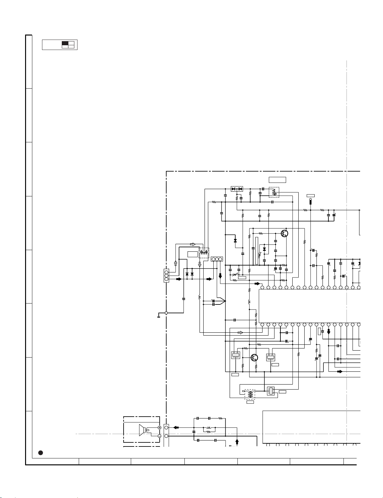
CHAPTER 6. CIRCUIT SCHEMATICS AND PARTS LAYOUT
[1] NOTES ON SCHEMATIC DIAGRAM
XL-MP40H
•Resistor:
To differentiate the units of resistors, such symbol as K and M are
used: the symbol K means 1000 ohm and the symbol M means
1000 kohm and the resistor without any symbol is ohm-type resistor. Besides, the one with “Fusible” is a fuse type.
• Capacitor:
To indicate the unit of capacitor, a symbol P is used: this symbol P
means micro-micro-farad and the unit of the capacitor without such
a symbol is microfarad. As to electrolytic capacitor, the expression
“capacitance/withstand voltage” is used.
(CH), (TH), (RH), (UJ): Temperature compensation
(ML): Mylar type
(P.P.): Polypropylene type
• Schematic diagram and Wiring Side of P.W.Board for this model
are subject to change for improvement without prior notice.
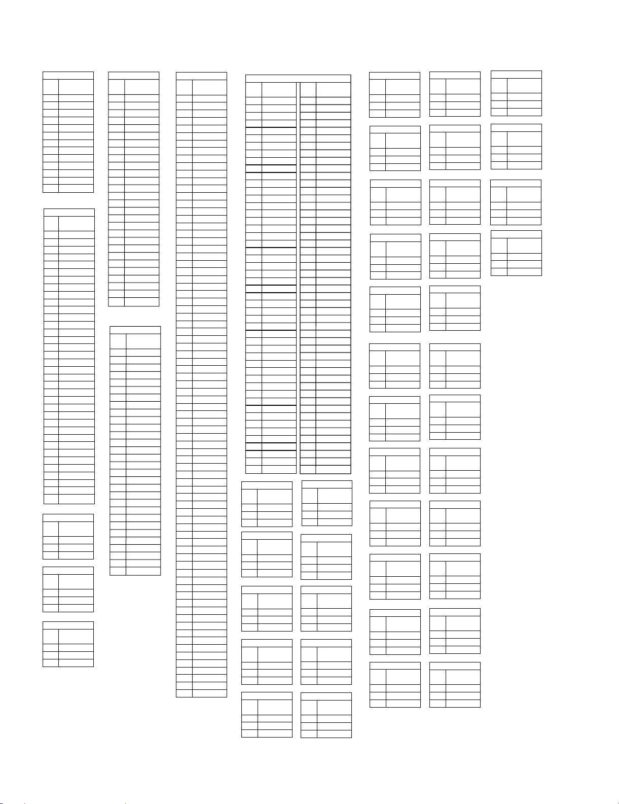
REF. NO DESCRIPTION POSITION
SW700 VOLUME ON—OFF
SW701 ON/STAND-BY ON—OFF
SW702 STOP/TUNING DOWN ON—OFF
SW703 REW/PRESET DOWN ON—OFF
SW704 PLAY/CD PAUSE/TUNING UP ON—OFF
SW705 MEMORY/SET ON—OFF
• The indicated voltage in each section is th e one measured by Digital Multimeter between such a section and the chassis with no signal given.
1. In the tuner section,
( ) indicates AM
< > indicates FM stereo
2. In the main section, a tape is being played back.
3. In the deck section, a tape is being played back.
( ) indicates the record state.
4. In the power section, a tape is being played back.
5. In the CD section, the CD is stopped.
• Parts marked with “ ” ( ) are important for
maintaining the safety of the set. Be sure to replace these parts
with specified ones for maintaining the safety and performance of
the set.
REF. NO DESCRIPTION POSITION
SW706 FUNCTION ON—OFF
SW707 REC/PAUSE ON—OFF
SW708 BASS/TREBLE ON—OFF
SW709 FF/PRESET UP ON—OFF
SW710 DISC EJECT ON—OFF
SW901 FOOL PROOF ON—OFF
SW902 PLAY ON—OFF
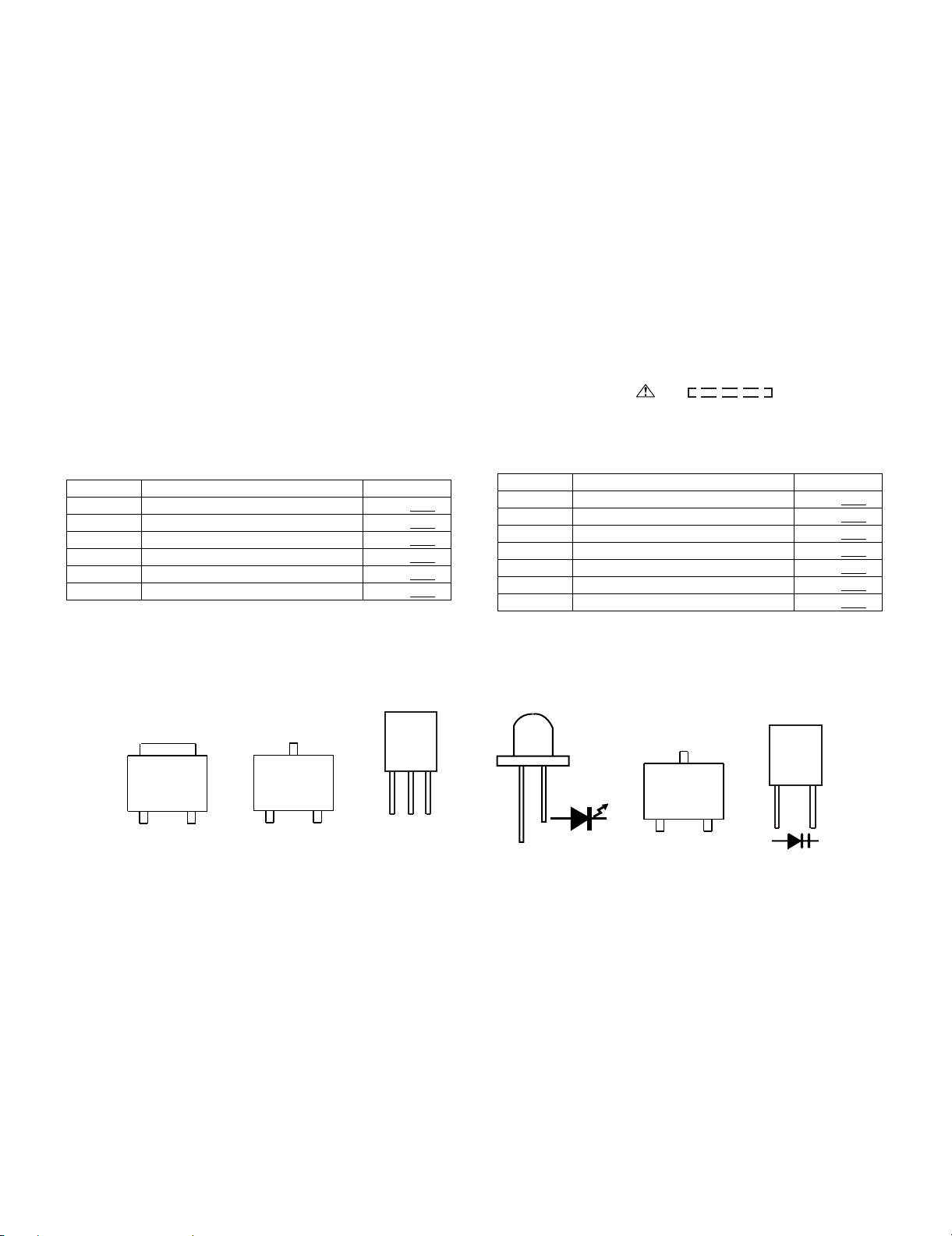
[2] TYPES OF TRANSISTOR AND LED
C
B
2SK2541
E
C
B
2SC3052 F+
2SC5477++
2SA1235 F+
E
FRONT
EC B
(S) (G) (D)
(1) (2) (3)
2HA1015 GR
2HC1815 GR
KTC3200 GR
2SB562 C
KRC101 M
2SB561 C
KRC106 M
KRC107 M
KRA107 M
KTC2026 Y
VIEW
FRONT
VIEW
FRONT
VIEW
SVC347SMPG3372X
SVC201
6 – 1
XL-MP40H
POWER AMP.
0
2
1/50
1/50
0.1
22/50
100K
12P
(CH)
0.018
1µH
1SS133
0
0.1
3.3K
4.7/50
0.001
22/50
0.033
10K
10K
33
2.2K
680
47µH
47/50
1SS133
1/50
0.01
0.01
0.1
22/50
100K
4.7K
0.01
1K
100K
27P
(UJ)
4.7K
0.33/50
100P
(CH)
5P
33P
(CH)
(UJ)
0.015
1K
33P
(CH)
330
5P
0.001
SVC201
2.2K
0.047
100
10µH
10
560P
0.0047
0.001
0.022
SVC201
100K
220
0.01
100K
0
0.001
0.01
10P
(UJ)
10
0
330
22/50
M
1/50
0.0047
10
0.1
10
0.1
0.0047
0.0047
LA4631++
2
1
3
2
1
4
5
6
7
8
9
10
11
1213
123
1362 3 4 5 6 7 8 9 10 11 12 13 14 15 16 17
20212223242526272829303132333435
SVC347S
NC
GND2
AMRF-IN
REG
FM-MIX
GND1
AM-MIX
VCC1
AMIFIN
FMIFIN
VSS
CE
P-DET
P-CCMP
FMDET
L-OUT
R-OUT
DI
CL
XOUT
VDD
MPX-IN
DET-OUT
AMLOWOUT
AGC
PD
LP-IN
LP-OUT
B01
B02
AM-OSC
FM-OSC
VCC2
FMRF-OUT
FMRF-IN
OUT1
P_GND
OUT2
VCC
P.P
STBY
IN2
6
5
4
3
1
2
6
4
3
2
1
L-CH
AM
GND
FM
FROM FM/AM ANTENNA
2SC5477++
SPEAKER BOX Ass'y
FM RF
FM BAND COVERAGE fL
AM
Tracking
BAND PASS
FILTER
AM IF
AM IF
FM IF
FM IF
TP-VT
AM BAND
COVERAGE fL
FM IF
CHASSIS
GND
2SC5477++
D305
R303
C305
C308
R310
R315
C318
R311
R304
C310
L306
C311
C348
JR304
C326
C330
C
C333
C332
C329
R316
C335
Z
C325
R313
R314
C321
C320
C346
C345
C344
C312
R308
C316
R329
C343
C317 L307
D307
R328
Q302
JP302
L304
R307
C314
R305
C309
C307
R306
L302
C349
C306
BF301
D306
L301
D303
D302
C301
C302
CNP301
C347
L303
R336
R334
R332
C319
C313
C315
CF302
C327
JR303
C323
R309
R312
CF303
R331
Q303
R333
CF301
C322
C331
L30
C32
C32
CF304
L305
IC101
R107
L103
R103
C105
C109
C103
C131
C130
C107
R327
R302
C303
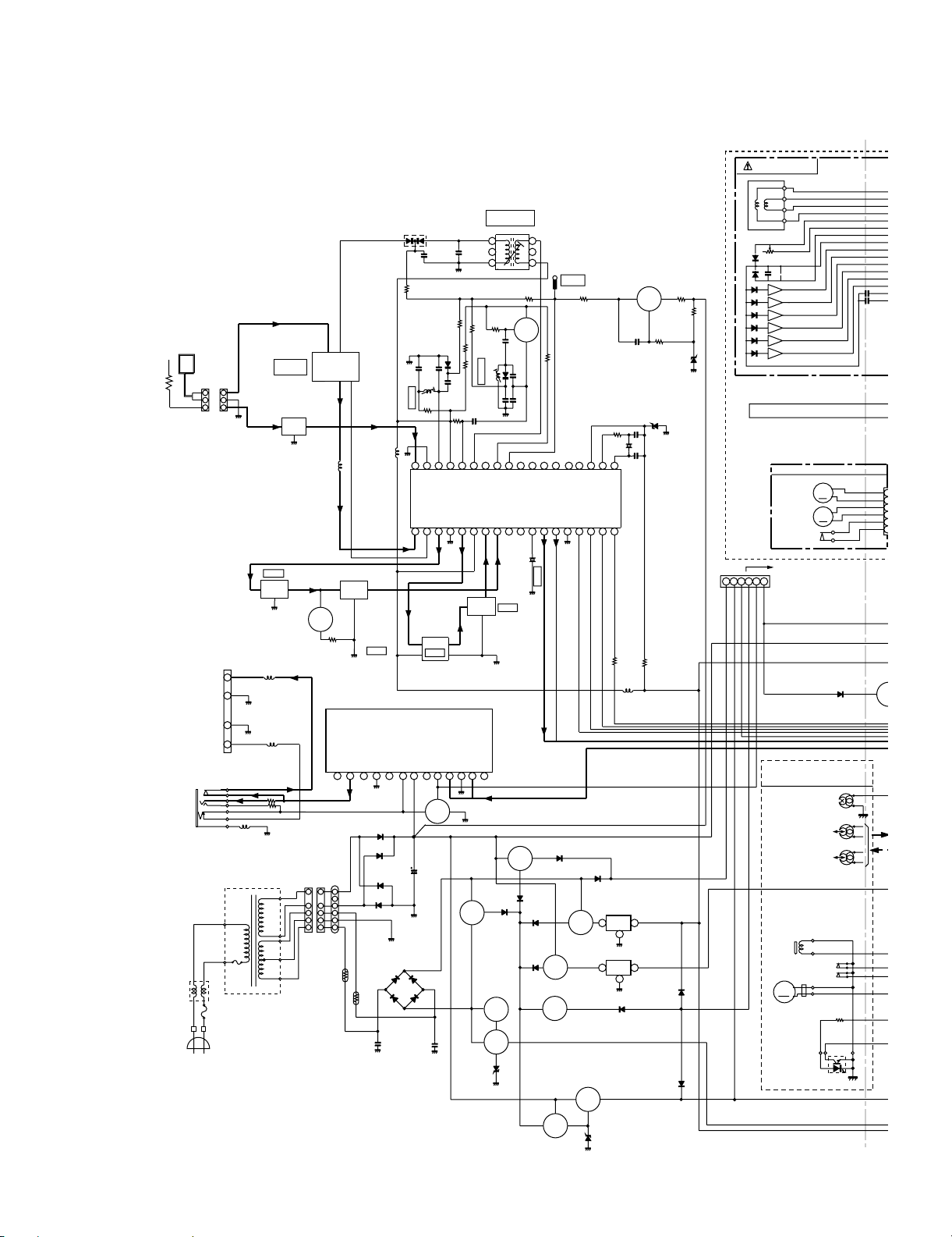
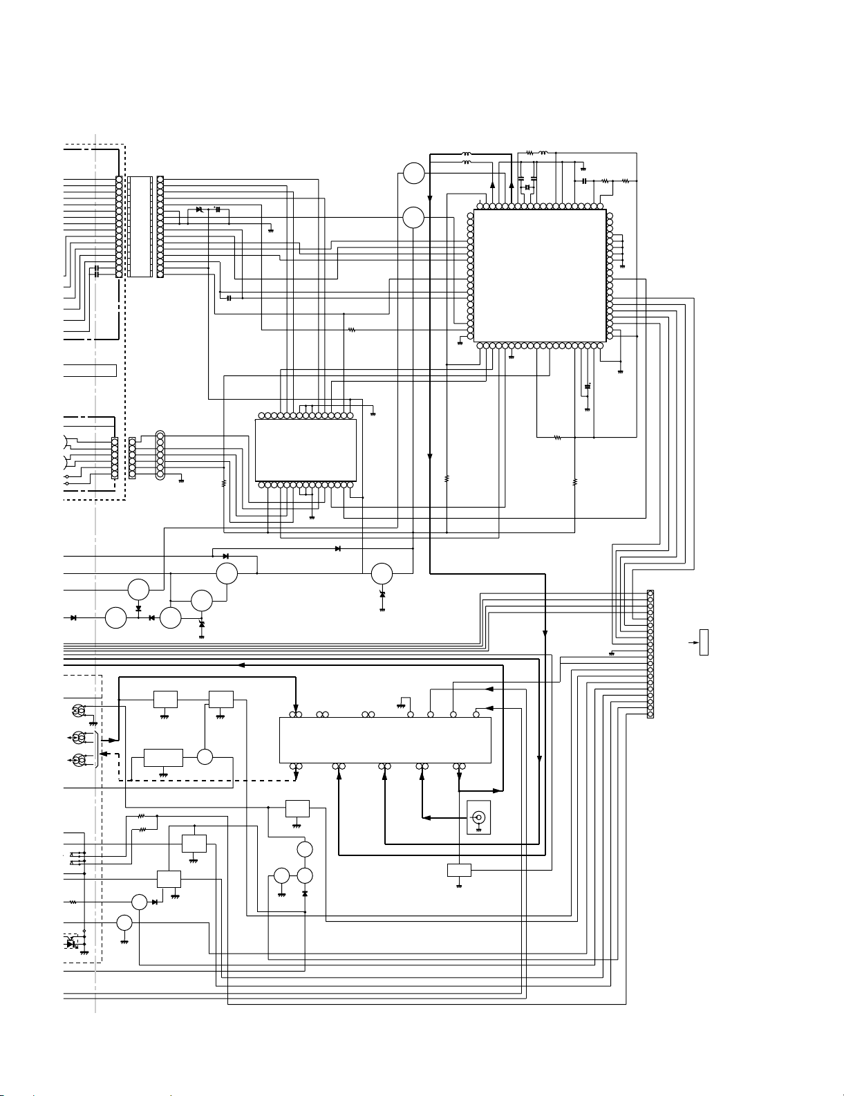
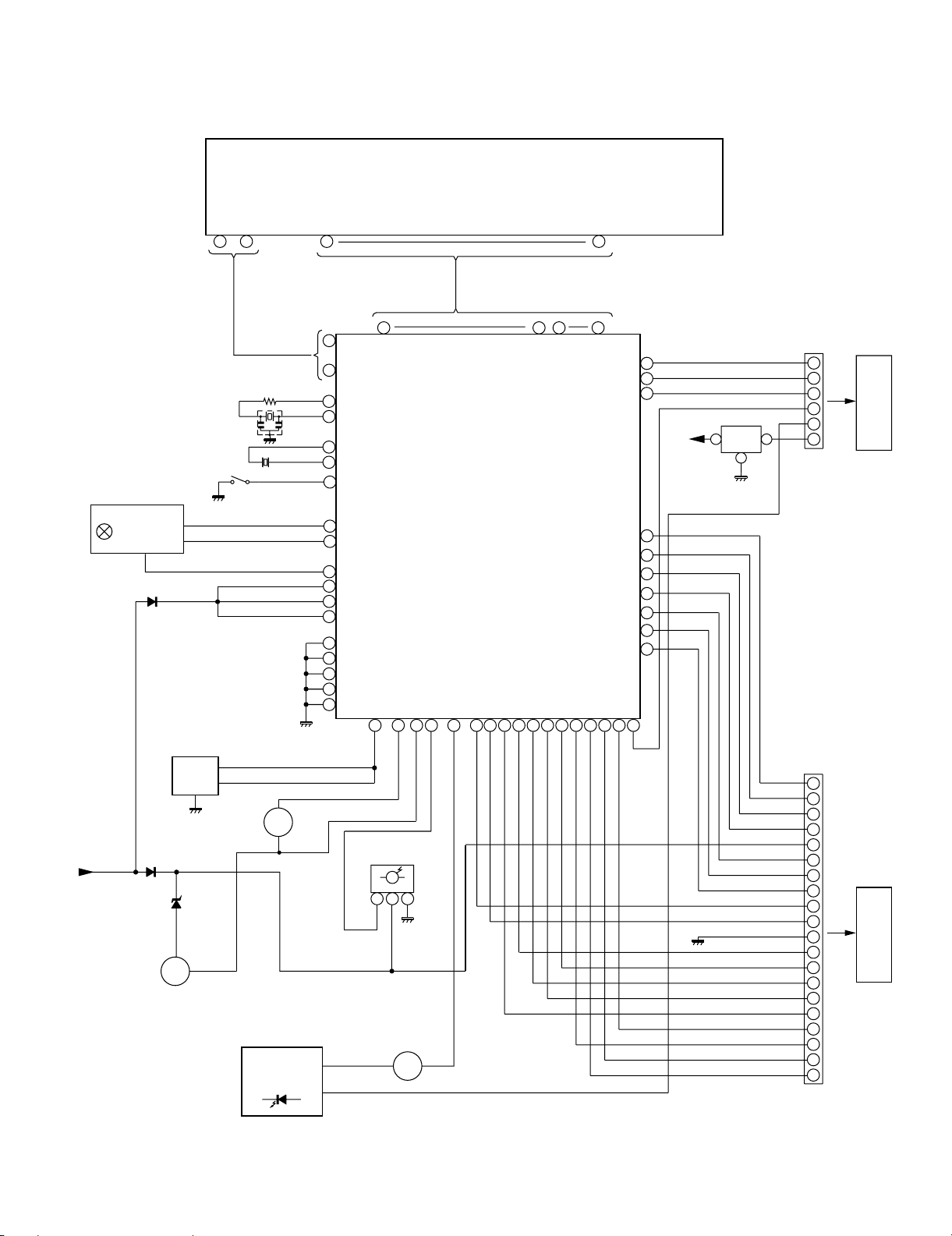
[3] WIRING SIDE OF PWB/SCHEMATIC DIAGRAM
MAIN
A
B
C
D
E
F
G
H
NOTES ON SCHEMATIC DIAGRAM can be found on page 6-1
1
23456
Figure 6-2 SCHEMATIC DIAGRAM (1/10)
6 – 2
 Loading...