Sony XDP-4000X Service Manual
XDP-4000X
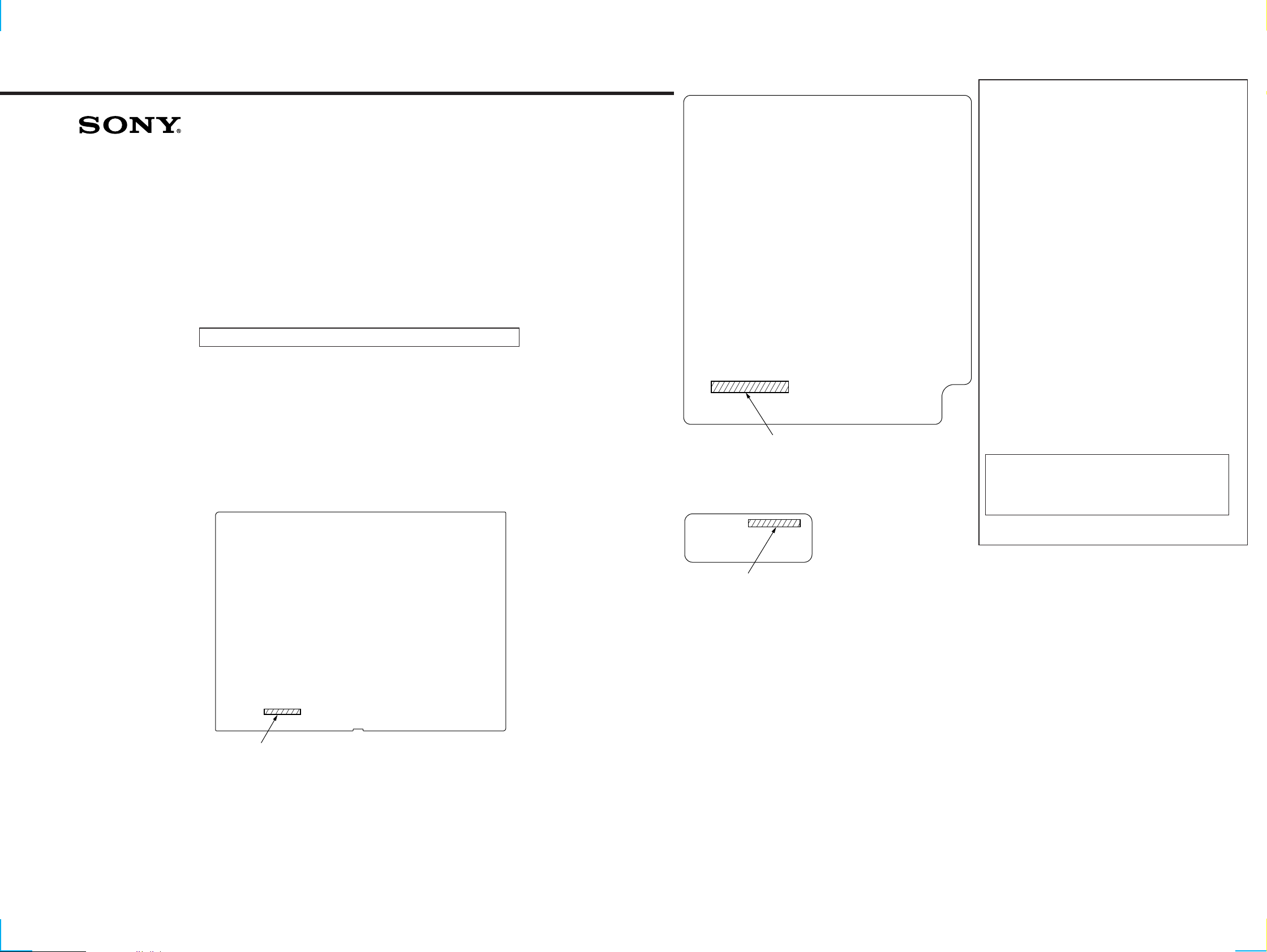
INDICATOR Board Part No.
Former type : 1-671-415-11
New type : 1-671-415-13
– INDICATOR BOARD (SIDE A) –
SERVICE MANUAL
SUPPLEMENT-1
File this supplement with the service manual.
Subject : Change of Main, DAC and Indicator Boards
Printed wiring boards and schematic diagram of new type, and changed parts
list are described in this supplement-1.
Refer to original service manual (9-926-036-S) previously issued for the other
information.
When performing service and inspection, check the suffix of the part number of
the main, DAC and indicator boards.
1. DISCRIMINATION
– MAIN BOARD (SIDE A) –
Canadian Model
(ECN-A00603)
US Model
AEP Model
UK Model
E Model
– DAC BOARD (SIDE A) –
DAC Board Part No.
Former type : 1-671-417-11
New type : 1-671-417-13
THIS NOTE IS COMMON FOR PRINTED WIRING BOARDS
AND SCHEMATIC DIAGRAMS.
(In addition to this, the necessary note is
printed in each block.)
For schematic diagrams
• All capacitors are in µF unless otherwise noted. pF: µµF
50 WV or less are not indicated except for electrolytics
and tantalums.
• All resistors are in Ω and 1/
specified.
• % : indicates tolerance.
f
•
• C : panel designation.
• U : B+ Line.
• Power voltage is dc 14.4V and fed with regulated dc power
• Voltage is dc with respect to ground under no-signal
• Voltages are tak en with a V OM (Input impedance 10 MΩ).
• Signal path.
• (( )) : Page of service manual.
For printed wiring boards
• X : parts extracted from the component side.
•
• b : Pattern from the side which enables seeing.
Caution:
Pattern face side: Parts on the pattern face side seen from the
(Side B) pattern face are indicated.
Parts face side: Parts on the parts face side seen from the
(Side A) parts face are indicated.
• (( )) : Page of service manual.
: internal component.
supply from B+ cord and Master unit.
condition.
Voltage variations may be noted due to normal produc-
tion tolerances.
F : ANALOG
J : DIGITAL
<< >> : Page of supplement-1.
a
: Through hole.
(The other layer’s patterns are not indicated.)
<< >> : Page of supplement-1.
4
W or less unless otherwise
MAIN Board Part No.
Former type : 1-671-416-11
New type : 1-671-416-13
11
XDP-4000X
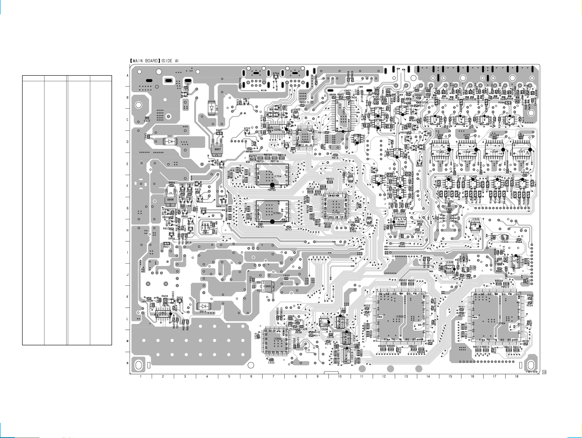
• Semiconductor Location (Side A)
Ref. No. Location Ref. No. Location
D100 B-12
D101 B-11
D102 B-13
D104 B-12
D105 B-11
D106 B-13
D200 B-12
D201 B-13
D202 B-14
D204 B-12
D205 B-12
D206 B-14
D701 C-7
D702 C-7
D703 B-7
D704 A-7
D707 D-8
D901 D-2
D902 F-3
D903 F-3
D906 F-4
D907 G-5
D908 G-4
D910 H-3
D911 E-5
D914 K-4
D916 B-3
D917 B-4
D919 H-2
D922 K-3
D923 K-2
D950 E-13
IC101 C-13
IC102 C-12
IC103 F-13
IC110 E-12
IC111 F-12
IC202 C-12
IC203 F-13
IC303 D-14
IC304 C-14
IC306 D-16
IC307 C-15
IC309 D-17
IC310 C-17
IC312 D-18
IC313 C-18
IC401 F-15
IC405 F-16
IC408 F-17
IC411 F-18
IC501 H-13
IC502 M-7
IC503 L-13
IC504 L-17
2. PRINTED WIRING BOARD — MAIN SECTION —
IC506 L-9
IC507 M-10
IC508 J-15
IC509 J-16
IC510 L-10
IC511 I-17
IC513 N-10
IC514 I-18
IC520 H-16
IC521 F-10
IC522 H-17
IC603 C-10
IC604 D-8
IC605 C-8
IC701 C-7
IC702 G-10
IC703 G-7
IC704 F-7
IC705 D-11
IC706 H-11
IC901 H-4
IC902 L-2
IC905 K-7
IC950 H-15
IC951 H-14
Q301 B-15
Q302 B-15
Q303 B-16
Q304 B-17
Q305 B-17
Q306 B-18
Q307 B-18
Q308 B-18
Q601 C-8
Q701 C-7
Q702 D-6
Q901 G-3
Q902 G-3
Q903 G-3
Q906 G-2
Q907 D-4
Q908 E-4
Q910 H-2
Q911 G-2
Q912 H-3
Q916 E-12
Q917 B-6
Q918 G-4
Q950 E-14
Q951 D-14
Q952 D-13
Q953 C-14
Q954 D-13
Q955 C-14
04
22
<<Page 9>> ((Page 37))
XDP-4000X
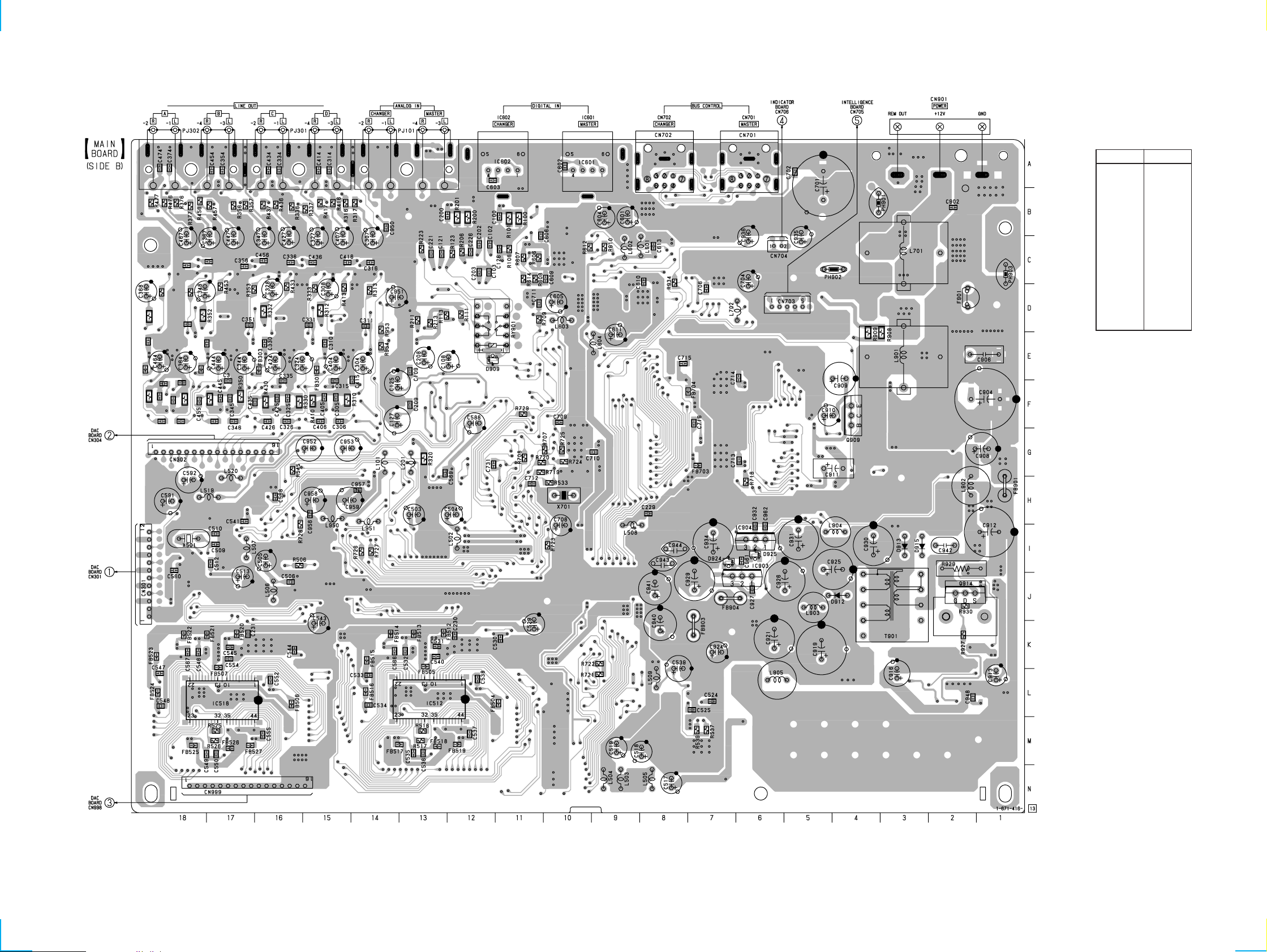
• Semiconductor
Location (Side B)
Ref. No. Location
D909 E-12
D912 J-4
D913 I-3
D915 I-3
D924 I-7
D925 I-6
IC512 L-13
IC518 L-17
IC601 A-10
IC602 A-11
IC903 J-6
IC904 I-6
Q909 F-4
Q914 J-2
<<Page 9>>
<<Page 9>>
<<Page 9>>
04
33
XDP-4000X
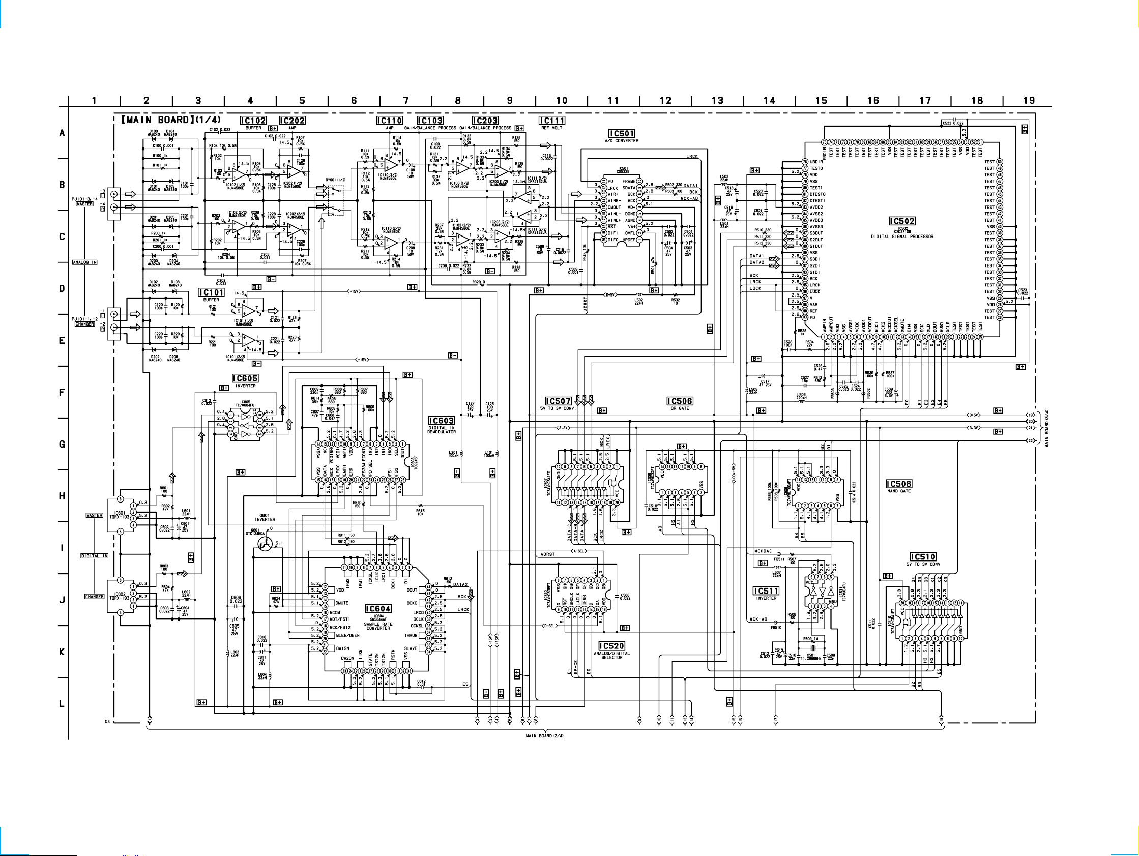
3. SCHEMATIC DIAGRAM — MAIN SECTION (1/4) —
<<Page 6>>
<<Page 5>>
44
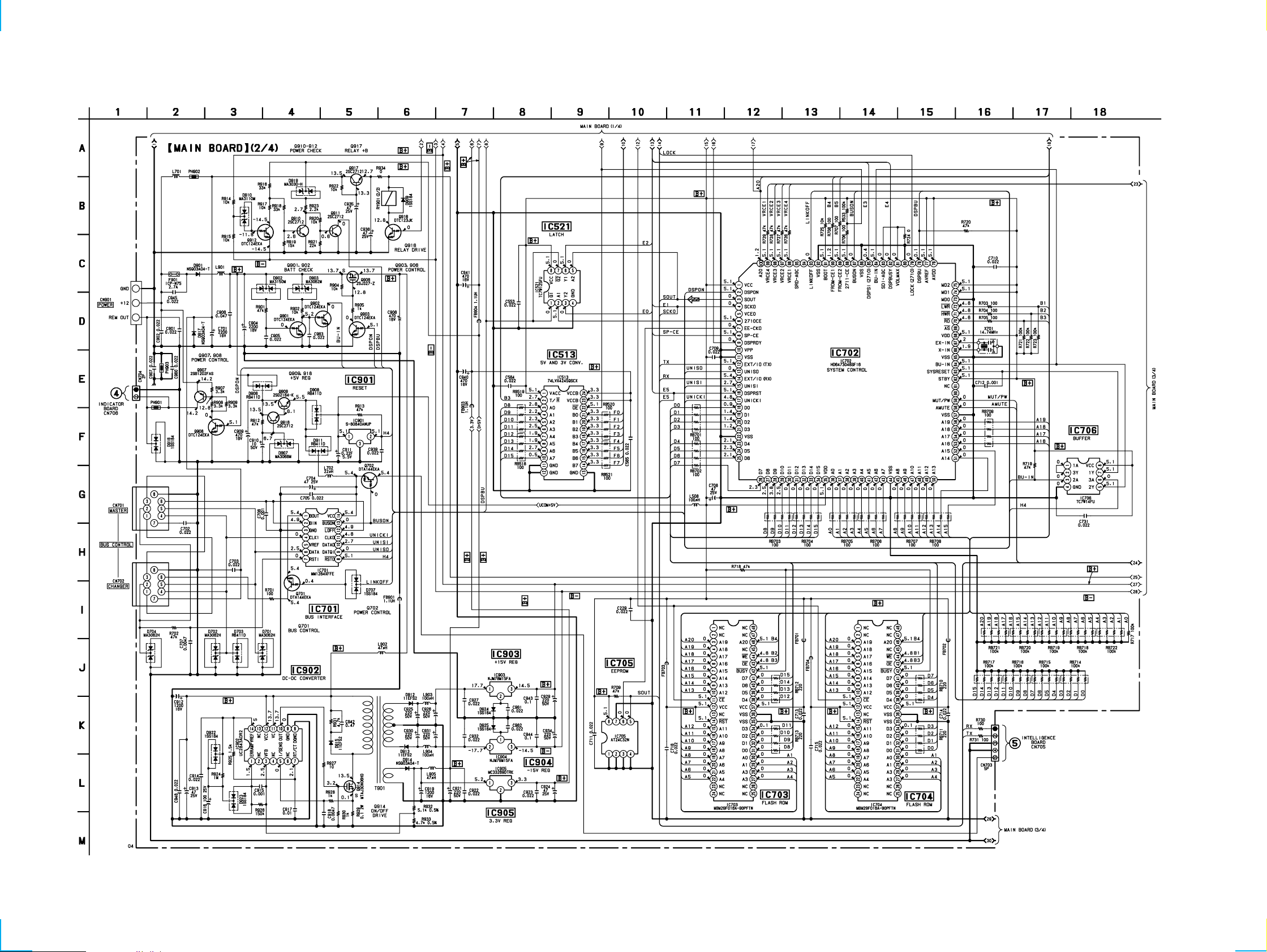
4. SCHEMATIC DIAGRAM — MAIN SECTION (2/4) —
XDP-4000X
<<Page 4>>
<<Page
8>>
<<Page 6>>
55
((Page 34))
<<Page 6>>
XDP-4000X
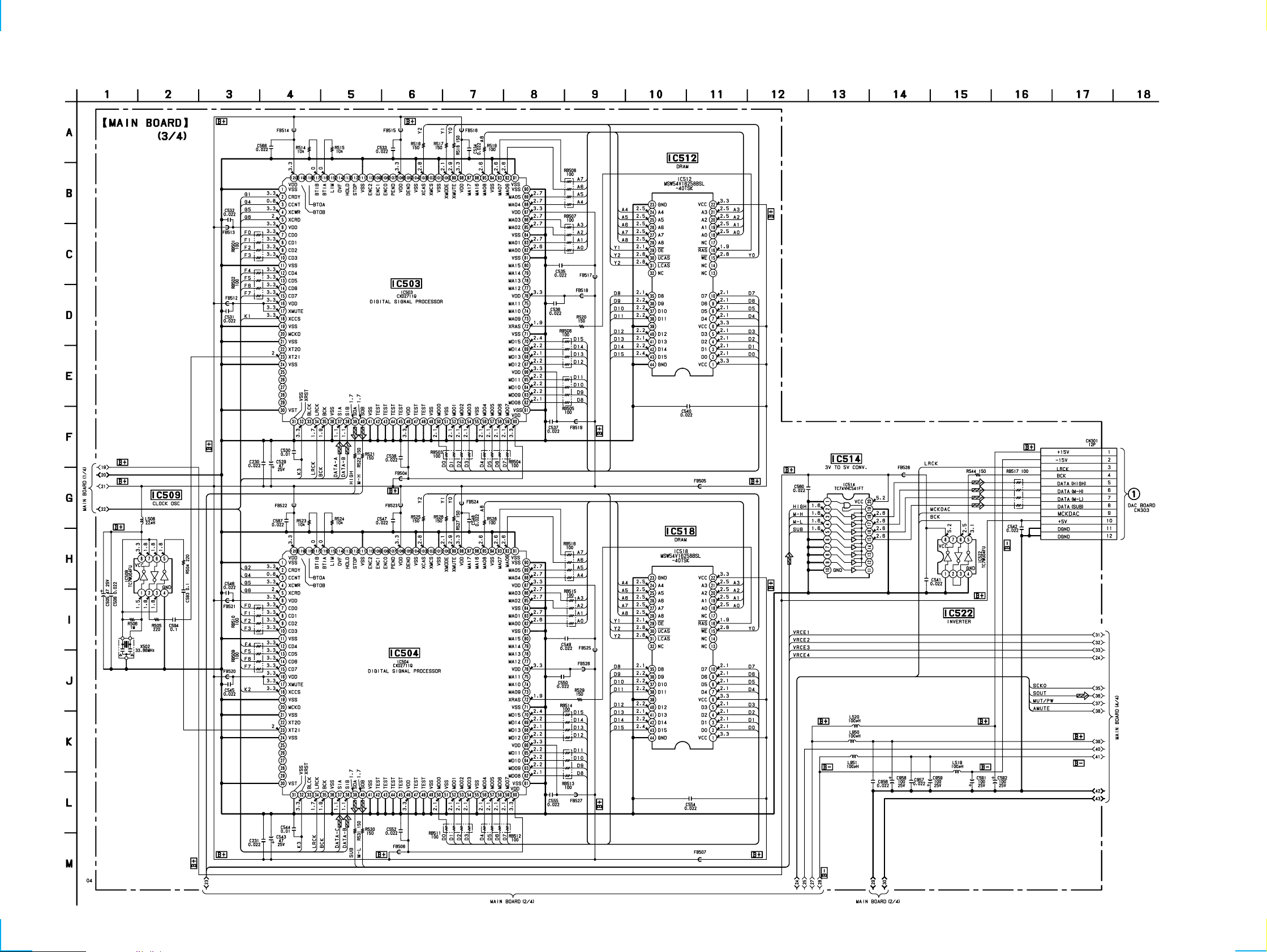
5. SCHEMATIC DIAGRAM — MAIN SECTION (3/4) —
<<Page 4>>
<<Page 8>>
<<Page 7>>
<<Page 5>>
66
<<Page 5>>
 Loading...