Sony XDP-4000-X Service manual
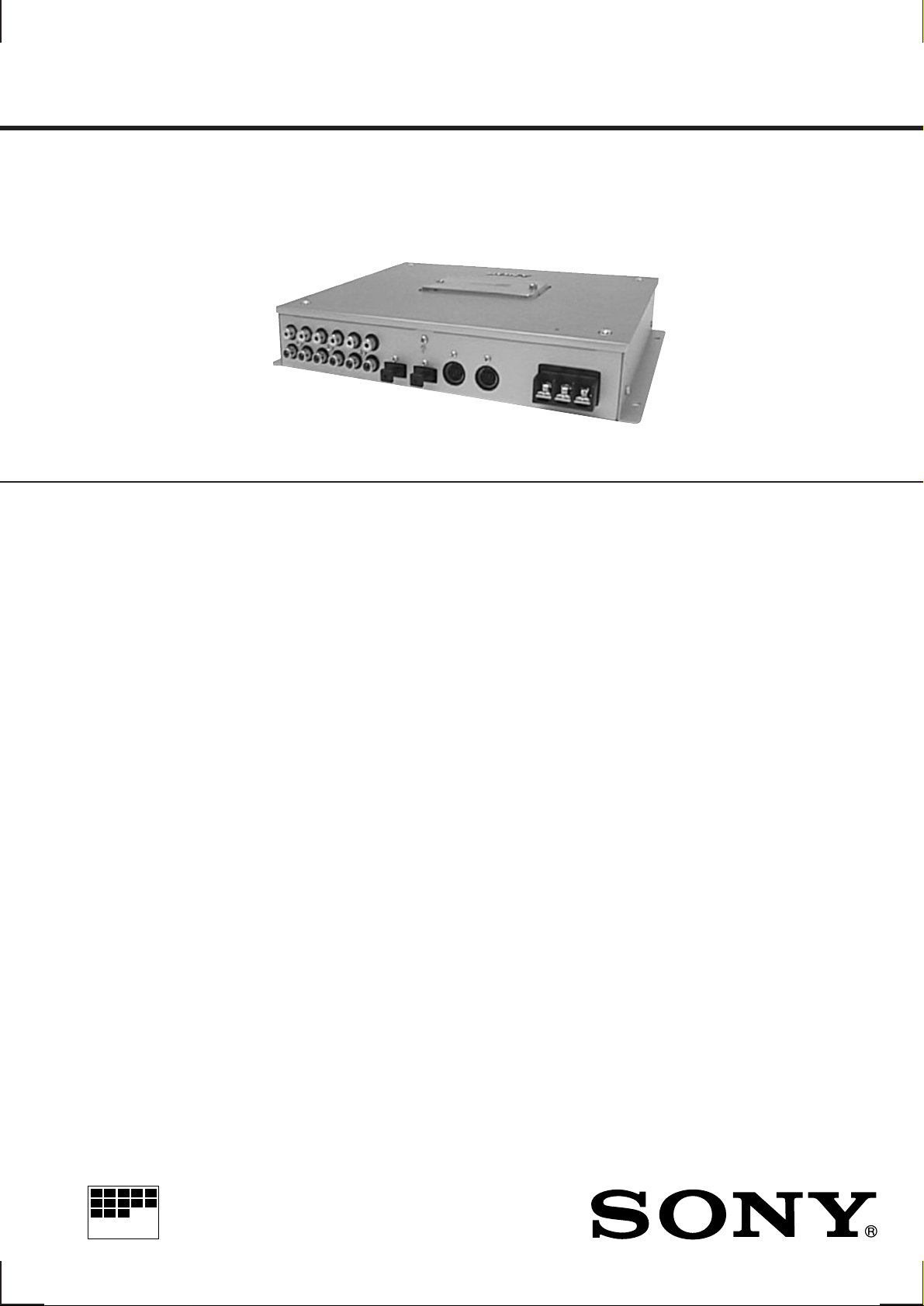
XDP-4000X
SERVICE MANUAL
SPECIFICATIONS
Power requirements 12 V DC car battery (negative
ground, 10.5 V – 16 V)
Current drain 1 A
Frequency response 5 Hz – 20 kHz
Signal-to-noise ratio 105 dB (Optical input)
Harmonic distortion 0.003 % (Optical input)
Separation 95 dB at 1 kHz
Input/output terminals BUS input (1)
BUS output (1)
Line input (RCA jack) (2)
Line output (RCA jack) (4)
Optical digital input (2)
Dimensions Approx. 249 × 45 × 183 mm
(9 7/8 × 1 13/16 × 7 1/4 in.) (w/h/d)
Mass Approx. 2 kg (4 lb. 7 oz.)
Design and specifications are subject to change without
notice.
US Model
Canadian Model
AEP Model
UK Model
E Model
MICROFILM
Notes on Chip Component Replacement
• Never reuse a disconnected chip component.
• Notice that the minus side of a tantalum capacitor may be dam-
aged by heat.
DIGITAL EQUALIZER PREAMPLIFIER
– 1 –
SECTION 1
SER VICE NOTE
TABLE OF CONTENTS
1. SERVICE NOTE................................................................. 2
2. GENERAL
Operation ................................................................................. 4
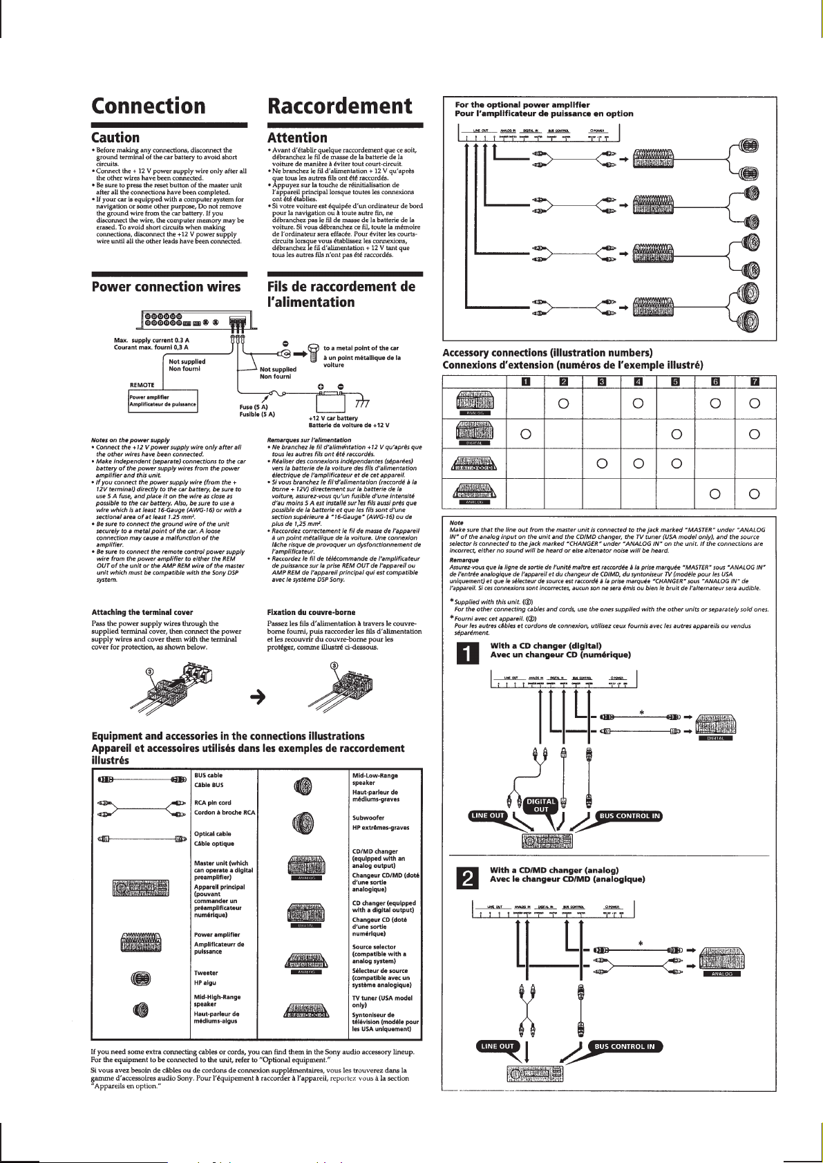
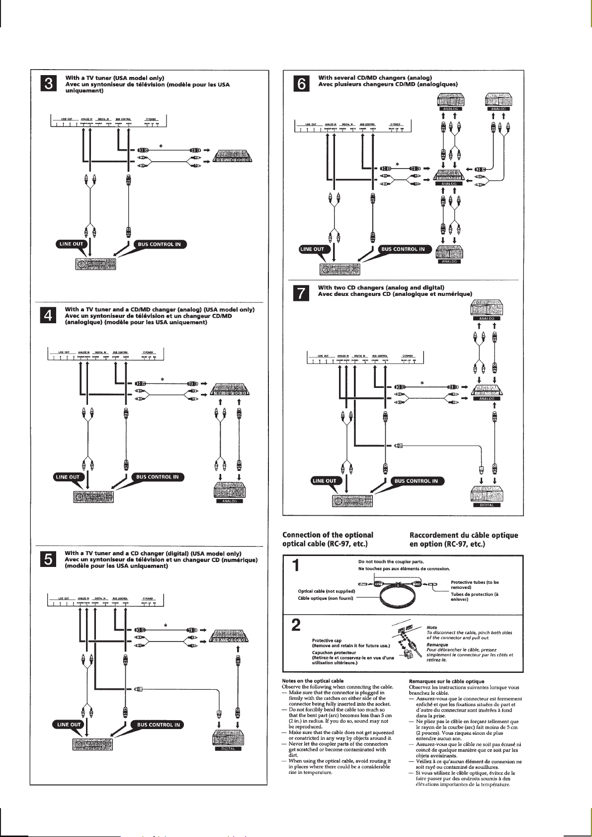
Connection............................................................................... 5
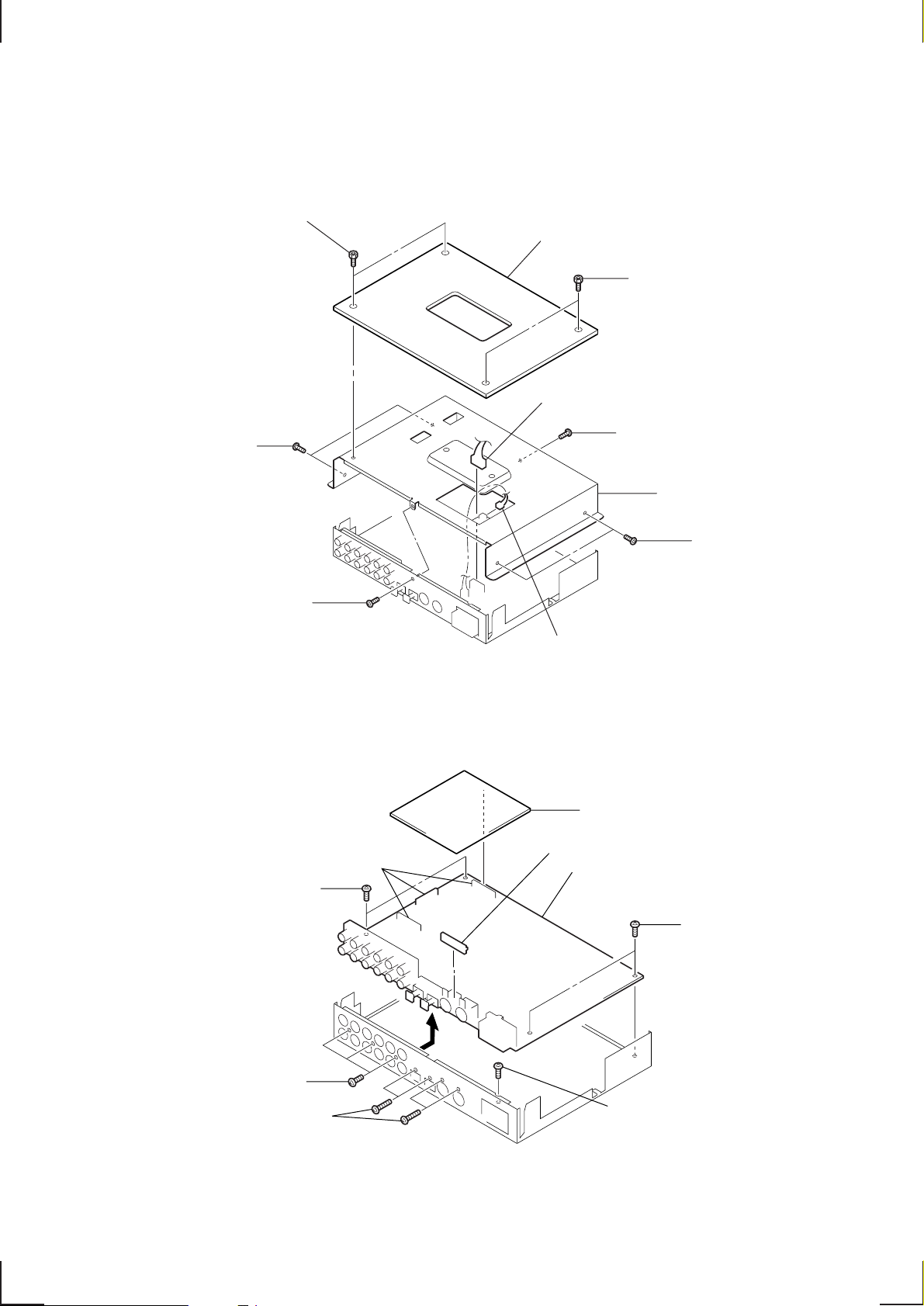
3. DISASSEMBLY
3-1. Case (Upper)....................................................................... 7
3-2. Main Board.........................................................................7
4. DIAGRAMS
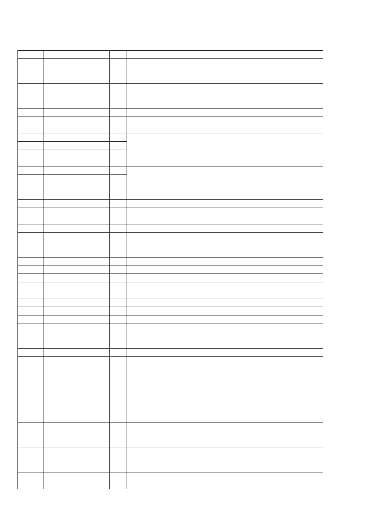
4-1. IC Pin Descriptions ............................................................ 8
4-2. Block Diagram – Input section –...................................... 15
4-3. Block Diagram – DSP section –.......................................17
4-4. Block Diagram – Output section – ................................... 19
4-5. Printed Wiring Board – Main Section – ........................... 21
4-6. Schematic Diagram – Main Section (1/4) – ..................... 25
4-7. Schematic Diagram – Main Section (2/4) – ..................... 27
4-8. Schematic Diagram – Main Section (3/4) – ..................... 29
4-9. Schematic Diagram – Main Section (4/4) – ..................... 31
4-10. Schematic Diagram – DAC, Intelligence,
Indicator Section –............................................................ 33
4-11. Printed Wiring Board – DAC Section – ........................... 35
4-12. Printed Wiring Boards – Intelligence,
Indicator Section –............................................................ 37
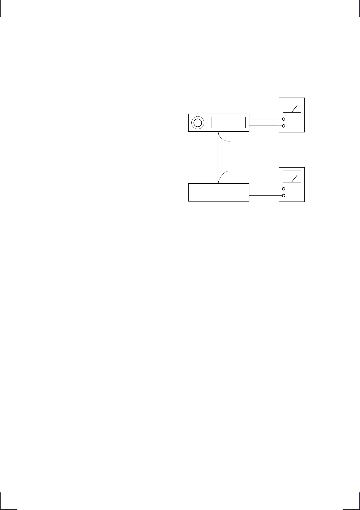
METHOD OF OPERATING THE XDP-4000X
This set cannot be operated alone.
To operated this, it should be connected with a master unit such as
CDX-C880 or XR-C9100 as shown below.
regulated DC
power supply
(14.4V)
master unit
XDP-4000X
BATT,ACC
GND
BUS CONTROL IN
BUS CONTROL IN
(MASTER)
B+
GND
+
–
regulated DC
power supply
(14.4V)
+
–
5. EXPLODED VIEW...........................................................43
6. ELECTRICAL PARTS LIST......................................... 44
– 2 –
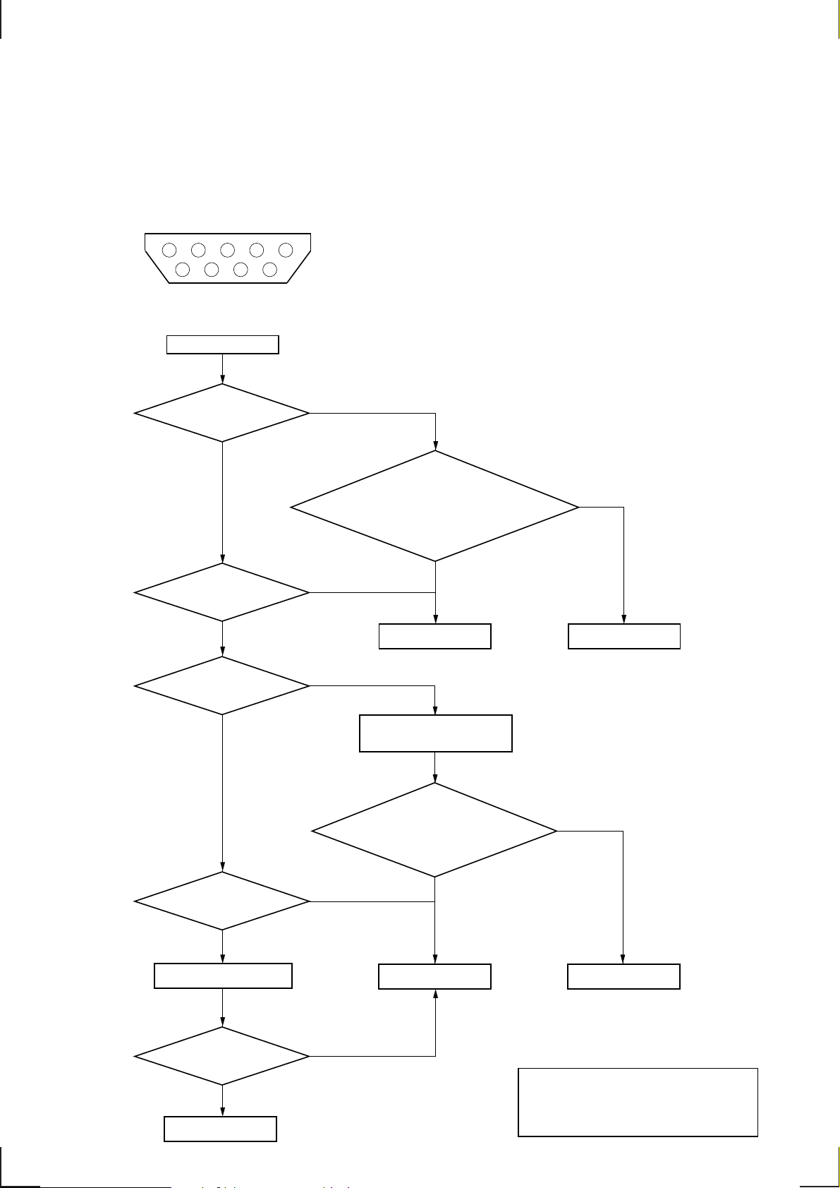
METHOD OF DETERMINING ACCEPTANCE OR REJECTION OF
INTELLIGENCE BOARD (A-3317-137-A) OF XDP-4000X
• No parts in the intelligence board can be repaired.
If the intelligence board is defective, the whole board
should be replaced.
Pin numbers of 9-pin D-SUB connector (CN707)
(viewed from the top of the set)
1 2 3 4 5
6 7 8 9
Note that the voltage given in the following
descriptions is relative to the ground power pin.
Intelligence board check
Is voltage at pin !º of IC707 +5V?
Yes
Is voltage at pin 3 of CN707
between –8 and –9V ?
Yes
Is voltage at pin 9 of IC707 +5V?
Yes
No
Pull cable out of CN703 on main board.
Is voltage at pin 2 of the CN703 +5V?
Yes
No
Intelligence board at fault
No
Set ACC-OFF and pull cable out of
CN703 on main board
No
Main board at fault
Is voltage at pin 2 of CN707 0V?
Yes
Add –8 to –9V to pin 2 of CN707
Is voltage at pin 9 of IC707 0V?
Yes
Intelligence board is normal
Is the resistance between pin 1 of CN703
and ground hundreds of 100 kilohms or more
No
Intelligence board at fault
No
Yes
– 3 –
No
Main board at fault
The fault of the main board may be caused by one of the
following:
1. Shorted CN703 (OPEN).
2. Shorted pins !™ and !¢ of IC702 (OPEN).
3. Damaged port of IC702.
SECTION 2
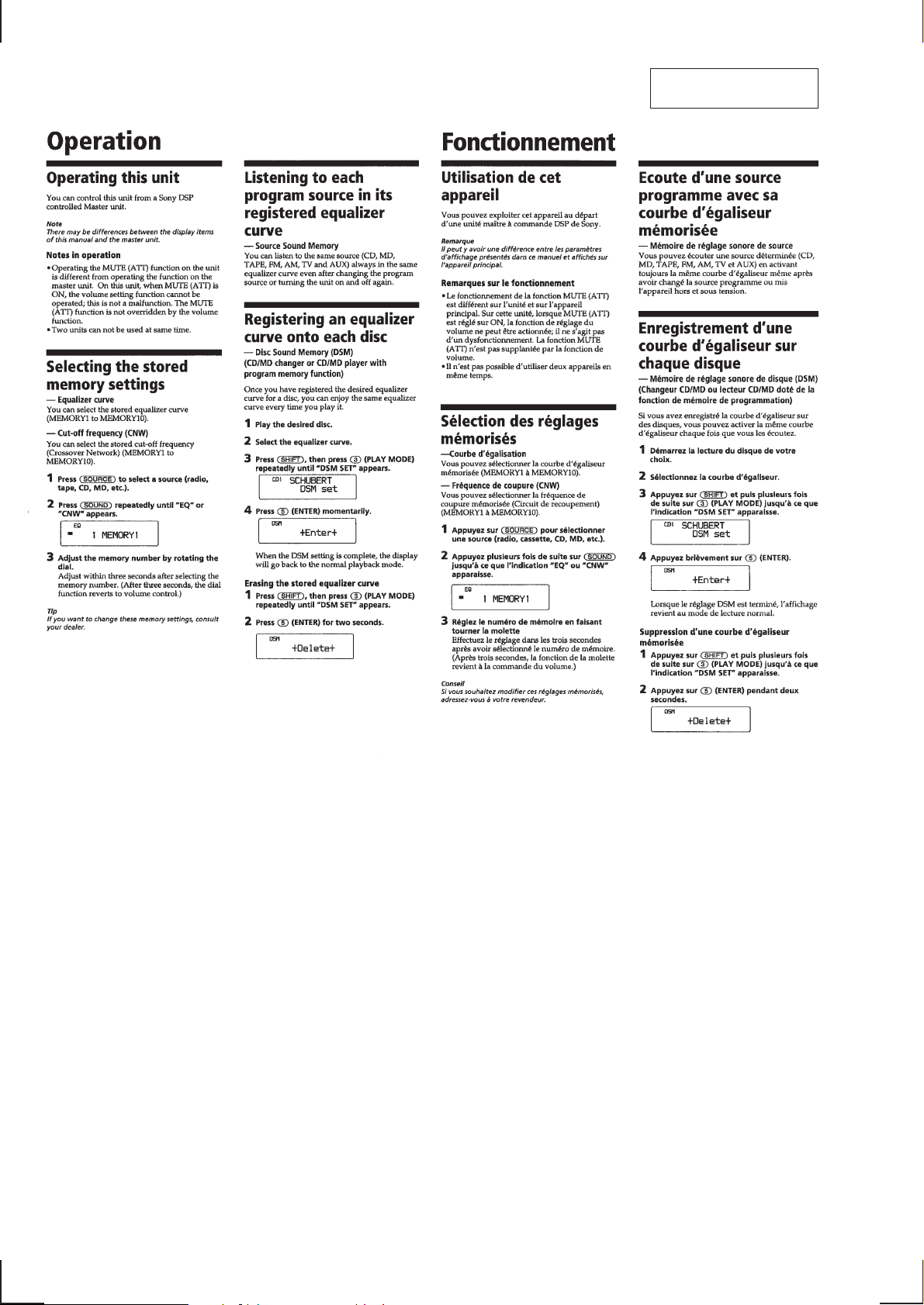
GENERAL
This section is extracted
from instruction manual.
– 4 –
– 5 –
– 6 –
SECTION 3
)
DISASSEMBLY
Note : Follow the disassembly procedure in the numerical order given.
3-1. CASE (UPPER)
1
hexagon socket bolt (M4x6)
7
PTT3x6
3
ornamental plate assy
2
hexagon socket bolt (M4x6
5
CN703
8
PTT3x6
0
case (upper)
3-2. MAIN BOARD
9
PTT3x6
3
PTT3x6
1
connectors
4
CN706
9
spacer
8
2
DAC board
MAIN board
6
PTT3x6
4
PTT3x6
5
PTP3x8
6
PTT2.6x8
– 7 –
7
PTP3x8

SECTION 4
DIAGRAMS
4-1. IC PIN DESCRIPTIONS
• IC502 CXD2710R (DIGITAL SIGNAL PROCESSOR)
Pin No. Pin Name I/O Pin Description
1 AMPIN I Loop filter amplifier input for the PLL.
2 AMPOUT O Loop filter amplifier output for the PLL.
3 VDD — Digital power supply pin (+5 V)
4 VSS — Ground
5 AVSS1 — Ground (for PLL)
6 VCOC I VCO control input
7 AVDD1 — Power supply pin (for PLL) (+5 V)
8 VCOOUT O VCO output for the PLL. Not used. (open)
9 MCK1 I Master clock (768Fs) input
10 MCK2 I Master clock (384Fs) input
11 MCKOUT O Master clock (384Fs) output. Not used. (open)
12 MCKSEL I
13 XMUTE I Output mute signal input of the serial interface. (“L”: mute ON) (Fixed at “H”.)
14 DIN I Program data serial input
15 VSS — Ground
16 SCK I Program data shift clock signal input
17 XLD I Program data load input
18 DOUT O Internal data serial output to the system control (IC702).
19 BUSY O Busy signal at serial data transfer output to the system control (IC702).
20 XCLR I Reset signal input from the system control (IC702). “L”: reset
21 – 27 TEST I Test pin (Normally connect to ground.)
28 VDD — Digital power supply pin (+5 V)
29 VSS — Ground
30 – 38 TEST I Test pin (Normally connect to ground.)
39 TEST — Test pin (Normally open.)
40 VSS — Ground
41 – 52 TEST — Test pin (Normally open.)
53 VDD — Digital power supply pin (+5 V)
54 VSS — Ground
55 – 64 TEST — Test pin (Normally open.)
65 VSS — Ground
66 – 74 TEST — Test pin (Normally open.)
75 EBDIR I Test pin (Normally connect to ground.)
76 UBDIR I Test pin (Normally connect to ground.)
77 TEST0 I Test pin (Normally connect to ground.)
78 VDD — Digital power supply pin (+5 V)
79 VSS — Ground
80 TEST1 I Test pin (Normally connect to ground.)
81 DTEST0 I Test pin (Normally connect to ground.)
82 DTEST1 I Test pin (Normally connect to ground.)
83 AVDD2 — Power supply pin (for D-RAM) (+5 V)
84 AVSS2 — Ground (for D-RAM)
85 AVDD3 — Power supply pin (for D-RAM) (+5 V)
86 AVSS3 — Ground (for D-RAM)
87 S3OUT O Serial data output of 1 sampling, 2 channel.
88 S2OUT O Serial data output of 1 sampling, 2 channel.
89 S1OUT O Serial data output of 1 sampling, 2 channel.
90 VSS — Ground
91 S3DI I Serial data input of 1 sampling, 2 channel.
92 S2DI I Serial data input of 1 sampling, 2 channel.
Input for clock signal setting internal VCO or MCK1 (pin 9).
Internal VCO used: “L”, MCK1 (pin 9) used: “H” (Fixed at “L”.)
– 8 –

Pin No. Pin Name I/O Pin Description
93 S1DI I Serial data input of 1 sampling, 2 channel.
94 BCK I Bit clock input of the serial input/output data.
95 LRCK I Sampling clock input of the serial input/output data.
96 LOCK O Error output of the PLL unlock.
97 V O Frequency divider output for the PLL.
98 VAR I PLL phase comparator variable input
99 REF I PLL phase comparator reference input
100 PD O PLL phase comparator charge pump output
– 9 –
• IC503, 504 CXD2711Q (DIGITAL SIGNAL PROCESSOR)
Pin No. Pin Name I/O Pin Description
1 VSS — Ground
2 CRDY O
3 CCNT I Input of control/data from address bus for the system control (IC702). “L”: data input
4 XCWR I
5 XCRD I Strobe signal input for data reading from the system control (IC702). “L”: data read
6 VDD — Power supply pin (+3.3 V)
7 CD0 I/O Two-way data bus (LSB) with the system control (IC702).
8 CD1 I/O
9 CD2 I/O Two-way data bus with the system control (IC702).
10 CD3 I/O
11 VSS — Ground
12 CD4 I/O
13 CD5 I/O Two-way data bus with the system control (IC702).
14 CD6 I/O
15 CD7 I/O Two-way data bus (MSB) with the system control (IC702).
16 VDD — Power supply pin (+3.3 V)
17 XMUTE I Mute control signal input of the audio data. “L”: mute. (Fixed at “H”.)
18 XCCS I Input of chip select signal from address bus. “L”: chip select
19 VSS — Ground
20 MCKO O Master clock signal (18.432 MHz) output. Not used. (open)
21 VSS — Ground
22 XT2O O System clock signal (36.864 MHz) output. Not used. (open)
23 XT2I I System clock signal (36.864 MHz) input
24 VSS — Ground
25 (BIST) — Test pin. Not used. (open)
26 (TCK) — Test pin. Not used. (open)
27 (TDI) — Test pin. Not used. (open)
28 (TENA1) — Test pin. Not used. (open)
29 (TDO) — Test pin. Not used. (open)
30 VST I Not used. (Fixed at “L”.)
31 VSS — Ground
32 XRST I Reset signal input. “L”: reset
33 BCLK I/O Block clock signal input/output. Not used. (open)
34 LRCK I/O L/R sampling clock signal input/output
35 BCK I/O Bit clock signal input/output
36 VSS — Ground
37 SIA I IC503: Serial audio data signal input from the digital signal processor (IC502).
38 SIB I IC503: Serial audio data signal input from the digital signal processor (IC502).
39 SOA O IC503: Serial audio data (high) signal output
40 SOB O IC503: Serial audio data (high) signal output
41 VSS — Ground
42 – 45 TEST I Test pin. Not used. (Connect to ground.)
Output of ready signal at serial data transfer to the system control (IC702).
“H”: Ready
Strobe signal input for data writing from the system control (IC702).
Data are written by a falling edge.
Serial audio data signal input A
IC504: Serial audio data signal input from the digital signal processor (IC502).
Serial audio data signal input B
IC504: Serial audio data signal input from the digital signal processor (IC502).
Serial audio data signal output A
IC504: Serial audio data (sub) signal output
Serial audio data signal output B
IC504: Serial audio data (low) signal output
– 10 –
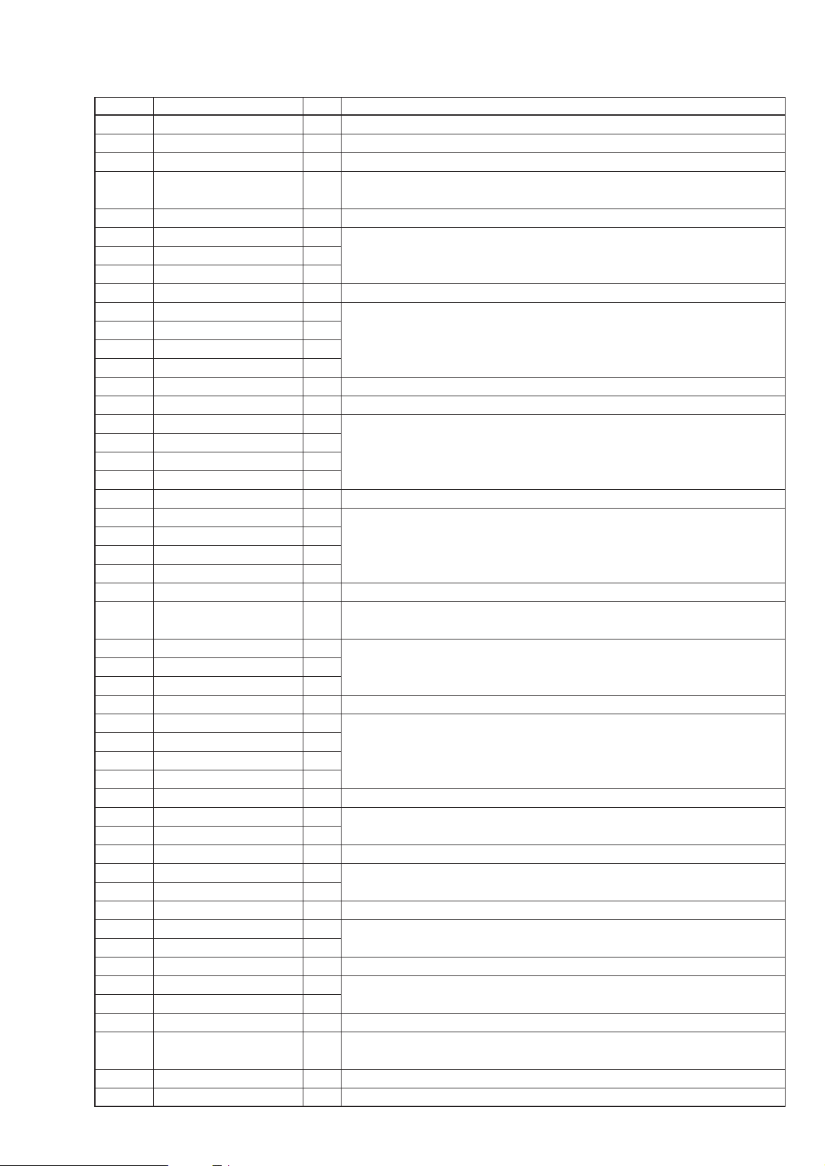
Pin No. Pin Name I/O Pin Description
46 VDD — Power supply pin (+3.3 V)
47, 48 TEST I Test pin. Not used. (Connect to ground.)
49 VSS — Ground
50 MD00 I/O
51 VSS — Ground
52 MD01 I/O
53 MD02 I/O
54 MD03 I/O
55 VSS — Ground
56 MD04 I/O
57 MD05 I/O IC503: External memory data signal input/output to IC512.
58 MD06 I/O IC504: External memory data signal input/output to IC518.
59 MD07 I/O
60 VDD — Power supply pin (+3.3 V)
61 VSS — Ground
62 MD08 I/O
63 MD09 I/O IC503: External memory data signal input/output to IC512.
64 MD10 I/O IC504: External memory data signal input/output to IC518.
65 MD11 I/O
66 VDD — Power supply pin (+3.3 V)
67 MD12 I/O
68 MD13 I/O IC503: External memory data signal input/output to IC512.
69 MD14 I/O IC504: External memory data signal input/output to IC518.
70 MD15 I/O
71 VSS — Ground
72 XRAS O
73 MA09 O
74 MA10 O
75 MA11 O
76 VDD — Power supply pin (+3.3 V)
77 MA12 O
78 MA13 O Row address strobe signal output to external memory (D-RAM) or address signal
79 MA14 O output to external memory (ROM). Not used. (open)
80 MA15 O
81 VSS — Ground
82 MA00 O IC503: Address signal output to external memory (D-RAM: IC512).
83 MA01 O IC504: Address signal output to external memory (D-RAM: IC518).
84 VSS — Ground
85 MA02 O IC503: Address signal output to external memory (D-RAM: IC512).
86 MA03 O IC504: Address signal output to external memory (D-RAM: IC518).
87 VDD — Power supply pin (+3.3 V)
88 MA04 O IC503: Address signal output to external memory (D-RAM: IC512).
89 MA05 O IC504: Address signal output to external memory (D-RAM: IC518).
90, 91 VSS — Ground
92 MA06 O IC503: Address signal output to external memory (D-RAM: IC512).
93 MA07 O IC504: Address signal output to external memory (D-RAM: IC518).
94 VSS — Ground
95 MA08 O
96, 97 MA16, 17 O Address signal output to external memory. Not used. (open)
98 VDD — Power supply pin (+3.3 V)
IC503: External memory data signal input/output to IC512.
IC504: External memory data signal input/output to IC518.
IC503: External memory data signal input/output to IC512.
IC504: External memory data signal input/output to IC518.
IC503: Row address strobe signal output to external memory (D-RAM: IC512).
IC504: Row address strobe signal output to external memory (D-RAM: IC518).
Row address strobe signal output to external memory (D-RAM) or address signal
output to external memory (ROM). Not used. (open)
IC503: Address signal output to external memory (D-RAM: IC512).
IC504: Address signal output to external memory (D-RAM: IC518).
– 11 –
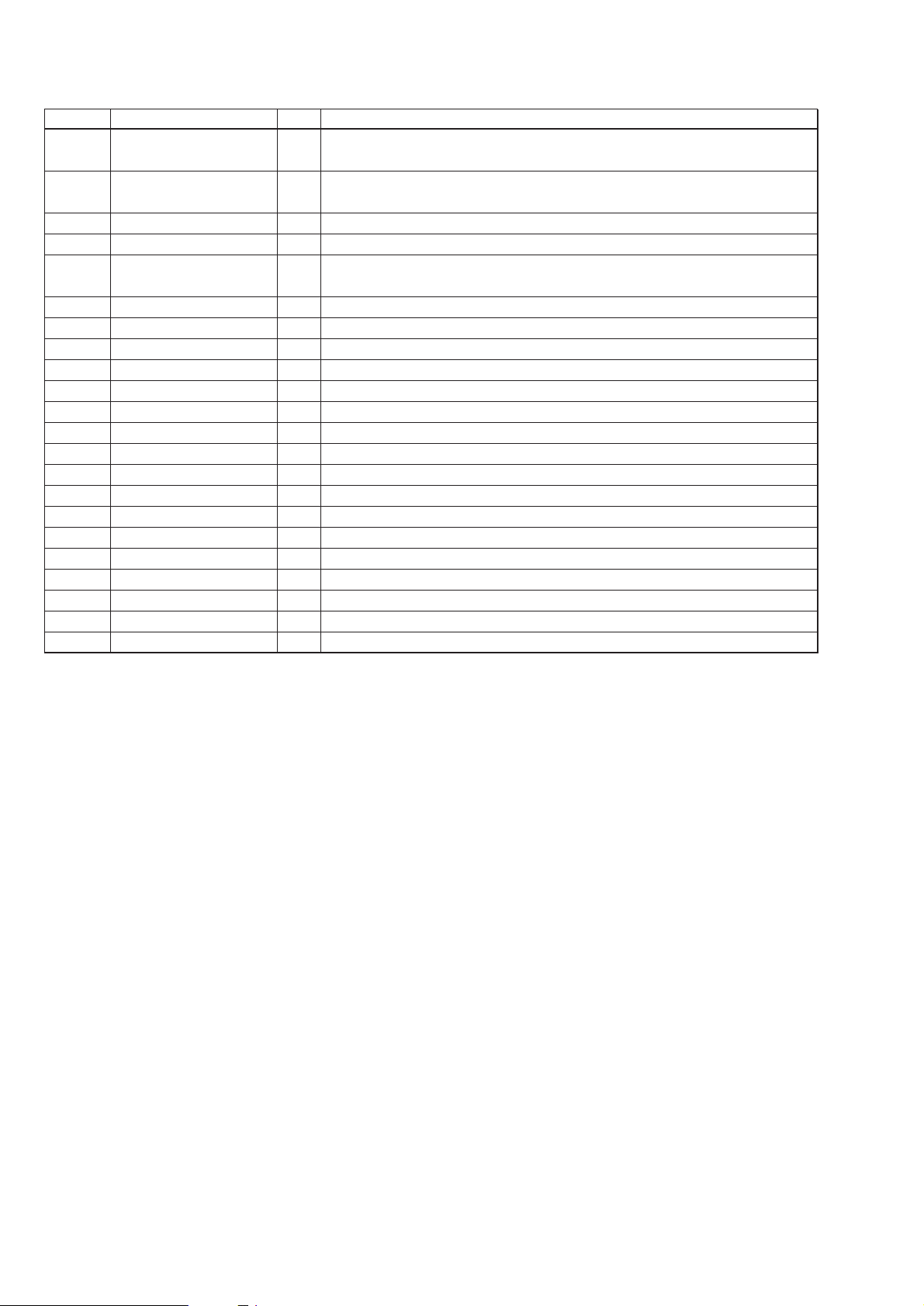
Pin No. Pin Name I/O Pin Description
99 XMUTE O
100 XMODE O
101 VSS — Ground
102 XMCS O Chip select output to external memory (ROM). Not used. (open)
103 XCAS O
104 VSS — Ground
105 DEND O Internal operation monitor signal output (DMU END). Not used. (open)
106 VDD — Power supply pin (+3.3 V)
107 PEND O Internal operation monitor signal output (PROC END). Not used. (open)
108 ENC0 O Internal operation monitor signal output (BUS ENC0). Not used. (open)
109 ENC1 O Internal operation monitor signal output (BUS ENC1). Not used. (open)
110 ENC2 O Internal operation monitor signal output (BUS ENC2). Not used. (open)
111 VSS — Ground
112 STOP O Internal operation monitor signal output (BUS STOP). Not used. (open)
113 HOLD O Internal operation monitor signal output (BUS HOLD). Not used. (open)
114 OVF O Overflow signal output at the operation. “H”: overflow. Not used. (open)
115 LIM O Fixed/float conversion limiter signal output. “H”: limiter on. Not used. (open)
116 BTIA I Bit signal input A
117 BTIB I Bit signal input B
118 BTOA O Bit signal output A. Not used. (open)
119 BTOB O Bit signal output B. Not used. (open)
120 VDD — Power supply pin (+3.3 V)
IC503: Write enable signal output to external memory (D-RAM: IC512).
IC504: Write enable signal output to external memory (D-RAM: IC518).
IC503: Output enable signal output to external memory (D-RAM: IC512).
IC504: Output enable signal output to external memory (D-RAM: IC518).
IC503: Column address strobe signal output to external memory (D-RAM: IC512).
IC504: Column address strobe signal output to external memory (D-RAM: IC518).
– 12 –
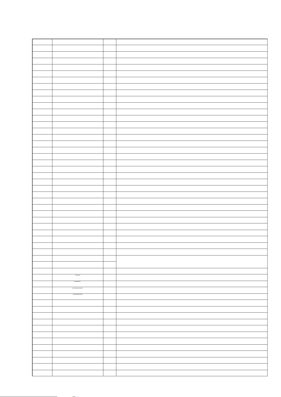
• IC702 HD6473048SF16 (SYSTEM CONTROL)
Pin No. Pin Name I/O Pin Description
1 VCC — Power supply pin (+5 V)
2 DSPON O System, digital, analog and amplifier remote power supply control signal output.
3 SOUT O Serial data signal output
4 SCKO O Serial clock signal output
5 VCE0 O Not used. (open)
6 2710CE O Program data load output to digatal signal processor (IC502).
7 EE-CKO O Connect to SCK pin of EEPROM (IC705).
8 SP-CE O Serial /Parallel chip enable signal output
9 DSPRDY I Data transfer ready signal input
10 VPP — Not used. (Connect to ground.)
11 VSS — Ground
12 EXT/IO (TX) O UART serial data signal output
13 UNISO O Bus serial data signal output
14 EXT/IO (RX) I UART serial data signal input
15 UNISI I Bus serial data signal input
16 DSPRST O DSP reset control signal output
17 UNICKI I Bus clock signal input
18 – 21 D0 – 3 I/O Two-way data bus to external device. H: Bus off, Back up off.
22 VSS — Ground
23 – 34 D4 – 15 I/O Two-way data bus to external device. H: Bus off, Back up off.
35 VDD — Power supply pin (+5 V)
36 – 43 A0 – 7 O Address bus signal output to external device. H: Bus off, Back up off.
44 VSS — Ground
45 – 56 A8 – 19 O Address bus signal output to external device. H: Bus off, Back up off.
57 VSS — Ground
58 AMUTE O Mute control signal output (Relay mute control)
59 MUT/PW O Mute power signal output
60 — — De-emphasis control signal output. Not used. (open)
61 NC — System clock signal output to external device. Not used. (open)
62 STBY I Hardware standby signal input. Fixed at “H”. (Connect to VDD.)
63 SYSRESET I Reset signal input
64 BU-IN I Back up detect signal input
65 VSS — Ground
66 X-IN I
67 EX-IN I
68 VDD — Power supply pin (+5 V)
69 AS — Address strobe signal output. Not used. (open)
70 RD O Read signal output
71 HWR O High write signal output
72 LWR O Low write signal output
73 MD0 I Operation mode control signal input. Fixed at “L”. (Connect to ground.)
74, 75 MD1, 2 I Operation mode control signal input. Fixed at “H”. (Connect to VDD.)
76 AVDD — Power supply pin (+5 V)
77 AVREF I Reference voltage signal input
78 DSPBU I DSP BU signal input
79 LOCK (2710) I PLL unlock error detect signal input from digital signal processor (IC502).
80 — — Not used. (Connect to ground.)
81 VOLMAX I Not used. (Connect to ground.)
82 DSPBUSY I Busy signal input
83 SDI-AGC I AGC out signal input. Not used. (Connect to ground.)
84 BU-IN I Back up detect signal input
85 DSPSI (2710) I Data signal input from digital signal processor (IC502).
Oscillator (14.7456 MHz) connect pin
– 13 –
 Loading...