

Sony XA43M61, XA43M91, KP-XA43M61, KP-XA43M91 Service Manual
HISTORY
Model Name : KP-XA43M31/
XA43M61/XA43M91
SERVICE MANUAL
When clicking an item, it’s detail is displayed. Parts No. : 9-965-428-01
Date SUP/COR No. Description of SUP/COR
2001.6 NEW YES
Change of
main text
SERVICE MANUAL
MODEL COMMANDER DEST. CHASSIS NO.
MODEL COMMANDER DEST. CHASSIS NO.
CHASSIS
RG-2
PROJECTION TV
KP-XA43M31 RM-967 AUS SCC-N73J-A
KP-XA43M61 RM-967 GE SCC-N69L-A
KP-XA43M91 RM-967 ME SCC-N72J-A
KP-XA43M31/XA43M61/XA43M91
RM-967

– 2 –
KP-XA43M31/XA43M61/XA43M91
RM-967
CAUTION
SHORT CIRCUIT THE ANODE OF HTE PICTURE TUBE
AND THE ANODE CAP TO THE METAL CHASSIS, CRT
SHIELD, OR CARBON PAINTED ON THE CRT, AFTER
REMOVING THE ANODE.
SAFETY-RELATED COMPONENT WARNING!!
COMPONENTS IDENTIFIED BY SHADING AND MARK
! ON THE SCHEMATIC DIAGRAMS, EXPLODED
VIEWS AND IN THE PARTS LIST ARE CRITICAL TO
SAFE OPERATION. REPLACE THESE COMPONENTS
WITH SONY PARTS WHOSE PART NUMBERS APPEAR AS SHOWN IN THIS MANUAL OR IN SUPPLEMENTS PUBLISHED BY SONY.
SPECIFICATIONS
Projection system 3 picture tubes, 3 lenses,
horizontal in-line system
Picture tube 7 inch high-brightness
monochrome tubes (6.3 raster
size), with optical coupling and
liquidcooling system
Projection lenses High performance, large-diameter
hybrid lens F1.0
Screen size 43 inches
Television system B/G, I, D/K, M
Color system PAL, PAL 60, SECAM,
NTSC
4.43, NTSC3.58
Channel coverage B/G
VHF: E2 to E12
UHF: E21 to E69
CATV: S01 to S03, S1 to S41
I
UHF: B21 to B68
CATV: S01 to S03, S1 to S41
D/K
VHF: C1 to C12, R1 to R12
UHF: C13 to C57, R21 to R60
CATV: Z1 to Z39, S01 to S03,
S1 to S41
M
VHF: A2 to A13
UHF: A14 to A79
CATV: A-8 to A-2, A to W+4,
W+6 to W+84
Stereo system NICAM stereo B/G, I, D/K
A2 stereo (German) B/G
Antenna 75 ohm external antenna terminal
Audio output
(Speaker) 15 W x 2
Number of terminals
Video Input: 4, Output: 1,
phono jacks, 1 Vp-p, 75 ohms
Audio Input: 5, Output: 1,
VARIABLE output: 1,
phono jacks, 500 mVrms
S video Input: 2,
Y:1 Vp-p, 75 ohms, unbalanced,
sync negative,
C:0.286 Vp-p, 75 ohms
Component video Input: 1, phono jacks
Y:1.0 Vp-p, 75 ohms, sync negative
C
B/B-Y: 0.7 Vp-p, 75 ohms
C
R/R-Y: 0.7 Vp-p, 75 ohms
Audio: 500 mVrms
Headphone Output: 1,minijack
Power requirement 110-240 V AC, 50/60 Hz
Power consumption 160 W
Dimensions (w/h/d) 966 x 1,074 x 505 mm
Mass Approx. 60 kg
Supplied accessories Remote commander RM-967 (1)
Size R6 (AA) battery (2)
Optional accessories TV stand SU-XA43
Design and specifications are subject to change without notice.

– 3 –
KP-XA43M31/XA43M61/XA43M91
RM-967
1. GENERAL ................................................................. 4
2. DISASSEMBLY
2-1. Rear Board Removal ......................................... 17
2-2. Main Bracket Section Removal ........................ 17
2-3. Service Position ................................................. 17
2-4. H1, H2 Boards and Resistor
(High Voltage) Removal ................................... 17
2-5. Beznet Section Removal ................................... 18
2-6. G Board Removal ............................................... 18
2-7. P1 Board and V2 Board Removal ...................... 18
2-8. UG Board, AG Board and S Board Removal .... 19
2-9. Chassis Block Removal ...................................... 19
(1) H1, H2 Boards and Resistor Removal .............. 19
(2) Main Bracket Removal ...................................... 20
(3) Chassis Block Removal ..................................... 20
2-10. High-Voltage Cable Installation and Removal.. 21
2-11. Mechasel Assy Removal .................................... 21
3. SET-UP ADJUSTMENTS
3-1. Screen Voltage Adjustment
(Rough Alignment) ........................................... 22
3-2. Focus Adjustment .............................................. 22
3-3. Screen (G2) Adjustment .................................... 22
3-4. Deflection Yoke Tilt Adjustment ...................... 22
3-5. 2-Pole Magnet Adjustment ................................ 23
3-6. 4-Pole Magnet Adjustment ................................ 23
3-7. Defocus Adjustment (Blue) ............................... 23
3-8. Green and Red Focus Adjustment ..................... 23
3-8-1. Green and Red Lens Focus Adjustment ....... 23
3-8-2. Green and Red Electrical Focus
Adjustment .................................................... 23
4. SAFETY RELATED ADJUSTMENT
4-1. HV Hold Down Adjustment ............................. 24
5. CIRCUIT ADJUSTMENTS
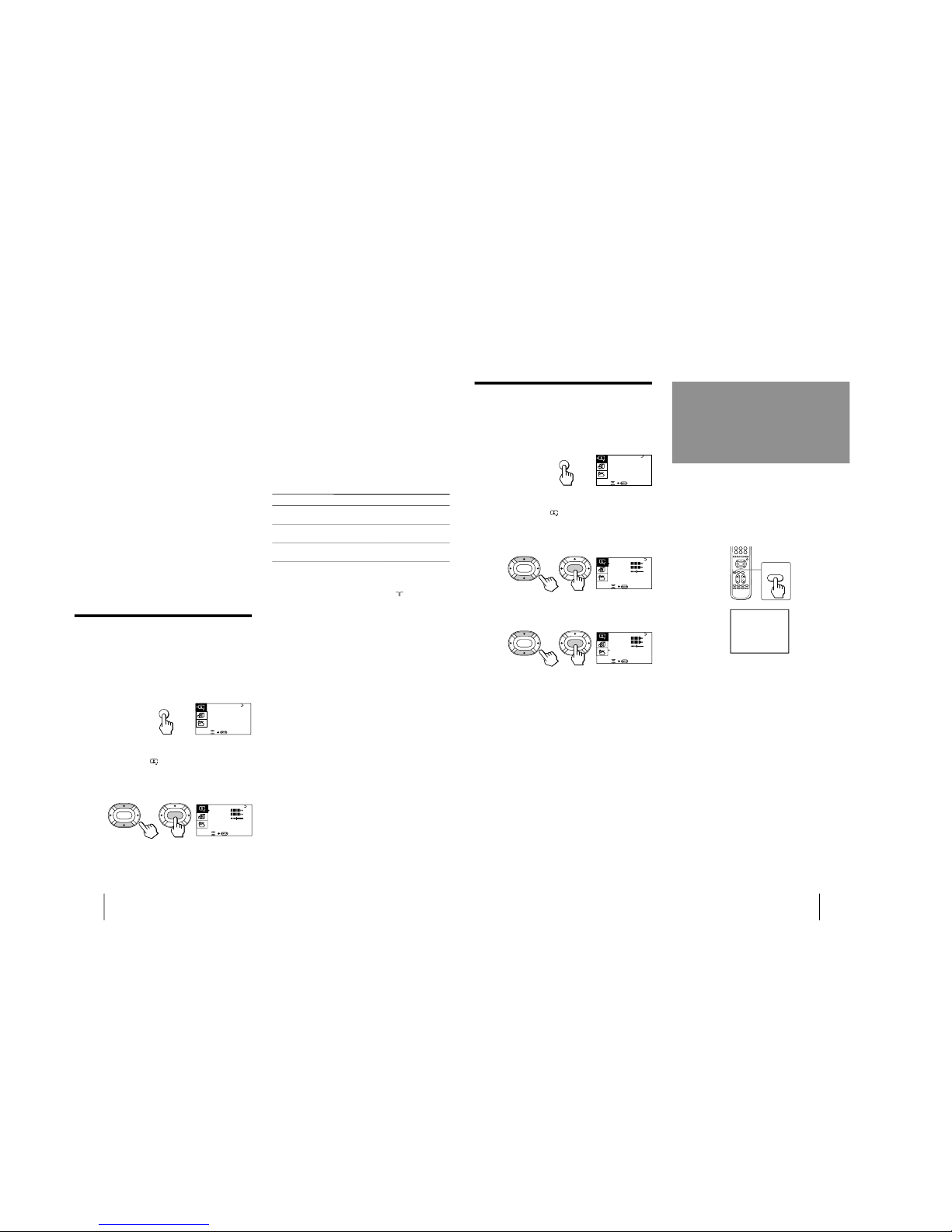
5-1. Adjustments with Commander ......................... 25
5-2. Adjustment Method ........................................... 26
5-3. Adjustment After IC1001 and IC1702
Replacement ....................................................... 26
5-4. Registration (Convergence)Adjustment
Method ................................................................ 33
5-5. Auto Convergence Adjustment .......................... 38
5-6. White Balance Adjustment ................................ 39
5-7. Text Position Adjustment ................................... 39
5-8. Picture Quality Adjustments ............................. 39
TABLE OF CONTENTS
6. DIAGRAMS
6-1. Block Diagrams .................................................. 40
6-2. Frame Schematic Diagram ................................. 46
6-3. Circuit Boards Location ..................................... 47
6-4. Schematic Diagrams and Printed Wiring
Boards ................................................................. 47
(1) Schematic Diagram of AG (1/5) Board ............. 48
(2) Schematic Diagram of AG (2/5) Board ............ 49
(3) Schematic Diagrams of AG (3/5) Board ........... 50
(4) Schematic Diagram of AG (4/5) Board ............. 51
(5) Schematic Diagram of AG (5/5) Board ............ 52
(6) Schematic Diagrams of CR Board ..................... 57
(7) Schematic Diagram of CG Board ...................... 58
(8) Schematic Diagram of CB Board ..................... 59
(9) Schematic Diagrams of D(1/3) Board ............... 60
(10) Schematic Diagrams of D(2/3) Board ............... 61
(11) Schematic Diagrams of D(3/3) Board ............... 62
(12) Schematic Diagram of E (1/4) Board ................ 66
(13) Schematic Diagram of E (2/4) Board ............... 67
(14) Schematic Diagrams of E (3/4) Board ............... 68
(15) Schematic Diagram of E (4/4) Board ................ 69
(16) Schematic Diagram of G (1/2) Board ............... 72
(17) Schematic Diagrams of G(2/2) Board ............... 73
(18) Schematic Diagram of H1 Board ....................... 76
(19) Schematic Diagram of H2 Board ...................... 77
(20) Schematic Diagrams of P1 Board ...................... 78
(21) Schematic Diagrams of S Board ........................ 81
(22) Schematic Diagrams of UG Board .................... 83
(23) Schematic Diagram of V2 Board ....................... 84
(24) Schematic Diagram of ZR Board ...................... 85
(25) Schematic Diagrams of ZG Board ..................... 86
6-5. Semiconductors ................................................. 87
7. EXPLODED VIEWS
7-1. Screen and Cover Block ................................... 88
7-2. Cabinet and Panel Block .................................. 89
7-3. Chassis and Picture Tube Block ........................ 90
8. ELECTRICAL PARTS LIST ............................ 91
Section Title PageSection Title Page
– 4 –
KP-XA43M31/XA43M61/XA43M91
RM-967
SECTION1
GENERAL
The operating instructions mentioned here are partial abstracts
from the Operating Instruction Manual. The page numbers of the
Operating Instruction Manual remein as in the manual.
6
-EN
Getting Started
1
L
(MONO)
R
2
3
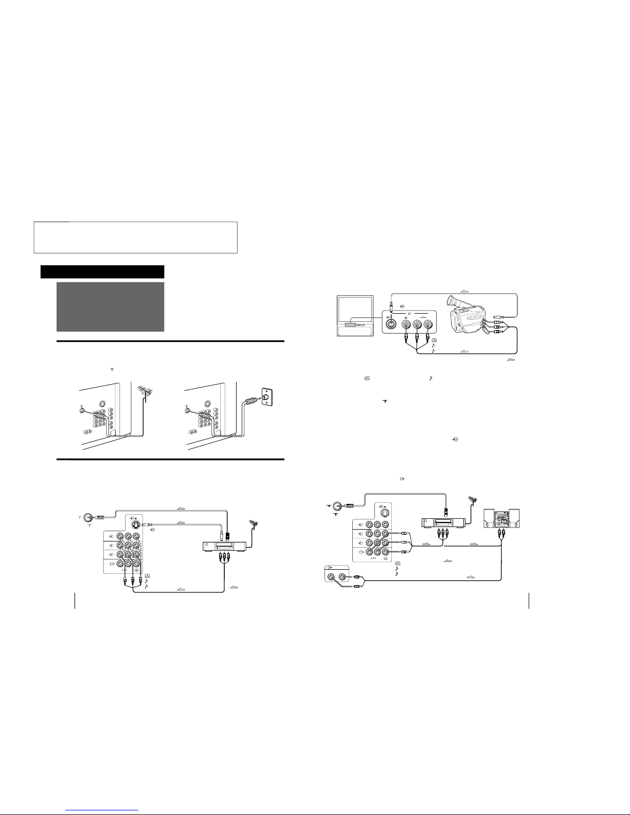
Connections
On a wall
Rear of TV
Rear of TV
or
Rear of TV
VCR
to
S video
output
to
antenna
output
to video and
audio outputs
: Signal flow
Getting Started
to
(antenna) socket
to
…
1, 2, or 3 (video input)
(yellow)
-L (MONO)(white)
-R (red)
to
(S video input)
Connecting a VHF antenna or a combination VHF/UHF antenna
— 75-ohm coaxial cable (round)
Attach an optional IEC antenna connector to the 75-ohm coaxial cable.
Plug the connector into the
(antenna) socket at the rear of the TV.
Connecting optional equipment
You can connect optional audio/video equipment to your TV such as a VCR, multi disc player, camcorder, video
game or stereo system.
Connecting video equipment using video input jacks
7
-EN
Getting Started
L( MONO)
R
3
1
L
(MONO)
R
2
3
(VARIABLE)
RL
Camcorder
to S video output
to video and
audio outputs
: Signal flow
Rear of TV
VCR
to
antenna
output
to video and
audio inputs
Audio system
to audio
inputs
: Signal flow
or
to
(S video input)
to
…
3 (video input)
(yellow)
-L (MONO)(white)
-R (red)
to
(antenna) socket
to
Ú
(monitor/TV output)
(yellow)
-L (MONO)(white)
-R (red)
When connecting a monaural VCR
Connect the yellow plug to
(video input) and the black plug to
-L (MONO) (audio input).
When connecting video game equipment
Connect video game equipment to the … 3 (video input) jacks at the front or the rear of your TV.
When connecting a VCR to the
(antenna) terminal
Preset the signal output from the VCR to the program position 0.
When connecting video equipment to the … 3 (video input) jacks at the front and the rear
Do not connect video equipment to the … 3 (video input) jacks at the front and the rear of your TV simultaneously; otherwise the picture
will not be displayed properly on the screen.
If both S Video and video signals are input simultaneously
The S video input signal is selected. To view a video input signal, disconnect the
(S video) connection.
Note on the video input
When no signal is input, the screen becomes blue.
Connecting audio/video equipment using Ú (monitor/TV output) jacks
When the audio cable is connected to the
(VARIABLE) jacks, you can adjust the volume with Á +/–.
Front of TV
– 5 –
KP-XA43M31/XA43M61/XA43M91
RM-967
8
-EN
Getting Started
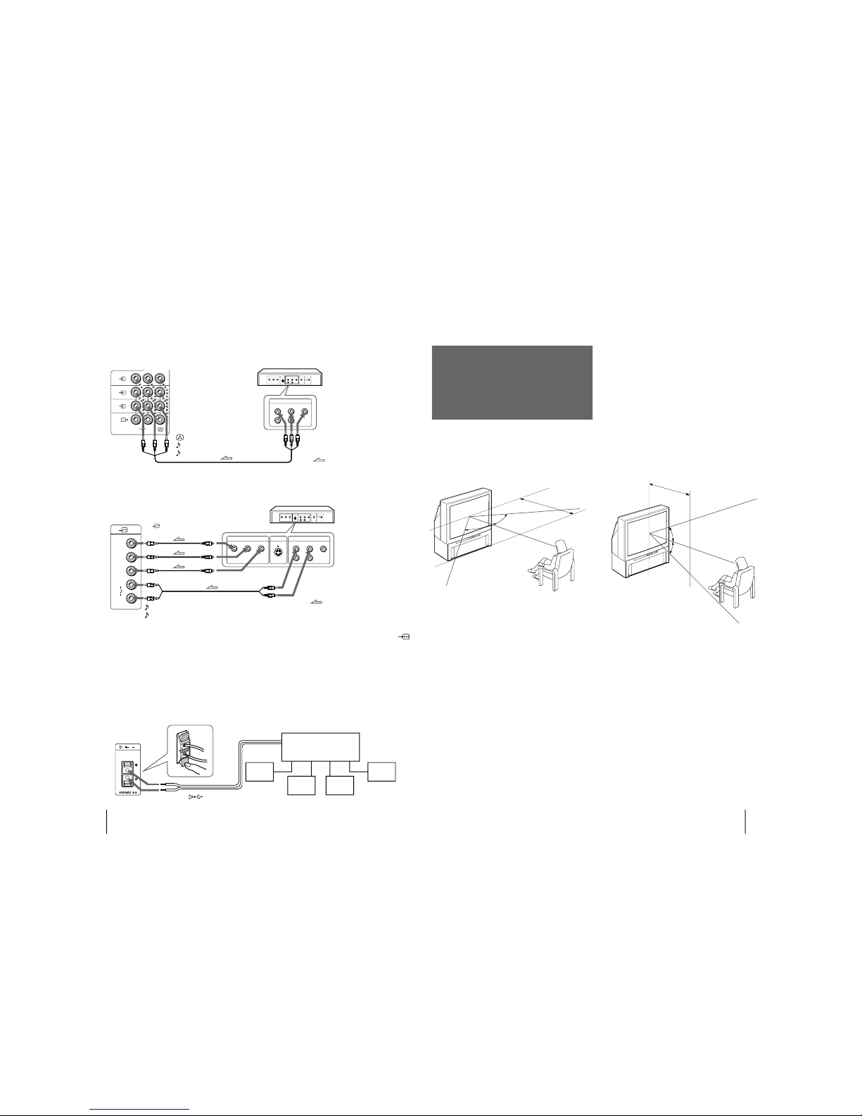
COMPOMENT VIDEO OUT
S VIDEO OUT
LINE OUT
C
B
/B-YYC
R
/R-Y
R-AUDIO-L VIDEO
C
R
/
R-Y
C
B
/
B-Y
Y
L
R
1
L
(MONO)
R
2
3
LINE OUT
R-AUDIO-L VIDEO
Connecting a DVD player
C
Connecting an amplifier with Dolby* Pro Logic decoder
Even though you use an amplifier with Dolby Pro Logic
decoder instead of the projection TV
’s audio system, you
can still use the projection TV
’s center speaker.
* Manufactured under license from Dolby Laboratories
Licensing Corporation.
DOLBY, the double-D symbol a and “PRO LOGIC” are
trademarks of Dolby Laboratories Licensing Corporation.
Amplifier with Dolby Pro
Logic decoder
Rear
speaker
(L)
Rear
speaker
(R)
Front
speaker
(L)
Front
speaker
(R)
to
(center speaker
inputs)
Rear of TV
Connecting a DVD player with component video output connectors
Notes
• Since the high quality pictures on a DVD disc contain a lot of
information, picture noise may appear. In this case, adjust the
sharpness (SHARP) in the VIDEO ADJUST menu. (See page 19.)
• Connect your DVD player directly to your TV. Connecting the
DVD player through other video equipment will cause unwanted
picture noise.
• If your DVD player can output interlace and progressive mode
signals, select the interlace output when connecting to
(component video input) on your TV.
Your TV can receive either 525i/60 Hz or 625i/50 Hz interlace
signals.
Rear of TV
: Signal flow
to audio/
video
outputs
DVD player
to
…
1, 2, or 3 (video input)
(yellow)
-L (MONO)(white)
-R (red)
Rear of TV
: Signal flow
-L (white)
-R (red)
to
(component video
input) Y/C
B
/B-Y/C
R
/R-Y
to component video
output
to audio output
DVD player
9
-EN
Getting Started
Installing the
projection TV
min 1.5m (5 ft.)
75°
75°
Optimum viewing area (Vertical)
min 1.5m (5 ft.)
27°
27°
For the best picture quality, install the projection TV
within the areas shown below.
Optimum viewing area (Horizontal)

– 6 –
KP-XA43M31/XA43M61/XA43M91
RM-967
10
-EN
Getting Started
PROGR
MENU
A/B
GAME
1
2
3
4
5
6
7
8
0
-/--
9
ENTER
POWER
BASSO
1
2
3
4
!§
5
6
7
!¶
!•
!ª
!∞
!¢
!£
!™
!¡
!º
9
8
TITLE
VIDEO
Symbol
1
2 ¤
3 A/B
4
5 ÷
6 POWER
BASSO
7 .+/–
8 GAME
9 u
!º …
!¡ ;
!™ 1,2,3,4,5,
6,7,8,9,0
!£ JUMP
!¢ MENU
!∞ V/b/v/B
ENTER
!§ ©
!¶
!• PROGR +/–
!ª
VIDEO u
+/#
(
=/3
p
P
r
TITLE
Names/symbols of buttons on the remote commander are indicated in different colors to represent the available
functions.
Label color Button function
White For general TV operations.
Green For Teletext operations.
Getting to know the
remote commander
Name Refer to page
On-screen display button 18
Teletext: Reveal button 25
Mute on/off button 18
Sound select button 23
Teletext: Enlarge button 25
Teletext button 24
Double-digit entering button 17
POWER BASSO button 21
Volume control button 17
GAME button 25
TV standby button 17
Input mode selector 18
Hold button 24
TV power on/TV mode selector 18
Number buttons 17
JUMP button 18
MENU button 11
Cursor control key 11
Enter button 11
Teletext: INDEX button 24
Sleep timer button 18
Teletext: Text clear button 25
Program selectors 17
DVD, VCR, MDP, CD, MD 25
operation buttons
Power button 25
Fastforward/search forward 26
button
Play button 26
Rewind/search backward 26
button
Stop button 26
Pause button 26
Record button 26
TITLE button 26
11
-EN
Getting Started
A / V CONTROL
DYNAMIC
SOFT
STANDARD
PERSONAL
V IDEO AD JUST
AUDI O AD JUST
TV SYS: B /G
VHF
LO
W
PR: 01
AT T : OFF
MANUAL PROGRAM
VOLUME: 0
TV SYS: B /G
AUTO PROGRAM
VHF LO
W
PR: 01
PRESET
SKI P:
PR02 OFF
TV SYS: B /G
COL
SYS :AUTO
ENGL I SH
AUTO PROGRAM
MANUAL PROGRAM
LA NGUAGE/
:
GAME MODE
HYPER SURROUND :
OFF
MONITOR
AV OUT:
FEATURES
CONVERGENCE
BASS
80
00
80
TREBLE
BAL ANCE
AUDI O AD JUST
SPEAKER:
MAIN
P IC TURE
50
90
0
50
V IDEO ADJ UST
COLOR
BR I GHT
HUE
SHARP
VM: H IG H
50
0
A/V CONTROL
FEATURES
Getting back to the previous menu
(except for AUTO PROGRAM)
Press V or v to move the cursor (z) to the first
line (N) of each menu, and press ENTER.
Cancelling the menu screen
Press MENU.
Notes (except for AUTO PROGRAM)
• When a menu is selected after pressing ENTER, the color of
both the menu and the menu symbol change and the cursor
(z) appears beside the first item of the menu.
• When an item on the menu is selected after pressing ENTER,
the color of the item changes.
• You can refer to the guide (
) at the bottom of the
menus (except for the and PRESET menu) for the basic
operations of the menu.
• If more than approximately 60 seconds elapse after you press a
button, the menu screen disappears automatically.
PRESET
Introducing the
menu system
You can preset TV channels, adjust the picture and sound qualities, and select some settings using the on-screen
menus. You can use the buttons on both the remote commander and the TV to operate the menus.
– 7 –
KP-XA43M31/XA43M61/XA43M91
RM-967
12
-EN
Getting Started
A / V CONTROL
DYNAM IC
SOFT
STANDARD
PERSONAL
VI DEO ADJ UST
AUDI O AD JUST
MENU
MENU
ENTER
PRESET
SKIP: PR02 OFF
TV SYS: B /G
COL SYS: AUTO
ENGL I SH
AUTO PROGRAM
MANUAL PROGRAM
LANGUA GE/
:
ENTER
ENTER
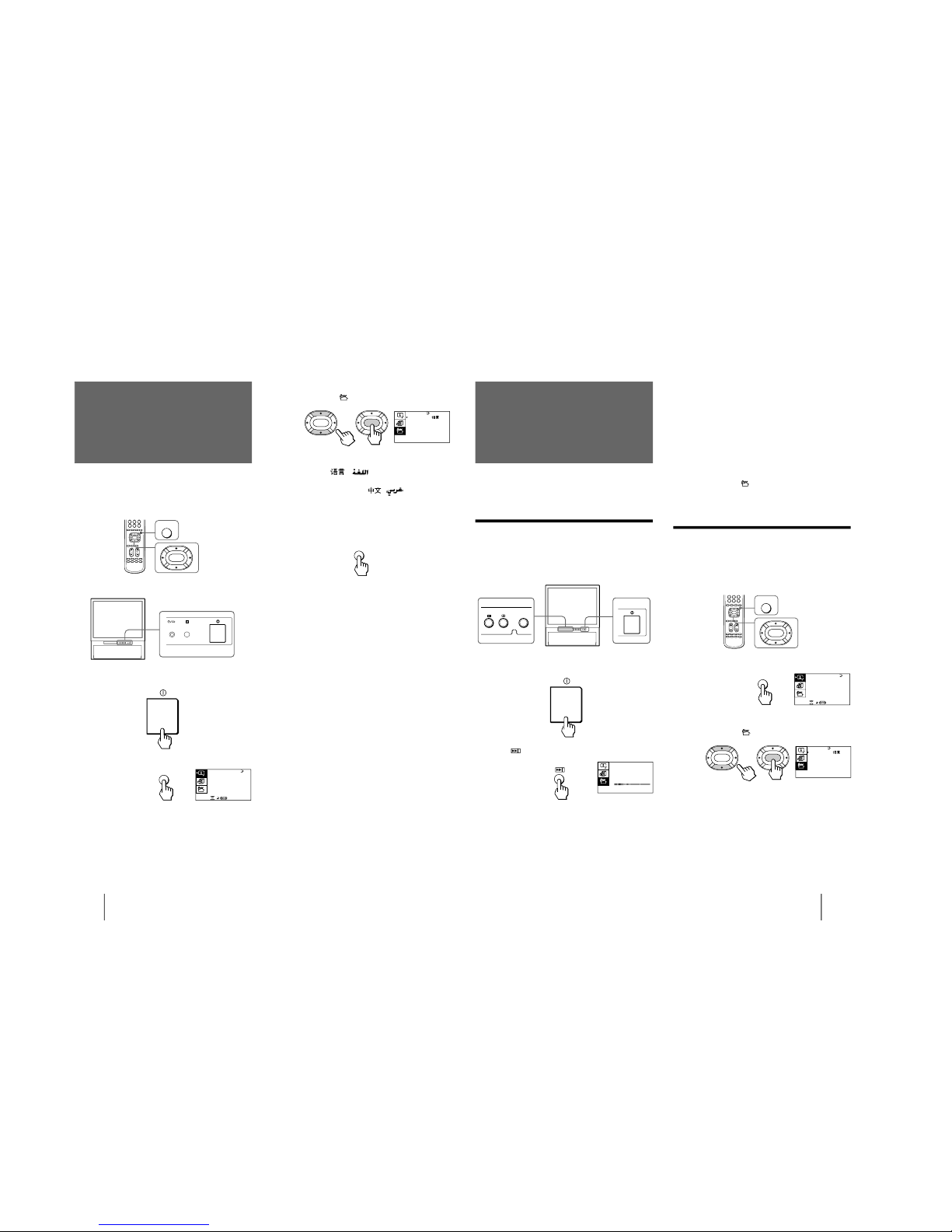
Changing the menu
language
If you prefer Chinese (for M61/M31 model)/Arabic
(for M91 model) to English, you can change the menu
language. You can use buttons on both the remote
commander and the TV.
1
Press U to turn on the TV.
2
Press MENU.
3
Press V or v to move the cursor (z) to the
PRESET menu (
), and press ENTER.
4
Make sure the cursor (z) appears beside
LANGUAGE/
(
), and press ENTER.
5
Press V/b/v/B to select
(
), and press
ENTER.
All of the menus change to Chinese (Arabic).
6
Press MENU to return to the normal screen.
MENU
13
-EN
Getting Started
You can preset TV channels easily by storing all the
receivable channels automatically. You can also preset
channels manually or disable program positions (see
page 15 ).
Presetting channels automatically
You can preset up to 100 TV channels in numerical
sequence from the program position 1. You can preset
channels automatically using the button on the TV or
the menu.
1
Press U to turn on the TV.
2
Press
.
The TV starts scanning and presetting channels
automatically. When all of the receivable channels
are stored, the AUTO PROGRAM menu
disappears.
MENU
ENTER
PRESET
SKIP: PR02 OFF
TV SYS: B /G
COL SYS : AUTO
ENGL I SH
AUTO PROGRAM
MANUAL PROGRAM
LANGUA GE/
:
ENTER
ENTER
Presetting channels
TV SYS:B /G
AUTO PROGRAM
VHF LO
W
PR: 01
A / V CONTROL
DYNAM IC
SOFT
STANDARD
PERSONAL
V ID EO ADJ UST
AUDI O AD JUST
MENU
Note
• If you want to return to the normal screen while the nine sub
screens are being displayed, you can press PROGR INDEX on
the remote commander.
To preset channels automatically using
the menu
1 Press MENU.
2 Press V or v to move the cursor (z) to the
PRESET menu (
), and press ENTER.
3 Press V or v to move the cursor (z) to AUTO
PROGRAM, and press ENTER.
Presetting channels manually
To change the program position for a channel or to
receive a channel with a weak signal which you cannot
receive by automatic presetting, preset the channel
manually.
1
Press MENU.
2
Press V or v to move the cursor (z) to the
PRESET menu (
), and press ENTER.
3
Select your local TV system.
(1) Press V or v to move the cursor (z) to TV SYS, and
press ENTER.
(2) Press V/b/v/B until your local TV system appears
on the menu, and press ENTER.
ENTER
– 8 –
KP-XA43M31/XA43M61/XA43M91
RM-967
14
-EN
Getting Started
TV SYS:B /G
VHF
LO
W
PR: 01
ATT : OFF
MANUAL PROGRAM
ENTER
ENTER
VOLUME: 0
TV SYS:B/G
VHF
LO
W
PR: 01
ATT: OFF
MANUAL PROGRAM
ENTER
ENTER
VOLUME: 0
PRESET
SKIP: PR02 OFF
TV SYS: B /G
COL SYS: AUTO
ENGL I SH
AUTO PROGRAM
MANUAL PROGRAM
LANGUAGE/
:
ENTER
ENTER
TV SYS:B/G
VHF
LO
W
PR: 01
ATT : OFF
MANUAL PROGRAM
ENTER
ENTER
VOLUME: 0
4
Press V or v to move the cursor (z) to
MANUAL PROGRAM, and press ENTER.
5
Select the program position to which you
want to preset a channel.
(1) Make sure the cursor (z) appears beside PR, and
press ENTER.
(2) Press V/b/v/B until the program position you
want appears on the menu, and press ENTER.
6
Select the desired channel.
(1) Press V or v to move the cursor (z) to VHF LOW
(VHF Hi or UHF), and press ENTER.
(2) Press V/b/v/B until the desired channel picture
appears on the TV screen, and press ENTER.
7
Press MENU to return to the normal screen.
If the TV system is not properly selected
The picture color may be poor and/or the sound may
be noisy. In this case, select the appropriate TV system.
1 Press PROGR +/
– or the number buttons to select
the program position.
2 Display the PRESET menu.
3 Press V or v to move the cursor (z) to TV SYS, and
press ENTER.
4 Press V/b/v/B until the appropriate TV system
appears, and press ENTER.
Notes
• The TV SYS (TV system), the ATT (attenuator), and the
VOLUME (volume offset) settings are memorized for each
program position.
• If you do not know your local TV system, consult your nearest
Sony dealer or authorized service center.
Attenuating the signal for individual
programs
If the TV signal is too strong, the picture may be
distorted. You can reduce the picture distortion by
attenuating the signal individually.
1
Display the PRESET menu.
2
Press V or v to move the cursor (z) to
MANUAL PROGRAM, and press ENTER.
3
Press V or v to move the cursor (z) to ATT,
and press ENTER.
4
Press V/b/v/B to select ON, and press ENTER.
15
-EN
Getting Started
Presetting the volume level for
individual programs
If the volume of the selected program is louder than
that of other programs, set the volume level.
1
Press MENU.
2
Press V or v to move the cursor (z) to the
PRESET menu (
), and press ENTER.
3
Press V or v to move the cursor (z) to
MANUAL PROGRAM, and press ENTER.
4
Press V or v to move the cursor (z) to
VOLUME, and press ENTER.
5
Press V/b/v/B to set the level, and press
ENTER.
The level can be set as 0,
–1, –2, ....–6 (minimum).
TV SYS:B/G
VHF
LO
W
PR: 01
ATT: OFF
MANUAL PROGRAM
ENTER
ENTER
VOLUME: 0
PRESET
SKIP: PR02 OFF
TV SYS: B /G
COL SYS: AUTO
ENGL I SH
AUTO PROGRAM
MANUAL PROGRAM
LANGUA GE/
:
ENTER
ENTER
PRESET
SKIP: PR02 OFF
TV SYS: B /G
COL SYS: AUTO
ENGL I SH
AUTO PROGRAM
MANUAL PROGRAM
LANGUA GE/
:
ENTER
ENTER
A / V CONTROL
DYNAM IC
SOFT
STANDARD
PERSONAL
VI DEO ADJ UST
AUDI O AD JUST
MENU
A / V CONTROL
DYNAM IC
SOFT
STANDARD
PERSONAL
VI DEO ADJ UST
AUDI O AD JUST
MENU
Disabling program positions
By disabling unused or unwanted program positions,
you can skip those positions when you press PROGR
+/–.
1
Press MENU.
2
Press V or v to move the cursor (z) to the
PRESET menu (
), and press ENTER.
3
Press V or v to move the cursor (z) to SKIP,
and press ENTER.
4
Press V or v until the unused or unwanted
program position appears on the menu,
and press ENTER.
5
Press V/b/v/B to select ON, and press ENTER.
6
To disable other program positions, repeat
steps 4 and 5.
7
Press MENU to return to the normal screen.
To cancel the skip setting
1 Display the PRESET menu.
2 Press V or v to move the cursor (z) to SKIP, and
press ENTER.
3 Press V or v until the program position you want to
cancel the skip setting appears, and press ENTER.
4 Press V/b/v/B to select OFF, and press ENTER.
– 9 –
KP-XA43M31/XA43M61/XA43M91
RM-967
16
-EN
Getting Started
Before you use the projection TV, adjust convergence.
The projection tube image appears on the screen in
three layers (red, green and blue). If they do not
converge, the color is poor and the picture blurs. To
correct this, adjust convergence.
After 20-30 minutes of turning on the power, adjust
convergence.
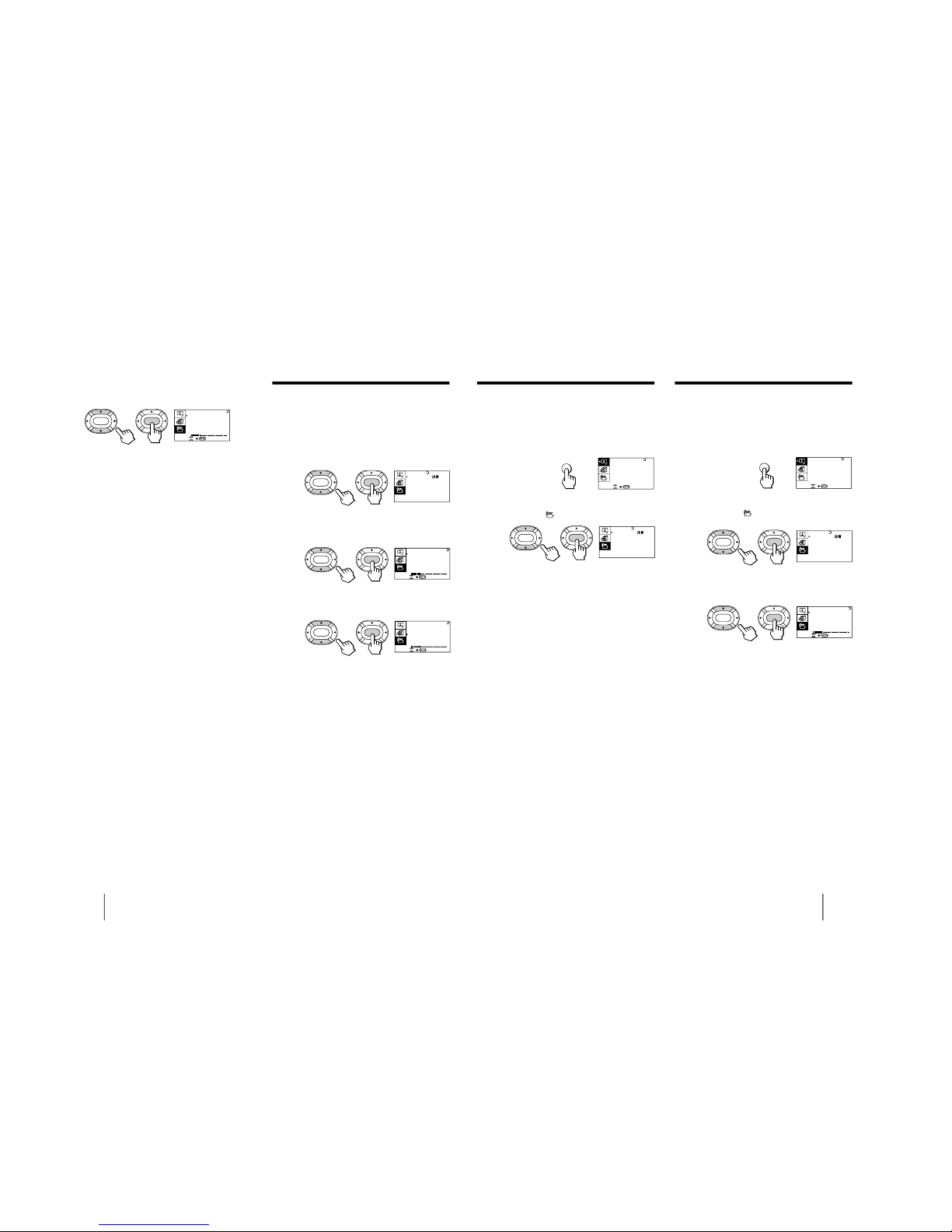
Adjusting the convergence
automatically
Press
on the TV.
The auto convergence function works for about 30
seconds.
Adjusting the convergence manually
When the auto convergence function does not work
correctly with
, adjust convergence by selecting
CONVERGENCE of the FEATURES menu.
1
Press MENU.
2
Press V or v to move the cursor (z) to the
FEATURES menu (
), and press ENTER.
3
Press V or v to move the cursor (z) to
CONVERGENCE and press ENTER.
The CONVERGENCE adjustment screen appears.
4
Press V or v to move the cursor (z) to the
symbol showing the line you want to
adjust, and press ENTER.
: Red vertical line (left/right adjustment)
: Red horizontal line (up/down adjustment)
: Blue vertical line (left/right adjustment)
: Blue horizontal line (up/down adjustment)
R
ENTER
GAME MODE
HYPER SURROUND:
OFF
MONITOR
AV OUT:
FEA TURES
ENTER
ENTER
CONVERGENCE
5
Press V or v to move the line until it
converges with the center green line, and
press ENTER.
To move up/right, press V.
To move down/left, press v.
6
Repeat steps 4 and 5 to adjust the other
lines until all three lines converge and are
seen as a white cross.
7
Press MENU to return to the normal screen.
Adjusting the
convergence
(CONVERGENCE)
R=Red
G=Green
B=Blue
R
G
B
R
G
B
R
G+B
(Light blue)
R
G+B
(Light blue)
/
17
-EN
Operations
PROGR
Watching the TV
1
Press U to turn on the TV.
When the TV is turned on in the standby mode, the
u/Â indicator on the TV lights up. To turn on the
TV completely, press u on the remote commander.
2
Select the TV program you want to watch.
To select a program position directly
Press the number button.
To select a two-digit program position, press “÷”
before the number buttons.
For example: to select program position 25, press
“÷,” then “2” and “5.”
2
-/--
5
Operations
1
2
3
4
5
6
7
8
0
-/--
9
PROGR
To scan through program positions
Press PROGR +/– on the remote commander or the
TV until the program position you want appears.
3
Press Á +/– on the remote commander or
the TV to adjust the volume.
Turning off the TV
To turn off the TV temporarily
Press u on the remote commander. The u/Â
indicator lights up.
To turn off the TV completely
Press U on the TV.
– 10 –
KP-XA43M31/XA43M61/XA43M91
RM-967
Operations
18
-EN
VIDEO 1
VIDEO 2
VIDEO 3
1
DVD
Displaying the on-screen information
Press
.
Note
• The on-screen display shows the program position or the video
mode, the picture and sound information. The on-screen
display for the picture and sound information disappears after
being displayed for approximately three seconds.
Setting the Sleep Timer
You can set the TV to turn off automatically after the
period of time you want.
Press
.
To cancel the Sleep Timer, press
repeatedly until
“SLEEP TIMER: OFF” appears, or turn the TV off.
Watching the video input
Press …
on the remote commander or … on
the TV.
To watch TV
Press ; on the remote commander or … on the TV.
Switching back quickly to the previous
channel
Press JUMP.
Muting the sound
Press ¤.
MUTING
POWER BASSO: ON
DYNAMIC
8
After 30 minutes
After 60 minutes
No Sleep Timer
After 90 minutes
SLEEP TIMER:30M
SLEEP TIMER:60M
SLEEP TIMER:OFF
SLEEP TIMER:90M
19
-EN
Operations
Press V/b
Increase picture
contrast.
Increase color
intensity.
Brighten the picture.
Make picture tones
become greenish.
Sharpen the picture.
Select HIGH to
increase emphasis on
picture edges.
PICTURE
50
90
0
50
VI DEO ADJ UST
COLOR
BRIGHT
HUE
SHARP
VM: HIGH
50
0
ENTER
ENTER
Adjusting the
picture and sound
ENTER
ENTER
MENU
Adjusting the picture settings
(VIDEO ADJUST)
You can adjust the picture settings to suit your taste
with the VIDEO ADJUST option. The adjusted settings
are stored in the PERSONAL option.
1
Press MENU.
2
Make sure the cursor (”) appears in the A/V
CONTROL menu (
), and press ENTER.
3
Press V or v to move the cursor (”) to VIDEO
ADJUST, and press ENTER.
4
Press V or v to move the cursor (”) to the
item you want to adjust, and press ENTER.
5
Press V/b/v/B to adjust the selected item,
and press ENTER.
For details on each item, see “Description of adjustable
items” below.
6
To adjust other items, repeat steps 4 and 5.
7
Press MENU to return to the normal screen.
Description of adjustable items
Item Press v/B
PICTURE Decrease picture
contrast.
COLOR Decrease color
intensity.
BRIGHT Darken the picture.
HUE Make picture tones
become reddish.
SHARP Soften the picture.
VM* Select LOW to
decrease emphasis
on picture edges.
*: Each time you press V/b/v/B, the picture changes as follows:
Note
• You can adjust HUE for the NTSC color system only. (Note
that you can't adjust the NTSC color system of the component
inputs.)
n
HIGH
n
LOW
MENU
ENTER
A / V CONTROL
DYNAM IC
SOFT
STANDARD
PERSONAL
VI DEO ADJ UST
AUDI O AD JUST
MENU
A / V CONTROL
DYNAM IC
SOFT
STANDARD
PERSONAL
V ID EO ADJ UST
AUDI O AD JUST
MENU
Selecting the picture and sound modes
1
Press MENU.
2
Make sure the cursor (”) appears in the A/V
CONTROL menu (
), and press ENTER.
3
Press V or v to move the cursor (”) to
DYNAMIC, STANDARD, SOFT, or PERSONAL,
and press ENTER.
Select To
DYNAMIC Receive high contrast picture with
powerful sound.
STANDARD Receive normal contrast picture with
medium listening sound.
SOFT Receive mild picture with soft sound.
PERSONAL Receive the last picture and sound
settings that are adjusted using VIDEO
ADJUST and AUDIO ADJUST.
4
Press MENU to return to the normal screen.
– 11 –
KP-XA43M31/XA43M61/XA43M91
RM-967
Operations
20
-EN
If the picture is slightly snowy
You may try to improve the picture by changing the
VM setting as described below:
1 Display the VIDEO ADJUST menu.
2 Press V or v to move the cursor (”) to VM, and
press ENTER.
3 Press V/b/v/B to select LOW, and press ENTER.
If the picture color is abnormal when receiving
programs through the ˘ (antenna) terminal
Change the color system or the TV system from the
PRESET menu as described below until the color
becomes normal.
1 Display the PRESET menu.
2 Press V or v to move the cursor (”) to
COL SYS or TV SYS, and press ENTER.
3 Press V/b/v/B to change the color system or the
TV system until the color becomes normal, and
press ENTER.
Note
• Normally set the color system (COL SYS) to AUTO.
Adjusting the sound settings
(AUDIO ADJUST)
You can adjust the sound settings to suit your taste
with the AUDIO ADJUST option. The adjusted settings
are stored in the PERSONAL option.
1
Press MENU.
2
Make sure the cursor (”) appears in the A/V
CONTROL menu (
), and press ENTER.
3
Press V or v to move the cursor (”) to
AUDIO ADJUST, and press ENTER.
4
Press V or v to move the cursor (”) to the
item you want to adjust, and press ENTER.
BASS
80
00
80
TREBLE
BALANCE
AUDI O AD JUST
ENTER
ENTER
SPEAKER:
MAIN
Press V/b
Increase the bass
sound.
Increase the treble
sound.
Increase the right
speaker's volume.
5
Press V/b/v/B to adjust the selected item,
and press ENTER.
For details on each item, see “Description of adjustable
items” below.
6
To adjust other items, repeat steps 4 and 5.
7
Press MENU to return to the normal screen.
Description of adjustable items
Item Press v/B
BASS Decrease the bass
sound.
TREBLE Decrease the treble
sound.
BALANCE Increase the left
speaker's volume
If the sound is distorted or noisy when
receiving programs through the
(antenna)
terminal
Change the TV system from the PRESET menu as
described below until the sound becomes normal.
1 Display the PRESET menu.
2 Press V or v to move the cursor (”) to TV SYS, and
press ENTER.
3 Press V/b/v/B to change the TV system until the
sound becomes normal, and press ENTER.
A / V CONTROL
DYNAM IC
SOFT
STANDARD
PERSONAL
VI DEO ADJ UST
AUDIO ADJUST
MENU
21
-EN
Operations
POWER
BASSO
POWER BASSO: ON
The POWER BASSO sound mode enables you to enjoy
a high quality sound with the best combination of all
types of sound. It reproduces dynamic and clear
sounds and emphasizes low and high audio effects as
well.
Press POWER BASSO.
The sound mode of the TV program or the video input
changes to the POWER BASSO sound.
To cancel the POWER BASSO mode
Press POWER BASSO again.
Note
• You can select any of the surround sound modes (HYPER
SURROUND) to cancel the POWER BASSO sound.
BASS
80
00
80
TREBLE
BALANCE
AUDI O AD JUST
ENTER
ENTER
SPEAKER:
MAIN
BASS
80
00
80
TREBLE
BALANCE
AUDI O AD JUST
ENTER
ENTER
SPEAKER:
MAIN
Listening with
dynamic sound
(POWER BASSO)
A / V CONTROL
DYNAM IC
SOFT
STANDARD
PERSONAL
VI DEO ADJ UST
AUDI O AD JUST
MENU
Setting the speaker
If you connect a Dolby Pro Logic-compatible amplifier
to the center speaker terminals, you can use the
projection TV speakers as center speakers.
1
Press MENU.
2
Make sure the cursor (z) appears in the A/V
CONTROL menu (
), and press ENTER.
3
Press V or v to move the cursor (z) to
AUDIO ADJUST, and press ENTER.
4
Press V or v to move the cursor (z) to
SPEAKER, and press ENTER.
5
Press V/b/v/B to set the speaker, and press
ENTER.
To use the projection TV speakers as center
speakers, select CENTER IN.
To listen to the sound from a projection TV, select
MAIN.
6
Press MENU to return to the normal screen.
– 12 –
KP-XA43M31/XA43M61/XA43M91
RM-967
Operations
22
-EN
MENU
ENTER
GAME MODE
HYPER SURROUND:
OFF
MON I T OR
AV OUT:
FEA TURES
ENTER
ENTER
CONVERGENCE
The HYPER SURROUND feature enables you to enjoy
a surround sound effect that is like being in a concert
hall or movie theater when receiving stereo signals.
1
Press MENU.
2
Press V or v to move the cursor (z) to the
FEATURES menu (
) , and press ENTER.
3
Press V or v to move the cursor (z) to
HYPER SURROUND, and press ENTER.
4
Press V/b/v/B to select MOVIE, MUSIC,
NEWS〈BBE〉, HALL〈SRS〉 or SPACE, and press
ENTER.
MOVIE n
MUSIC nNEWS
〈
BBE
〉
OFF N SPACE N HALL
〈
SRS
〉
N
For details on each item, see “Description of adjustable
items” on the right column.
5
Press MENU to return to the normal screen.
Description of adjustable items
Select To
MOVIE Listen to a sound that emphasizes the bass
audio effect of movie theater.
MUSIC Listen to a dynamic and clear sound that
emphasizes the low and high audio
sounds.
NEWS〈BBE〉 Listen to a sound that emphasizes voice.
HALL〈SRS〉 Listen to a sound that spreads out over a
large area, giving the feeling of being at a
concert hall.
SPACE Listen to a monaural sound that gives a
stereo-like effect.
OFF Turn off the surround sound.
Notes
• The BBE is manufactured by Sony Corporation under license
from BBE Sound, Inc. It is covered by U.S. Patent No. 4,638,258
and No. 4,482,866. The word “BBE” and the BBE symbol are
the trademarks of BBE Sound, Inc.
• The (r)
®
SRS (SOUND RETRIEVAL SYSTEM) is manufactured
by Sony Corporation under license from SRS Labs, Inc. It is
covered by U.S. Patent No. 4,748,669.
The word “SRS” and the SRS symbol (r) are registered
trademarks of SRS Labs, Inc.
Listening to the
surround sound
(HYPER SURROUND)
A / V CONTROL
DYNAM IC
SOFT
STANDARD
PERSONAL
VI DEO ADJ UST
AUDIO ADJUST
MENU
23
-EN
Operations
On-screen display
(Selected sound)
You can enjoy stereo sound or bilingual programs of
NICAM and A2 (German) stereo systems.
Press A/B
repeatedly until you receive the
sound you want.
The on-screen display changes corresponding to the
selected sound and the u/Â indicator also lights up.
When receiving a NICAM program
Broadcasting
NICAM stereo n
NICAM
n
MONO
(Stereo sound) (Regular sound)
NICAM bilingual n
NICAM
n
NICAM
n
MONO
MAIN SUB (Regular sound)
(Main sound) (Sub sound)
NICAM monaural n
NICAM
n
MONO
MAIN (Regular sound)
(Main sound)
When receiving an A2 (German) program
Broadcasting
A2 (German)
stereo
A2 (German)
bilingual
Receiving area for NICAM and A2 (German)
programs
System Receiving area
NICAM Hong Kong, Singapore, New Zealand,
Malaysia, Thailand, etc.
A2 (German) Australia, Malaysia, Thailand, etc.
Notes
• If the signal is very weak, the sound becomes monaural.
• If the stereo sound is noisy when receiving a NICAM program,
select “MONO.” The sound becomes monaural, but the noise is
reduced.
If the sound is distorted or noisy when
receiving a monaural program through the ˘
(antenna) terminal
Press A/B
repeatedly until “MONO” appears on the
screen while the u/Â indicator is off.
To cancel the monaural sound setting, press A/B
again until “AUTO” appears on the screen.
Notes
• The “MONO” or “AUTO” setting memorized for each
program position.
• You cannot receive stereo broadcast signal when the TV is in
the “MONO” setting.
Selecting a stereo or
bilingual program
On-screen display
(Selected sound)
A/B
n
MAIN
n
SUB
(Main sound) (Sub sound)
n
MONO
n
STEREO
(Regular sound) (Stereo sound)
n
MONO
n
AUTO
– 13 –
KP-XA43M31/XA43M61/XA43M91
RM-967
Operations
24
-EN
TV stations broadcast an information service called
Teletext via a TV channel.
Teletext service allows you to receive various
information such as weather forecasts or news at any
time.
Displaying Teletext
1
Select a TV channel that carries the Teletext
broadcast you want to watch.
2
Press
to display the Teletext.
A Teletext page (normally the index page) is
displayed. If there is no Teletext broadcast, “100” is
displayed at the top left corner of the screen.
To turn off Teletext
Press ;.
Superimposing a Teletext page on the
TV picture
Press
.
Each time you press
, the screen changes as follows:
n Teletext n Teletext and TV n TV
Viewing Teletext
Checking the contents of a Teletext
service (INDEX)
Press
to display an overview of the Teletext
contents and page numbers.
Using FASTEXT
This feature allows you to quickly access a Teletext
page that uses FASTEXT. When a FASTEXT program is
broadcasted, the colored menus appear at the bottom of
the screen. The colors of the menus correspond to the
red, green, yellow, and blue colored-coded buttons on
the remote commander.
To access a FASTEXT menu
Press the color-coded button on the remote commander
that corresponds to the colored menu which appears at
the bottom of the screen. The menu page appears on
the screen after several seconds.
Selecting a Teletext page
Press the number buttons to enter the threedigit page number of the Teletext page you
want.
If you make a mistake, re-enter the correct page
number.
To access the next or previous page
Press PROGR +/–.
You can also access a Teletext page of any page
numbers that appear in the colored column at the
bottom of the screen using the corresponding colorcoded button on the remote commander.
Holding a Teletext page (HOLD)
A Teletext page may consist of several subpages. You
can stop the page scrolling in order to read the text at
your own pace.
Press
.
The HOLD symbol “H” appears at the top left corner
of the screen.
To resume normal Teletext operation
Press
again or
.
;
Number
PROGR +/–
Green
Red
Yellow
Blue
1
2
3
4
5
6
7
8
0
9
25
-EN
Operations
Revealing concealed information
(REVEAL)
The REVEAL option lets you disclose concealed
information, such as an answer to a quiz that you find
on some of the Teletext pages.
Press
.
To conceal the information
Press
again.
Enlarging the Teletext display
(ENLARGE)
Press
.
Each time you press
, the Teletext display changes as
follows:
n Enlarge upper half n Enlarge lower half
Normal size N
Waiting for a Teletext page while
watching a TV program (TEXT CLEAR)
1
Enter the page number of the Teletext that
you want to refer to, then press
.
2
When the page number is displayed on the
screen, press
to turn on the Teletext.
Operating optional
components
You can use the supplied remote commander to
operate Sony video equipment such as Beta, 8mm,
VHS, MDP, CD, or DVD.
Setting up the remote commander to
work with other connected equipment
While holding down VIDEO u, press the
following number combinations to enter the
equipment's code number (see the chart
below).
For example, to operate a Sony 8 mm VCR:
Number buttons
MENU
V/b/v/B
/ENTER
VIDEO
u
Video equipment operation
buttons
1
2
3
4
5
6
7
8
0
9
0
2
VIDEO
– 14 –
KP-XA43M31/XA43M61/XA43M91
RM-967
Operations
26
-EN
Operating an MDP using the remote
commander
To
turn on/off
play
stop
pause
step through different
tracks of a disc
Operating a CD/MD using the remote
commander
To
turn on/off
play
stop
pause
go to the next/previous
tracks
go forward ())/backward
(0) quickly in a track
Code numbers for Sony video equipment
To control Hold down VIDEO u and press
DVD 00
VTR1 (Beta) 01
VTR2 (8 mm) 02
VTR3 (VHS) 03
MDP 04
CD 06
MD 07
Notes
• If your video equipment is furnished with a COMMAND
MODE selector, set this selector to the same position as the
setting code.
• If the equipment does not have a certain function, the
corresponding button on the remote commander will not
operate.
• When you remove the batteries, the code number may revert to
the factory setting.
Operating a VCR using the remote commander
To
turn on/off
record
play
stop
fast forward ())
rewind the tape (0)
pause
search the picture forward
()) or backward (0)
Operating a DVD player using the remote
commander
To
turn on/off
play
stop
pause
step through different
tracks of an audio disc
display the Title menu
display the menu
select the menu item
Press
VIDEO u
(
p
P
Press again to resume normal
playback.
+ or
+ or while holding
down (.
Press
VIDEO u
(
p
P
Press again to resume normal
playback.
+ to step forward or to
step backward.
TITLE
MENU while holding down r.
V/v/B/b while holding down
r.
Press
VIDEO u
( while pressing r.
(
p
+
P
Press again to resume normal
playback.
+ or during playback.
Release to resume normal
playback.
+
+
+
Press
VIDEO u
(
p
P
Press again to resume normal
playback.
+ to step forward or to
step backward.
+
+
+
27
-EN
Operations
The GAME MODE feature optimizes the video game
screen by giving a soft picture and dynamic sound
effect.
You can display a video game screen using the button
on the remote commander or the menu.
Press GAME.
The picture and sound change to the mode that is
suitable for video games.
To view a video game screen using the menu
1
Press MENU.
2
Press V or v to move the cursor (z) to the
FEATURES menu (
), and press ENTER.
3
Make sure the cursor (z) appears beside
GAME MODE, and press ENTER.
GAME MODE
HYPER S URROUND:
OFF
MONITOR
AV OUT:
FEA TURES
ENTER
ENTER
CONVERGENCE
Viewing a video
game screen
(GAME MODE)
GAME
GAME
To restore the normal picture and sound
modes
Press ;, …
, or PROGR +/–.
Notes
• If you press the GAME button when the TV is in the standby
mode, the TV turns on automatically and the picture and
sound change to the mode that is suitable for video games.
• To display a video game screen, connect the video game
equipment to the … 3 (video input) jacks at the front or the
rear of the TV.
A / V CONTROL
DYNAM IC
SOFT
STANDARD
PERSONAL
VI DEO ADJ UST
AUDI O AD JUST
MENU
– 15 –
KP-XA43M31/XA43M61/XA43M91
RM-967
Operations
28
-EN
GAME MODE
HYPER SURROUND:
OFF
MON I T OR
AV OUT:
FEA TURES
ENTER
ENTER
CONVERGENCE
Customizing the TV
Using the AV OUT (advanced rec-out)
terminal
You can select the output signal from the Ú (monitor/
TV output) jacks at the rear of the TV. However, the
signals of the PROGRAM INDEX, STROBE, PIP modes,
the signals from the
(component video input)
jacks, and the Teletext broadcast cannot be output even
though MONITOR is selected.
1
Press MENU.
2
Press V or v to move the cursor (z) to the
FEATURES menu (
), and press ENTER.
3
Press V or v to move the cursor (z) to AV
OUT, and press ENTER.
4
Press V/b/v/B to select the output signal,
and press ENTER.
Select To
TV Output the signal of the TV broadcast.
MONITOR Output the signal of the picture you are
watching as a main picture.
Notes
• Do not change the channel while recording with a VCR
through the Ú (monitor/TV output) jacks. If you change the
channel, it also changes the channel you are recording.
• When the signals from the
(component video input) jacks
are displayed on the main screen, the signals can't be output
even though MONITOR is selected.
A / V CONTROL
DYNAM IC
SOFT
STANDARD
PERSONAL
VI DEO ADJ UST
AUDIO ADJUST
MENU
29
-EN
Additional Information
If you have any problems, read this manual again and
check the countermeasure for each of the symptoms
listed below.
If the problem persists, contact your nearest Sony
dealer or authorized service center.
Snowy picture
Noisy sound
/Check the antenna.
/Check the antenna connection on the TV
and on the wall.
/Check the TV system (TV SYS) setting.
/Check the ATT (attenuator) setting.
Dotted lines or stripes
/This may be caused by local interference
(e.g. cars, neon signs, hair dryers, etc.).
Adjust the antenna for minimum
interference.
Double images or “ghosts”
/This may be caused by reflections from
nearby mountains or buildings. A highly
directional antenna may improve the
picture.
Troubleshooting
Good picture
Noisy sound
/Check the TV system (TV SYS) setting.
No picture
No sound
/Press u.
/Press U to turn off the TV for about five
seconds and then turn it on again.
/Check the power cord connection.
/Check the antenna connection.
/Check the VCR connections.
Good picture
No sound
/Press Á +.
/If “CENTER IN” is displayed on the
screen, select “SPEAKER: MAIN” of the
AUDIO ADJUST menu.
/Press ¤.
/Press A/B
.
No color
/Adjust the COLOR level in the VIDEO
ADJUST menu of the PERSONAL option.
/Check the color system (COL SYS) setting.
TV cannot receive stereo broadcast signal
/Press A/B
until “AUTO” appears on
the screen.
TV cabinet creaks
/Even if the picture or the sound is normal,
changes in the room temperature
sometimes make the TV cabinet expand or
contract, making a noise. This does not
indicate a malfunction.
Additional Information
Additional Information

– 16 –
KP-XA43M31/XA43M61/XA43M91
RM-967
Additional Information
30
-EN
Projection system
3 picture tubes, 3 lenses, horizontal in-
line system
Picture tube 7 inch high-brightness monochrome
tubes (6.3 raster size), with optical
coupling and liquidcooling system
Projection lenses High performance, large-diameter
hybrid lens F1.0
Screen size 43 inches
Television system
B/G, I, D/K, M
Color system PAL, PAL 60, SECAM, NTSC
4.43
,
NTSC
3.58
Specifications
Channel coverage
B/G
VHF: E2 to E12
UHF: E21 to E69
CATV: S01 to S03, S1 to S41
I
UHF: B21 to B68
CATV: S01 to S03, S1 to S41
D/K
VHF: C1 to C12, R1 to R12
UHF: C13 to C57, R21 to R60
CATV: Z1 to Z39, S01 to S03, S1 to S41
M
VHF: A2 to A13
UHF: A14 to A79
CATV: A-8 to A-2, A to W+4,
W+6 to W+84
Stereo system NICAM stereo B/G, I, D/K
A2 stereo (German) B/G
Antenna 75 ohm external antenna terminal
Audio output (Speaker)
15 W × 2
Number of terminals
Video Input: 4, Output: 1
phono jacks, 1 Vp-p, 75 ohms
Audio Input: 5, Output: 1, VARIABLE output:
1, phono jacks, 500 mVrms
S video Input: 2,
Y: 1 Vp-p, 75 ohms, unbalanced, sync
negative,
C: 0.286 Vp-p, 75 ohms
Component video
Input: 1, phono jacks
Y: 1.0 Vp-p, 75 ohms, sync negative
C
B
/B-Y: 0.7 Vp-p, 75 ohms
C
R
/R-Y: 0.7 Vp-p, 75 ohms
Audio: 500 mVrms
Headphone Output: 1, minijack
Power requirement
110 – 240 V AC, 50/60 Hz
Power consumption
160 W
Dimensions (w/h/d)
966 × 1074 × 505 mm
Mass Approx. 60 kg
Supplied accessories
Remote commander RM-967 (1)
Size R6 (AA) battery (2)
Optional accessory
TV stand SU-XA43
Design and specifications are subject to change without
notice.
Cleaning the screen
• To clean the screen with a cloth, please use a soft cloth lightly
moistened with a mild detergent solution or water.
Do not use any type of abrasive pad, alkaline cleaner, scouring
powder or solvent, such as alcohol or benzine, or anti static
spray.
As a safety precaution, unplug the TV before cleaning it.
• Do not rub, touch, or tap the surface of the screen with sharp
or abrasive items, like a ball point pen or a screw driver.
Otherwise, this type of contact may result in a scratched
screen.
– 17 –
KP-XA43M31/XA43M61/XA43M91
RM-967
SECTION 2
DISASSEMBLY
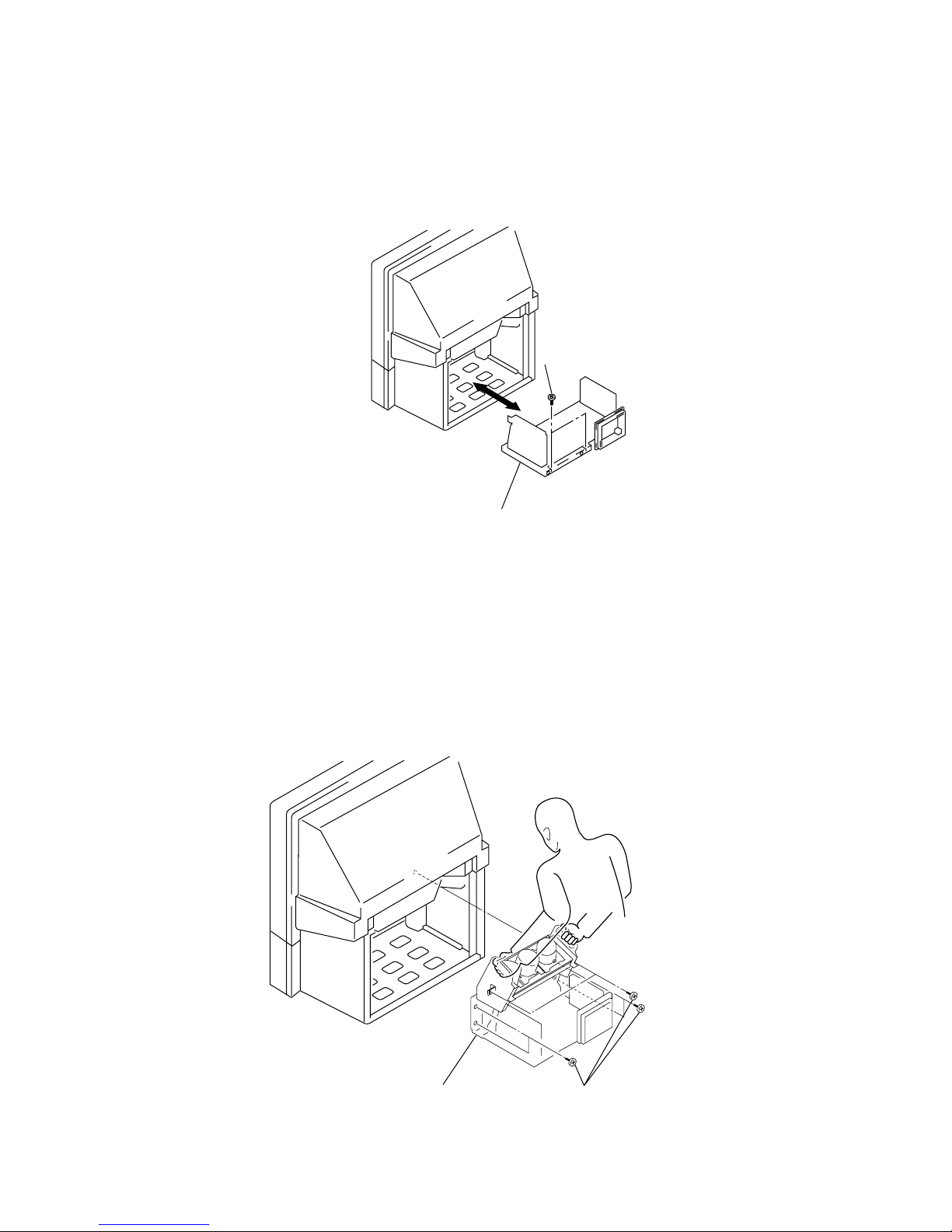
2-1. REAR BOARD REMOVAL
2-3. SERVICE POSITION
2 Rear board
3 Purse lock
1 Thirteen screws
(Hexagon head)
2-2. MAIN BRACKET SECTION REMOVAL
2 Two screws
(BVTP 4X16)
1 Optical shield
3 Main bracket section
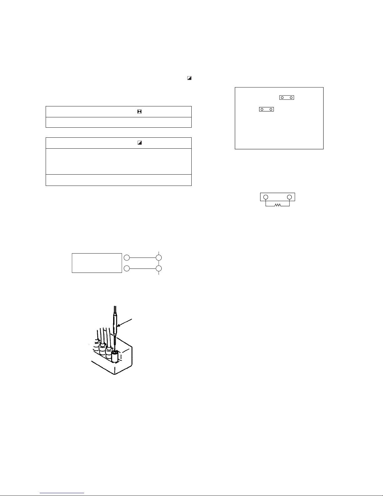
2-4. H1, H2 BOARDS AND RESISTOR
(FOCUS PACK) REMOVAL
Main bracket section
2Grille cover
8Screw (BVTP 4X16)
4Three screws
(BVTP 3X12)
9Resistor (Focus Pack)
3 Speaker grille
7H1 board
6H2 board
5Bracket (H)
1 Four screws
(Hexagon head)
1 Four screws
(BVTP 4X16)
– 18 –
KP-XA43M31/XA43M61/XA43M91
RM-967
2-5. BEZNET SECTION REMOVAL
2 Seven screws
(Hexagon head)
1 Four screws
(Hexagon head)
3 Four screws
(BVTP 4X16)
5 Four screws
(BVTP 4X12)
4 Beznet ass’y
8 Screen holder (H)
!∞ Mirror cover
9 Screen holder (V)
0 Screen holder (H)
!¡ Screen holder (V)
!™ Diffusion plate (F)
!£ Diffusion plate (L)
!¢ Contrast screen
6 Four screws
(BVTP 4X12)
7 Eight screws
(BVTP 4X12)
2-6. G BOARD REMOVAL 2-7. P1 BOARD AND V2 BOARD REMOVAL
1 Three holder PWB
2 G Board
4 V2 board
1 Two claws
3 Two claws
2 P1 board
– 19 –
KP-XA43M31/XA43M61/XA43M91
RM-967
2-8. UG BOARD, AG BOARD AND S BOARD REMOVAL
!¡ S board
0 AG board
4 Screw
(BVTP 4X16)
2 Six screws
(BVTP 3X12)
3 Two screws
(BVTP 4X16)
1 SW screws
(M3X10)
8 Two claws
9 UG board
6 Claw
5 Terminal board
(GA)
7 Bracket (A)
2-9. CHASSIS BLOCK REMOVAL
(1) H1, H2 BOARDS AND RESISTOR REMOVAL
6 Three
connectors
8 Four connectors
1 Four screws
(Hexagon head)
2 Grille cover
0 Screw (BVTP 4X16)
4 Three screws
(BVTP 3X12)
!¡ Resistor (Focus Pack)
3 Speaker grille
9 H1 board
1 Four screws
(BVTP 4X16)
7 H2 board
5 Bracket (H)
– 20 –
KP-XA43M31/XA43M61/XA43M91
RM-967
(2) MAIN BRACKET REMOVAL
* Pay particular attention to the wires of each PCB when puling out the main bracket.
(3) CHASSIS BLOCK REMOVAL
* Pull out the chassis block by gripping the handles as shown in the diagram.
At this time, pay particular attention to the components removed in (1).
1 Two screws
(Hexagon head)
2 Main bracket section
2 Pull the chassis
block.
1 Six screws
(Hexagon head)
– 21 –
KP-XA43M31/XA43M61/XA43M91
RM-967
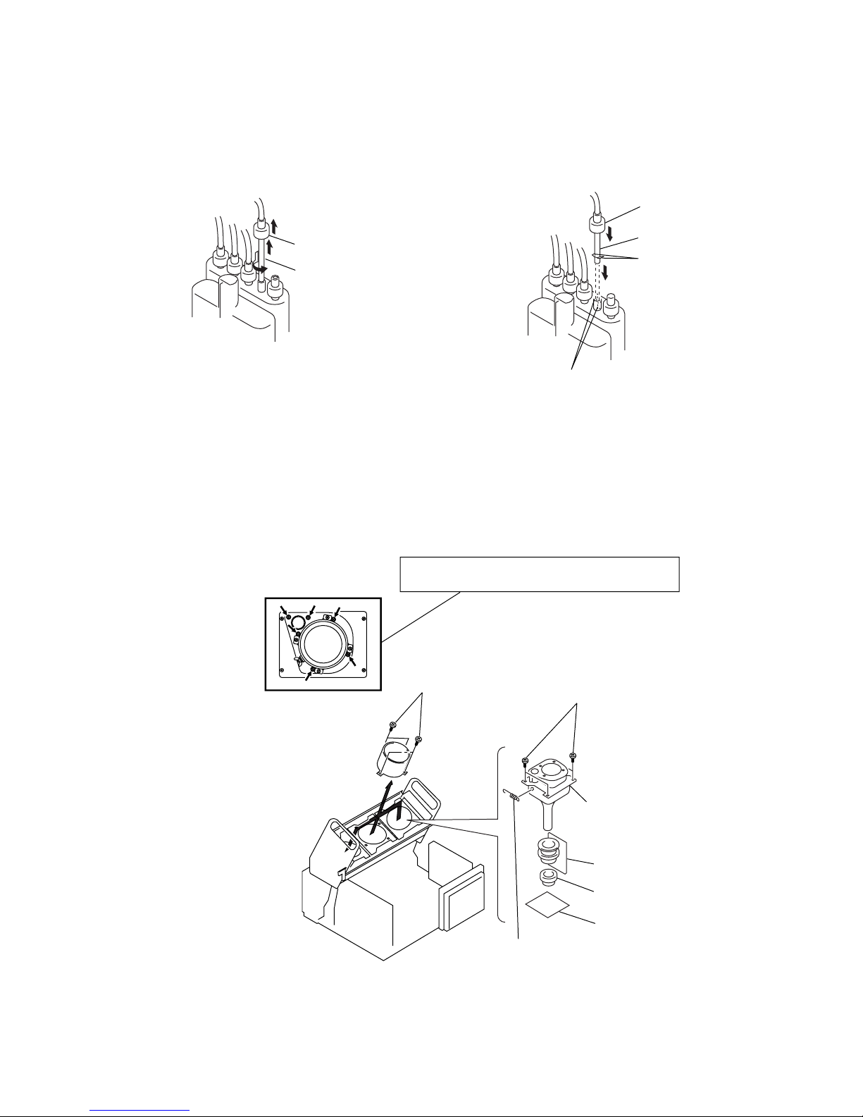
2-10. HIGH-VOLTAGE CABLE INSTALLATION AND REMOVAL
2-11. MECHASEL ASSY REMOVAL
1 Rubber cap
2 HV cable
turn 90°
(1) Remover
2 Rubber cap
1 HV cable
Hook
Gutter
(2) Installation
1 Four screws
(BVTP 4X16)
5 Four screws
(BVTP 4X16)
Removing the arrow-marked screw is strictly inhibited.
If removed, it may cause liquid spill.
2 CR board
3 Neck assy
4 Deflection yoke
6 Mechaseal assy (R)
7 Extension spring
– 22 –
KP-XA43M31/XA43M61/XA43M91
RM-967
SECTION 3
SET-UP ADJUSTMENTS
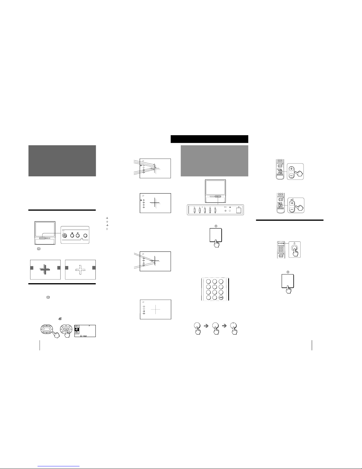
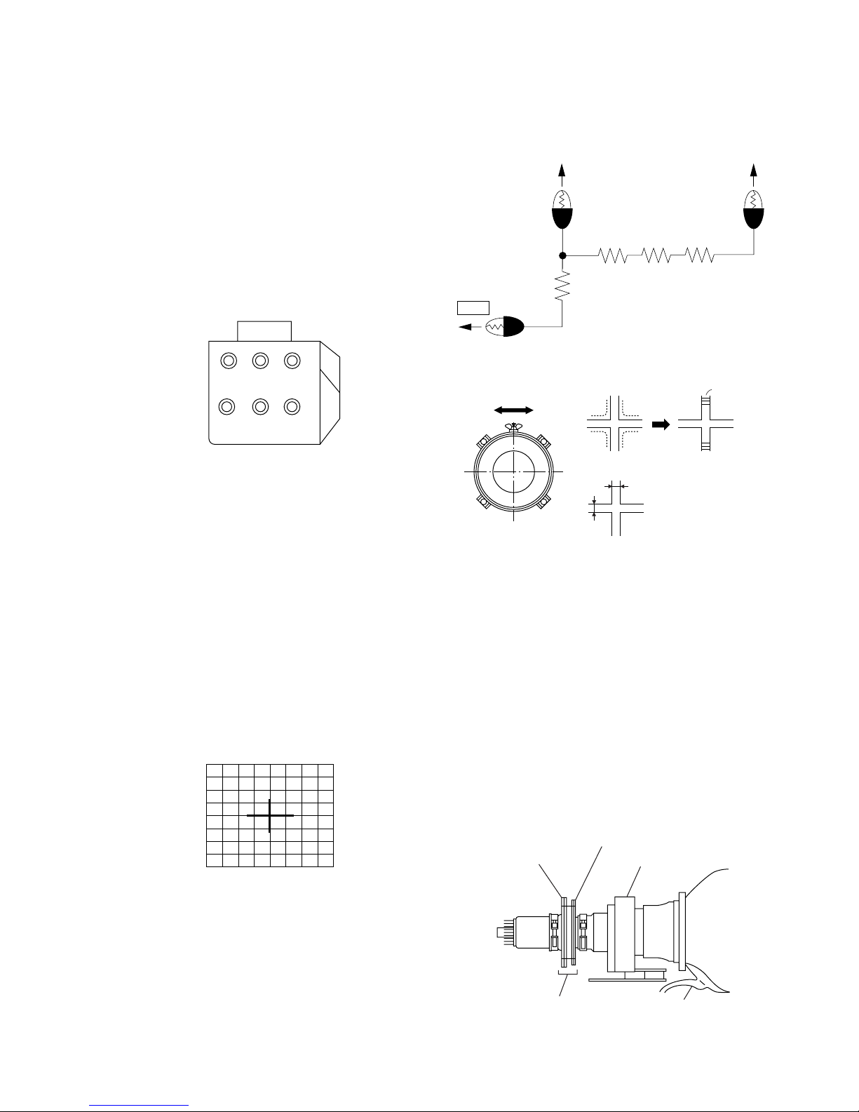
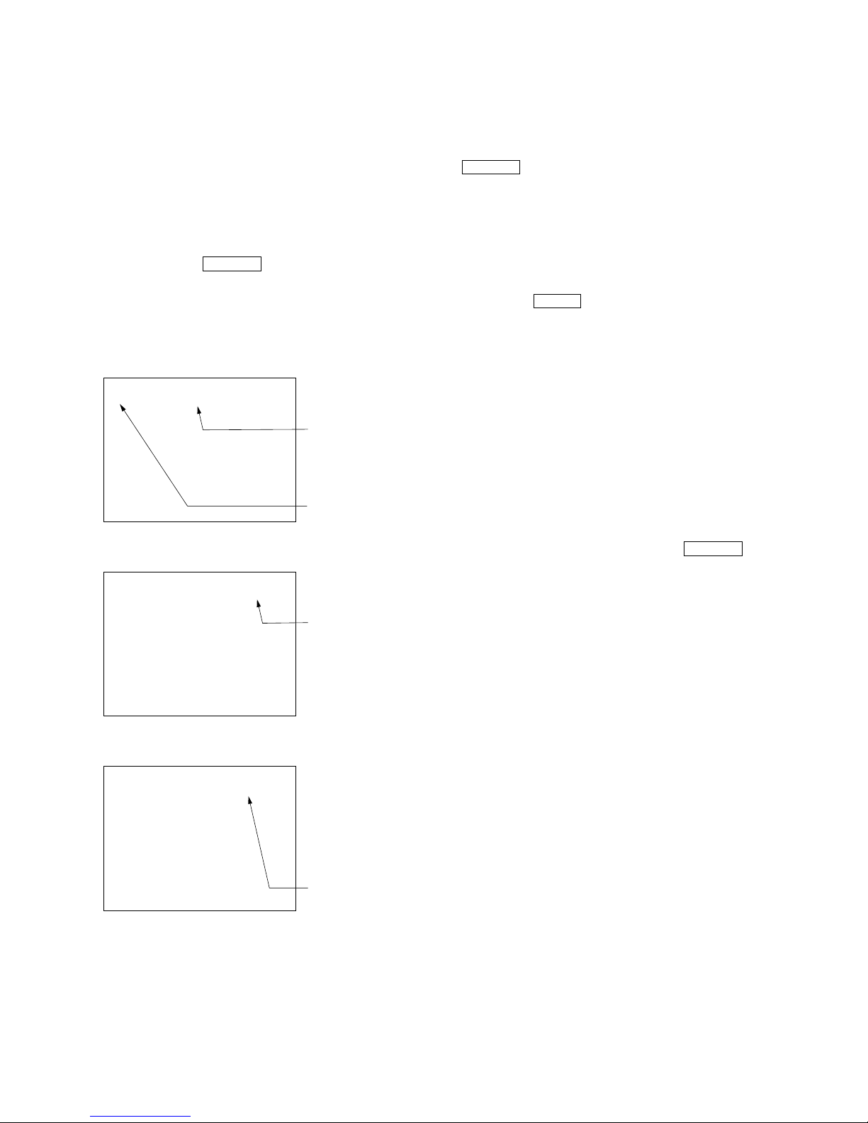
3-1. SCREEN VOLTAGE ADJUSTMENT
(ROUGH ALIGNMENT)
1. Receive the Monoscope signal.
2. Set 50% BRIGHTNESS and minimum PICTURE.
3. Turn the red VR on the FOCUS Pack all the way to the left
and then gradually turn it to the right until the point where
you can see the retrace line.
4. Next gradually turn it to the left to the position where the
retrace line disappears.
Fig. 3-1
Fig. 3-3
Fig. 3-5
Lens
Fig. 3-4
3-2. FOCUS ADJUSTMENT
1. Loose the lens screw.
2. Set in service mode.
3. Place the caps on the red and blue lens so that only the green
color is shown.
4. Press the Commander button and select OSD (CHSW) to
display the test signal (crosshatch) on the screen.
5. Rotate the green lens and align with the optimal focus point
from the test signal.
6. Rotate the green VR on the FOCUS Pack and align to obtain
the optimal focus point.
7. Perform the same alignment for red and blue lenses and elec-
tric focus.
8. Fix lens screw.
Fig. 3-2
Test signal
3-3. SCREEN (G2) ADJUSTMENT
1. Connect JIG (A) to 200 V and GND.
2. Select VIDEO mode without signals.
3. Connect JIG to the TP701(KR), TP731(KG) or TP761(KB)
of CR board, CG board and CB board.
4. Adjust R, G and B screen voltage to until retrace line disap-
pears with screen VR on the focusblock.
3-4. DEFLECTION YOKE TILT ADJUSTMENT
1. Set to receive the Monoscope signal.
2. Set in service mode.
3. Place the caps on the red and blue lens so that only the green
color.
4. Loosen the deflection yoke setscrew and align the tilt of the
Deflection Yoke so that the bars at the center of the monoscope
pattern are horizontal.
5. After aligning the deflection yoke, fasten it securely to the
funnel-shaped portion (neck) of the CRT.
6. The tilt of the deflection yoke for red and Blue is aligned the
same as was done for green.
Fig. 3-6
KR, KG, KB
5.6K/3W X3
<2.2K/3W>
GND
200V
(A)
Neck Assy
2-pole magnet
4-pole magnet
Deflection yoke
Anode cap
RG
SCREEN
B
RG
FOCUS
FOCUS Pack
B
Scanning line visible.
Minimize both A and B.
A
B
– 23 –
KP-XA43M31/XA43M61/XA43M91
RM-967
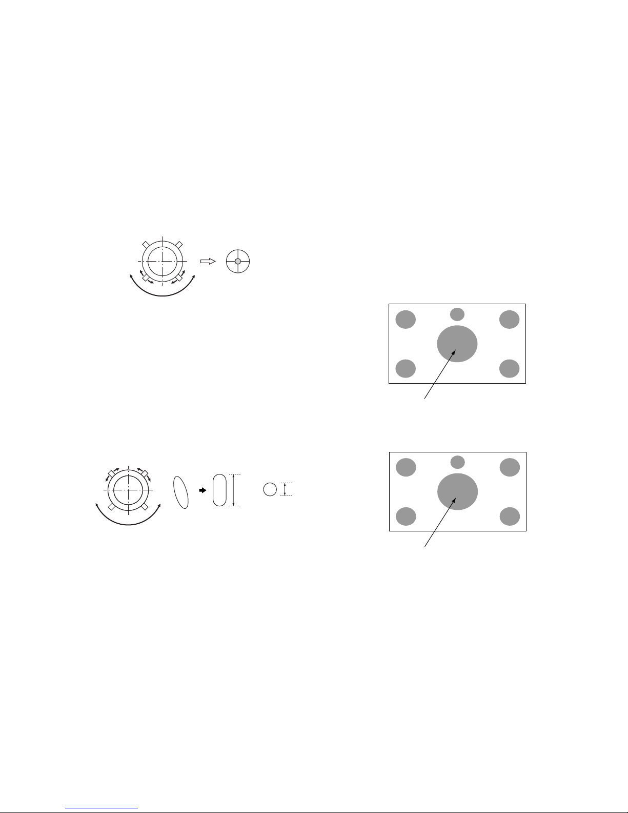
3-5. 2-POLE MAGNET ADJUSTMENT
1. Set in service mode.
2. Set to receive the Dot signal.
3. Place the caps on the red and blue lens so that only the green
color is shown.
4. Turn the green VR on the focus block to the right and set to
overfocus to enlarge the spot.
5. Now align the 2-Pole Magnet so that the enlarged spot is in
the center of the Just Focus spot.
6. Align the green focus VR and set for just (precise) focus.
7. Perform the same alignment for red and blue.
Fig. 3-7
3-6. 4-POLE MAGNET ADJUSTMENT
1. Set in service mode.
2. Set to receive the Dot signal.
3. Place the caps on the red and blue lens so that only the green
color is shown.
4. Turn the green VR on the focus block to the left and set to
underfocus to enlarge the spot.
5. Now align the 4-Pole Magnet so that the enlarged spot becomes a perfect circle.
6. Perform the same alignment for red and blue.
Fig. 3-8
3-7. DEFOCUS ADJUSTMENT (Blue)
1. Receive the Dot signal.
2. Place the caps on the red and green lens so that only the blue
color is shown.
3. Rotate the blue focus volume on the focus pack and adjust to
obtain best electrical focus.
4. Rotate Blue focus volume of focus pack clocwise, so that
diameter of the Dot see Caution.
3-8. GREEN AND RED FOCUS ADJUSTMENT
3-8-1. Green and Red Lens Focus Adjustment
1) Input a monoscope signal.
2) Place a lens cover over Red and Blue lenses and project only
Green.
3) Rotate the Green lens and ajust to obtain the best lens focus.
4) Fix lens screw.
5) Repeat above process for Red.
3-8-2. Green and Red Electrical Focus Adjustment
1) Input a monoscope signal.
2) Project only Green.
3) Rotate the green focus volume on the focus pack and adjust
to obtain an optimal electrical focus in the top right corner,
taking care of center focus is not NG. obtain a compromise
between center and corner focus.
4) Repeat above process for Red.
Fig. 3-11
Fig. 3-12
Adjust Point
Use the center dot
Use the center dot
y
x : y = 1 : 2
x
Blue Defocus just focus
Adjust Point
– 24 –
KP-XA43M31/XA43M61/XA43M91
RM-967
SECTION 4
SAFETY RELATED ADJUSTMENT
When replacing the following components marked with
on the schematic diagram, always check hold-down volt-
age and if necessary re-adjust.
4-1. HV HOLD-DOWN ADJUSTMENT
1. Remove CN810. Connect HV meter to HV Block.
2. Connect External Power Supply to CN810 2 pin
(+135V) and 1 pin (GND).
Part Replaced ( )
E Board C515, C516, C554, D504, D507,
L506, Q502, R1, R514, R516,
R517, T502, T504 (FBT)
G Board IC6008
Part Replaced ( )
R1
3. Turn on the set.
4. Slowly up the supply voltage from 0V to 135V.
5. Receive dot picture and set PICTURE/BRIGHT-
NESS to minimum.
6. Slowly up the voltage until hold-down circuit works
(picture disappear).
7. Read the HV meter of peak HV voltage.
Spec: 34.5±0.75KV
8. If Hold-down voltage is less than 33.75KV then sol-
der R1=820K.
9. If hold-down voltage is over than 35.25KV then
take-off R514 and solder R1=9.1K.
+
–
2
CN810
Power
Supply
1
E BOARD
– CONDUCTOR SIDE –
CN810
CN505
CN505
R1
Fig. 4-1
Fig. 4-2
Fig. 4-3
Fig. 4-4
Remove the cap off
from the unused
terminal and connect a
static voltmeter there.
– 25 –
KP-XA43M31/XA43M61/XA43M91
RM-967
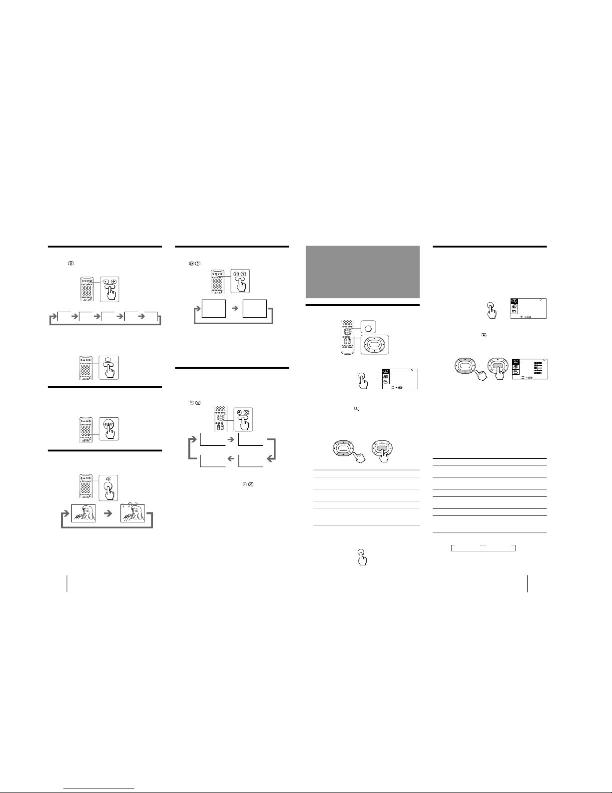
Entering service mode
With the unit on standby
↓
+
↓
5
↓
Á
↓
The operation sequence puts the unit into service mode.
SECTION 5
CIRCUIT ADJUSTMENTS
5-1. ADJUSTMENTS WITH COMMANDER
Service adjustments are made with the RM-871 that comes with
this unit.
1, 4 Select the adjustment item.
↓
3, 6 Raise/lower the data value.
↓
MUTING Writes.
↓
0 Executes the writing.
7, 0 All the data becomes the values in memory.
8, 0 All user control goes to the standard state.
5, 0 Service data initialization (Be sure not to use
usually.)
+ , 0 Write 50Hz adjustment data to 60Hz, or vice
versa. (not to use 2, 0 .)
The screen display is :
RM-967
Depends on the signals
PAL, SECAM : 50
NTSC : 60
00 VSH 1F SERVICE 50
XXX 00 00 00 20V2 1C
DATA
Mode
Adjstment item
Item number
SOFTWARE VERSION
H SYNC COUNTEROEM CODE
PROGR
MENU
A/B
GAME
1
2
3
4
5
6
7
8
0
-/--
9
ENTER
POWER
BASSO
TITLE
VIDEO
– 26 –
KP-XA43M31/XA43M61/XA43M91
RM-967
5-2. ADJUSTMENT METHOD
Item Number 00
This explanation uses V-Position as an example.
1. Select 00 VSH with the 1 and 4 buttons.
2. Raise/lower the data with the 3 and 6 buttons.
3. Select the optimum state. (The standard is IF for PAL
reception.)
4. Write with the MUTING button. (The display changes to
WRITE.)
5. Execute the writing with the - button. (The WRITE
display will be changed back to SERVICE.)
Use the same method for Items Number 00-99. Use 1 and 4
to select the adjustment item, use 3 and 6 to adjust, write with
MUTING , then execute the write with -.
• As for V-FREQ, by searching the bolded screen V range with
adjusting data.
Note : 1. For adjustment Items that have differnt standard data
between 50Hz or 60Hz and normal or wide, be sure to
use the respective input signal while adjusting.
2. In WRITE , the data for all items are written into
memory.
The display change from
SERVICE to WRITE.
1FVSF00
Data adjusted with
3 and 6 buttons.
Item selected with
1 and 4 buttons.
1FVSF
Written with [MUTING]
Write executed with [0]
The WRITE display
then changes back
to SERVICE.
1FVSF00
SERVICE 50
WRITE 50
WRITE 50
00
5-3. ADJUSTMENT AFTER IC1001 and IC1702
REPLACEMENT
1. Enter to Service Mode.
2. Change IC1001 (Except for Registration Adjustment).
Change IC1702 (Only Registration Adjustment).
3. Call each item number, and check if the respective screen
shows the normal picture.
In cases where items are not well adjusted, recitify the items
with fine adjustment.
Write the data per each item number ( MUTING + - )
4. Select item numbers “98” (OP0) and “99” (OP1) and respec-
tively set the bit per model with command buttons 3 and
6.
– 27 –
KP-XA43M31/XA43M61/XA43M91
RM-967
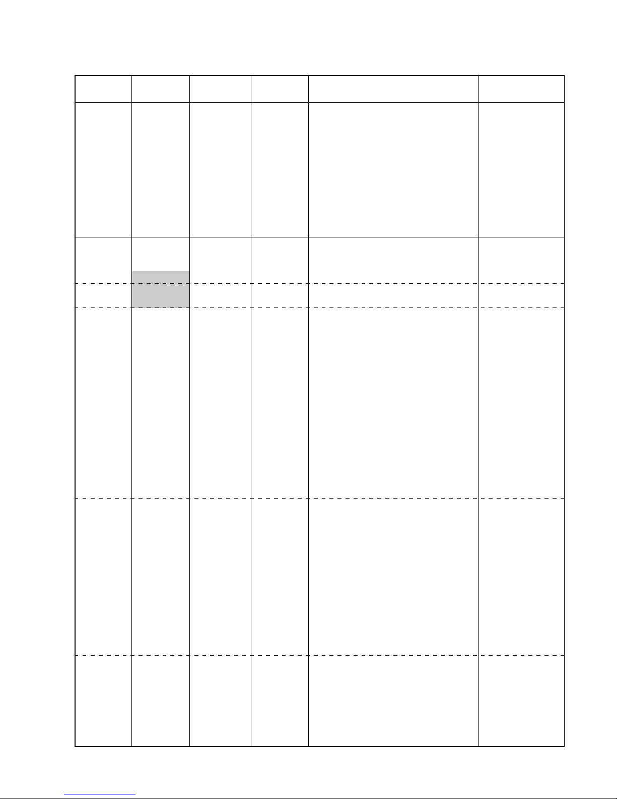
Item Adj Data Std Register
Device
Display Item Range Values Name
00 VSH 00~3F 1B V POSITION CXA2050S
01 VSZ 00~3F 21 V SIZE
02 HSH 00~0F 07 H POSITION
03 HSZ 00~3F 12 H SIZE
04 SCR 00~0F 06 S CORRECTION
05 VLN 00~0F 08 V LINEARITY
06 PAP 00~3F OE PIN COMP
07 PPH 00~0F 05 PIN PHASE
08 UCP 00~0F 05 UP CORNER PIN
09 LCP 00~0F 05 LOW CORNER PIN
0A BOW 00~0F 05 AFC-BOW
0B ANG 00~0F 09 AFC-ANGLE
OSD0 CHSW 0,1 0 Hatch Display
(0: Disp Hatch, 1: No Disp) CXP86213-002S
OSD1 OSDH 1-32 10 OSD H POS
OSD2 OSDV 1-32 10 OSD V POS
OSD3 VMRK 0,1 0 V SIZE Mark
SFT0 SFTE 0,1 1 Shift Enable
SFT1 SFTF 0,1 0 Shift Fast
GH0 GSEL 0,1 0 OSD Select for GH, GV
(0: G + R, 1: Green)
GH1 CENT –127~+127 0 CENTER
GH2 SKEW –127~+127 0 SKEW
GH3 BOW –127~+127 0 BOW
GH4 4bow –127~+127 0 4th BOW
GH5 SIZE –127~+127 0 SIZE
GH6 LIN –127~+127 0 LINEARITY
GH7 MSIZ –127~+127 0 MID SIZE
GH8 MLIN –127~+127 0 MID LINEARITY
GH9 KEY –127~+127 0 KEYSTONE
GH10 SSKW –127~+127 0 SUB SKEW
GH11 MPIN –127~+127 15 MID PINCUSION
GH12 PIN –127~+127 –12 PINCUSION
GH13 SBOW –127~+127 8 SUB BOW
GH14 MBOW –127~+127 0 MID BOW
GH15 4PIN –127~+127 0 4th PINCUSION
GH16 4SBO –127~+127 0 rth SUB BOW
GV0 CENT 0 0 CENTER
GV1 SKEW –127~+127 0 SKEW
GV2 BOW –127~+127 0 BOW
GV3 SIZE –127~+127 0 SIZE
GV4 LIN –127~+127 0 LINEARITY
GV5 MSIZ –127~+127 0 MID SIZE
GV6 MKEY –127~+127 0 MID KEYSTONE
GV7 KEY –127~+127 0 KEYSTONE
GV8 SSKW –127~+127 0 SUB SKEW
GV9 MPIN –127~+127 0 MID PINCUSION
GV10 PIN –127~+127 20 PINCUSION
GV11 SBOW –127~+127 16 SUB BOW
GV12 WAVE –127~+127 0 WAVWE
GV13 4PIN –127~+127 25 4th PINCUSION
RH0 CENT –95~+96 0 CENTER
RH1 SKEW –95~+96 0 SKEW
RH2 BOW –127~+127 0 BOW
RH3 4BOW –127~+127 0 4th BOW
RH4 SIZE –127~+127 25 SIZE
RH5 LIN –127~+127 10 LINEARITY
RH6 MSIZ –127~+127 30 MID SIZE
RH7 MLIN –127~+127 –30 MID LINEARITY
Adjustment Item Table
– 28 –
KP-XA43M31/XA43M61/XA43M91
RM-967
RH8 KEY –127~+127 0 KEYSTONE
RH9 SSKW –127~+127 0 SUB SKEW
RH10 MPIN –127~+127 0 MID PINCUSION
RH11 PIN –127~+127 –10 PINCUSION
RH12 SBOW –127~+127 40 SUB BOW
RH13 MBOW –127~+127 12 MID BOW
RH14 4PIN –127~+127 0 4th PINCUSION
RH15 4SBO –127~+127 0 4th SUB BOW
RV0 CENT –95~+96 –10 CENTER
RV1 SKEW –95~+96 0 SKEW
RV2 BOW –127~+127 4 BOW
RV3 SIZE –127~+127 0 SIZE
RV4 LIN –127~+127 0 LINEARITY
RV5 MSIZ –127~+127 0 MID SIZE
RV6 MKEY –127~+127 10 MID KEYSTONE
RV7
KEY KEYSTONE
–10 –10 –127±127
RV8 SSKW –127~+127 10 SUB SKEW
RV9 MPIN –127~+127 0 MID PINCUSION
RV10
PIN PINCUSION
10 10 –127±127
RV11 SBOW –127~+127 16 SUB BOW
RV12 WAE –127~+127 30 WAVE
RV13 4PIN –127~+127 10 4th PINCUSION
RV14 MWAVE –31~+31 0 MID WAVE
BH0 BSEL 0,1 0 OSD Select for BH, BV
(0: B + G, 1: B + R)
BH1 CENT –95~+96 0 CENTER
BH2 SKEW –95~+96 0 SKEW
BH3 BOW –127~+127 0 BOW
BH4 4BOW –127~+127 0 4th BOW
BH5 SIZE –127~+127 –25 SIZE
BH6 LIN –127~+127 –10 LINEARITY
BH7 MSIZ –127~+127 30 MID SIZE
BH8 MLIN –127~+127 30 MID LINEARITY
BH9 KEY –127~+127 0 KEY KEYSTONE
BH10 SSKW –127~+127 0 SUB SKEW
BH11 MPIN –127~+127 0 MID PINCUSION
BH12 PIN –127~+127 –10 PINCUSION
BH13 SBOW –127~+127 –40 SUB BOW
BH14 MBOW –127~+127 –16 MID BOW
BH15 4PIN –127~+127 0 4PIN 4th PINCUSION
BH16 4SBO –127~+127 0 4th SUB BOW
BV0 CENT –95~+96 –10 CENTER
BV1 SKEW –95~+96 0 SKEW
BV2 BOW –127~+127 0 BOW
BV3 SIZE –127~+127 0 SIZE
BV4 LIN –127~+127 0 LINEARITY
BV5 MSIZ –127~+127 0 MID SIZE
BV6 MKEY –127~+127 –10 MID KEYSTONE
BV7 KEY –127~+127 10 KEYSTONE
BV8 SSKW –127~+127 –10 SUB SKEW
BV9 MPIN –127~+127 0 MID PINCUSION
BV10 PIN –127~+127 10 PINCUSION
BV11 SBOW –127~+127 32 SUB BOW
BV12 WAVE –127~+127 –30 WAVE
BV13 4PIN –127~+127 10 4th PINCUSION
BV14 MWAVE –31~+31 0 MID WAVE
ACV0 ART0 1-8 6 DATA SAMPLE LENGTH
ACV1 AT1M 0-255 1S SAMPLE START TIME (UP)
Item Adj Data Std Register
Device
Display Item Range Values Name
– 29 –
KP-XA43M31/XA43M61/XA43M91
RM-967
ACV2 AT1M 0-255 132 SAMPLE START TIME (LSR)
ACV3 AT1B 0-255 240 SAMPLE START TIME (BOT)
ACV4 AH51 0-255 1S OSD H POS 50 (L & R)
ACV5 AH52 0-255 130 OSD H POS 50 (UP & BOTTOM)
ACV6 AV5T 0-255 1 OSD V POS 50 (UP)
ACV7 AV5M 0-255 60 OSD V POS 50 (L & R)
ACV8 AV5B 0-255 130 OSD V POS 60 (BOTTOM)
ACV9 AH61 0-255 18 OSD H POS 60 (L & R)
ACV10 AH62 0-255 130 OSD H POS 60 (BOTTOM)
ACV11 AV6T 0-255 1 OSD V POS 50 (UP)
ACV12 AV6M 0-255 46 OSD V POS 50 (L & R)
ACV13 AV6B 0-255 100 OSD V POS 50 (BUTTOM)
ACV14 RHCO –127~+127 0 RH CENT ADJ OFFSET
ACV15 BHCO –127~+127 0 BH CENT ADJ OFFSET
ACV16 RCO –127~+127 0 RV CENT ADJ OFFSET
ACV17 BVCO –127~+127 0 BV CENT ADJ OFFSET
ACV18 RHSO –127~+127 0 RH SKEW ADJ OFFSET
ACV19 BHSO –127~+127 0 BH SKEW ADJ OFFSET
ACV20 RVSO –127~+127 0 RV SKEW ADJ OFFSET
ACV21 BVSO –127~+127 0 BV SKEW ADJ OFFSET
ACV22 AERR 0-255 0 AUTO CONV. ERROR CODE
MSC0 ACTL 0-255 0 COUNTER (LOW BYTE)
MSC1 ACTH 0-255 0 COUNTER (HIGH BYTE)
0C VAP 00~3F 2F V ASPECT CXA2050S
0D VSC 00~3F 1F V SCROLL
0E ULN 00~0F 00 UP V LINEARITY
0F LLN 00~0F 00 LOW V LINEARITY
10 EHH 00~03 00 EHT-H
11 EHV 00~03 00 EHT-V
12 HBS 00~01 01 H BLK WID.ON/OFF
13 LBK 00~0F 0F L BLK WIDTH
14 RBK 00~0F 0F R BLK WIDTH
15 JSW 00~01 00 JUMP ON/OFF SW
16 VBW 00~03 02 V BLK WID.CON.
17 AFC 00~03 01 AFC-MODE
03
18 FHH 00~01 00 FH-HI
19 VFQ 00~03 00 V-FREQ
1A VOF 00~01 00 V OFF
1B VMD 00~01 00 CD-MODE2
1C CMD 00~01 00 CD-MODE
1D TTL 00~03 00 INTERLACE
1E ZSW 00~01 00 ZOOM SW
1F POV 00~03 02 PRE-OVER
20 CT1 00~01 01 C-TRAP(NTSC)
21 CT2 00~01 01 C-TRAP(PAL)
22 CFO 00~0F 07 C-TRAP fo ADJ
23 SFO 00~01 00 SHARPNESS fo ADJ
24 TOT 00~01 01 TOT FILTER SW
25 CSW 00~03 00 COLOR SW
26 XTL 00~03 00 XTAL
00
27 CV1 00~01 01 CV/YC SEL(NTSC)
28 CV2 00~01 01 CV/YC SEL(PAL)
29 VM 00~01 01 VM ON/OFF
2A YVM 00~01 00 YS1/VM SW(0:YS1)
2B DPC 00~01 01 D-PIC ON/OFF
Item Adj Data Std Register
Device
Display Item Range Values Name
 Loading...