

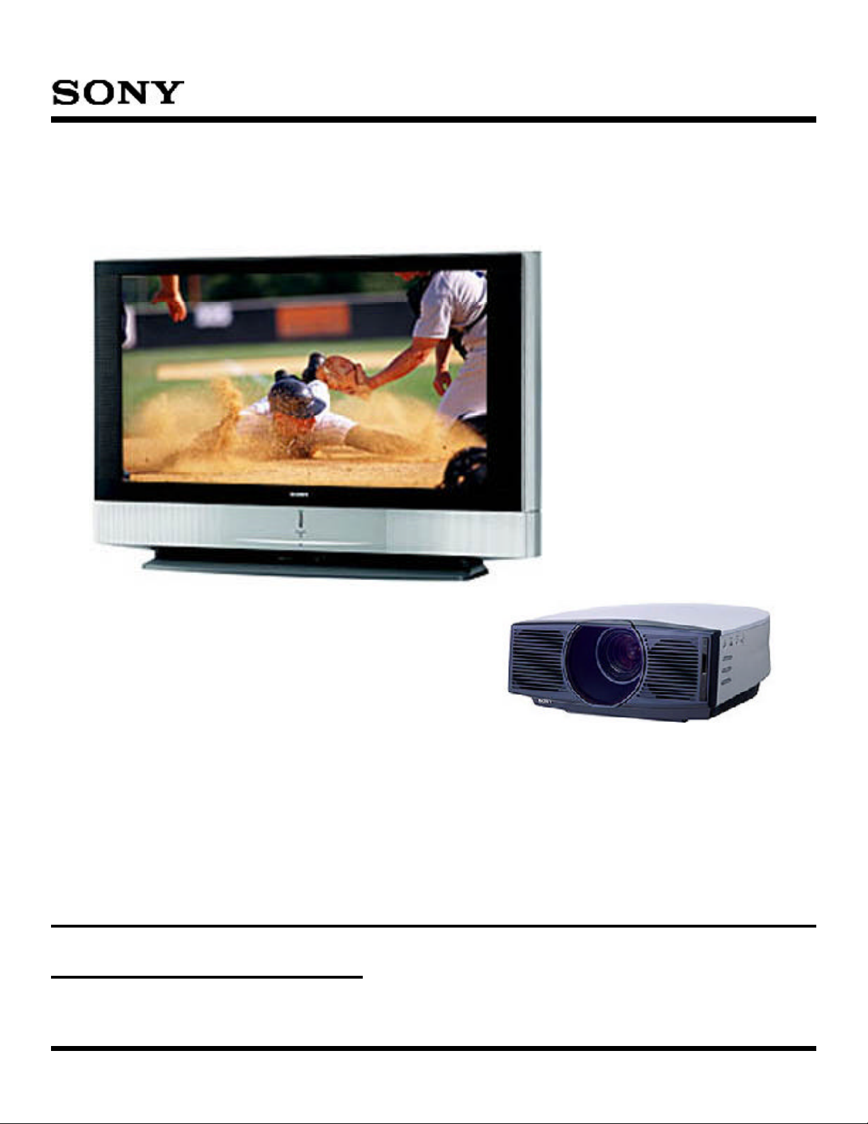
SONY VPL-HS20 Training Manual
Training Manual
KP-60WE610
LA-2 Chassis
Models: KP-42WE610
KP-50WE610
KP-60WE610
KFD-60XBR950
KFD-70XBR950
VPL-HS20
Diagnostics and Troubleshooting
VPL-HS20
Course: TVP-17

Table of Contents
Introduction...........................................1
1. The LA-2 Chassis ............................2
Overview................................................................. 2
Circuit Layout ......................................................... 3
Circuit Board Locations ........................................ 6
2. LA-2 Power Supplies.......................7
Overview................................................................. 7
Troubleshooting..................................................... 10
3. LA-2 Protect & Self-Diagnostics ..12
Overview................................................................ 12
Direct Relay Deactivation Protection ................. 12
Protection and Self-Diagnostics ......................... 14
Entering Diagnostics Mode................................. 16
4. LA-2 Video Processing..................17
Overview................................................................ 17
Video Input & Switching ....................................... 17
Video Processing ................................................. 19
Troubleshooting..................................................... 22
Internal Pattern Generator.................................... 27
6. The VPL-HS20 .................................32
Overview................................................................ 32
Overall Block diagram.......................................... 32
7. Power Supply ..................................35
Overview................................................................ 35
Theory of Operation.............................................. 35
Power Supply Troubleshooting............................ 39
8. Protect Circuits ...............................41
Overview................................................................ 41
9. Video Circuits ..................................45
Video Input Selection ........................................... 45
B Board Video Processing ................................. 47
C Board Video Processing ................................. 48
Troubleshooting..................................................... 49
10. Servicing the VPL-HS20 ..............53
Overview................................................................ 53
Disassembly.......................................................... 54
Servicing the Prism Block.................................... 56
Service Mode........................................................ 60
5. LA-2 Audio Processing..................30
Overview................................................................ 30
Circuit Description................................................ 30
Additional Service Tips ........................................ 61

TVP-17 - Introduction
TVP-17 - Introduction
The last several years have seen dramatic growth in the number of display products utilizing Liquid Crystal
Display devices for both direct and projection-type televisions for motion video viewing. In a market long dominated
by the cathode-ray tube, LCD technology has slowly overcome the inherent flaws of this display device, particularly
geometric distortion. LCD technology has been around for over three decades; however, certain limitations
prevented it from immediately replacing the CRT displays. Although other technologies exist such as Plasma
and DLP, their costs remain relatively high. LCD provides for a middle ground and is currently the best display
format for the price.
One of the limitations slowing LCD technology for use in motion picture display was its extreme lack of contrast
compared to the CRT. Original liquid-crystal designs used a scan pulse to select a particular pixel and a variable
voltage to change the amount of “twist” in the crystals to vary the amount of light passing through, usually from
a backlight source. Capacitors across these terminals would slow the rise time of the control voltage. Cross-talk
among pixels also contributed to unacceptable contrast levels for television viewing since each horizontal line of
pixels is selected, causing the charge among the capacitors to leak across the rows. This is known as “Passive
Matrix”.
By adding thin-film transistors (TFT), greater control can be achieved at each pixel and a dramatic increase in
contrast and resolution is seen. Earlier versions of TFT displays were still quite a ways off from the contrast ratio
achieved by CRTs and struggled to generate contrast ratios exceeding 600:1. Newer design LCD panels have
more than doubled this ratio to 1600:1 and, although still below CRT, DLP and plasma levels, the picture quality
of the newest generation of LCD projection televisions has risen to a level that rivals these other technologies.
This has generated a dramatic rise in sales of LCD-driven televisions.
The purpose of this manual is to introduce Sony’s newest models of front and rear projection display products.
Five new Grand Wega® models have been introduced for the year 2004. The WE series, starting with model
KF42WE610, is also available in a 50" and 60" screen size. They utilize a new chassis design known as the LA2 chassis. A new XBR series (KDF60/70XBR950) is also available with the LA-2A chassis. Differences between
the chassis are minimal and the material in this training manual will provide adequate material to understand
both.
Front projection televisions have also been gaining popularity among consumers for their high brightness, resolution
and viewing angles. They are the display of choice in many high-end entertainment systems. This course will
also cover the model VPL-HS20 LCD projector.
The use of LCD displays along with numerous digital processing circuits has introduced the need for
troubleshooting methods different from those that most technicians are accustomed. Descriptions of the
various circuits along with practical troubleshooting methods will be discussed to assist in a quick and
accurate diagnosis as to what area a failure may be located. The repair policy as of this writing involves
board-level repair but still requires knowledge of the various processing stages to properly isolate which board
should be replaced.
1

1. The LA-2 Chassis
Chapter 1 - The LA-2 Chassis
Overview
The LA-2 chassis represents the third generation of the Grand Wega™ Television series. The first production
models included the KF42/50/60WE610. An XBR® series using the LA-2 chassis appeared shortly thereafter,
designated as the KFD60/70XBR950. Both chassis are similar with the primary difference being the inclusion of
an ATSC decoder on the XBR models to receive both VSB and QAM DTV signals.
Various changes and improvements have been implemented to produce a significant improvement in picture
quality over previous models.
• The Sony Wega Engine™: Incoming analog video signals are converted to digital and remain in this
state all the way to the LCD panels. Eliminating the A/D and D/A conversions performed in prior designs
increases picture quality.
• New Optical Engine Design: The optical block assembly has been reduced in size by approximately
25%. The LCD panels have been reduced from 1.35 inches to 0.87 inches while still increasing the pixel
resolution from 1366 X 768 to 1386 X 788 (WXGA resolution) to provide 3.28 million dots. A new lamp
design utilizing a high pressure, mercury gas lamp with a 1mm arc gap along with a smaller lamp driver
power supply also adds to the size reduction.
• Memory Stick® Video Playback: MPEG1 video and audio recorded to a Memory Stick® can now be
played along with JPEG still pictures.
• Three Speaker Sound System (WE series only) : Separate woofer and L/R amplifiers along with a
three-dimensional sound system to simulate surround sound. The XBR series incorporates a sevenspeaker system.
• Improved Black Level : Contrast ratios closer to those found on CRT devices are now available. Creating
a small drop in lamp-drive voltage accomplishes this when the Cinema-Black ™ feature is selected.
2
1. The LA-2 Chassis
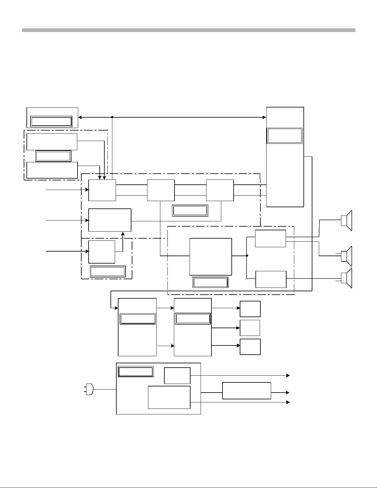
Circuit Layout
Figure 1-1 shows an overall block diagram of the LA-2 chassis. There are 16 circuit boards utilized in the
chassis. Only the large boards containing key components are shown in the illustration. Below is a list of
each circuit board and its particular function(s):
MEMORY STICK
MS2A BOARD
DIC2
MAIN TUNER
A BOARD
SUB TUNER
BOARD
VIDEO
1~4
VIDEO
5-6
VIDEO 7
DVI
AV
SW1
COMPONENT
DVI
I/F
UD BOARD
MAIN V
SUB V
I/F
C2 BOARD C1 BOARD
AV
SW2
MAIN V
SUB V
A BOARD
SURROUND
PROCESSOR
AU BOARD
VIDEO
SW
MAIN V
SUB V
LCDR
LCDG
LCDB
L/R
AMP
WOOFER
AMP
L.R
WOOFER
G1 BOARD
STBY
CONV
MAIN
CONV
LAMP
DRIVER
FIGURE 1-1 - LA-2 CHASSIS OVERALL BLOCK
3
TVP17.1-1 1/30/04

1. The LA-2 Chassis
• A Board: Essentially doubling as a motherboard, the G (power supply), DIC2 (video processing) and C2
(digital processing) are mounted to it with multi-connectors. Key components found on this board are:
The main and sub tuner, analog video signal buffers, audio circuits for the woofer amp, a systems control
IC dedicated to controlling the drive ICs for the fan motors and SIRCS communications. Regulator
circuits are also present for LVDS3.3V, MS3.3V and STBY5V.
• AU Board: Audio processor for simulated surround sound along with the L/R amplifiers.
• C1 Board: This board is located on the optical block assembly. The primary function is to drive the three
LCD panels. Two LVDS receivers (this will be covered later) receive digital video data from the C1 board.
Gamma correction data is stored in an on-board NVM. A sensor is also present to monitor the temperature
of the three LCD panels.
NOTE: This board is considered part of the optical block and is not replaceable as an individual unit.
• C2 Board: There are two microprocessors located on this board. One handles systems control tasks
while the other controls the LCD Engine by keeping digital processing of the video signal in check. Any
analog video signals are converted to RGB and sent to an A/D converter. The menu and service OSD
signals are generated here. The main CPU generates the menu and the LCD CPU generates service
OSD only. Most of the picture quality settings are stored on this board. The main CPU monitors most of
the on-board protection and diagnostics circuits. These will be discussed later.
NOTE: Whenever the optical block requires replacement, the C2 board must also be replaced. A C2
board is supplied with every replacement optical block.
• DIC2 (Digital Imaging Comb) Board: Virtually all of the necessary processing for analog signals is
performed here before being digitized by the Wega Engine™. Y/C separation of composite signals,
noise reduction and component decoding are performed. All horizontal and vertical sync processing is
generated here. 480i signals are line-doubled by the DRC while MID performs any necessary scaling or
multi-image processing. Both the main and sub video paths are processed here.
• G1 Board: The standby and main power converters are located here. A standby 7-volts (sub7V) is
continuously present as long as AC power is applied. The main converter is relay-controlled by the
power-on command and supplies voltage to the lamp driver along with other various secondary voltages.
There is also a G3 power supply board integrated with the DIC2 board (not shown) containing a DC-DC
converter to generate 3.3V, 2.5V and 1.8V sources.
• H1 Board (not shown): The IR receiver, channel, volume and TV/Video buttons are located hear. Note
that these buttons are now hidden on the upper right side of the unit. The IR receiver has also been
located to the upper right corner unlike the traditional location inside the “O” of the Sony nameplate.
• H2 Board (not shown): Contains the power switch, power/standby, timer and lamp LEDS. The timer
and lamp LED are used by the diagnostics circuits to indicate faults.
• H3 Board (not shown): Contains the composite, S-Video and L/R audio input jacks for Video 2.
• HM (not shown): The slot for the memory stick.
• MS2A Board: Contains the decoder circuits to interface the memory stick information with the DIC2
board.
• T Board (not shown): The switch for the lamp door is mounted here.
• U Board: Contains the A/V inputs for video 1 and 3 through 6. Connects directly to the A board.
• UD Board: Interfaces the DVI input (Video 7) to the U board.
4

1. The LA-2 Chassis
Video Path
Referring once again to Figure 1-1, it is seen that ten sources of video are available for selection to be
displayed. This includes the main and sub tuners, memory stick and Video 1 through 7. All composite and SVideo, along with their corresponding audio sources, are selected by the two A/V switching controllers. Only
the audio portion of the memory stick source is controlled by the A/V switch. Decoded memory stick video is
routed directly to the DIC2 board.
Selected main and sub video exits AVSW2 and will be either a composite or Y/C signal depending on the
source selected. It then enters a Video Switch where selection of the component inputs (Video 5 and 6) or
DVI is performed. Main video exits this switch and transfers to the A board, through buffers, and goes on to
the DIC2 board. The main video signal will continue its path into the DIC2 board in its original format and will
be routed to the correct processing circuits. Composite sources are processed by the 3-D Comb Filter,
decoded and processed by noise reduction circuits, whereas Y/C signals are simply decoded sent to the NR
circuits. Component sources are sent to the DRC if they are 480i resolution or directly to the MID if 480p and
above.
Once the original main video source has been routed to the correct processing circuits (based on whether it
was composite, Y/C, or component) and into the MID processor, it is now converted to a 20bit digital
component signal in 4:2:2-format. The digital signal enters a LVDS transmitter to be converted to a low
voltage differential signal and sent to the C2 board. LVDS will be discussed in more detail later.
The signal enters the C2 board into a LVDS receiver and on to another processing circuit where it will be
converted to a 30bit RGB signal. The Main Microprocessor adds menu OSD at this point. A 3-D Gamma
correction processor completes final compensation for the display panels and two LVDS transmitters will
transfer the signal to the C1 board located on the optical block assembly.
The C1 board contains the necessary LVDS receivers to continue the 30bit signal (10 each for the RGB).
Red, green and blue LCD panel drivers along with control pulses and pre-charge signals will drive the LCD
panels.
Audio Processing
Main audio processing is performed on the AU board. A surround-effects processor utilizes a BBE circuit to
simulate a surround sound environment. The main L/R channels are amplified and sent to the speakers. There
is also a woofer amplifier located on the A board and it exits to drive a single low-frequency speaker.
Power Supply
Most of the power sources utilized by the unit are located on the G1 board. Separate standby and main switching
converters are used. These will be discussed in further detail in the next chapter.
5
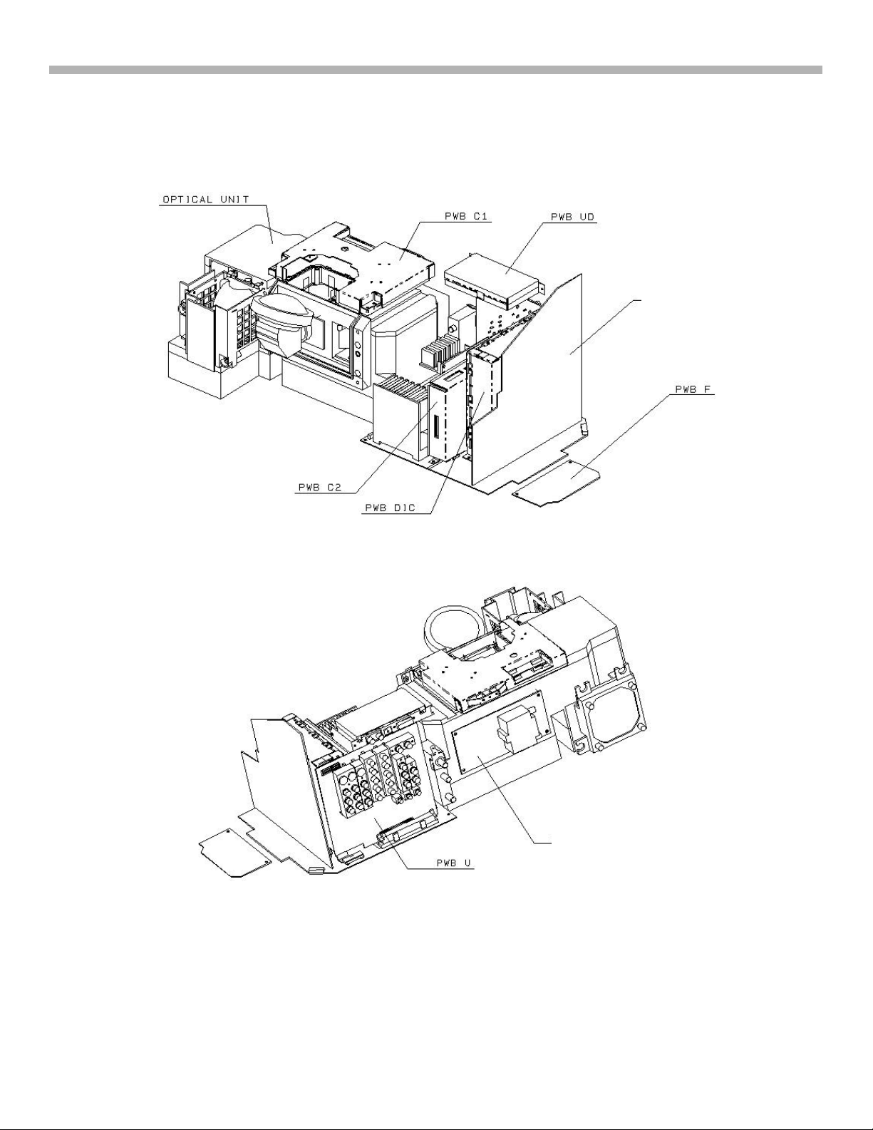
1. The LA-2 Chassis
PWB G1
Circuit Board Locations
Figures 1-2A and 1-2B illustrate the locations of the key circuit boards. The service policy as of this writing is
board-level repair only.
FIGURE 1-2A - CIRCUIT BOARD LOCATIONS
PWB Lamp Driver
FIGURE 1-2B - CIRCUIT BOARD LOCATIONS
6
2. LA-2 Power Supplies
Chapter 2 - LA-2 Power Supplies
Overview
Most of the power sources utilized by the chassis are generated on the G1 board. It is the beginning point of all
power distribution and serves two key functions: It’s purpose is to generate a standby voltage for supplying
power to the Main Microprocessor, IR receiver, SIRCS and the main power relay and to operate the main converter
to develop the necessary secondary voltages to be distributed to the other circuit boards.
The main switching converter is only active when the unit is turned ON and the main relay closes. It supplies
many of the initial voltages to be distributed throughout the unit. Other sub-circuits and regulator devices feed off
these voltages and are spread throughout the unit.
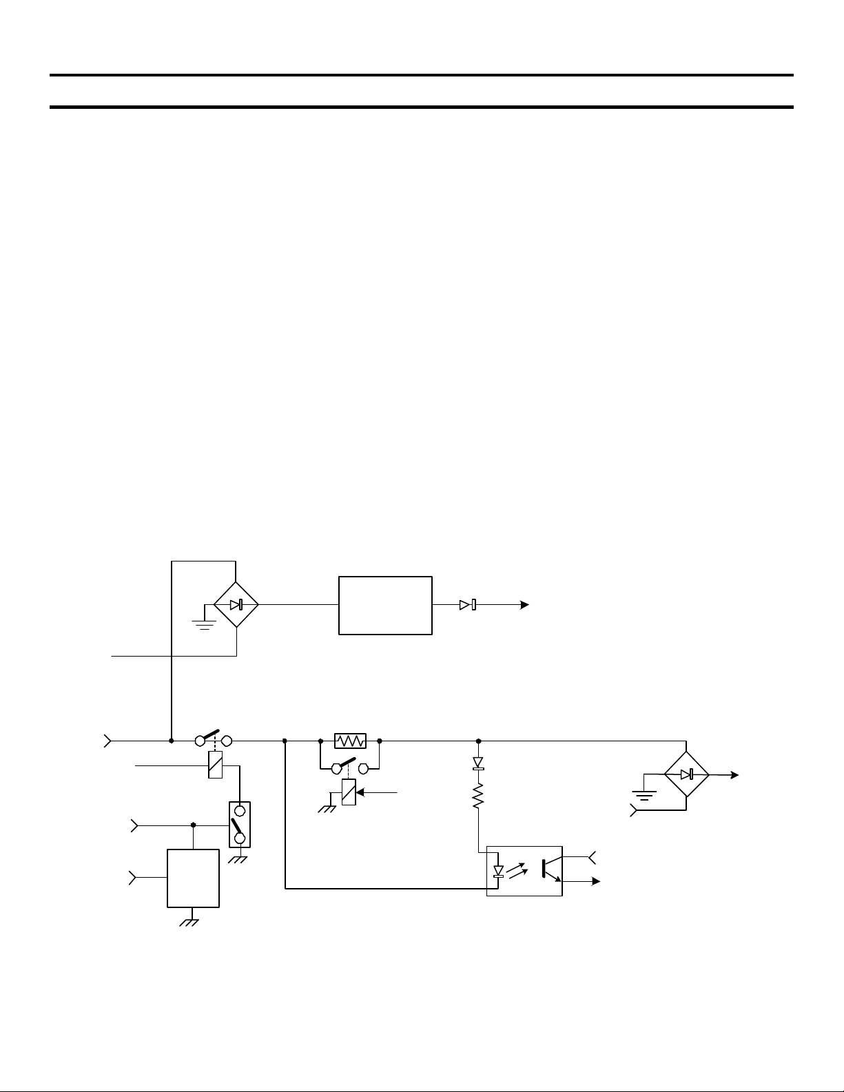
AC Switching and Standby
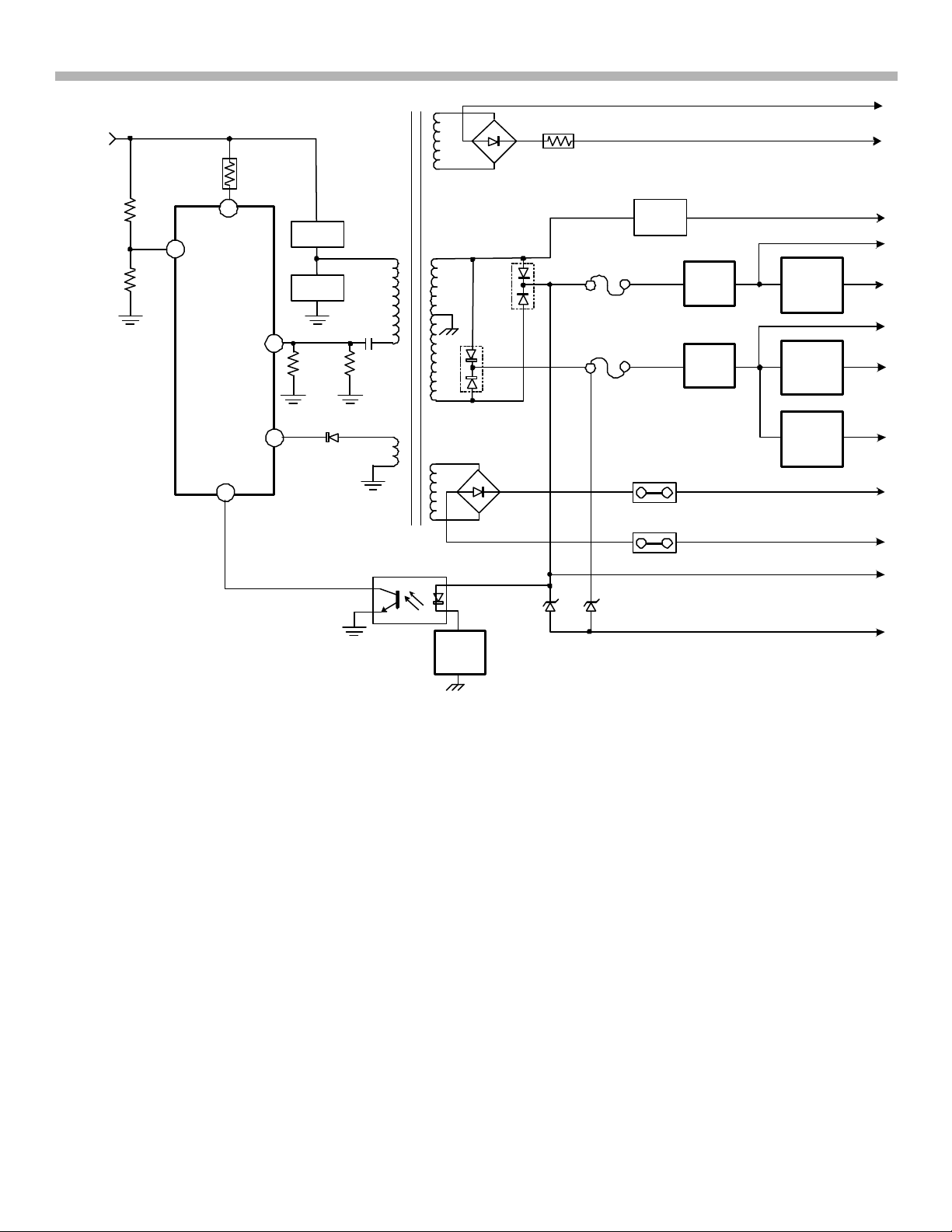
In Figure 2-1, a simplified block of the standby power supply and AC switching is shown. It consists of a simple
single transistor, switched-mode circuit driving a small transformer, T1601 (not shown). D1614 rectifies a 7-volt
line supplying power to the main relay RY1601. It is also applied to additional analog regulators on other boards
to provide STBY 5V for various circuits, particularly the CPU and IR detector.
A logic high entering as PW CTL turns on Q1603. This energizes Main Relay RY1601. Initial current is absorbed
by R1652, a 3.3O, 10-watt resistor to minimize relay arcing. This resistor is rapidly shunted by another relay,
RY1602, which is energized by D6.5V generated by the secondary side of the main converter. If RY1602 fails to
close its contacts, the voltage drop across R1652 will be detected by PH1602 and cause the main converter to go
into protective shutdown by engaging the latch circuit consisting of Q1605 and Q1605. The energizing of RY1602
is an important tool to determine if the main converter is operational and this will be covered in the troubleshooting
section later in this chapter.
AC H
AC L
SUB 7V
PWCTL
PROTECT
RY1601
Q1603
Q1604
Q1605
LATCH
D1601
STBY
SWITCHING
SUPPLY
R1652
3.3 10W
RY1602
IN-RUSH
CURRENT
D6.5V
SUB 7V
D1614
D1648
R1701
PH1602
FIGURE 2-1 - LA-2 AC SWITCHING & STANDBY
D1602
RECT
AC
AC H
11V
PROTECT
LATCH
TVP17.2-1 1/14/04
7

2. LA-2 Power Supplies
Main Converter
In Figure 2-2, the main converter circuits operate to generate most of the essential voltages used by the unit.
IC1601 is a high-frequency switching regulator that will drive a pair of switching transistors (Q1606 and Q1607).
These transistors drive the primary windings of T1603. Q1606 sends current into the primary, exits through
C1629 and on to ground potential via R1618 and R6138. When Q1606 turns off, Q1607 conducts to dissipate
the energy in the primary windings and discharge C1629 for the next cycle.
IC1601 must be started to begin its function. A voltage is applied to pin 18 (VD) through R1607 and another
voltage to pin 1 (V SENSE) via a resistor divider network. This sense line is to monitor the incoming rectified AC
and protect against low voltage. It is approximately 2.5VDC at 120VAC input. If it falls to 1.5VDC or less, the
oscillator inside IC1601 will stop. If the voltages at pins 1 and 18 are present and have the proper level, the IC will
begin sending drive pulses to the switching transistors. The drive pulses are square-wave with a constant 50%
duty cycle. Only the frequency of the square wave will vary to control regulation.
In order for IC1601 to continue running, a voltage of approximately 15VDC must be present at pin 8 (VC1). This
is supplied by a sample winding from T1603 and rectifier D1609. If this VC1 voltage does not appear, IC1601 will
produce four attempts of drive pulse bursts to the switching transistors before finally shutting down.
Regulation
There are two 17-volt sources generated by the secondary stage of the main converter. The 17V-1 line is
monitored by the LED anode inside PH1601. The cathode of the LED is held at reference by IC1602. Any rise
in the monitored voltage will cause the LED to light more and the transistor inside PH1601 to conduct more. The
voltage at pin 2 (FB) will drop and cause the oscillator inside IC1601 to increase in frequency and reduce the
secondary voltages. The opposite sequence of events will occur if the 17V line should decrease.
Should the regulator fail to maintain control, both 17V lines are monitored by D1619 and D1639. Both Zener
diodes are rated at 18V. If either or both of the 17V lines rise to 18V or above, the main relay latch circuit will
activate, shutting the unit down
Secondary Voltages
Bridge rectifier D1608 supplies approximately 250VDC and is dedicated to the lamp driver power supply. Q1613
and Q1622 form a voltage pump-up circuit to generate 33VDC for the tuner. AU+17V and AU-17V from D1624
are dedicated to the audio circuits. All voltages generated on the G1 board are sent via CN1603 to CN8902 on
the A board where they will be either used or passed on to other circuit boards.
8
REC AC
FROM
D1602
R1624
N1626
V SENSE
R1629
18
1
IC1601
SWITCHING
REGULATOR
R1607
9
Q1606
Q1607
R1618
C1629
R1638
D1624
D1608
R1613
D1623
F1602
4A
F1603
4A
DC-DC
CONV
Q1613
Q1622
2. LA-2 Power Supplies
LAMP GRND
LAMP PWR
IC1603
IC1604
IC1608
+9V
REG
IC1606
+5V
REG
+33V
+11V
+9V
+5V
D1609
8
VCI
D1624
2
PS1601
IC1609
+4V
REG
+4V
AU +17V
2.5A
PH1601
D1619
17V OVP1
PS1602
2.5A
D1639
17V OVP2
TO RELAY LATCH
AU -17V
17V DET
IC1604
FIGURE 2-2 -LA-2 MAIN POWER SUPPLY
TVP17.3 1/16/04
9
2. LA-2 Power Supplies
Troubleshooting
Although service policy dictates board-level troubleshooting, it still becomes necessary to perform some tests
and diagnostics to isolate a potential failure to the G1 board. The possibility of unavailable replacement
boards in the future may require troubleshooting down to component level. Figures 2-3 and 2-4 contain
flowcharts to assist in guiding you to the probable cause of a unit that will not turn on.
START
STBY/POWER
LED ON FRONT
PANEL LIT?
YES
RELAY CLICK
HEARD?
YES
NO
NO
RY1601 OR
RELAY DRIVE
7VDC AT D1614
CATHODE ON
G1 BOARD?
YES
5VDC AT IC8008
PIN 8 ON A
BOARD?
YES
NO
NO
STANDBY
SUPPLY
FAILURE
STBY 5V REG
IC8008 NG
RY1602
ENGAGING?*
*USE FINGER
TO DETECT
NO
GO TO CONVERTER
TROUBLESHOOTING
ACTION OF
YES
RELAY
CONVERTER OK
CHECK FOR MISSING
SECONDARY
VOLTAGE
5VDC AT CN8020
PIN 2?
YES
REPLACE C2
BOARD
FIGURE 2-3 - DEAD SET TROUBLESHOOTING FLOWCHART
10
TVP17.2-3 12/18/03
START
2. LA-2 Power Supplies
APPROX 290VDC
AT IC1601
PIN18?
NO
R1607 OPEN
FAILED IC1601
LIKELY CAUSE
YES
2.5VDC AT
IC1601 PIN 1?
>1.5VDC OR
< 7VDC?
NO
YES
150 ~160VDC AT
IC1601 PIN 16?
NO
IC1601
DEFECTIVE
CHECK R1607
YES
C1629
DEFECTIVE
CHECK FOR LOW
VOLTAGES AT
SECONDARY LINES
TO CONFIRM
DEFECTIVE C1629
RESISTOR
DIVIDER
NETWORK
FIGURE 2-4 - MAIN CONVERTER TROUBLESHOOTING FLOW CHART
TVP17.2-4 12/18/03
11

3. LA-2 Protect and Self-Diagnostics
Chapter 3 - LA-2 Protect and Self-Diagnostics
Overview
The LA-2 chassis utilizes several circuits to monitor various conditions during the operation of the unit for safety
and reliability, along with providing diagnostics indicators to assist both the customer and the technician in
understanding what the problem might be. Excessive voltages, current and operating temperatures are some
examples. Protection can involve the simple task of shutting down the unit completely to protect other circuits or
simply to notify of a problem such as a failed lamp.
Roughly half of the protect monitoring circuits can shut the unit down without any visible diagnostics indicators,
while the other half will attempt to display the problem by flashing the lamp or timer LED on the front panel. Any
event that flashes the timer LED will also store the event into a diagnostics page that can be called up for
analysis providing the unit is able to turn on and display a picture. This will be covered later in this chapter.
Although the unit is considered board-level only repair, it is important to isolate the cause of a protect circuit
event, whether or not a diagnostics indication is displayed, so the proper board can be replaced to remedy the
problem.
The following diagrams will be discussed showing the protect circuits not associated with self-diagnostics followed
by those monitored for diagnostics display. Most protection events not monitored will directly turn off the relay
drive. Some will instruct the main microprocessor to turn the unit off. All protect circuits that are part of the selfdiagnostics feature are monitored and activated by the main microprocessor located on the C2 board.
Direct Relay Deactivation Protection
Description
In Figure 3-1 there are several protect lines shown directly tied to the relay latch circuit and all except for the
MS3.3V OVP are located on the G1 board. All of the lines are isolated by diodes and a high from any one of them
will turn on Q6105, pulling down the “high” command from PWCTL. The base of PNP transistor Q1604 will also
be pulled low, turning it ON and feeding the remaining pull-up voltage to latch the circuit. The microprocessor will
continue to send the high command. This is why the unit must be turned off to release the latch before it can be
turned ON again.
As can be seen, all of the protection circuits except for one are monitoring for excessive voltages. 11V, D6.5V,
17V-1 and 17V-2 are generated by the secondary lines of the main power supply. MS3.3V IC8009 is located on
the A board.
PH1602 is monitoring for a failure of inrush current relay RY1602. If this relay does not close, excessive heating
of R1652 will occur along with potential damage to the main converter due to large current fluctuations. The
voltage drop across R1652 will light the LED inside PH1602, causing the phototransistor to conduct and send a
high to D1647. One would always expect a spike of voltage across R1652 during initial turn-on but C1620 at the
base of Q6105 will delay the activation of the latch circuit to prevent any random transient voltage fluctuations
from accidentally tripping it
12
R1652
3.3 10W
3. LA-2 Protect and Self-Diagnostics
AC L
R1623
PWCTL
Troubleshooting
SUB 7V
R1622
Q1605
C1620
10V
RY1601
R1621
Q1604
R1630
IC8009
MS 3.3
Q1603
D8035
RY1602
D1647
D8306
FIGURE 3-1 - LA-2 PROTECT-1
D6.5V
11V
PH1602
D1640
D1642
D1618 D1619
D1638 D1639
B+
D1647
R1701
D1641
11V
D1641
D6.5V
17V-1
17V-2
TVP17.3-1 1/16/04
Obviously, any of the previous protect circuits will shut the unit down without providing diagnostics indications.
The first item to pay attention to is the clicking of the main relay. If you do not hear a click, there is not a protect
event occurring. Two relay clicks (main relay turned on, then off), is a clear indication of a protect event.
As mentioned earlier, there are other protect circuits on the C board that can tell the microprocessor to shut the
unit down without diagnostic indications. Here is a tip to quickly tell if one of the lines on the G1 board is the
cause:
If you have to turn the unit off with the remote or the power button to get it to turn back on, one of the lines on
the G1 board has activated the latch.
Troubleshooting now narrows down to determining which isolation diode is being forward-biased into the latch
circuit. Fortunately, this particular design does not have the blocking diodes directly connected to the base of
Q1605. Otherwise, a peak-hold meter would be needed to capture the 0.6V, which is the maximum level at the
base of a straight bi-polar transistor with the emitter grounded. Since R1630 is in series with the base, rather
large voltage levels will appear at the cathode of any blocking diode whose monitoring circuit is “firing” into its
anode. Placing a DVM at the anode of each blocking diode will expose the source of the shutdown.
For example: If the 11V rose sufficiently to fire zener diode D1641, most of the voltage would pass through
D1640 and on to R1630. Even a DVM without peak-hold placed on the anode of D1640 would be able to pick up
this event before the latch circuit engaged.
13

3. LA-2 Protect and Self-Diagnostics
Protection and Self-Diagnostics
Description
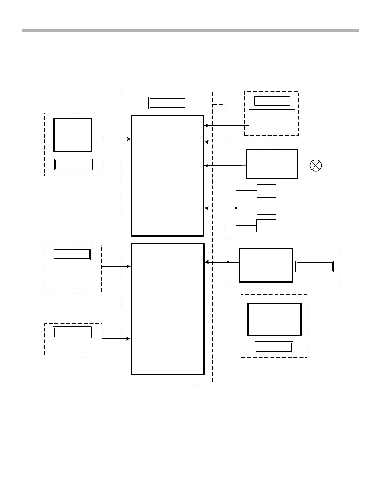
Figure 3-2 illustrates how the Main and LCD Engine microprocessors located on the C2 board monitor the other
important circuits in the unit. All of the listed monitoring lines will cause the unit to power down by removing the
relay “high” command (PWCTL) to the main relay driver on the G1 board. The particular event that triggered the
protection will also cause the timer or lamp LED to flash. The lamp LED will only flash if a lamp failure is sensed.
The timer LED will flash in designated sequences. As an example: If excessive temperature is detected by IC47
on the H3 board, the unit will power down and the timer LED will flash four times at 500ms intervals followed by
a two second separation period and another set of four flashes and so on. The event will also be stored into a
NVM IC on the C2 board for viewing if necessary. Below is a brief description of each protect item:
TEMP: A digital thermometer (IC47) located on the H3 board monitors ambient temperature within the cabinet of
the unit. The IC communicates with IC3208 via the I²C bus. Once the temperature has exceeded acceptable
limits the unit will power down and the timer LED will flash in sequences of four.
OVP: There is a power board known as the G3 board that is an integral part of the DIC2 board. It outputs a 3.3V,
2.5V and 1.8V source. If either exceeds specified voltage levels, a high is sent to IC3405. The LED flash
sequence will be eight times.
17V OVP: Although the 17V lines on the G board are monitored by zener diodes to activate the protect latch, the
17V-1 is redundantly monitored here to provide the only diagnostics indication from a G1 board protection. The
LED will flash six times.
Speaker DC Detect : To prevent damage to the speakers if one of the amplifiers should short and place DC onto
the lines, both the main L/R amp (IC47) on the AU board and the woofer amp (IC85) on the A board are monitored.
Any DC voltage will send a high to IC3405. The LED will flash seven times.
Fan Protect: Although the schematic shows five fan drivers, only three fans are used in this model. All are
located in the lamp and optical assemblies. When the fans are rotating normally, a low is output from the protect
line of each. If one or more fail to rotate, a high will be sent to IC3208. The LED will flash four times.
Lamp Cover Switch : When the lamp cover is closed, a switch (S3999 on the T board) grounds this line. If the
cover is not closed or the switch fails, a high is sent to IC3208. The LED flashes three times.
Lamp Detect: A high-pressure, mercury vapor arc lamp is used. As the lamp ages the arc gap increases.
Current draw will decrease and when this threshold is reached, the lamp LED will flash, notifying it is time to
replace the lamp.
14
3. LA-2 Protect and Self-Diagnostics
IC47
TEMP
SENSE
H3 BOARD
*G3 BOARD PART OF
DIC2 BOARD
G3 BOARD*
+3.3V
+2.5V
+1.8V
OVP
4X
8X
C2 BOARD
TEMP
LCD ENGINE
D-0VP
IC3208
MICRO
LAMP
SW
LAMP
PWR
LAMP
FAN
SP
PROT
7X
3X
5X
LAMP
LED
T BOARD
LAMP COVER
SWITCH
LAMP POWER
BLOCK
FAN 1
4X
FAN 2
FAN 3
IC85
SPEAKER
DC DETECT
A BOARD
G1 BOARD
I7V 0VP
6X 17V
OVP
FIGURE 3-2 - LA-2 PROTECT-2
IC3405
MAIN MICRO
IC47
SPEAKER
DC DETECT
AU BOARD
TVP17.3-2 1/30/04
15
3. LA-2 Protect and Self-Diagnostics
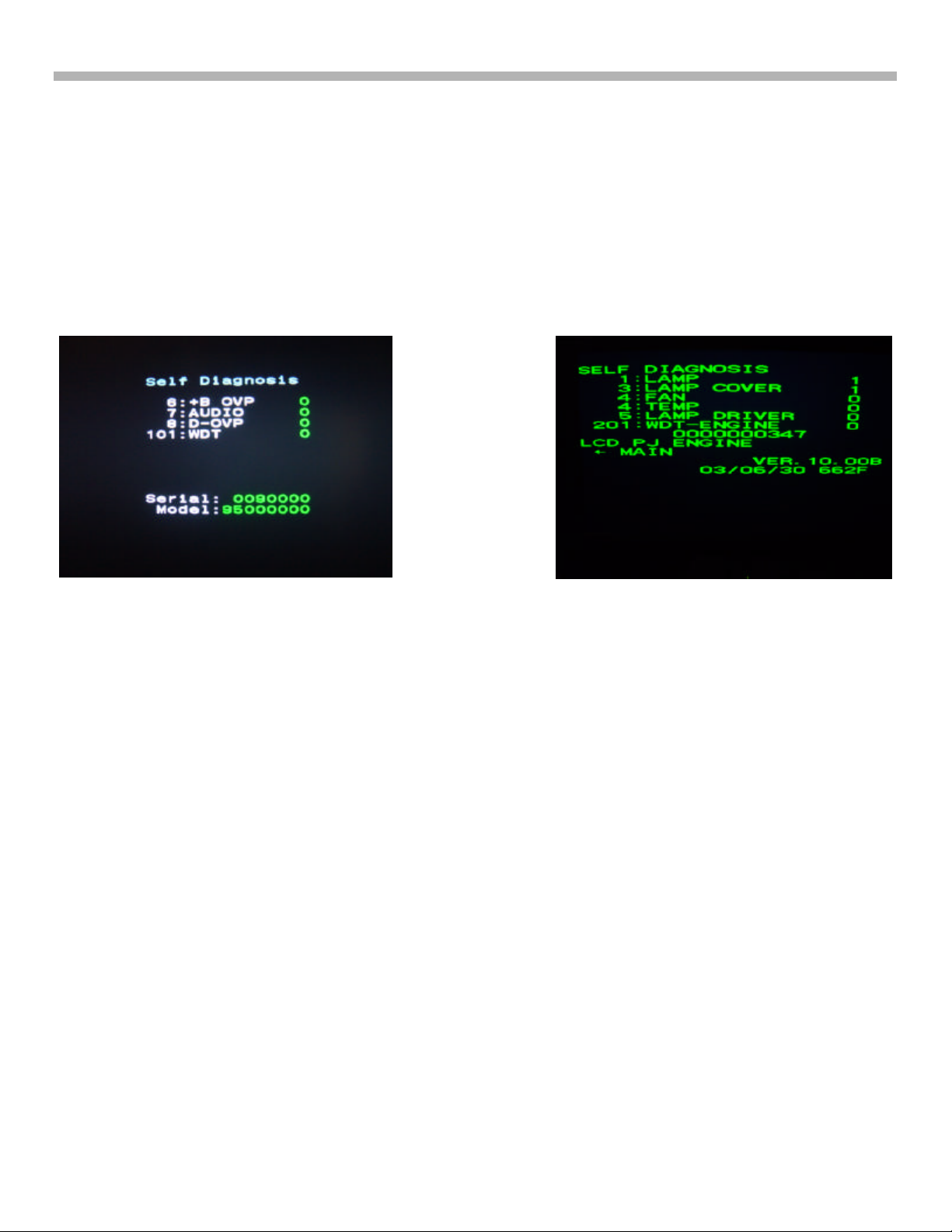
Entering Diagnostics Mode
A failure history of each monitored diagnostics circuit can be viewed by pressing “DISPLAY”, “5”, “VOLUME –”
and “POWER” on the remote commander. Unlike previous versions of this feature, the failure history is split
between two pages. By using the left/right command on the remote joystick, you can toggle between them. This
is shown in Figure 3-3. The initial page displayed is generated by the main microprocessor on the C2 board and
is the same RGB line generating the customer menu. The second page displaying the remaining list is generated
by the service mode OSD. This is generated by the LCD engine microprocessor (also located on the C2 board)
and is only displayed in green.
The diagnostics display is useful for viewing past failure events to isolate causes of intermittent shutdown events.
It is important to clear the event count before exiting this mode. This is accomplished by pressing “8” and
“ENTER” on the remote.
< >
JOYSTICK
FIGURE 3-3 - LA-2 SELF-DIAGNOSTICS
TVP17.3-3
1/16/04
16

4. LA-2 Video Processing
Chapter 4 - LA-2 Video Processing
Overview
The LA-2 chassis utilizes three LCD panels to project an image onto a 16:9 ratio screen. A high-pressure arc
lamp generates the light, which is then passed through dichroic mirrors to separate and divert the white light into
red, green and blue. Each color is passed through sets of polarizing filters, allowing only one plane of light to
pass through the LCD panels. The three images generated by the LCD panels are mixed and passed through a
single lens to a mirror and onto the rear of the screen assembly.
The LA-2 chassis used in the WE610 model series is classified as a “high definition ready” television. A true high
definition television must contain a tuner capable of receiving terrestrial ATSC digital television broadcasts along
with the necessary decoder circuits to de-compress MPEG2 video and PCM or Digital Dolby® audio. The LA-2A
chassis used in the XBR950 series contains these items in what is known as the “Q box” and is, therefore, a true
high definition television. This new tuner will be able to receive and decode QAM signals used by the cable
companies along with VSB used by terrestrial broadcasters.
In either case, each model must be able to receive a multitude of video formats and resolutions. Soon-to-be
legacy NTSC video must be processed to increase the resolution and quality to maintain a reasonable appearance
on high-resolution display devices such as those found on this chassis. These signals are available in three
different analog formats: Composite, S-Video and Component. There are also a number of resolutions supported
by the ATSC specifications. All ATSC formats are digital and, therefore, require less circuitry to increase resolution
if needed.
Encoded analog video signals must be decoded before being processed by digital circuits. Examples of encoding
are synchronization pulses and chroma carrier signals. These are necessary to lock a receiving device to a
transmitting device but are not required when processed internally by a display device. The analog to digital
conversion performed by multi-format devices such as this chassis requires sampling all of the portions of a
particular analog signal, and since the encoding portions are not required, large amounts of bits would be allocated
to unnecessary information. This is why composite and S-Video signals are decoded to component level.
Since this chassis is capable of receiving a broad spectrum of video formats and resolutions, a rather complicated
array of switching, routing and processing of video signals is performed before being sent to the LCD display
panels. This can be utilized to one’s advantage when troubleshooting video problems and will be covered later
in this chapter. Digital processing and the use of a light source rather than conventional CRT scanning can
produce failure symptoms that are new to veteran technicians. Consequently, a fresh, new approach to analyzing
what appears on the display screen is required to properly diagnose the potential problem area of a failure. The
same rule applies as did with CRT displays: The screen is your most powerful piece of test equipment.
Video Input and Switching
As mentioned earlier, the many available sources and resolutions of video signals has necessitated the need for
many input sources on today’s high-end televisions. In Figure 4-1, the various signal sources and switching of
those signals is defined. Ten different sources of video are available for selection by the customer. Six are
limited to NTSC broadcast quality 480i sources (main and sub tuner and video 1 through 4), two to non-broadcast
NTSC 480i and ATSC resolutions of 480i to 1080i (video 5 and 6), one to ATSC signals only (video 7) and one to
JPEG and MPEG1 still images and video (memory stick).
All input sources from the tuners and video 1 to 4 inputs are selected by A/V switches IC9400 and IC9401,
located on the U board. Both switchers are capable of selecting any two of the aforementioned inputs, outputting
them as main and sub video. Selected sub video is sent to the DIC2 board for processing and can be either
composite or Y/C, depending on the source selected.
Main video exits IC9401 and enters Video Switch IC9404. The purpose of this IC is to allow the insertion of video
content from the video 5, 6 and 7 inputs as main video. The reason for this procedure is as follows: Any video
17
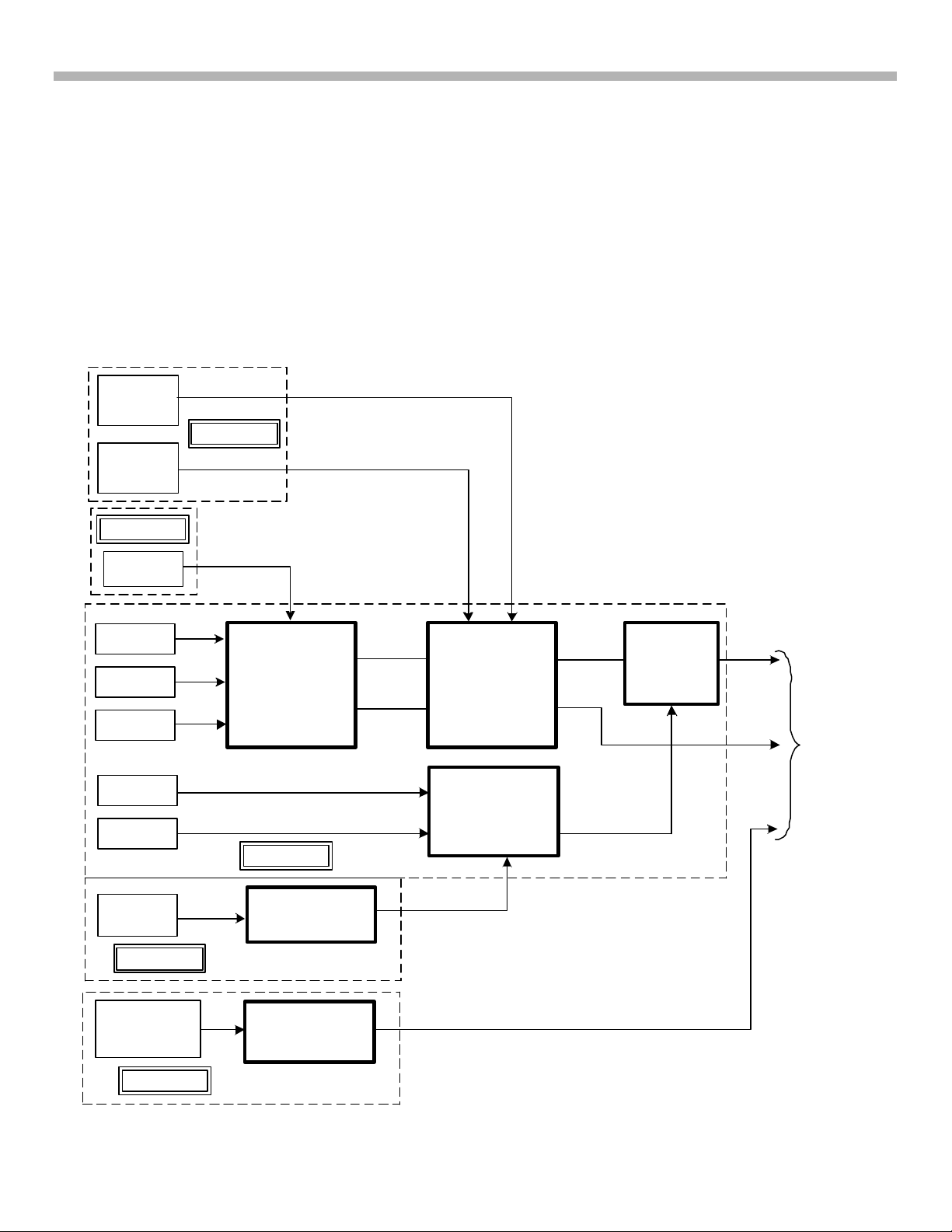
4. LA-2 Video Processing
source received from the tuners or video 1 through 5 will always be 480i material. These resolutions must be
processed by the DRC (Digital Reality Creation) to double the line count (480i to 960i) and the horizontal resolution
(720 to 1440) to increase picture quality. The MID (Multi-Image Driver) accepts two video sources for side-byside, or Twin View, display. One of these inputs comes from the DRC. The other receives video directly and can
accept any resolution. The DRC cannot process video resolutions above 480i. Any video source above 480i is
always routed through the main path. The sub path can only process 480i. Whenever Twin View is selected and
the main video source is higher than 480i, it will always appear on the left side of the screen. If an active sub
video source is present, it will appear on the right. The two video sources cannot be swapped. If both video
sources are 480i, they can be swapped.
Component video sources from input 5, 6 and 7 are selected by IC9402 and sent to IC 9404 for insertion into the
main path. The DVI input must be converted to analog component and this is accomplished by IC7004 on the
UD board, which also contains the DVI connector.
JPEG and MPEG1 images and video are sent directly to the DIC2 board for processing.
MAIN
TUNER
A BOARD
SUB
TUNER
H3 BOARD
VIDEO 2
VIDEO 1
VIDEO 3
VIDEO 4
VIDEO 5
VIDEO 6
VIDEO 7
DVI
UD BOARD
IC9400
AV SW1
U BOARD
IC7004
DVI I/F
MAIN
SUB
IC9402
AV SW2
IC9402
COMPONENT
SWITCH
MAIN
SUB
I C904
VIDEO
SWITCH
TO DIC2
BOARD
MEMORY
STICK
SLOT
HM BOARD
IC1301
LVDS
TRTX
FIGURE 4-1 - LA-2 VIDEO SWITCHING
18
TVP17.4-1 1/16/04
 Loading...