

Page 1
SERVICE MANUAL
MODEL
.............. ......... ....................
DEST. CHASSIS NO. MODEL DEST. CHASSIS NO.
VPL-CS5 WORLD
VPL-CX5 WORLD
.............. ......... ....................
RM-PJM12 WORLD
DATA PROJECTOR
Page 2

! WARNING
This manual is intended for qualified service personnel only.
To reduce the risk of electric shock, fire or injury, do not perform any servicing other than that
contained in the operating instructions unless you are qualified to do so. Refer all servicing to
qualified service personnel.
! WARNUNG
Die Anleitung ist nur für qualifiziertes Fachpersonal bestimmt.
Alle Wartungsarbeiten dürfen nur von qualifiziertem Fachpersonal ausgeführt werden. Um die
Gefahr eines elektrischen Schlages, Feuergefahr und Verletzungen zu vermeiden, sind bei
Wartungsarbeiten strikt die Angaben in der Anleitung zu befolgen. Andere als die angegeben
Wartungsarbeiten dürfen nur von Personen ausgeführt werden, die eine spezielle Befähigung
dazu besitzen.
! AVERTISSEMENT
Ce manual est destiné uniquement aux personnes compétentes en charge de l’entretien. Afin
de réduire les risques de décharge électrique, d’incendie ou de blessure n’effectuer que les
réparations indiquées dans le mode d’emploi à moins d’être qualifié pour en effectuer d’autres.
Pour toute réparation faire appel à une personne compétente uniquement.
WARNING!!
AN INSULATED TRANSFORMER SHOULD BE USED DURING
ANY SERVICE TO AVOID POSSIBLE SHOCK HAZARD, BECAUSE OF LIVE CHASSIS.
THE CHASSIS OF THIS RECEIVER IS DIRECTLY CONNECTED
TO THE AC POWER LINE.
SAFETY-RELATED COMPONENT WARNING !!
COMPONENTS IDENTIFIED BY A
DIAGRAMS, EXPLODED VIEWS AND IN THE PARTS LIST ARE
CRITICAL TO SAFE OPERATION. REPLACE THESE COMPONENTS WITH SONY PARTS WHOSE P ART NUMBERS APPEAR
AS SHOWN IN THIS MANUAL OR IN SUPPLEMENTS PUBLISHED BY SONY .
!!
! MARK ON THE SCHEMA TIC
!!
ATTENTION!!
AFIN D’ÉVITER TOUT RISQUE D’ÉLECTROCUTION
PROVENANT D’UN CHÂSSIS SOUS TENSION, UN
TRANSFORMA TEUR D’ISOLEMENT DOIT ETRE UTILISÉ LORS
DE TOUT DÉPANNAGE.
LE CHÂSSIS DE CE RÉCEPTEUR EST DIRECTEMENT
RACCORDÉ Á L’ALIMENTATION SECTEUR.
ATTENTION AUX COMPOSANTS RELATIFS Á LA
SÉCURITÉ!!
LES COMPOSANTS IDENTIFIÉS PAR UNE MAPQUE
LES SCHÉMAS DE PRINCIPE, LES VUES EXPLOSÉES ET LES
LISTES DE PIECES SONT D’UNE IMPORTANCE CRITIQUE
POUR LA SÉCURITÉ DU FONCTIONNEMENT. NE LES
REMPLACER QUE PAR DES COMPOSANTS SONY DONT LE
NUMÉRO DE PIÈCE EST INDIQUÉ DANS LE PRÉSENT
MANUEL OU DANS DES SUPPLÉMENTS PUBLIÉS P AR SONY.
!!
! SUR
!!
VPL-CS5/CX5
Page 3

For the customers in the Netherlands
Voor de klanten in Nederland
Hoe u de batterijen moet verwijderen, leest u in de tekst
van deze handleiding.
Gooi de batterij niet weg maar lever deze in als klein
chemisch afval (KCA).
Für Kunden in Deutschland
Entsorgungshinweis: Bitte werfen Sie nur entladene
Batterien in die Sammelboxen beim Handel oder den
Kommunen. Entladen sind Batterien in der Regel dann,
wenn das Gerät abschaltet und signalisiert “Batterie
leer” oder nach längerer Gebrauchsdauer der Batterien
“nicht mehr einwandfrei funktioniert”. Um
sicherzugehen, kleben Sie die Batteriepole z.B. mit
einem Klebestreifen ab oder geben Sie die Batterien
einzeln in einen Plastikbeutel.
VPL-CS5/CX5
1 (P)
Page 4

Page 5

Table of Contents
1. Service Information
1-1. Board Layout...............................................................................................1-1
1-2. Disassembly ................................................................................................1-2
1-2-1. Top Panel Assy Removal ...........................................................1-2
1-2-2. Side Panel Assy and L, NR, H2, Q Boards Removal ................ 1-2
1-2-3. Power Block (Lamp) Removal...................................................1-3
1-2-4. DC Fan Removal ........................................................................ 1-3
1-2-5. Lens Gear Removal .................................................................... 1-4
1-2-6. Speaker Assy and DC Fan (Sirocco) Removal .........................1-4
1-2-7. C Board Removal .......................................................................1-5
1-2-8. MSC and MS (VPL-CX5) Boards Removal ..............................1-5
1-2-9. GA and GB Boards Removal .....................................................1-6
1-2-10. Optics Block Assy and Lamp Assy Removal ............................ 1-7
1-2-11. PS Com Aperture and In-polarizer (R), (G), (B) Removal ........1-8
1-2-12. Lens Projection Assy and Lamp Duct Assy Removal ............... 1-9
1-2-13. Prism Block Assy and
Out-pre-polarizer (R), (G), (B) Removal .................................1-10
1-2-14. DC Fan (Sirocco) and V Board Removal ................................1-11
1-2-15. Adjustor Unit Removal ............................................................ 1-11
1-2-16. Extension Board and Extension Connectors ............................1-12
1-2-17. Extension Board and Extension Connectors Connection.........1-13
1-2-18. Warning on Power Connection ................................................1-14
2. Electrical Adjustments
2-1. Preparation ..................................................................................................2-1
2-1-1. Required Equipment...................................................................2-1
2-1-2. Optical Unit Adjustment ............................................................2-1
2-1-3. How to Enter the Factory Mode ................................................. 2-2
2-2. V COM Adjustment ....................................................................................2-2
2-3. Initial Values of Adjustment Items ............................................................. 2-3
2-4. Service Know-How ..................................................................................... 2-8
2-4-1. When the Prism Block Is Replaced............................................2-8
2-4-2. When the C Board Is Replaced .................................................. 2-8
2-5. White Balance Adjustment .........................................................................2-8
2-5-1. HIGH Mode of INPUT-A .......................................................... 2-8
2-5-2. LOW Mode of INPUT-A ...........................................................2-9
2-5-3. HIGH Mode of VIDEO..............................................................2-9
2-5-4. LOW Mode of VIDEO...............................................................2-9
2-6. Memory Structure .....................................................................................2-10
VPL-CS5/CX5
1
Page 6

3. Semiconductors................................................................................. 3-1
4. Spare Parts
4-1. Notes on Spare Parts ...................................................................................4-1
4-2. Exploded Views .......................................................................................... 4-2
4-3. Electrical Parts List ................................................................................... 4-14
5. Block Diagrams
Overall ....................................................................................................................5-1
C (1/4), Q................................................................................................................5-2
C (2/4).....................................................................................................................5-3
C (3/4), H1, H2, L, V, U, NR .................................................................................5-4
C (4/4).....................................................................................................................5-5
MS, MSC ................................................................................................................ 5-6
GA, GB...................................................................................................................5-7
6. Diagrams
6-1. Frame Schematic Diagrams ........................................................................6-2
Frame (1/2) ............................................................................................... 6-2
Frame (2/2) ............................................................................................... 6-3
6-2. Schematic Diagrams and Printed Wiring Boards........................................6-4
Schematic Diagrams
Q................................................................................................................6-4
C (1/10) .....................................................................................................6-6
C (2/10) .....................................................................................................6-7
C (3/10) .....................................................................................................6-8
C (4/10) .....................................................................................................6-9
C (5/10) ...................................................................................................6-10
C (6/10) ...................................................................................................6-11
C (7/10) ...................................................................................................6-12
C (8/10) ...................................................................................................6-13
C (9/10) ...................................................................................................6-14
C (10/10) .................................................................................................6-15
H1............................................................................................................6-20
H2............................................................................................................6-20
L ..............................................................................................................6-22
NR ...........................................................................................................6-22
U..............................................................................................................6-22
V..............................................................................................................6-22
MSC (1/2) ...............................................................................................6-24
MSC (2/2) ...............................................................................................6-25
2
VPL-CS5/CX5
Page 7

MS (1/3) ..................................................................................................6-27
MS (2/3) ..................................................................................................6-28
MS (3/3) ..................................................................................................6-29
GA...........................................................................................................6-31
GB ...........................................................................................................6-34
Printed Wiring Boards
Q................................................................................................................6-5
C .............................................................................................................. 6-16
H1............................................................................................................6-21
H2............................................................................................................6-21
L ..............................................................................................................6-23
NR ...........................................................................................................6-23
U..............................................................................................................6-23
V..............................................................................................................6-23
MSC ........................................................................................................6-26
MS...........................................................................................................6-30
GA...........................................................................................................6-32
GB ...........................................................................................................6-35
VPL-CS5/CX5
3
Page 8

Page 9
1-1. Board Layout
Section 1
Service Information
C
H1
NR
L
MS
(VPL-CX5)
V
H2
MSC
U
Q
Power block (Lamp)
GB
VPL-CS5/CX5
GA
1-1
Page 10
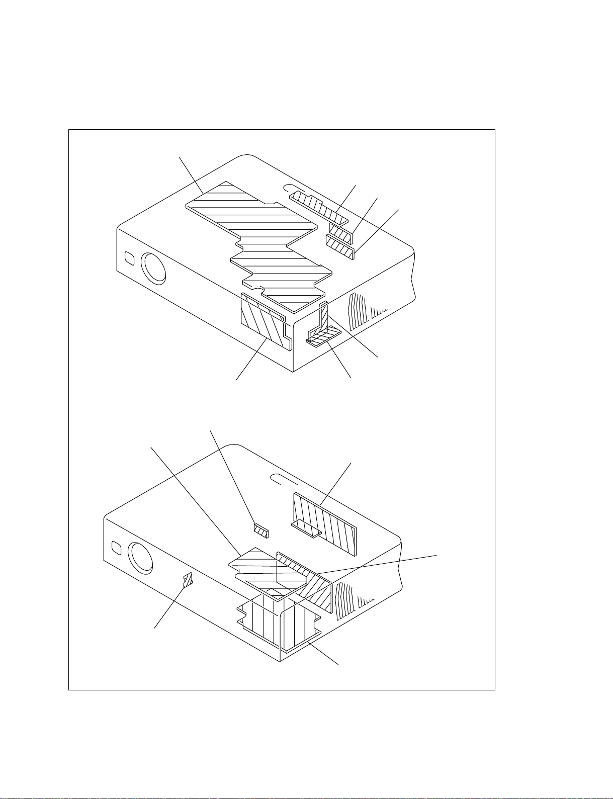
1-2. Disassembly
1-2-1. Top Panel Assy Removal
5 Top panel assy
3 Button (H1) assy
4 H1 board
2 T wo screws
(+B 3 x 6)
1-2-2. Side Panel Assy and L, NR, H2, Q Boards Removal
4 L board
5 NR board
6 Screw
(+B 3 x 6)
CN914
CN915
8 H2 board
CN201
1 Six shafts
3 Side panel assy
7 Button (H2)
2 T wo screws
(+B 3 x 6)
1-2
!- Q board
1 Connector cover
0 Video slee ve
9 Screw
(+B 3 x 6)
VPL-CS5/CX5
Page 11
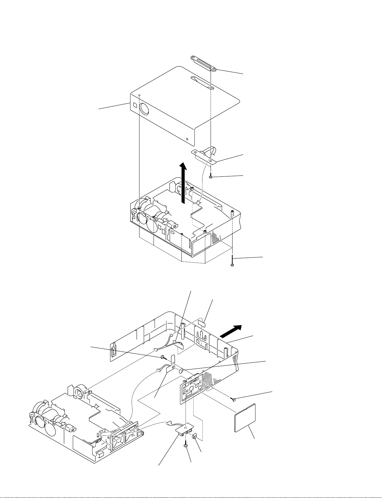
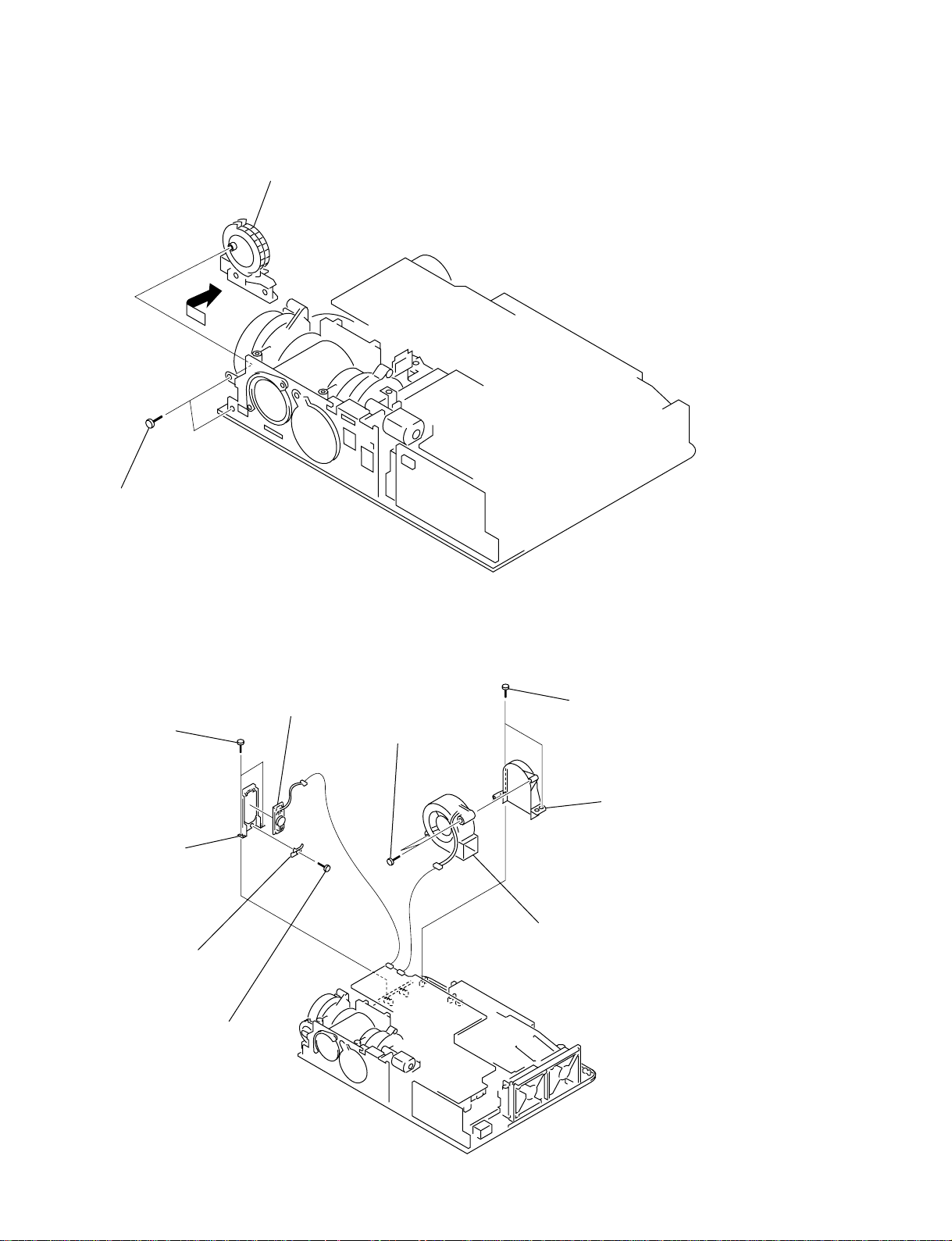
1-2-3. Power Block (Lamp) Removal
1 T wo screws
(+PTPWH 3 x 10)
2 T wo screws
(+B 3 x 6)
CN1
CN907
5 Sheet (LPS)
3 Holder (LPS2)
6 Power block (Lamp)
4 Holder (LPS1)
CN1
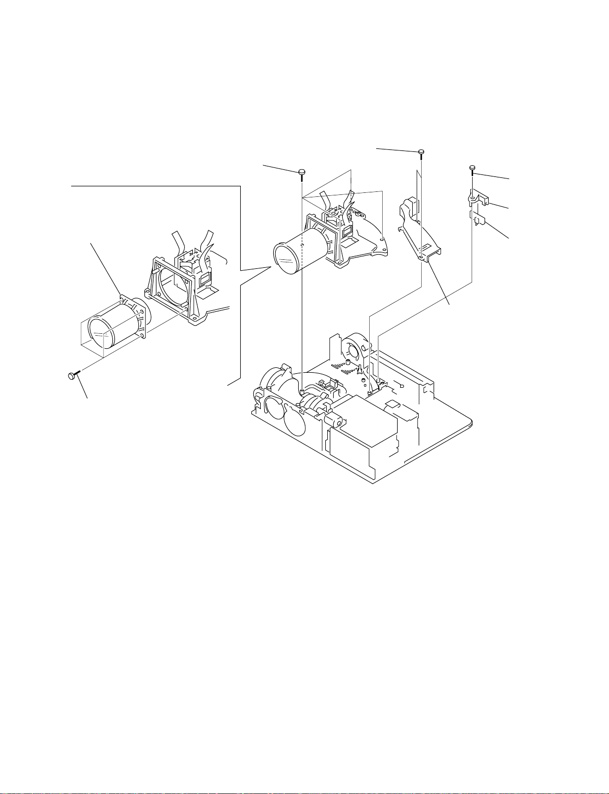
1-2-4. DC Fan Removal
CN909
CN908
1 Screw
(+B 3 x 6)
2 Four screws
(+B 3 x 20)
4 Fan holder (EX)
3 Two DC fans
VPL-CS5/CX5
1-3
Page 12
1-2-5. Lens Gear Removal
2 Lens gear
1 T wo screws
(+BTB 3 x 12)
1-2-6. Speaker Assy and DC Fan (Sirocco) Removal
9 Speaker assy
5 T wo screws
(+B 3 x 6)
CN1102
8 Speaker bracket
7 Speaker holder
6 Screw
(+B 3 x 6)
3 T wo screws
(+BTB 3 x 12)
CN912
1 T wo screws
(+B 3 x 6)
2 Fan (RE) holder
4 DC fan (Sirocco)
1-4
VPL-CS5/CX5
Page 13
1-2-7. C Board Removal
**
* : VPL-CX5
**
1 Three screws
(+B 3 x 6)
CN1102
CN912
CN914
CN907
CN903
2 C board
*
CN701
CN702
CN910
CN911
CN601
CN602
CN901
CN1101
CN501
CN502
*
CN904
CN202
CN913
*
CN909
*
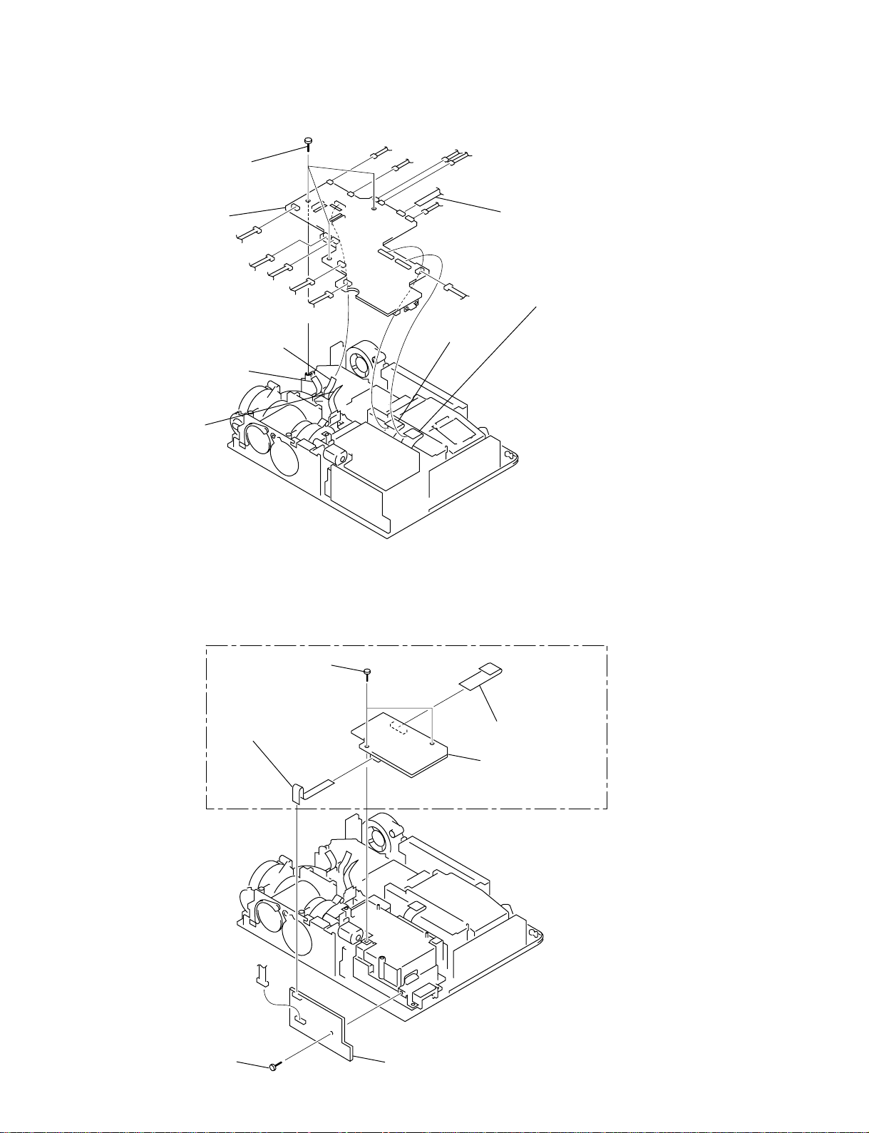
1-2-8. MSC and MS (VPL-CX5) Boards Removal
To remove the MS board, remove the C board beforehand.
Flat connector assy
CN908
CN202 (VPL-CX5)
CN904
(VPL-CX5)
CN1303
1 Screw
(+B 3 x 6)
3 T wo screws
(+B 3 x 6)
Flat connector assy
(12P)
CN1002
CN1301
CN1001
Flat connector assy
(50P)
4 MS board
2 MSC board
VPL-CS5/CX5
1-5
Page 14
1-2-9. GA and GB Boards Removal
To remove the GA and GB boards, remove the C board beforehand.
1 T wo screws
(+B 3 x 6)
2 Screw
(+B 3 x 6)
4 Holder (GA),
Shield (GA)
5 GA board
3 Screw
(+B 3 x 6)
6 Holder GB
CN2001CN2002
CN3501
CN3301
CN3201
7 GB board
Flat connector assy
(24P)
1-6
VPL-CS5/CX5
Page 15
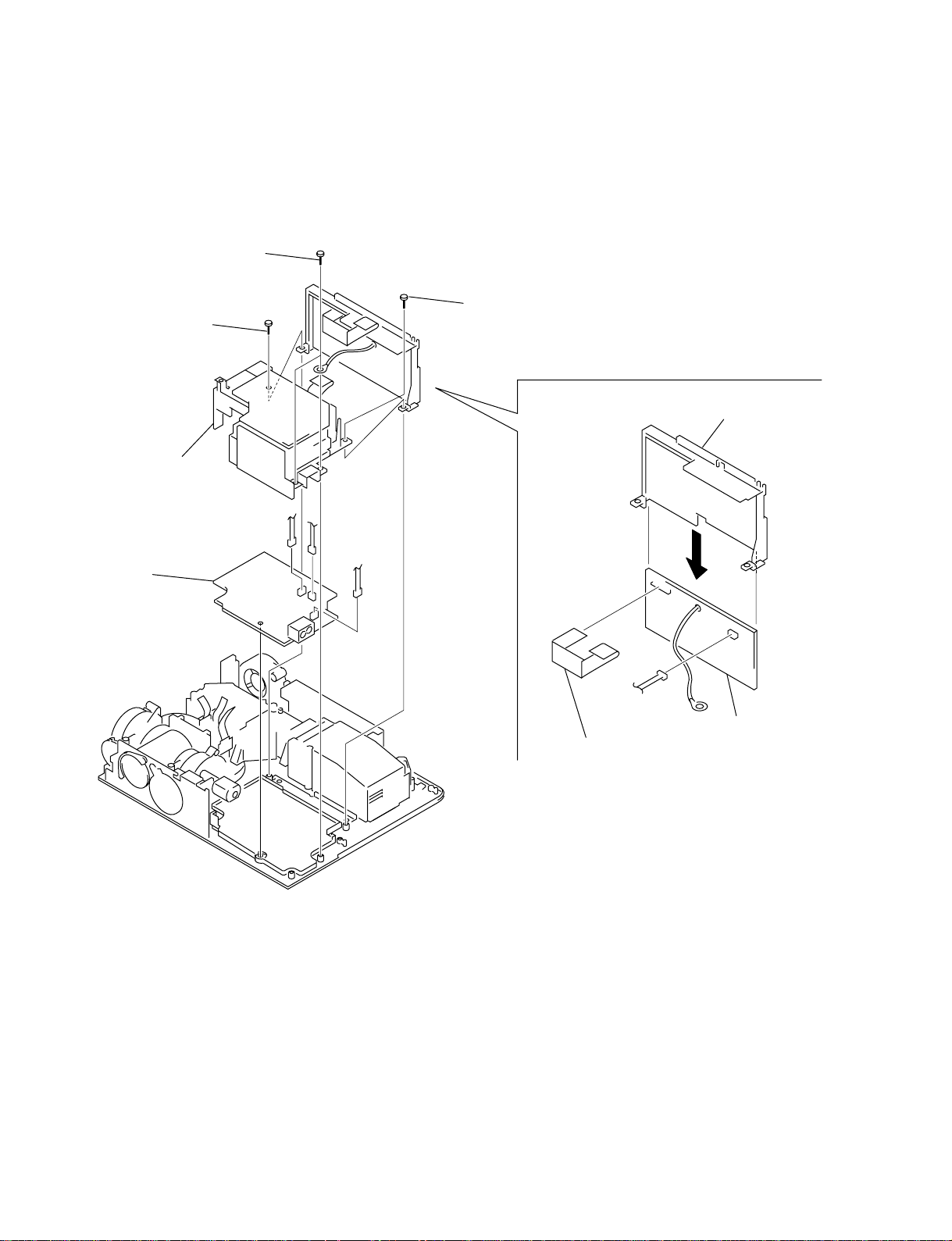
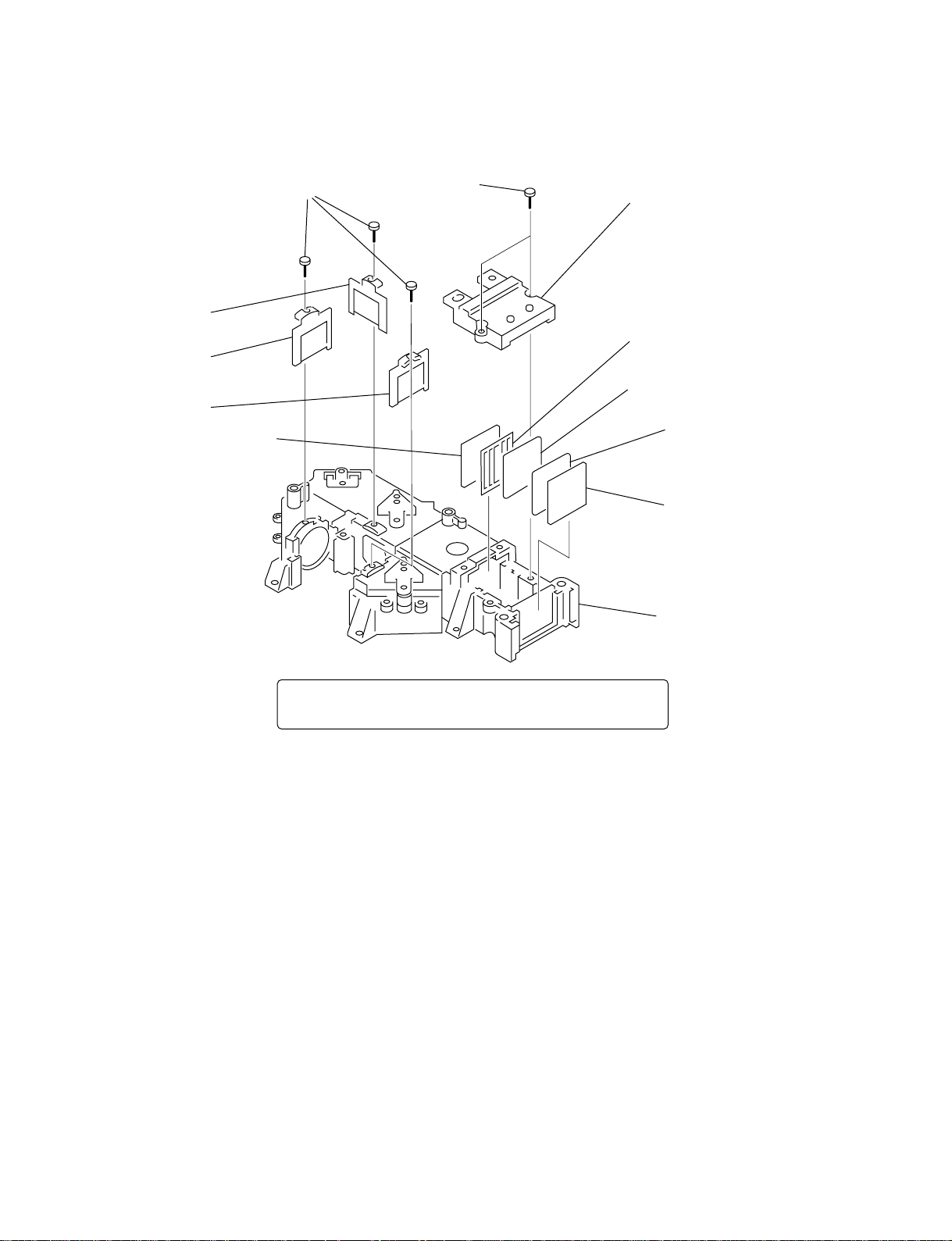
1-2-10.Optics Block Assy and Lamp Assy Removal
4 Four screws
(+)P M4x12
5 Optics block
assy
1 T wo screws
(+PWHTP 3 x 10)
6 Lamp house,
Lamp top cover
2 Connector
(Lamp)
7 Lamp assy
3 T wo screws
(+B 3 x 6)
Optics block assy
To remove the optics block assy and lamp assy, remove the DC fan beforehand.
VPL-CS5/CX5
1-7
Page 16
1-2-11.PS Com Aperture and In-polarizer (R), (G), (B) Removal
9 In-polarizer (G)
0 In-polarizer (R)
!- In-polarizer (B)
5 P/S converter
8 Three screws
(+B 2 x 6)
1 T wo screws
(+B 2 x 6)
2 Unit cover (B), Four cushions
6 PS com aperture
7 Lens-2 fly eye
4 Lens-1 fly eye
3 UV-cut filter
Optics block assy
Note :Do not disassemble the optical block unless
specified by the above views.
1-8
VPL-CS5/CX5
Page 17
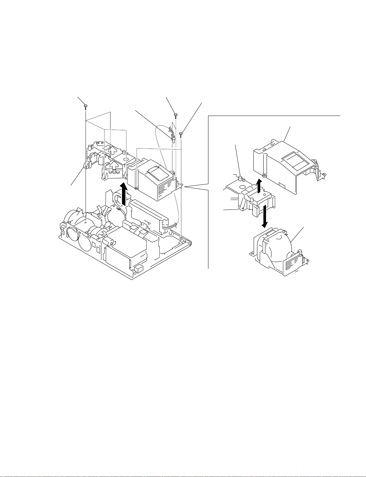
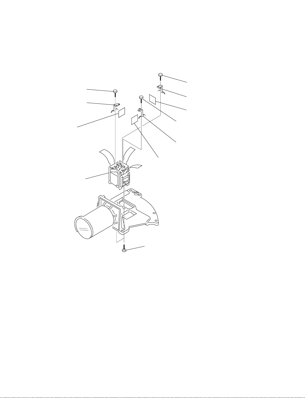
1-2-12.Lens Projection Assy and Lamp Duct Assy Removal
5 Lamp duct assy
3 Lens projection assy
1 Four screws
(+B 4 x 12)
2 Four screws
(+BSW M3 x 8)
4 T wo screws
(+B 3 x 6)
6 Screw
(+B 3 x 6)
7 Holder U
8 U board
To remove the lens projection assy and lamp duct assy , remove the C board, optics block assy and lamp assy
beforehand.
VPL-CS5/CX5
1-9
Page 18
1-2-13.Prism Block Assy and Out-pre-polarizer (R), (G), (B) Removal
n
Do not touch the flexible cable, glass surface of prism and especially the conductor surface of flexible cables.
2 Screw
(+PAP 2 x5)
3 Fastener (OP)
4 Out-pre-polarizer (R)
!- Prism block assy
8 Screw
(+PAP 2 x5)
9 Fastener (OP)
0 Out-pre-polarizer (G)
5 Screw
(+PAP 2 x5)
6 Fastener (OP)
7 Out-pre-polarizer (B)
1-10
1 T wo screws
(+PS 3 x 6)
VPL-CS5/CX5
Page 19
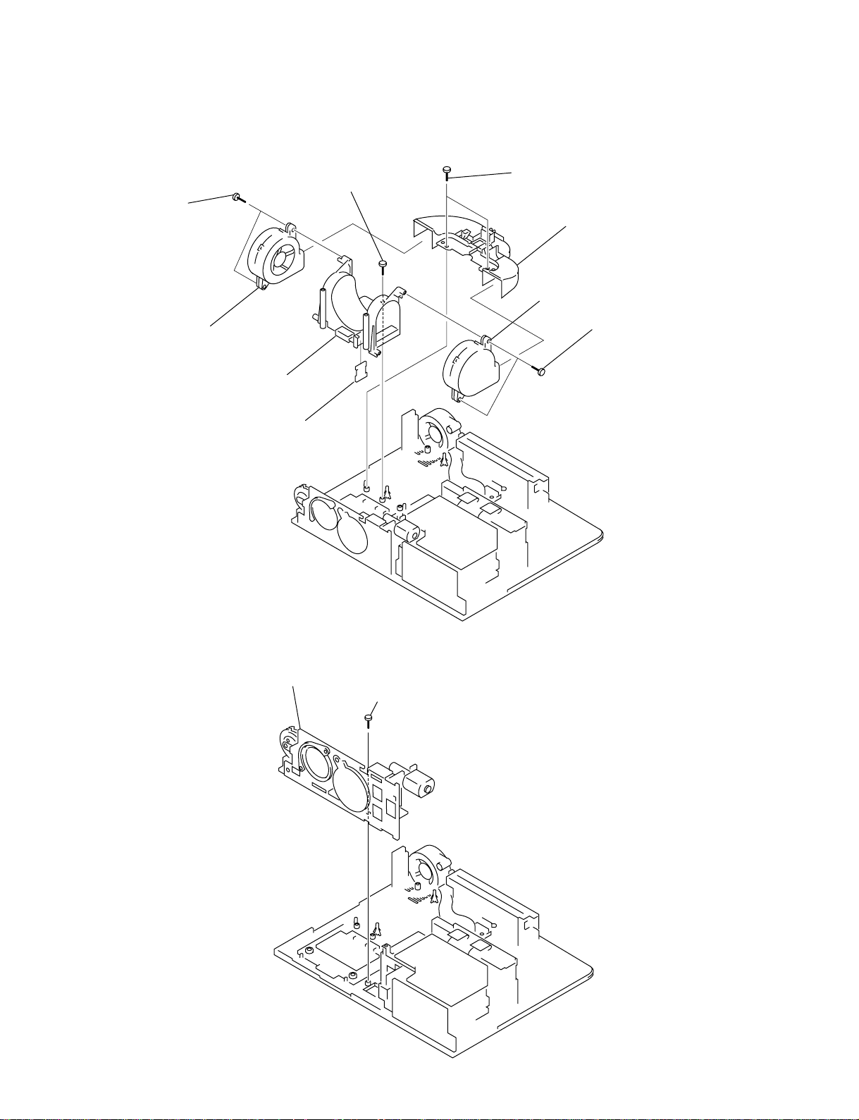
1-2-14.DC Fan (Sirocco) and V Board Removal
To remove the DC fan (sirocco) and V board, remove the C board, optics block assy, lamp assy
and prism block assy beforehand.
3 Screw (+B 3 x 6)
5 T wo screws
(+BTB 3 x 12)
1 T wo screws
(+B 3 x 6)
2 Prism duct
8 DC fan (sirocco)
6 DC fan (sirocco)
9 Fan holder (IN)
4 V board
1-2-15.Adjustor Unit Removal
To remove the adjustor unit, remove the C board, lamp assy, prism block assy and DC fan
(sirocco) beforehand.
2 Adjustor unit, Lens gear
7 T wo screws
(+BTB 3 x 12)
1 Screw (+B 3 x6)
VPL-CS5/CX5
1-11
Page 20
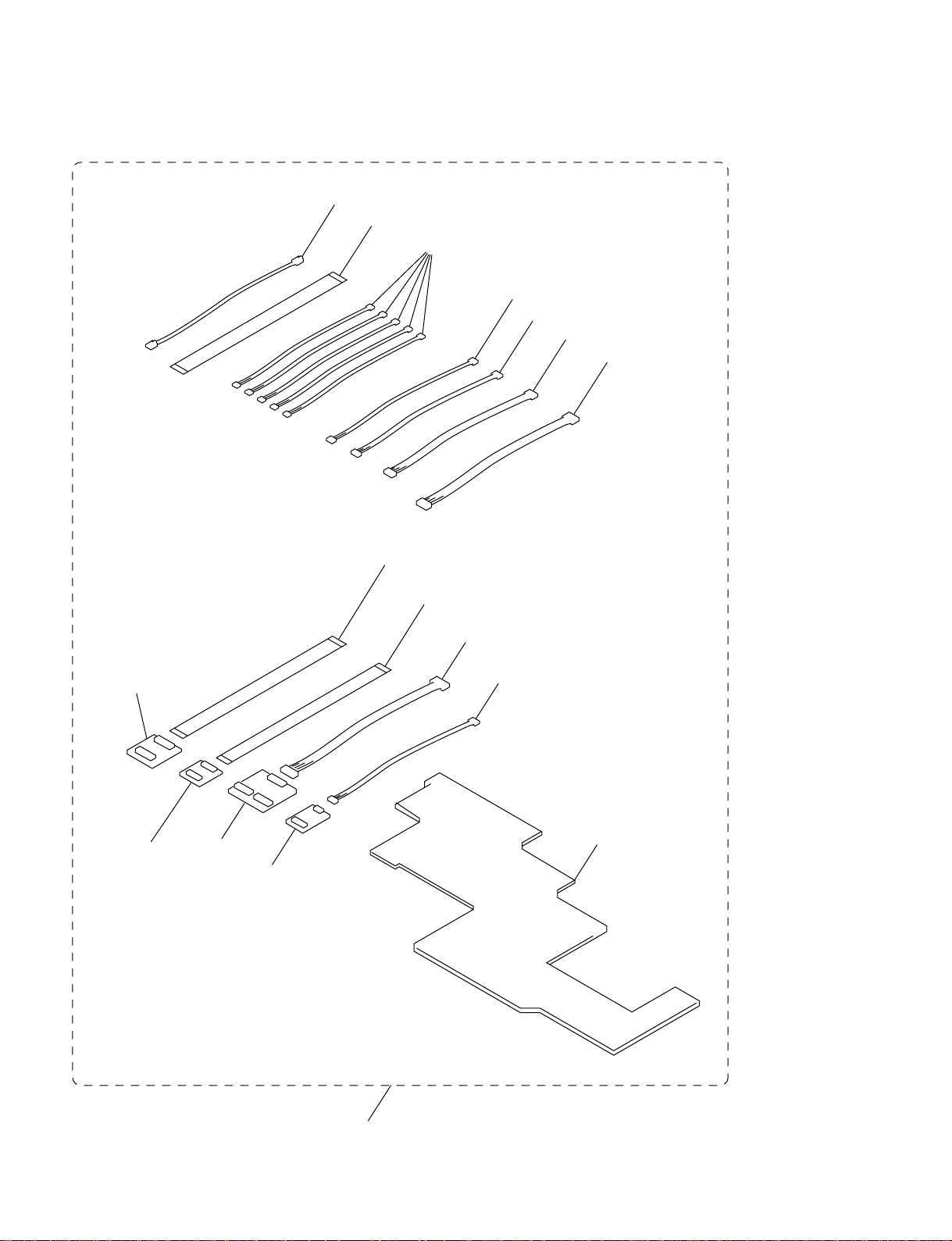
1-2-16.Extension Board and Extension Connectors
VH connector assy (3P)
Flat connector assy (24P)
Five ZH connectors assy (3P)
Three flat connectors assy (32P)
(VPL-CX5)
Three flat connectors assy (24P)
(VPL-CS5)
SR connector assy (4P)
ZH connector assy (5P)
SR connector assy (7P)
SR connector assy (14P)
Three X2 boards
(VPL-CX5)
Three X3 boards
(VPL-CS5)
X4 board
SR connector assy (12P)
SR connector assy (5P)
X1 board
X5 board
1-12
X kit assy
(A-1603-729-A)
VPL-CS5/CX5
Page 21
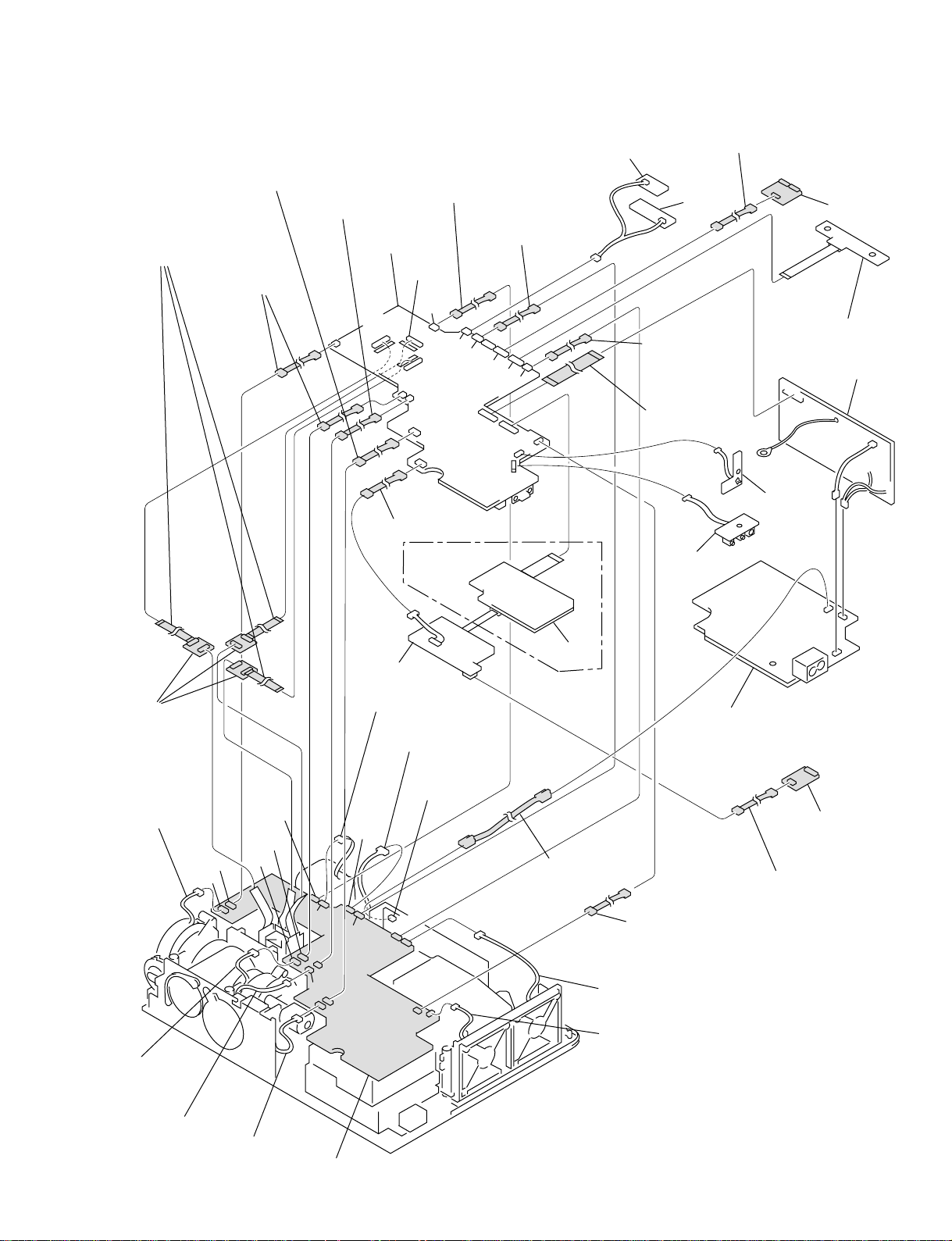
NR board
L board
C board
MS board
(VPL-CX5)
Two ZH connectors
assy (3P)
ZH connector assy (3P)
ZH connector assy
(3P)
ZH connector assy (5P)
ZH connector assy (3P)
ZH connector assy
(3P)
X5 board
(For VISCA)
(For writing the software)
SR connector assy (5P)
SR connector assy (12P)
X4 board
H1 board
CN909
CN907
CN914
CN912
CN910
CN110
CN112
CN111
CN911
CN101
CN901
CN911
CN701
*
CN702
CN601
*
CN602
CN501
*
CN502
CN901
CN904
CN1101
CN202
*
CN915
CN3301
CN108
CN3501
CN2001
CN2002
CN1302
CN1303
CN913
CN800
MSC board
Flat connector assy
(24P)
From DC fan
(Sirocco)
From DC fan
From DC fan
From DC fan
(Sirocco)
From V board
From adjustor unit
From DC fan
(Sirocco)
From power block
(Lamp), U board
Power block
(Lamp)
X board
GA board
GB board
CN301
CN1101
CN109
CN909
CN907
CN201
Q board
H2 board
CN903
CN908
CN908
CN910
CN1
SR connector assy (4P)
SR connector assy (7P)
SR connector assy (14P)
Three flat connectors assy
(32P) (VPL-CX5)
Three flat connectors assy
(24P) (VPL-CS5)
Three X2 boards
(VPL-CX5)
Three X3 boards
(VPL-CS5)
CN
912
CN107
1-2-17.Extension Board and Extension Connectors Connection
**
* : VPL-CX5
**
VPL-CS5/CX5
1-13
Page 22
1-2-18.Warning on Power Connection
Use the supplied power cord when you use the projector in your country.
Otherwise, use a proper power cord meeting the following specification.
The United Continental UK Australia Japan
States, Europe,
Canada Korrea
Plug type YP-11 YP-21 SP-61 B8 YP-13
Female end YC-13L YC-13L YC-13L C7-2 YC-13L
Cord type SPT-2 H03VVH2-F H03VVH2-F H03VVH2-F VFF
Rated Voltage & Current 10 A/125 V 2.5 A/250 V 2.5 A/250 V 2.5 A/250 V 7 A/125 V
Safety approval UL/CSA VDE BS SAA DENAN
Cord length (max.) 4.5 m ____
1-14
VPL-CS5/CX5
Page 23
Section 2
Electrical Adjustments
2-1. Preparation
2-1-1. Required Equipment
. Oscilloscope
Sony Tektronix 2465 or equivalent (350 MHz band
width or more)
. NTSC, PAL, SECAM component signal generator
Sony Tektronix TG2000 + AVG1 (option module) +
AWVG1 (option module) or equivalent
. VG (programmable video signal generator)
VG814 or equivalent
. Digital voltmeter
Advantest TR6845 or equivalent
. Illuminance meter
n
Allow the warm-up time of 5 minutes after the power is on
before starting the following adjustments.
2-1-2. Optical Unit Adjustment
9. Tighten the adjustment plate fixing screw.
10. Tighten the six adjustment plate fixing screws manually with a torque driver.
Tightening torque: 0.19 ±0.03 Nm
11. Check to see that the illumination range error is within
the tolerable limit.
When installing the optical unit in this model, alignment of
the gear tooth position is required. Perform the following
steps.
Lens
Lens gear
Gear alignment portion
Rotate the cooling fan and turn on the lamps.
(1) Mirror adjustment
Adjust the screen size to 80 inch at the WIDE end.
1. Select the green only mode.
2. Check to see if there is any black zone at the top,
bottom, left or right of screen. If there is any black
zone on screen, loosen the adjustment plate fixing
screw and adjust the G dichroic mirror for minimum
black zone.
3. Tighten the adjustment plate fixing screw.
4. Select the cyan only mode.
5. Check to see if there is any black zone at the top,
bottom, left or right of screen. If there is any black
zone on screen, loosen the adjustment plate fixing
screw and adjust the RB mirror adjustment plate for
minimum black zone and the blue color is distinguishing.
6. Tighten the adjustment plate fixing screw.
7. Select the all white mode.
8. Check to see if there is any black zone at the top,
bottom, left or right of screen. If there is any black
zone on screen, loosen the adjustment plate fixing
screw and adjust the RB mirror adjustment plate for
minimum black zone and the red color is distinguishing.
Procedure
1. Rotate the lens focus and zoom in the fully clockwise
positions. Lock the dial in the direction shown in Fig.
1.
Dial
Optical unit
Lens gear
Fig. 1
VPL-CS5/CX5
2-1
Page 24
2. Align the marking position of the optical unit gear
with the protrusion of the lens gear approximately by
visual observation as shown below.
Marking position
Optical unit
Lens gear
Protrusion
Fig. 2
Confirmation
When the optical unit is installed, rotate the gears upwards
and check to see engagement of the gears.
Teeth of the dial gear
are positioned higher
than the lens gear by
three teeth.
LensDial LensDial LensDial
Teeth of the dial gear
are positioned higher
than the lens gear by
two teeth.
Teeth of the dial gear
are positioned higher
than the lens gear by
one tooth.
2-1-3. How to Enter the Factory Mode
1. Confirm that the MENU can be displayed.
2. Close the MENU.
3. Press the keys in the following order : [ENTER] →
[ENTER] → [&] → [ENTER].
The message [Do you want to enter the Factory Mode?
Yes : ↑ No : ↓] appears.
Select [Yes : ↑].
[Supplementary information: How to Exit the
Factory Mode]
Perform the step 3 KEY operation.
The message [Do you want to return to the User Mode?
Yes : ↑ No : ↓] appears.
Select [Yes : ↑].
n
In the Factor mode, you can close the lens shutter if you
keep pressing the TILT key even though the lamp lights.
If the machine is left in this state for long hours, the lens
shutter may melt in the worst case. Be sure to confirm that
the lens shutter is not closed when the lamp lights in the
Factory mode.
Teeth of the lens gear
are positioned higher
than the dial gear by
one tooth.
LensDial LensDial
Teeth of the lens gear
are positioned higher
than the dial gear by
two teeth.
2-2. V COM Adjustment
1. Input the green-only, 30 IRE single-line ON/OFF
signal to the input connector.
(VPL-CS5 : SVGA signal, VPL-CX5 : XGA signal)
2. Enter the G VCOM adjustment screen of the Device
Adjust.
3. Adjust the G VCOM value so that the flicker is
minimal.
4. Switch the input signal from green-only to red-only
then to blue only single-line ON/OFF signal. In the
same way as step 3, adjust the R VCOM and B VCOM
values respectively so that the flicker is minimal.
5. Take note of the adjustment values.
6. Set the “Image Flip” to either V or HV.
7. Input the above R/G/B adjustment values.
8. Take note of the adjustment values.
9. Set the “Image Flip” to OFF.
2-2
VPL-CS5/CX5
Page 25
Picture Memory W/B Memory
StandardDynamic Standard Dynamic Standard High Low High Low
Dynamic
Standard
Video S Video Input-A MS Video Computer
Graphics Graphics Graphics
Graphics
Dynamic
Status Memory
Set Memory
Picture Mode Standard
Adjust Picture...
Contrast 95 80 95 80 95 80 95 80
Brightness 40 50 40 50 40 50 40 50
Color 50 50 50 50 50 50 __
Menu Title Item Name Memory Name Remark
2-3. Initial Values of Adjustment Items
VPL-CS5/CX5
PICTURE SETTING
__ __ 20 20 20 20
RGB Enhancer
Hue 50 50 50 50 __ __
Sharpness Middle Middle Middle Middle Middle Middle __
Gamma Mode __ __
Color Temp. Low Low Low Low High High High High
Volume 30
INPUT SETTING Adjust Signal...
Off
Computer
Dot Phase 15 (*)
H Size *
Shift *
Wide Mode Off Off Off Off Off Off Off Off
Scan Conv On On
Auto Input Search
Input-A Signal Sel.
Color System Auto
Power Saving Off
SET SETTING Smart APA On
MENU SETTING Status On
Languege English
Menu Position Center
Menu Color White
2-3
Page 26
Picture Memory W/B Memory
StandardDynamic Standard Dynamic Standard High Low High Low
Dynamic
Standard
Video S Video Input-A MS Video Computer
Dynamic
Status Memory
Set Memory
Display only
Display only
or each input signal (PRESET MEMORY No.).
2-4
Menu Title Item Name Memory Name Remark
Tilt...
V Keystone Auto
Manual... 0
Image Flip Off
INSTALL SETTING
Background Blue
Lamp Mode Low
INFORMATION fH Display only
fV Display only
(Memory No.) Display only
(Resolution) Display only
Lamp Timer Display only
ROM Version Display only
SC ROM Version
Operation Timer Display only
Prev. Lamp Timer
W/B SETTING Gain R 182 182 160 160
Gain G 182 150 160 140
Gain B 182 160 160 150
Bias R 85 85 85 85
Bias G 85 85 85 85
Bias B 85 85 85 85
* The “Dot Phase E, H Size, Shift H/V and Picture Mode” items in the “INPUT SETTING” menu have their respective initial values f
n
There are some adjustment items that cannot be adjusted, depending on the input signal.
VPL-CS5/CX5
Page 27
Fixed value
possible impossible
inversion is inversion is
Fixed value
Fixed value
Fixed value
Fixed value
Fixed value
Fixed value
.
.
Fixed value
Fixed value
Fixed value
Fixed value
Fixed value
Fixed value
Fixed value
Fixed value
Fixed value
Fixed value
Fixed value
Video S Video Input-A MS Up/Down Up/Down
Component
15kRGB
Chroma Memory Channel Memory Image Flip Memory
BW60 BW50
NT358/ Pal/Pal-M/
NT443/ N/Secam/ (15k)
Status Memory
8
20
32
Name Set Memory
Device Item Name Memory Name Remark
VPL-CS5/CX5
Clamp Width
R Gain 100
ADC/ Clamp Position
A/D
Converter
G Gain 100
B Gain 100
R Offset 128
G Offset 128
B Offset 128
Sync Sep Th
Pre Coast 2
Post Coast 8
Chroma/ Chroma/ Ch1 Gain 20 20 144 144
D.Comb Ch2 Gain 144 16 160 160
Video Brt 140 124 128 128
Video Cont 64 64 64 64
Sub Color 56 56 56 56
LCBW 00 00
Y-DeLay *
Ch3 Gain 144 144 160 160
Ch4 Gain 144 144 160 160
YUV Brt 128 128 128 128
YUV Cont 64 64 64 64
AOSL _
1E Display only
1F Display only
2-5
Page 28
Fixed value
Fixed value
Fixed value
Fixed value
Fixed value
Fixed value
Fixed value
Fixed value
Fixed value
Fixed value
Fixed value
Fixed value
Fixed value
possible impossible
inversion is inversion is
Video S Video Input-A MS Up/Down Up/Down
Component
15kRGB
Chroma Memory Channel Memory Image Flip Memory
55/65 55/65
55/65 55/65
55/65 55/65
Device Item Name Memory Name Remark
2-6
BW60 BW50
NT358/ Pal/Pal-M/
NT443/ N/Secam/ (15k)
Status Memory
Name Set Memory
Panel P.Drv Offset R 214 214
Driver Offset G 214 214
Offset B 214 214
V Common R
V Common G
V Common B
Psig 1 58/138
193
Psig 2 135/53
Signal Center
Gain R 166
Gain G 166
Gain B 166
Adj. not possible
DCFB Off 1
Sample SH1 7/8
Hold/
V Com Ptn Enb
Installation 0
Other/
R Osd Lvl 31
G Osd Lvl 31
B Osd Lvl 31
Through 0
SW 1
APC Thres 25
APC Limit 32
Gamma Sub Brt 0
Other 3D Sub Cont 0
VPL-CS5/CX5
Page 29
possible impossible
inversion is inversion is
Video S Video Input-A MS Up/Down Up/Down
Fixed value
Fixed value
Fixed value
Fixed value
Fixed value
Fixed value
Fixed value
Fixed value
Fixed value
Adj. not possible Adj. not possible
Fixed value
Fixed value
Fixed value
Adj. not possible Adj. not possible
Adj. not possible Adj. not possible
Adj. not possible Adj. not possible
Fixed value
Fixed value
Fixed value
Adj. not possible Adj. not possible
Adj. not possible Adj. not possible
Component
15kRGB
Chroma Memory Channel Memory Image Flip Memory
BW60 BW50
NT358/ Pal/Pal-M/
NT443/ N/Secam/ (15k)
Status Memory
104/144
0/1
H Start (MSB)
H Start (LSB)
H Position 33/11
9
HST Position
Adj. not possible
HST Phase 3/6
Temp Lamp
Adj. not possible
Temp Panel
Fan1 H
Fan1 L
Fan2 H
Fan2 L
Fan3 H
Fan3 L
1
Synchronous
Tilt C0 0
Tilt C1 10000
Tilt C2 _10000
X Tilt Display only
Y Tilt Display only
TL Display only
TP Display only
Factory
adjustment value
“7/8” the following meaning : Left digit : VPL-CS5, Right digit : VPL-CX5
Name Set Memory
Device Item Name Memory Name Remark
VPL-CS5/CX5
Other Other/ V Start 22
Gamma
m
.* : The value changes depending on the color systems and input terminals.
. There are some adjustment items that cannot be adjusted, depending on the input signal.
. The items showing two digits such as
2-7
Page 30

2-4. Service Know-How
2-5. White Balance Adjustment
2-4-1. When the Prism Block Is Replaced
1. Perform the V COM adjustment. (Refer to Section “2-
2. VCOM Adjustment”.)
2. Write the GAMMA data of the prism block.
3. Perform the white balance adjustment. (Refer to
Section “2-5. White Balance Adjustment”.)
2-4-2. When the C Board Is Replaced
n
If any board other than the C board is replaced, there is not
adjustment item.
1. Install IC406 of the C board before replacement, into
the new C board.
2. Enter the Factory Mode.
3. Place this model on a flat worktable. Press the TILT
key on a flat table so that the lens shutter becomes
visible a little when viewed from the front of the
model.
4. Operate the TILT+ key and stop it at the point that the
lens shutter becomes invisible from the front.
5. From this position, flip the TILT+ key twice.
6. Press the keys as follows [ENTER] → [ENTER] →
[POSITION+] → [MEMORY] keys. (Memorizing
the adjustment value.)
7. With the model being placed on a flat worktable, open
the lens shutter fully open while the adjuster does not
touch the ground.
8. Write the X TILT value in C0 at this time.
9. Point the model vertically upright and fix the position.
10. Write the X TILT value in C1 at this time.
11. Point the model vertically downward and fix the
position.
12. Write the X TILT value in C2 at this time.
13. Perform the V COM adjustment. (Refer to Section “2-
2. VCOM Adjustment”.)
14. If the white balance is significantly poor, perform the
white balance adjustment. . (Refer to Section “2-5.
White Balance Adjustment”.)
Preparation before adjustment
1. Input the 100 IRE flat field signal to the INPUT-A
connector and allow the warm-up of 10 minutes aging
at a minimum.
2. Enter the Service Mode.
Press the keys in the following order.
[ENTER] → [ENTER] → ↑ → ↓ → [ENTER].
The message [Do you want to enter the Service Mode?
Yes : ↑ No : ↓] appears.
Select [Yes : ↑].
[Supplementary information: How to Exit the
Service Mode]
Perform the step 2 KEY operation.
The message [Do you want to return to the User Mode?]
appears.
Select [Yes : ↑].
2-5-1. HIGH Mode of INPUT-A
Connect the10-step signal to the INPUT-A connector and
measure the chromaticities at each brightness.
If chromaticities are different at each brightness, perform
the following adjustment.
1. Input the 100 IRE flat field signal to the INPUT-A
connector.
2. Measure the chromaticity (x, y).
3. Input the 80 IRE flat field signal.
4. Adjust the GAIN R and GAIN B in the HIGH mode of
W/B until the chromaticity (x, y) that is measured at
step 2 is obtained.
5. Input the 30 IRE flat field signal.
6. Adjust the BIAS R and BIAS B in the HIGH mode of
W/B until the chromaticity (x, y) that is measured at
step 2 is obtained.
7. Repeat steps 3 to 6 until the chromaticity (x ±0.002, y
±0.004) with reference to the chromaticity (x, y) that
is measured at step 2 is obtained.
2-8
VPL-CS5/CX5
Page 31

2-5-2. LOW Mode of INPUT-A
2-5-4. LOW Mode of VIDEO
1. Input the 80 IRE flat field signal to the INPUT-A
connector.
2. In the LOW mode of W/B, adjust the GAIN R for +15
higher than the value in the HIGH mode, adjust the
GAIN G for
__
_25 lower than the value in the HIGH
__
mode and adjust GAIN B that is the same as the value
in the HIGH mode.
3. Adjust BIAS R, BIAS B and BIAS G for the same
value as those of the HIGH mode.
4. Measure the chromaticity (x, y).
5. Input the 30 IRE flat field signal.
6. Adjust the BIAS R and BIAS B in the LOW mode of
W/B until the chromaticity (x, y) that is measured at
step 4 is obtained.
7. Input the 80 IRE flat field signal.
8. Adjust the GAIN R and GAIN B in the LOW mode of
W/B until the chromaticity (x, y) that is measured at
step 4 is obtained.
9. Repeat steps 5 to 8 until the chromaticity (x ±0.002, y
±0.004) with reference to the chromaticity (x, y) that
is measured at step 4 is obtained.
1. Input the NTSC or PAL video signal to the input
connector.
2. In the LOW mode of W/B, adjust the GAIN R for
lower than the value in the INPUT-A LOW mode,
adjust the GAIN G for
__
_35 lower than the value in the
__
INPUT-A LOW mode and adjust GAIN B that is the
__
_20 lower than the value in the INPUT-A LOW mode.
__
3. Adjust BIAS G for
__
_5 lower than the value in the
__
INPUT-A LOW mode, adjust the BIAS R and BIAS B
for the same value as those of the INPUT-A HIGH
mode.
__
_20
__
2-5-3. HIGH Mode of VIDEO
1. Input the NTSC or PAL video signal to the input
connector.
2. In the HIGH mode of W/B, adjust the GAIN R for
__
_20 lower than the value in the INPUT-A HIGH
__
mode, adjust the GAIN G for
in the INPUT-A HIGH mode and adjust GAIN B that
__
is the
_20 lower than the value in the INPUT-A HIGH
__
mode.
3. Adjust BIAS G for
__
_5 lower than the value in the
__
INPUT-A HIGH mode, adjust the BIAS R and BIAS
B for the same value as those of the INPUT-A HIGH
mode.
__
_35 lower than the value
__
VPL-CS5/CX5
2-9
Page 32

2-6. Memory Structure
VPL-CS5 Series Memory Structure
CPU internal ROM : 384 K byte Flash Memory
CPU internal RAM : 24 K byte
External NVM memory : 8 K byte EEPROM
Set Memory Set MemorySet Memory
Status
Memory
Picture
Memory
Chroma
Memory
W/B
Memory
No.01
No.02
No.03
No.04
No.05
…
INPUT-A Preset
No.52
Video
S Video
Input-A
NT358/443/BW60
Component (15k)
Computer
Others
Dynamic
Standard
Dynamic
Standard
Dynamic
Standard
PAL/PAL-M/N/
SECAM/BW50
15k RGB
High
Low
High
Low
Status
Memory
Picture
Memory
Chroma
Memory
W/B
Memory
No.01
No.02
No.03
No.04
No.05
INPUT-
INPUT-
Video
S Video
Input-A
NT358/443/BW60
Component (15k)
Computer
Others
…
A Preset
No.52
No.101
…
A
User
No.120
Dynamic
Standard
Dynamic
Standard
Dynamic
Standard
PAL/PAL-M/N/
SECAM/BW50
15k RGB
High
Low
High
Low
Status Memory
Picture Memory
Chroma Memory
W/B
Memory
High
Low
Channel
Memory
Image Flip
Memory
2-10
Video
S Video
Input A
Up/Down inversion is impossible.
Up/Down inversion is possible.
CPU ROM
Initialize
Channel
Memory
Image Flip
Memory
Video
S Video
Input A
Up/Down inversion is impossible.
Up/Down inversion is possible.
External NVM
Channel Memory
Image Flip Memory
CPU RAM
Memory
Active memory copy
VPL-CS5/CX5
Page 33

Memory structure of VPL-CS5 consists of the followings.
1 Set memory
2 Status memory
3 Picture memory (picture quality mode memory)
4 Chroma memory
5 W/B memory
6 Channel memory
7 Image Flip memory
* The gamma memory is realized by giving offset to the Contrast and Brightness output values to the devices in the gamma mode
function.
Flow of data is described briefly. When the power plug is connected to the wall outlet for the first time
(Standby state), all data that are stored in the internal ROM are written in the NVM (non-volatile memory). When the POWER is turned ON, all the status memory data and other memory data that are required
for the present picture are selected from each memory block and expanded in the internal RAM.
When any adjustment is performed at this moment, the adjustment data (user mode items) are written in
the NVM (Service/Special Service items) automatically triggered by the memory operation.
The adjustment items (W/B, Device Adjust) that can be adjusted in the Service Mode or in the Special
Service Mode, are memorized in the NVM at the time when the user performs adjustment and performs
the memory operation. Note that the factory adjustment data will be lost at this moment.
VPL-CS5/CX5
2-11
Page 34

VPL-CX5 Series Memory Structure
CPU internal ROM : 384 K byte Flash Memory
CPU internal RAM : 24 K byte
External NVM memory : 8 K byte EEPROM
Set Memory Set MemorySet Memory
Status
Memory
Picture
Memory
INPUT-A Preset
MS Preset
Video
S Video
Input-A
MS
No.01
No.02
No.03
No.04
No.05
…
No.52
No.53
No.54
No.55
…
No.62
Dynamic
Standard
Dynamic
Standard
Dynamic
Standard
Dynamic
Standard
Status
Memory
Picture
Memory
INPUT-
A Preset
MS
Preset
A
User
INPUT-
Video
S Video
Input-A
MS
No.01
No.02
No.03
No.04
No.05
…
No.52
No.53
No.54
No.55
…
No.62
No.101
…
No.120
Dynamic
Standard
Dynamic
Standard
Dynamic
Standard
Dynamic
Standard
Status Memory
Picture Memory
Chroma
Memory
W/B
Memory
Channel
Memory
Image Flip
Memory
NT358/443/BW60
PAL/PAL-M/N/
SECAM/BW50
15k RGB
Component (15k)
Computer
Others
Up/Down inversion is impossible.
Up/Down inversion is possible.
CPU ROM
High
Low
High
Low
Video
S Video
Input A
MS
Initialize
Chroma
Memory
W/B
Memory
Channel
Memory
Image Flip
Memory
NT358/443/BW60
PAL/PAL-M/N/
SECAM/BW50
15k RGB
Component (15k)
Computer
Others
Video
S Video
Input A
MS
Up/Down inversion is impossible.
Up/Down inversion is possible.
External NVM
Chroma Memory
High
Low
High
Low
Active memory copy
W/B
Memory
Channel Memory
Image Flip Memory
Memory
High
Low
CPU RAM
2-12
VPL-CS5/CX5
Page 35

Memory structure of VPL-CX5 consists of the followings.
1 Set memory
2 Status memory
3 Picture memory (picture quality mode memory)
4 Chroma memory
5 W/B memory
6 Channel memory
7 Image Flip memory
* The gamma memory is realized by giving offset to the Contrast and Brightness output values to the devices in the gamma mode
function.
Flow of data is described briefly. When the power plug is connected to the wall outlet for the first time
(Standby state), all data that are stored in the internal ROM are written in the NVM (non-volatile memory). When the POWER is turned ON, all the status memory data and other memory data that are required
for the present picture are selected from each memory block and expanded in the internal RAM.
When any adjustment is performed at this moment, the adjustment data (user mode items) are written in
the NVM (Service/Special Service items) automatically triggered by the memory operation.
The adjustment items (W/B, Device Adjust) that can be adjusted in the Service Mode or in the Special
Service Mode, are memorized in the NVM at the time when the user performs adjustment and performs
the memory operation. Note that the factory adjustment data will be lost at this moment.
VPL-CS5/CX5
2-13
Page 36

Page 37

Section 3
Semiconductors
IC
24LC21AT/SN
BA033F-E2
BA033FP
BA033FP-E2
ICS332-SX1734
ICS332-SX1735
IRMF-A0T-QTP
M24C64-WMN6T(B)
MM1096AFF
SI9434DY-T1
ST24FC21M6TR
TA75W393FU
TA75W393FU-TE12R
TC7WH74FU(TE12R)
TL431BCDR2
1
TOP VIEW
8pin SOP
AD9883AKST-110
AD9883AKST-140
1
TOP VIEW
80pin QFP
BA05FP-E2
BA09FP-E2
VCC
GND
OUT
CXA3562AR-T6
UPD72012GB-003-3B4
1
TOP VIEW
100pin QFP
CXA7000R-T6
1
TOP VIEW
64pin QFP
LM1117MPX-1.8
ADJ/GND
OUTPUT
INPUT
LMC7101BIM5X
SN74AHC1G00DCKR
SN74AHCT1G04DCKR
SN74AHCT1G08DCKR
5
4
1
2
3
LP2985IM5X-3.3
5
4
1
3
LTC1772CS6
MB93401A
A
1
BOTTOM VIEW
288pin PGA
MB93491
1
TOP VIEW
176pin QFP
MBM29LV160BE-90TNMS1735
MBM29LV800TA-70PFTNSX1734
1
TOP VIEW
48pin SOP
MCZ3001D
ADXL202JE-REEL
1
2
8
3
7
6
4
5
INDEX
AK4352VT-E2
BA6288FS-E2
CY27027ZZCT
LT1765EFE
TPA2001D1PW
1
TOP VIEW
16pin SOP
CXD9607GB
A
1
BOTTOM VIEW
144pin PGA
HD64F2377VFQ33V
1
TOP VIEW
144pin QFP
L88M05T-FA-TL
1
3
1
TOP VIEW
6pin SOP
M52347FP-TE
SN74AHCT541PWR
SN74LV244APWR
TDA7309D013TR
1
TOP VIEW
20pin SOP
M62392FP
1
TOP VIEW
24pin SOP
1
TOP VIEW
40pin SOP
MT48LC8M16A2TG-75
MT48LC8M16A2TG-75TR
1
TOP VIEW
54pin SOP
MZ1540
1
3
2
5
4
7
9
8
10
VPL-CS5/CX5
3-1
Page 38

IC, T ransistor , Diode
PQ20VZ1U
1
2
3
4
5
PQ2TZ15U
1
5
PW164B-10TK
A
1
BOTTOM VIEW
256pin PGA
RCV4-A1T-MASK-25
ST72T631K4M1-201
1
TOP VIEW
34pin SOP
RS-140-T
4
1
3
2
S-80928ANMP-DDR-T2
S-80942ANMP-DD6-T2
1
2
3
SAA7118E/V1.518
SN74LV02APWR
SN74LV08APWR
SN74LV125APWR
SN74LVC125APWR-12
1
TOP VIEW
14pin SOP
SN74LV157APWR
1
TOP VIEW
18pin SOP
TC7S66FU
TC7S66FU(TE85R)
1
5pin CHIP
TC7SZ125FU(TE85R)
1
TOP VIEW
5pin SOP
TK11900MTL
1
6pin CHIP
2SA1162-G
2SA1162-YG-TE85L
2SA1576A-T106-QR
2SC2712-YG
2SC2712-YG-TE85L
2SC4081-R
2SC4081T106R
2SJ530S-TL
DTC144EUA-T106
C
2SA1213Y-TE12L
B
C
E
2SK2876-01MR-F122
GATE
DRAIN
SOURCE
DTA144EUA-T106
DTC114EU
OUT
IN
GND
HN1B01FU-TE85R
HN1C01FU-TE85R
6
5
1
2
1
6
3
2
5
3
HN1C03FU-TE85R
RN2904-TE85R
6
5
1
2
3
6
5
1
2
3
4
XP4501-TXE
4
5
6
3
2
1
4
5
3
2
1
6
1SS355TE-17
D2FS4-TA
EC31QS03L-TE12L
MA111-(K8).S0
MA111-TX
RD9.1SB2
RD9.1SB2-T1
ANODE
CATHODE
BZA456A
6
5
4
4
4
1
2
3
1
6
5
4
2
3
CL-190B1-X-T
4
KATHODE
ANODE
D10SC4M
D10SC6M
D10SC6M(RECTI)
A
1
BOTTOM VIEW
156pin PGA
3-2
B
E
1
2
3
1
2
3
VPL-CS5/CX5
Page 39

Diode
D2FS6-TA
CATHODE MARK
CATHODE
D6SB80
DAN202U
DAN202UT106
ANODE
ANODE
RB501V-40TE17
RB501V-40TE-17
ANODE
CATHODE
RD16M-B2
RD16M-T1B2
RD18M-B1
RD18M-T1B1
RD33M-B
RD33M-T1B
RD6.8M-B1
RD6.8M-T1B1
3
2
1
3
2
1
SEC1801C
SEC1901C
SEC2422C
CATHODE MARK
UDZSTE-173.9B
ANODE
CATHODE
CATHODE
NC
HN1D03FU-TE85L
HN1D03FU-TE85R
4
5
6
3
2
1
4
5
3
2
6
1
MA3J14700LSO
CATHODE
ANODE
NSCW100
KATHODE
RD3.9SB
RD3.9SB-T1
UF4005PKG23
CATHODE
ANODE
RM11C(RECTI)
RM11C-V1
CATHODE
ANODE
VPL-CS5/CX5
ANODE
3-3
Page 40

Page 41

4-1. Notes on Repair Parts
1. Safety Related Components Warning
w
Components marked ! are critical to safe operation.
Therefore, specified parts should be used in the case of
replacement.
[WARNHINWEIS][WARNHINWEIS]
[WARNHINWEIS]
[WARNHINWEIS][WARNHINWEIS]
Les composants identifiés par la marque ! sont
critiques pour la sécurité.
Ne les remplacer que par une pièce portant le numéro
spécifié.
2. Standardization of Parts
Some repair parts supplied by Sony differ from those
used for the unit. These are because of parts commonality and improvement.
Parts List has the present standardized repair parts.
Section 4
Spare Parts
3. Stock of Parts
Parts marked with “o” at SP (Supply Code) column of
the Spare Parts list may not be stocked. Therefore, the
delivery date will be delayed.
Items with no part number and no description are not
stocked because they are seldom required for routine
service.
4. Units for Capacitors, Inductors and Resistors
The following units are assumed in Schematic Diagrams, Electrical Parts List and Exploded Views
unless otherwise specified.
Capacitors : µF
Inductors : µH
Resistors : Ω
VPL-CS5/CX5
4-1
Page 42

Cover (VPL-CS5)
4-2. Exploded Views
16
8
9
3
5
13
2
+B 3x6
17
26
+B 3x6
+B 3x6
25
10
6
1
12
11
+B 3x20
21
+B 3x6
4
+B 3x6
22
26
23
15
+B 3x6
14
19
4-2
18
17
20
7
24
+B 3x6
VPL-CS5/CX5
Page 43

VPL-CS5 (Serial No. 10.001-) : (A1)
VPL-CS5 (Serial No. 5.000.001-) : (A2)
No. Part No. SP Description
1 A-1300-395-A s MOUNTED CIRCUIT BOARD, C (A1)
1 A-1300-487-A s MOUNTED CIRCUIT BOARD, C (A2)
2 A-1400-715-A s MOUNTED CIRCUIT BOARD, H1 (A1)
2 A-1400-916-A s MOUNTED CIRCUIT BOARD, H1 (A2)
3 A-1400-716-A s MOUNTED CIRCUIT BOARD, L (A1)
3 A-1400-917-A s MOUNTED CIRCUIT BOARD, L (A2)
4 A-1400-717-A s MOUNTED CIRCUIT BOARD, Q (A1)
4 A-1400-918-A s MOUNTED CIRCUIT BOARD, Q (A2)
5 A-1400-718-A s MOUNTED CIRCUIT BOARD, NR (A1)
5 A-1400-919-A s MOUNTED CIRCUIT BOARD, NR (A2)
6 A-1400-719-A s MOUNTED CIRCUIT BOARD, H2 (A1)
6 A-1400-920-A s MOUNTED CIRCUIT BOARD, H2 (A2)
7 X-4040-587-1 s LAMP COVER ASSY
8 X-4040-588-2 s BUTTON (H1) ASSY
9 X-4040-589-1 s PANEL ASSY, TOP
10 X-4040-590-1 s PANEL ASSY, SIDE
11 1-763-746-21 s FAN, DC
12 ! 1-900-222-47 s CONNECTOR ASSY A, FUSE 2P
13 1-900-268-34 s CONNECTOR ASSY A, FLAT 12P
14 4-074-246-02 o SLEEVE, VIDEO
Cover (VPL-CS5)
15 4-090-083-01 s MAGNET
16 4-090-085-01 s EMBLEM
17 4-090-087-01 s SHAFT
18 4-090-088-02 s FILTER
19 4-090-089-01 s FOOT, REAR
20 4-090-092-01 s FOOT, FRONT
21 4-090-095-01 s BUTTON (H2)
22 4-090-096-02 s LABEL, CONNECTOR NAME
23 4-090-099-02 s COVER, CONNECTOR
24 4-090-107-01 s COVER, FILTER
25 4-090-115-01 s HOLDER (H2)
26 4-090-741-01 s GASKET
Screws/Washers
7-682-547-04 s SCREW +B 3X6
7-682-553-09 s SCREW +B 3X20
VPL-CS5/CX5
4-3
Page 44

Cover (VPL-CX5)
24
8
9
3
5
13
2
+B 3x6
16
26
+B 3x6
+B 3x6
23
10
6
1
12
11
+B 3x20
20
+B 3x6
4
+B 3x6
25
26
21
15
+B 3x6
14
18
4-4
17
16
19
7
22
+B 3x6
VPL-CS5/CX5
Page 45

VPL-CX5 (Serial No. 10.001-) : (A3)
VPL-CX5 (Serial No. 5.000.001-) : (A4)
No. Part No. SP Description
1 A-1300-692-A s MOUNTED CIRCUIT BOARD, C (A3)
1 A-1300-747-A s MOUNTED CIRCUIT BOARD, C (A4)
2 A-1400-715-A s MOUNTED CIRCUIT BOARD, H1 (A3)
2 A-1400-916-A s MOUNTED CIRCUIT BOARD, H1 (A4)
3 A-1400-716-A s MOUNTED CIRCUIT BOARD, L (A3)
3 A-1400-917-A s MOUNTED CIRCUIT BOARD, L (A4)
4 A-1400-717-A s MOUNTED CIRCUIT BOARD, Q (A3)
4 A-1400-918-A s MOUNTED CIRCUIT BOARD, Q (A4)
5 A-1400-718-A s MOUNTED CIRCUIT BOARD, NR (A3)
5 A-1400-919-A s MOUNTED CIRCUIT BOARD, NR (A4)
6 A-1400-719-A s MOUNTED CIRCUIT BOARD, H2 (A3)
6 A-1400-920-A s MOUNTED CIRCUIT BOARD, H2 (A4)
7 X-4040-587-1 s LAMP COVER ASSY
8 X-4040-588-2 s BUTTON (H1) ASSY
9 X-4040-589-1 s PANEL ASSY, TOP
10 X-4040-590-1 s PANEL ASSY, SIDE
11 1-763-746-21 s FAN, DC
12 ! 1-900-222-47 s CONNECTOR ASSY A, FUSE 2P
13 1-900-268-34 s CONNECTOR ASSY A, FLAT 12P
14 4-074-246-02 o SLEEVE, VIDEO
Cover (VPL-CX5)
15 4-090-083-01 s MAGNET
16 4-090-087-01 s SHAFT
17 4-090-088-01 s FILTER
18 4-090-089-02 s FOOT, REAR
19 4-090-092-01 s FOOT, FRONT
20 4-090-095-01 s BUTTON (H2)
21 4-090-099-02 s COVER, CONNECTOR (A4)
21 4-090-099-11 s COVER, CONNECTOR (A3)
22 4-090-107-01 s COVER, FILTER
23 4-090-115-01 s HOLDER (H2)
24 4-090-337-01 s EMBLEM
25 4-090-339-01 s LABEL, CONNECTOR NAME
26 4-090-741-01 s GASKET
Screws/Washers
7-682-547-04 s SCREW +B 3X6
7-682-553-09 s SCREW +B 3X20
VPL-CS5/CX5
4-5
Page 46

Chassis (VPL-CS5)
106
+B 4x12
+B 4x12
103
+B 3x6
+B 3x6
105
102
+B 3x6
+B 3x6
101
+B 3x6
104
+PWHTP 3x10
4-6
VPL-CS5/CX5
Page 47

VPL-CS5 (Serial No. 10.001-) : (A1)
VPL-CS5 (Serial No. 5.000.001-) : (A2)
No. Part No. SP Description
101 A-1300-393-A s MOUNTED CIRCUIT BOARD, GA (A1)
101 A-1300-485-A s MOUNTED CIRCUIT BOARD, GA (A2)
102 A-1300-394-A s MOUNTED CIRCUIT BOARD, GB (A1)
102 A-1300-486-A s MOUNTED CIRCUIT BOARD, GB (A2)
103 A-1300-484-A s MOUNTED CIRCUIT BOARD, MSC (A2)
103 A-1300-663-A s MOUNTED CIRCUIT BOARD, MSC (A1)
104 A-1400-720-A s MOUNTED CIRCUIT BOARD, U (A1)
104 A-1400-914-A s MOUNTED CIRCUIT BOARD, U (A2)
105 1-900-267-27 s CONNECTOR ASSY, FLAT 24P
106 4-082-759-01 s SCREW, MACHINE, (+)P M4X12
Screws/Washers
7-682-547-04 s SCREW +B 3X6
7-682-563-04 s SCREW +B 4X12(EP-FE/CU,NI,CR)
7-685-903-31 s SCREW,+PWHTP 3X10(EP-FE/ZNBK/C)
Chassis (VPL-CS5)
VPL-CS5/CX5
4-7
Page 48

Chassis (VPL-CX5)
109
+B 4x12
+B 4x12
103
108
+B 3x6
+B 3x6
104
+B 3x6
106
107
+B 3x6
102
+B 3x6
101
+B 3x6
105
+PWHTP 3x10
4-8
VPL-CS5/CX5
Page 49

VPL-CX5 (Serial No. 10.001-) : (A3)
VPL-CX5 (Serial No. 5.000.001-) : (A4)
No. Part No. SP Description
101 A-1300-393-A s MOUNTED CIRCUIT BOARD, GA (A3)
101 A-1300-485-A s MOUNTED CIRCUIT BOARD, GA (A4)
102 A-1300-394-A s MOUNTED CIRCUIT BOARD, GB (A3)
102 A-1300-486-A s MOUNTED CIRCUIT BOARD, GB (A4)
103 A-1300-693-A s MOUNTED CIRCUIT BOARD, MS (A3)
103 A-1300-748-A s MOUNTED CIRCUIT BOARD, MS (A4)
104 A-1300-694-A s MOUNTED CIRCUIT BOARD, MSC (A3)
104 A-1300-749-A s MOUNTED CIRCUIT BOARD, MSC (A4)
105 A-1400-720-A s MOUNTED CIRCUIT BOARD, U (A3)
105 A-1400-914-A s MOUNTED CIRCUIT BOARD, U (A4)
106 1-900-267-27 s CONNECTOR ASSY, FLAT 24P
107 1-900-267-36 s CONNECTOR ASSY, FLAT 50P
108 1-900-267-37 s CONNECTOR ASSY B, FLAT 12P
109 4-082-759-01 s SCREW, MACHINE, (+)P M4X12
Screws/Washers
7-682-547-04 s SCREW +B 3X6
7-682-563-04 s SCREW +B 4X12(EP-FE/CU,NI,CR)
7-685-903-31 s SCREW,+PWHTP 3X10(EP-FE/ZNBK/C)
Chassis (VPL-CX5)
VPL-CS5/CX5
4-9
Page 50

Optics
201
202
205
+B 2x6
206
219
+B 2x6
+B 2x6
216
214
+B 2x6
203
208
+PTP 2x5
209
213
+PTP 2x5
+PTP 2x5
204
218
217
207
215
212
210
4-10
+PS 3x6
211
VPL-CS5/CX5
Page 51

VPL-CS5 (Serial No. 10.001-) : (A1)
VPL-CS5 (Serial No. 5.000.001-) : (A2)
VPL-CX5 (Serial No. 10.001-) : (A3)
VPL-CX5 (Serial No. 5.000.001-) : (A4)
No. Part No. SP Description
201 A-1603-660-A s OPT UNIT ASSY (A1)(A2)
201 A-1603-673-A s OPT UNIT ASSY (A3)(A4)
202 A-1603-661-A s PRISM BLOCK ASSY (A1)(A2)
202 A-1603-671-A s PRISM BLOCK ASSY (A3)(A4)
203 A-1603-662-A s PROJECTION LENS ASSY
204 A-1603-663-A s PS ASSY
205 A-1603-664-A s IN-POLARIZER (R) ASSY
206 A-1603-665-A s IN-POLARIZER (G) ASSY
207 A-1603-666-A s IN-POLARIZER (B) ASSY
208 A-1603-667-A s OUT-PRE-POLARIZER (R) ASSY
209 A-1603-668-A s OUT-PRE-POLARIZER (G) ASSY
210 A-1603-669-A s OUT-PRE-POLARIZER (B) ASSY
211 4-074-474-01 s +BSW M3X8
212 4-089-520-01 s APERTURE, PS COM
213 4-089-522-01 s FASTENER (OP)
214 4-089-526-01 s CUSHION
215 4-089-551-01 s PRE-FILTER, UV-CUT
216 4-089-552-01 s COVER (B), UNIT
Optics
217 4-089-558-01 s FLY EYE, LENS-1
218 4-089-559-01 s FLY EYE, LENS-2
219 4-090-112-01 o HOUSE, LAMP
Screws/Washers
7-621-772-38 s SCREW +B 2X6
7-682-647-09 s SCREW +PS 3X6(EP-FE/ZNBK/CM2)
7-685-103-19 s SCREW +PTP 2X5
VPL-CS5/CX5
4-11
Page 52

Base
+B 3x6
308
306
314
+BTB 3x12
+B 3x6
313
306
302
+BTB 3x12
+B 3x6
311
+B 3x6
+B 3x6
+B 3x6
306
+BTB 3x12
303
309
310
+B 3x6
+B 3x6
+BTB 3x12
307
305
301
+B 3x6
304
314
312
4-12
VPL-CS5/CX5
Page 53

VPL-CS5 (Serial No. 10.001-) : (A1)
VPL-CS5 (Serial No. 5.000.001-) : (A2)
VPL-CX5 (Serial No. 10.001-) : (A3)
VPL-CX5 (Serial No. 5.000.001-) : (A4)
No. Part No. SP Description
301 A-1400-721-A s MOUNTED CIRCUIT BOARD, V (A1)(A3)
301 A-1400-915-A s MOUNTED CIRCUIT BOARD, V (A2)(A4)
302 A-1603-156-A s SPEAKER ASSY (A1)(A3)
302 A-1603-250-A s SPEAKER ASSY (A2)(A4)
303 X-4040-721-1 o DUCT ASSY, LAMP
304 ! 1-468-696-11 s POWER BLOCK (LAMP)
305 1-477-433-11 s ADJUSTOR UNIT
306 1-763-886-11 s FAN, DC (SIROCCO)
307 4-090-090-01 s GEAR, LENS
308 4-090-104-01 o HOLDER, FAN (RE)
309 4-090-111-01 o DUCT, (LAMP)
310 4-090-114-01 s SHEET (LPS)
311 4-090-120-01 o HOLDER (IN), FAN
312 4-090-124-01 o BASE
313 4-090-740-01 s SHEET, DUCT
314 4-090-742-01 s SHEET (FAN)
Screws/Washers
Base
7-682-547-04 s SCREW +B3X6
7-685-548-19 s SCREW +BTB 3X12 (EP-FE/ZNBK/CM)
VPL-CS5/CX5
4-13
Page 54

VPL-CS5 (Serial No. 10.001-) : (A1) VPL-CX5 (Serial No. 10.001-) : (A3)
VPL-CS5 (Serial No. 5.000.001-) : (A2) VPL-CX5 (Serial No. 5.000.001-) : (A4)
4-3. Electrical Parts List
---------------C BOARD(VPL-CS5)
----------------
Note :
*1 If IC406 becomes defective, replace the entire C board.
(C BOARD)(VPL-CS5)
Ref. No.
or Q’ty Part No. SP Description
Ref. No.
or Q’ty Part No. SP Description
C155 1-164-947-11 s CAPACITOR CHIP CERAMIC 0.01MF
C156 1-107-820-11 s CAPACITOR,CHIP CERAMIC 0.1MF F
C157 1-107-820-11 s CAPACITOR,CHIP CERAMIC 0.1MF F
1pc A-1300-395-A s MOUNTED CIRCUIT BOARD, C(A1)
1pc A-1300-487-A s MOUNTED CIRCUIT BOARD, C(A2)
C100 1-164-947-11 s CAPACITOR CHIP CERAMIC 0.01MF
C101 1-164-947-11 s CAPACITOR CHIP CERAMIC 0.01MF
C102 1-164-947-11 s CAPACITOR CHIP CERAMIC 0.01MF
C103 1-126-205-11 s CAPACITOR,ELECT 47M/6.3
C104 1-126-205-11 s CAPACITOR,ELECT 47M/6.3
C105 1-115-566-11 s CAPACITOR,CERAMIC 4.7MF B/6.3V
C106 1-126-205-11 s CAPACITOR,ELECT 47M/6.3
C107 1-115-566-11 s CAPACITOR,CERAMIC 4.7MF B/6.3V
C108 1-107-820-11 s CAPACITOR,CHIP CERAMIC 0.1MF F
C109 1-107-820-11 s CAPACITOR,CHIP CERAMIC 0.1MF F
C111 1-107-820-11 s CAPACITOR,CHIP CERAMIC 0.1MF F
C112 1-107-820-11 s CAPACITOR,CHIP CERAMIC 0.1MF F
C113 1-107-820-11 s CAPACITOR,CHIP CERAMIC 0.1MF F
C114 1-164-937-11 s CAPACITOR,CHIP CERAMIC 1000PF
C115 1-109-982-11 s CAPACITOR,CHIP CERAMIC 1MF/10V
C116 1-107-820-11 s CAPACITOR,CHIP CERAMIC 0.1MF F
C117 1-137-987-81 s CAPACITOR,C.CERAMIC 0.068MF
C118 1-115-566-11 s CAPACITOR,CERAMIC 4.7MF B/6.3V
C119 1-115-566-11 s CAPACITOR,CERAMIC 4.7MF B/6.3V
C120 1-165-875-11 s CAPACITOR,CHIP CERAMIC 10MF B
C121 1-165-871-11 s CAPACITOR,ELECT 22MF
C122 1-107-820-11 s CAPACITOR,CHIP CERAMIC 0.1MF F
C123 1-165-875-11 s CAPACITOR,CHIP CERAMIC 10MF B
C124 1-107-820-11 s CAPACITOR,CHIP CERAMIC 0.1MF F
C125 1-164-947-11 s CAPACITOR CHIP CERAMIC 0.01MF
C158 1-164-947-11 s CAPACITOR CHIP CERAMIC 0.01MF
C159 1-164-947-11 s CAPACITOR CHIP CERAMIC 0.01MF
C160 1-107-820-11 s CAPACITOR,CHIP CERAMIC 0.1MF F
C161 1-164-505-11 s CAPACITOR,CHIP CERAMIC 2.2MF
C162 1-107-820-11 s CAPACITOR,CHIP CERAMIC 0.1MF F
C163 1-164-874-11 s CAPACITOR,CHIP CERAMIC 100PF
C164 1-107-820-11 s CAPACITOR,CHIP CERAMIC 0.1MF F
C165 1-107-820-11 s CAPACITOR,CHIP CERAMIC 0.1MF F
C166 1-107-820-11 s CAPACITOR,CHIP CERAMIC 0.1MF F
C200 1-164-854-11 s CAPACITOR CERAMIC 15PF/16V CH
C201 1-164-854-11 s CAPACITOR CERAMIC 15PF/16V CH
C206 1-127-772-11 s CAPACTOR C,CERAMIC 33000PF B
C207 1-119-923-11 s CAPACITOR,CHIP CERAMIC 0.047MF
C208 1-119-923-11 s CAPACITOR,CHIP CERAMIC 0.047MF
C209 1-127-772-11 s CAPACTOR C,CERAMIC 33000PF B
C210 1-119-923-11 s CAPACITOR,CHIP CERAMIC 0.047MF
C211 1-127-772-11 s CAPACTOR C,CERAMIC 33000PF B
C215 1-127-772-11 s CAPACTOR C,CERAMIC 33000PF B
C216 1-127-772-11 s CAPACTOR C,CERAMIC 33000PF B
C217 1-127-772-11 s CAPACTOR C,CERAMIC 33000PF B
C218 1-127-772-11 s CAPACTOR C,CERAMIC 33000PF B
C219 1-119-923-11 s CAPACITOR,CHIP CERAMIC 0.047MF
C220 1-126-206-11 s CAPACITOR, ELECT 100MF/6.3V
C221 1-165-871-11 s CAPACITOR,ELECT 22MF
C222 1-107-820-11 s CAPACITOR,CHIP CERAMIC 0.1MF F
C223 1-107-820-11 s CAPACITOR,CHIP CERAMIC 0.1MF F
C224 1-107-820-11 s CAPACITOR,CHIP CERAMIC 0.1MF F
C126 1-164-882-11 s CAPACITOR,CERAMIC 220PF/16V CH
C127 1-164-874-11 s CAPACITOR,CHIP CERAMIC 100PF
C128 1-125-837-11 s CAPACITOR,CHIP CERAMIC1MF/6.3V
C129 1-165-871-21 s CAPACITOR,SOLID ELECT 22MF
C130 1-107-820-11 s CAPACITOR,CHIP CERAMIC 0.1MF F
C131 1-119-923-11 s CAPACITOR,CHIP CERAMIC 0.047MF
C132 1-119-923-11 s CAPACITOR,CHIP CERAMIC 0.047MF
C133 1-164-937-11 s CAPACITOR,CHIP CERAMIC 1000PF
C134 1-119-923-11 s CAPACITOR,CHIP CERAMIC 0.047MF
C135 1-107-820-11 s CAPACITOR,CHIP CERAMIC 0.1MF F
C136 1-131-998-11 s CAP, SOLID ELECT 82MF 6.3 V
C137 1-164-947-11 s CAPACITOR CHIP CERAMIC 0.01MF
C138 1-119-667-11 s CAPACITOR CERAMIC 22MF/10V(F)
C139 1-107-820-11 s CAPACITOR,CHIP CERAMIC 0.1MF F
C140 1-107-820-11 s CAPACITOR,CHIP CERAMIC 0.1MF F
C141 1-107-820-11 s CAPACITOR,CHIP CERAMIC 0.1MF F
C142 1-107-820-11 s CAPACITOR,CHIP CERAMIC 0.1MF F
C143 1-164-947-11 s CAPACITOR CHIP CERAMIC 0.01MF
C144 1-164-947-11 s CAPACITOR CHIP CERAMIC 0.01MF
C145 1-107-820-11 s CAPACITOR,CHIP CERAMIC 0.1MF F
C146 1-107-820-11 s CAPACITOR,CHIP CERAMIC 0.1MF F
C147 1-164-947-11 s CAPACITOR CHIP CERAMIC 0.01MF
C148 1-107-820-11 s CAPACITOR,CHIP CERAMIC 0.1MF F
C149 1-164-947-11 s CAPACITOR CHIP CERAMIC 0.01MF
C150 1-107-820-11 s CAPACITOR,CHIP CERAMIC 0.1MF F
C151 1-164-173-11 s CAPACITOR,CERAMIC 3900PF/50V B
C152 1-137-652-91 s CAPACITOR,CERAMIC 39000PF /16V
C153 1-107-820-11 s CAPACITOR,CHIP CERAMIC 0.1MF F
C154 1-107-820-11 s CAPACITOR,CHIP CERAMIC 0.1MF F
C225 1-107-820-11 s CAPACITOR,CHIP CERAMIC 0.1MF F
C226 1-164-943-11 s CAPACITOR,CHIP CERAMIC 0.01MF
C227 1-164-943-11 s CAPACITOR,CHIP CERAMIC 0.01MF
C228 1-164-943-11 s CAPACITOR,CHIP CERAMIC 0.01MF
C229 1-164-943-11 s CAPACITOR,CHIP CERAMIC 0.01MF
C230 1-107-820-11 s CAPACITOR,CHIP CERAMIC 0.1MF F
C233 1-107-820-11 s CAPACITOR,CHIP CERAMIC 0.1MF F
C234 1-165-871-11 s CAPACITOR,ELECT 22MF
C245 1-107-820-11 s CAPACITOR,CHIP CERAMIC 0.1MF F
C260 1-107-820-11 s CAPACITOR,CHIP CERAMIC 0.1MF F
C261 1-107-820-11 s CAPACITOR,CHIP CERAMIC 0.1MF F
C262 1-164-947-11 s CAPACITOR CHIP CERAMIC 0.01MF
C263 1-119-667-11 s CAPACITOR CERAMIC 22MF/10V(F)
C300 1-107-820-11 s CAPACITOR,CHIP CERAMIC 0.1MF F
C301 1-119-667-11 s CAPACITOR CERAMIC 22MF/10V(F)
C302 1-107-820-11 s CAPACITOR,CHIP CERAMIC 0.1MF F
C303 1-107-820-11 s CAPACITOR,CHIP CERAMIC 0.1MF F
C304 1-107-820-11 s CAPACITOR,CHIP CERAMIC 0.1MF F
C305 1-107-820-11 s CAPACITOR,CHIP CERAMIC 0.1MF F
C306 1-107-820-11 s CAPACITOR,CHIP CERAMIC 0.1MF F
C307 1-107-820-11 s CAPACITOR,CHIP CERAMIC 0.1MF F
C308 1-107-820-11 s CAPACITOR,CHIP CERAMIC 0.1MF F
C309 1-107-820-11 s CAPACITOR,CHIP CERAMIC 0.1MF F
C310 1-107-820-11 s CAPACITOR,CHIP CERAMIC 0.1MF F
C311 1-107-820-11 s CAPACITOR,CHIP CERAMIC 0.1MF F
C312 1-107-820-11 s CAPACITOR,CHIP CERAMIC 0.1MF F
C314 1-107-820-11 s CAPACITOR,CHIP CERAMIC 0.1MF F
C315 1-107-820-11 s CAPACITOR,CHIP CERAMIC 0.1MF F
C316 1-164-852-11 s CAPACITOR,CHIP CERAMIC 12PF/16
4-14
VPL-CS5/CX5
Page 55

(C BOARD)(VPL-CS5)
(C BOARD)(VPL-CS5)
Ref. No.
or Q’ty Part No. SP Description
C317 1-107-820-11 s CAPACITOR,CHIP CERAMIC 0.1MF F
C318 1-107-820-11 s CAPACITOR,CHIP CERAMIC 0.1MF F
C319 1-164-852-11 s CAPACITOR,CHIP CERAMIC 12PF/16
C320 1-107-820-11 s CAPACITOR,CHIP CERAMIC 0.1MF F
C321 1-164-947-11 s CAPACITOR CHIP CERAMIC 0.01MF
C322 1-107-820-11 s CAPACITOR,CHIP CERAMIC 0.1MF F
C323 1-107-820-11 s CAPACITOR,CHIP CERAMIC 0.1MF F
C324 1-107-820-11 s CAPACITOR,CHIP CERAMIC 0.1MF F
C325 1-107-820-11 s CAPACITOR,CHIP CERAMIC 0.1MF F
C328 1-164-947-11 s CAPACITOR CHIP CERAMIC 0.01MF
C329 1-107-820-11 s CAPACITOR,CHIP CERAMIC 0.1MF F
C330 1-119-667-11 s CAPACITOR CERAMIC 22MF/10V(F)
C331 1-107-820-11 s CAPACITOR,CHIP CERAMIC 0.1MF F
C332 1-107-820-11 s CAPACITOR,CHIP CERAMIC 0.1MF F
C333 1-107-820-11 s CAPACITOR,CHIP CERAMIC 0.1MF F
C334 1-107-820-11 s CAPACITOR,CHIP CERAMIC 0.1MF F
C335 1-107-820-11 s CAPACITOR,CHIP CERAMIC 0.1MF F
C336 1-107-820-11 s CAPACITOR,CHIP CERAMIC 0.1MF F
C337 1-107-820-11 s CAPACITOR,CHIP CERAMIC 0.1MF F
C338 1-107-820-11 s CAPACITOR,CHIP CERAMIC 0.1MF F
C339 1-107-820-11 s CAPACITOR,CHIP CERAMIC 0.1MF F
C340 1-107-820-11 s CAPACITOR,CHIP CERAMIC 0.1MF F
C341 1-107-820-11 s CAPACITOR,CHIP CERAMIC 0.1MF F
C342 1-107-820-11 s CAPACITOR,CHIP CERAMIC 0.1MF F
C401 1-107-820-11 s CAPACITOR,CHIP CERAMIC 0.1MF F
Ref. No.
or Q’ty Part No. SP Description
C513 1-128-992-11 s CAPACITOR ELECT 47MF 25V
C514 1-128-992-11 s CAPACITOR ELECT 47MF 25V
C515 1-164-156-11 s CAPACITOR,CERAMIC 0.1MF/25V F
C516 1-164-156-11 s CAPACITOR,CERAMIC 0.1MF/25V F
C517 1-164-156-11 s CAPACITOR,CERAMIC 0.1MF/25V F
C518 1-164-156-11 s CAPACITOR,CERAMIC 0.1MF/25V F
C519 1-164-156-11 s CAPACITOR,CERAMIC 0.1MF/25V F
C520 1-117-681-11 s CAPACITOR, ELECT 100MF/16V
C521 1-164-156-11 s CAPACITOR,CERAMIC 0.1MF/25V F
C550 1-164-947-11 s CAPACITOR CHIP CERAMIC 0.01MF
C552 1-115-340-11 s CAPACITOR CERAMIC 0.22MF/25V B
C553 1-164-156-11 s CAPACITOR,CERAMIC 0.1MF/25V F
C554 1-164-156-11 s CAPACITOR,CERAMIC 0.1MF/25V F
C555 1-128-992-11 s CAPACITOR ELECT 47MF 25V
C601 1-107-820-11 s CAPACITOR,CHIP CERAMIC 0.1MF F
C602 1-127-715-11 s CAPACITOR,CERAMIC 0.22MF B1608
C603 1-107-820-11 s CAPACITOR,CHIP CERAMIC 0.1MF F
C604 1-126-206-11 s CAPACITOR, ELECT 100MF/6.3V
C605 1-127-715-11 s CAPACITOR,CERAMIC 0.22MF B1608
C606 1-127-715-11 s CAPACITOR,CERAMIC 0.22MF B1608
C607 1-127-715-11 s CAPACITOR,CERAMIC 0.22MF B1608
C608 1-127-715-11 s CAPACITOR,CERAMIC 0.22MF B1608
C609 1-127-715-11 s CAPACITOR,CERAMIC 0.22MF B1608
C610 1-127-715-11 s CAPACITOR,CERAMIC 0.22MF B1608
C611 1-127-715-11 s CAPACITOR,CERAMIC 0.22MF B1608
C402 1-107-820-11 s CAPACITOR,CHIP CERAMIC 0.1MF F
C403 1-164-874-11 s CAPACITOR,CHIP CERAMIC 100PF
C404 1-107-820-11 s CAPACITOR,CHIP CERAMIC 0.1MF F
C406 1-107-820-11 s CAPACITOR,CHIP CERAMIC 0.1MF F
C407 1-107-820-11 s CAPACITOR,CHIP CERAMIC 0.1MF F
C408 1-107-820-11 s CAPACITOR,CHIP CERAMIC 0.1MF F
C409 1-107-820-11 s CAPACITOR,CHIP CERAMIC 0.1MF F
C410 1-107-820-11 s CAPACITOR,CHIP CERAMIC 0.1MF F
C411 1-107-820-11 s CAPACITOR,CHIP CERAMIC 0.1MF F
C412 1-107-820-11 s CAPACITOR,CHIP CERAMIC 0.1MF F
C413 1-107-820-11 s CAPACITOR,CHIP CERAMIC 0.1MF F
C414 1-107-820-11 s CAPACITOR,CHIP CERAMIC 0.1MF F
C415 1-126-205-11 s CAPACITOR,ELECT 47M/6.3
C416 1-164-947-11 s CAPACITOR CHIP CERAMIC 0.01MF
C450 1-107-820-11 s CAPACITOR,CHIP CERAMIC 0.1MF F
C451 1-107-820-11 s CAPACITOR,CHIP CERAMIC 0.1MF F
C452 1-107-820-11 s CAPACITOR,CHIP CERAMIC 0.1MF F
C471 1-107-820-11 s CAPACITOR,CHIP CERAMIC 0.1MF F
C472 1-126-205-11 s CAPACITOR,ELECT 47M/6.3
C473 1-107-820-11 s CAPACITOR,CHIP CERAMIC 0.1MF F
C474 1-164-935-11 s CAPACITOR,CHIP CERAMIC 470PF
C475 1-164-935-11 s CAPACITOR,CHIP CERAMIC 470PF
C501 1-107-820-11 s CAPACITOR,CHIP CERAMIC 0.1MF F
C502 1-127-715-11 s CAPACITOR,CERAMIC 0.22MF B1608
C503 1-107-820-11 s CAPACITOR,CHIP CERAMIC 0.1MF F
C504 1-126-206-11 s CAPACITOR, ELECT 100MF/6.3V
C505 1-127-715-11 s CAPACITOR,CERAMIC 0.22MF B1608
C506 1-127-715-11 s CAPACITOR,CERAMIC 0.22MF B1608
C507 1-127-715-11 s CAPACITOR,CERAMIC 0.22MF B1608
C508 1-127-715-11 s CAPACITOR,CERAMIC 0.22MF B1608
C612 1-164-156-11 s CAPACITOR,CERAMIC 0.1MF/25V F
C613 1-128-992-11 s CAPACITOR ELECT 47MF 25V
C614 1-128-992-11 s CAPACITOR ELECT 47MF 25V
C615 1-164-156-11 s CAPACITOR,CERAMIC 0.1MF/25V F
C616 1-164-156-11 s CAPACITOR,CERAMIC 0.1MF/25V F
C617 1-164-156-11 s CAPACITOR,CERAMIC 0.1MF/25V F
C618 1-164-156-11 s CAPACITOR,CERAMIC 0.1MF/25V F
C619 1-164-156-11 s CAPACITOR,CERAMIC 0.1MF/25V F
C620 1-117-681-11 s CAPACITOR, ELECT 100MF/16V
C621 1-164-156-11 s CAPACITOR,CERAMIC 0.1MF/25V F
C701 1-107-820-11 s CAPACITOR,CHIP CERAMIC 0.1MF F
C702 1-127-715-11 s CAPACITOR,CERAMIC 0.22MF B1608
C703 1-107-820-11 s CAPACITOR,CHIP CERAMIC 0.1MF F
C704 1-126-206-11 s CAPACITOR, ELECT 100MF/6.3V
C705 1-127-715-11 s CAPACITOR,CERAMIC 0.22MF B1608
C706 1-127-715-11 s CAPACITOR,CERAMIC 0.22MF B1608
C707 1-127-715-11 s CAPACITOR,CERAMIC 0.22MF B1608
C708 1-127-715-11 s CAPACITOR,CERAMIC 0.22MF B1608
C709 1-127-715-11 s CAPACITOR,CERAMIC 0.22MF B1608
C710 1-127-715-11 s CAPACITOR,CERAMIC 0.22MF B1608
C711 1-127-715-11 s CAPACITOR,CERAMIC 0.22MF B1608
C712 1-164-156-11 s CAPACITOR,CERAMIC 0.1MF/25V F
C713 1-128-992-11 s CAPACITOR ELECT 47MF 25V
C714 1-128-992-11 s CAPACITOR ELECT 47MF 25V
C715 1-164-156-11 s CAPACITOR,CERAMIC 0.1MF/25V F
C716 1-164-156-11 s CAPACITOR,CERAMIC 0.1MF/25V F
C717 1-164-156-11 s CAPACITOR,CERAMIC 0.1MF/25V F
C718 1-164-156-11 s CAPACITOR,CERAMIC 0.1MF/25V F
C719 1-164-156-11 s CAPACITOR,CERAMIC 0.1MF/25V F
C720 1-117-681-11 s CAPACITOR, ELECT 100MF/16V
C509 1-127-715-11 s CAPACITOR,CERAMIC 0.22MF B1608
C510 1-127-715-11 s CAPACITOR,CERAMIC 0.22MF B1608
C511 1-127-715-11 s CAPACITOR,CERAMIC 0.22MF B1608
C512 1-164-156-11 s CAPACITOR,CERAMIC 0.1MF/25V F
VPL-CS5/CX5
C721 1-164-156-11 s CAPACITOR,CERAMIC 0.1MF/25V F
C800 1-124-778-00 s CAPACITOR,ELECT 22MF/6.3V
C801 1-164-947-11 s CAPACITOR CHIP CERAMIC 0.01MF
C802 1-165-871-11 s CAPACITOR,ELECT 22MF
4-15
Page 56

(C BOARD)(VPL-CS5)
(C BOARD)(VPL-CS5)
Ref. No.
or Q’ty Part No. SP Description
C803 1-115-566-11 s CAPACITOR,CERAMIC 4.7MF B/6.3V
C804 1-107-820-11 s CAPACITOR,CHIP CERAMIC 0.1MF F
C805 1-164-947-11 s CAPACITOR CHIP CERAMIC 0.01MF
C806 1-107-820-11 s CAPACITOR,CHIP CERAMIC 0.1MF F
C807 1-164-852-11 s CAPACITOR,CHIP CERAMIC 12PF/16
C808 1-107-820-11 s CAPACITOR,CHIP CERAMIC 0.1MF F
C809 1-164-852-11 s CAPACITOR,CHIP CERAMIC 12PF/16
C810 1-164-947-11 s CAPACITOR CHIP CERAMIC 0.01MF
C811 1-107-820-11 s CAPACITOR,CHIP CERAMIC 0.1MF F
Ref. No.
or Q’ty Part No. SP Description
C1127 1-115-156-11 s CAPACITOR,CERAMIC 1MF/10V(1608
C1128 1-115-156-11 s CAPACITOR,CERAMIC 1MF/10V(1608
C1137 1-117-681-11 s CAPACITOR, ELECT 100MF/16V
C1138 1-125-777-11 s CAPACITOR CERAMIC 0.1MF/10V
C1140 1-107-820-11 s CAPACITOR,CHIP CERAMIC 0.1MF F
C1143 1-107-820-11 s CAPACITOR,CHIP CERAMIC 0.1MF F
C1144 1-125-777-11 s CAPACITOR CERAMIC 0.1MF/10V
C1145 1-125-777-11 s CAPACITOR CERAMIC 0.1MF/10V
C1146 1-125-777-11 s CAPACITOR CERAMIC 0.1MF/10V
C812 1-107-820-11 s CAPACITOR,CHIP CERAMIC 0.1MF F
CN100 1-784-828-11 s CONNECTOR, D SUB
C813 1-107-820-11 s CAPACITOR,CHIP CERAMIC 0.1MF F
C814 1-115-156-11 s CAPACITOR,CERAMIC 1MF/10V(1608
C815 1-107-820-11 s CAPACITOR,CHIP CERAMIC 0.1MF F
C816 1-107-820-11 s CAPACITOR,CHIP CERAMIC 0.1MF F
CN201 1-770-629-21 s PIN, CONNECTOR 12P
CN401 1-770-621-21 s PIN, CONNECTOR 4P
CN502 1-779-730-11 s CONNECTOR, FFC/FPC (ZIF) 24P
CN602 1-779-730-11 s CONNECTOR, FFC/FPC (ZIF) 24P
C817 1-124-778-00 s CAPACITOR,ELECT 22MF/6.3V
CN702 1-779-730-11 s CONNECTOR, FFC/FPC (ZIF) 24P
C818 1-164-940-11 s CAPACITOR,CHIP CERAMIC 3300/16
C819 1-107-820-11 s CAPACITOR,CHIP CERAMIC 0.1MF F
C820 1-107-820-11 s CAPACITOR,CHIP CERAMIC 0.1MF F
C821 1-107-820-11 s CAPACITOR,CHIP CERAMIC 0.1MF F
CN800 1-770-629-21 s PIN, CONNECTOR 12P
CN901 1-770-621-21 s PIN, CONNECTOR 4P
CN903 1-691-491-21 s CONNECTOR, FFC/FPC 12P
CN904 1-764-829-11 o CONNECTOR, FPC 24P
C822 1-164-940-11 s CAPACITOR,CHIP CERAMIC 3300/16
CN906 1-580-055-21 o PIN, CONNECTOR 2P
C903 1-107-820-11 s CAPACITOR,CHIP CERAMIC 0.1MF F
C904 1-164-874-11 s CAPACITOR,CHIP CERAMIC 100PF
C905 1-164-874-11 s CAPACITOR,CHIP CERAMIC 100PF
C906 1-107-820-11 s CAPACITOR,CHIP CERAMIC 0.1MF F
CN907 1-770-624-21 s PIN, CONNECTOR 7P
CN908 1-580-056-21 o PIN,CONNECTOR 3P
CN909 1-580-056-21 o PIN,CONNECTOR 3P
CN910 1-580-056-21 o PIN,CONNECTOR 3P
C908 1-115-156-11 s CAPACITOR,CERAMIC 1MF/10V(1608
CN911 1-580-056-21 o PIN,CONNECTOR 3P
C910 1-164-156-11 s CAPACITOR,CERAMIC 0.1MF/25V F
C911 1-126-397-11 s CAPACITOR ELECT 33MF/25V(CHIP)
C913 1-164-156-11 s CAPACITOR,CERAMIC 0.1MF/25V F
C914 1-164-947-11 s CAPACITOR CHIP CERAMIC 0.01MF
CN912 1-580-056-21 o PIN,CONNECTOR 3P
CN913 1-778-336-21 s PIN, CONNECTOR (PC BOARD) 14P
CN914 1-770-622-21 s PIN, CONNECTOR 5P
CN915 1-770-623-21 s PIN, CONNECTOR 6P
C915 1-164-156-11 s CAPACITOR,CERAMIC 0.1MF/25V F
CN1101 1-569-775-21 o PIN, CONNECTOR 5P
C916 1-126-397-11 s CAPACITOR ELECT 33MF/25V(CHIP)
CN1102 1-580-055-21 o PIN, CONNECTOR 2P
C917 1-107-820-11 s CAPACITOR,CHIP CERAMIC 0.1MF F
C918 1-126-205-11 s CAPACITOR,ELECT 47M/6.3
C919 1-107-820-11 s CAPACITOR,CHIP CERAMIC 0.1MF F
C920 1-131-998-21 s CAPACITOR,SOLID 82MF
D100 8-719-073-11 s DIODE BZA456A
D101 8-719-024-77 s DIODE HN1D03FU-TE85L
D102 8-719-059-53 s DIODE MA3J14700LSO
D103 8-719-059-53 s DIODE MA3J14700LSO
C1026 1-109-982-11 s CAPACITOR,CHIP CERAMIC 1MF/10V
D104 8-719-059-53 s DIODE MA3J14700LSO
C1101 1-125-777-11 s CAPACITOR CERAMIC 0.1MF/10V
C1102 1-125-891-11 s CAPACITOR CERAMIC 0.47MF/10V
C1103 1-125-891-11 s CAPACITOR CERAMIC 0.47MF/10V
C1104 1-126-204-11 s CAPACITOR,ELECT 47MF/16V(CHIP
D105 8-719-988-61 s DIODE 1SS355TE-17
D106 8-719-988-61 s DIODE 1SS355TE-17
D200 8-719-059-53 s DIODE MA3J14700LSO
D201 8-719-059-53 s DIODE MA3J14700LSO
C1105 1-126-205-11 s CAPACITOR,ELECT 47M/6.3
D202 8-719-059-53 s DIODE MA3J14700LSO
C1106 1-164-156-11 s CAPACITOR,CERAMIC 0.1MF/25V F
C1107 1-125-777-11 s CAPACITOR CERAMIC 0.1MF/10V
C1108 1-125-777-11 s CAPACITOR CERAMIC 0.1MF/10V
C1109 1-126-204-11 s CAPACITOR,ELECT 47MF/16V(CHIP
D300 8-719-941-86 s DIODE DAN202U
D800 8-719-024-77 s DIODE HN1D03FU-TE85L
D901 8-719-941-86 s DIODE DAN202U
D902 8-719-941-86 s DIODE DAN202U
C1110 1-164-156-11 s CAPACITOR,CERAMIC 0.1MF/25V F
D903 8-719-941-86 s DIODE DAN202U
C1111 1-125-777-11 s CAPACITOR CERAMIC 0.1MF/10V
C1112 1-125-777-11 s CAPACITOR CERAMIC 0.1MF/10V
C1113 1-126-204-11 s CAPACITOR,ELECT 47MF/16V(CHIP
C1114 1-125-777-11 s CAPACITOR CERAMIC 0.1MF/10V
D904 8-719-073-11 s DIODE BZA456A
D905 8-719-083-58 s DIODE UDZSTE-173.9B
D1008 8-719-083-58 s DIODE UDZSTE-173.9B
D1009 8-719-083-58 s DIODE UDZSTE-173.9B
C1115 1-126-204-11 s CAPACITOR,ELECT 47MF/16V(CHIP
C1116 1-164-156-11 s CAPACITOR,CERAMIC 0.1MF/25V F
C1117 1-125-777-11 s CAPACITOR CERAMIC 0.1MF/10V
C1118 1-125-777-11 s CAPACITOR CERAMIC 0.1MF/10V
C1119 1-125-777-11 s CAPACITOR CERAMIC 0.1MF/10V
FB100 1-414-921-11 s INDUCTOR, FERRITE BEAD
FB101 1-414-921-11 s INDUCTOR, FERRITE BEAD
FB102 1-414-921-11 s INDUCTOR, FERRITE BEAD
FB200 1-414-921-11 s INDUCTOR, FERRITE BEAD
FB201 1-414-921-11 s INDUCTOR, FERRITE BEAD
C1120 1-117-370-11 s CAPASITER CERAMIC 10MF (3216)
C1124 1-115-156-11 s CAPACITOR,CERAMIC 1MF/10V(1608
C1125 1-107-682-11 s CAPACITOR,CHIP 1MF/16V (3216)
C1126 1-164-882-11 s CAPACITOR,CERAMIC 220PF/16V CH
FB300 1-500-451-11 s MICRO INDUCTOR (CHIP) 41P750S
FB301 1-500-451-11 s MICRO INDUCTOR (CHIP) 41P750S
FB302 1-414-921-11 s INDUCTOR, FERRITE BEAD
4-16
VPL-CS5/CX5
Page 57

(C BOARD)(VPL-CS5)
(C BOARD)(VPL-CS5)
Ref. No.
or Q’ty Part No. SP Description
FB303 1-414-921-11 s INDUCTOR, FERRITE BEAD
FB401 1-414-921-11 s INDUCTOR, FERRITE BEAD
FB402 1-414-921-11 s INDUCTOR, FERRITE BEAD
FB403 1-414-921-11 s INDUCTOR, FERRITE BEAD
FB404 1-414-921-11 s INDUCTOR, FERRITE BEAD
FB405 1-414-921-11 s INDUCTOR, FERRITE BEAD
FB450 1-414-921-11 s INDUCTOR, FERRITE BEAD
FB451 1-414-921-11 s INDUCTOR, FERRITE BEAD
FB452 1-414-921-11 s INDUCTOR, FERRITE BEAD
FB471 1-414-921-11 s INDUCTOR, FERRITE BEAD
FB502 1-414-921-11 s INDUCTOR, FERRITE BEAD
FB503 1-414-921-11 s INDUCTOR, FERRITE BEAD
FB550 1-414-921-11 s INDUCTOR, FERRITE BEAD
FB552 1-500-451-11 s MICRO INDUCTOR (CHIP) 41P750S
FB602 1-414-921-11 s INDUCTOR, FERRITE BEAD
FB603 1-414-921-11 s INDUCTOR, FERRITE BEAD
FB702 1-414-921-11 s INDUCTOR, FERRITE BEAD
Ref. No.
or Q’ty Part No. SP Description
FB941 1-414-921-11 s INDUCTOR, FERRITE BEAD
FB942 1-414-921-11 s INDUCTOR, FERRITE BEAD
FB943 1-414-921-11 s INDUCTOR, FERRITE BEAD
FB944 1-414-921-11 s INDUCTOR, FERRITE BEAD
FB945 1-414-921-11 s INDUCTOR, FERRITE BEAD
FB946 1-414-921-11 s INDUCTOR, FERRITE BEAD
FB947 1-414-921-11 s INDUCTOR, FERRITE BEAD
FB948 1-469-670-11 o FERRITE, EMI (SMD)
FB1003 1-469-185-11 s INDUCTOR, FERRITE BEAD
FB1005 1-469-185-11 s INDUCTOR, FERRITE BEAD
FB1006 1-414-234-11 s INDUCTOR,FERRITE BEAD
FB1007 1-414-234-11 s INDUCTOR,FERRITE BEAD
FB1102 1-500-451-11 s MICRO INDUCTOR (CHIP) 41P750S
FB1103 1-500-451-11 s MICRO INDUCTOR (CHIP) 41P750S
FB1104 1-500-451-11 s MICRO INDUCTOR (CHIP) 41P750S
FB1106 1-414-921-11 s INDUCTOR, FERRITE BEAD
FB1107 1-414-921-11 s INDUCTOR, FERRITE BEAD
FB703 1-414-921-11 s INDUCTOR, FERRITE BEAD
FB800 1-414-921-11 s INDUCTOR, FERRITE BEAD
FB801 1-414-921-11 s INDUCTOR, FERRITE BEAD
IC100 8-759-661-55 s IC ST24FC21M6TR
IC101 8-759-533-85 s IC L88M05T-FA-TL
IC102 8-759-646-02 s IC M52347FP-TE
FB901 1-414-921-11 s INDUCTOR, FERRITE BEAD
FB902 1-414-921-11 s INDUCTOR, FERRITE BEAD
IC103 8-759-460-72 s IC BA033FP
IC104 8-759-659-65 s IC LP2985IM5X-3.3
FB903 1-414-921-11 s INDUCTOR, FERRITE BEAD
FB904 1-414-921-11 s INDUCTOR, FERRITE BEAD
FB905 1-414-921-11 s INDUCTOR, FERRITE BEAD
IC105 6-702-573-01 s IC AD9883AKST-110
IC202 8-759-460-72 s IC BA033FP
IC204 8-759-549-14 s IC SN74LV244APWR
FB906 1-414-921-11 s INDUCTOR, FERRITE BEAD
FB907 1-414-921-11 s INDUCTOR, FERRITE BEAD
IC205 8-759-549-07 s IC SN74LV157APWR
IC206 8-759-659-65 s IC LP2985IM5X-3.3
FB908 1-414-921-11 s INDUCTOR, FERRITE BEAD
FB909 1-239-899-21 s FILTER, CHIP EMI
FB910 1-239-899-21 s FILTER, CHIP EMI
IC301 8-759-582-37 s IC PQ2TZ15U
IC302 8-759-649-43 s IC SN74AHC1G00DCKR
IC303 8-759-593-23 s IC S-80928ANMP-DDR-T2
FB911 1-239-899-21 s FILTER, CHIP EMI
FB912 1-239-899-21 s FILTER, CHIP EMI
IC304 8-759-548-96 s IC SN74LV02APWR
IC305 6-702-809-01 s IC ICS332-SX1734
FB913 1-239-899-21 s FILTER, CHIP EMI
FB914 1-239-899-21 s FILTER, CHIP EMI
FB915 1-414-921-11 s INDUCTOR, FERRITE BEAD
IC306 8-759-549-01 s IC SN74LV125APWR
IC307 6-802-339-01 s IC MBM29LV800TA-70PFTN-1734-2
IC401 8-759-669-41 s IC SN74LVC125APWR-12
FB916 1-414-921-11 s INDUCTOR, FERRITE BEAD
FB917 1-414-921-11 s INDUCTOR, FERRITE BEAD
IC403 8-759-447-77 s IC TC7WH74FU (TE12R)
IC404 8-759-548-99 s IC SN74LV08APWR
FB918 1-414-921-11 s INDUCTOR, FERRITE BEAD
FB920 1-414-921-11 s INDUCTOR, FERRITE BEAD
FB921 1-414-921-11 s INDUCTOR, FERRITE BEAD
IC405 8-759-593-23 s IC S-80928ANMP-DDR-T2
IC406 *1 IC M24C64-WMN6T(B)
IC450 8-759-679-58 s IC SN74AHCT541PWR
FB922 1-414-921-11 s INDUCTOR, FERRITE BEAD
FB923 1-414-921-11 s INDUCTOR, FERRITE BEAD
IC451 8-759-679-58 s IC SN74AHCT541PWR
IC452 8-759-649-32 s IC SN74AHCT1G04DCKR
FB924 1-414-921-11 s INDUCTOR, FERRITE BEAD
FB925 1-469-670-11 o FERRITE, EMI (SMD)
FB926 1-414-921-11 s INDUCTOR, FERRITE BEAD
IC471 8-759-542-46 s IC M62392FP
IC502 8-752-103-51 s IC CXA7000R-T6
IC550 8-759-252-41 s IC TK11900MTL
FB927 1-414-921-11 s INDUCTOR, FERRITE BEAD
FB928 1-414-921-11 s INDUCTOR, FERRITE BEAD
IC551 8-759-388-31 s IC PQ20VZ1U
IC602 8-752-103-51 s IC CXA7000R-T6
FB929 1-414-921-11 s INDUCTOR, FERRITE BEAD
FB930 1-239-899-21 s FILTER, CHIP EMI
FB931 1-414-921-11 s INDUCTOR, FERRITE BEAD
IC702 8-752-103-51 s IC CXA7000R-T6
IC800 8-759-652-56 s IC BA033F-E2
IC801 6-702-624-01 s IC HD64F2377VFQ33V
FB932 1-469-407-21 s BEAD, FERRITE 0.5A100
FB933 1-414-921-11 s INDUCTOR, FERRITE BEAD
IC802 8-759-593-23 s IC S-80928ANMP-DDR-T2
IC803 6-702-688-01 s IC M24C64-WMN6T(B)
FB934 1-469-407-21 s BEAD, FERRITE 0.5A100
FB935 1-414-921-11 s INDUCTOR, FERRITE BEAD
FB936 1-469-407-21 s BEAD, FERRITE 0.5A100
IC804 8-759-592-49 s IC TC7SZ125FU(TE85R)
IC805 8-759-533-85 s IC L88M05T-FA-TL
IC903 8-759-681-47 s IC IRMF-A0T-QTP
FB937 1-414-921-11 s INDUCTOR, FERRITE BEAD
FB938 1-469-407-21 s BEAD, FERRITE 0.5A100
IC906 8-759-388-31 s IC PQ20VZ1U
IC907 8-759-533-85 s IC L88M05T-FA-TL
FB939 1-414-921-11 s INDUCTOR, FERRITE BEAD
FB940 1-469-407-21 s BEAD, FERRITE 0.5A100
IC905 8-759-388-31 s IC PQ20VZ1U
VPL-CS5/CX5
4-17
Page 58

(C BOARD)(VPL-CS5)
(C BOARD)(VPL-CS5)
Ref. No.
or Q’ty Part No. SP Description
IC1101 8-759-714-09 s IC ADXL202JE-REEL
IC1102 8-759-548-96 s IC SN74LV02APWR
IC1103 8-759-352-94 s IC TDA7309D013TR
IC1104 8-759-460-79 s IC BA09FP-E2
IC1105 8-759-580-33 s IC BA6288FS-E2
IC1106 6-702-697-01 s IC TPA2001D1PW
IC1108 8-759-575-16 s IC LMC7101BIM5X
IC1109 8-759-533-85 s IC L88M05T-FA-TL
Ref. No.
or Q’ty Part No. SP Description
R110 1-218-953-11 s RESISTOR, CHIP 1K 1/16W
R111 1-218-953-11 s RESISTOR, CHIP 1K 1/16W
R112 1-218-937-11 s RESISTOR, CHIP 47
R113 1-218-937-11 s RESISTOR, CHIP 47
R114 1-218-945-11 s RESISTOR,CHIP 220 1/16W(1005)
R115 1-218-967-11 s RESISTOR,CHIP 15K 1/16W (1608)
R116 1-218-949-11 s RESISTOR,CHIP 470 1/16W
R117 1-218-967-11 s RESISTOR,CHIP 15K 1/16W (1608)
R119 1-218-953-11 s RESISTOR, CHIP 1K 1/16W
J1001 1-779-677-11 s CONNECTOR, USB (B)
L100 1-469-523-91 s INDUCTOR 2.2UH (NLFV25)
L101 1-469-523-91 s INDUCTOR 2.2UH (NLFV25)
L201 1-469-523-91 s INDUCTOR 2.2UH (NLFV25)
L202 1-469-526-11 s INDUCTOR 22UH (NLFV25)
L300 1-469-523-91 s INDUCTOR 2.2UH
L471 1-469-523-91 s INDUCTOR 2.2UH (NLFV25)
L501 1-410-369-11 s INDUCTOR,CHIP 1UH (3225)
L502 1-410-369-11 s INDUCTOR,CHIP 1UH (3225)
L503 1-414-078-11 s INDUCTOR 10UH
L601 1-410-369-11 s INDUCTOR,CHIP 1UH (3225)
L602 1-410-369-11 s INDUCTOR,CHIP 1UH (3225)
L603 1-414-078-11 s INDUCTOR 10UH
L701 1-410-369-11 s INDUCTOR,CHIP 1UH (3225)
L702 1-410-369-11 s INDUCTOR,CHIP 1UH (3225)
L703 1-414-078-11 s INDUCTOR 10UH
R120 1-218-953-11 s RESISTOR, CHIP 1K 1/16W
R122 1-218-973-11 s RESISTOR,CHIP 47K 1/16W (1005)
R123 1-218-949-11 s RESISTOR,CHIP 470 1/16W
R124 1-218-953-11 s RESISTOR, CHIP 1K 1/16W
R125 1-218-953-11 s RESISTOR, CHIP 1K 1/16W
R128 1-218-937-11 s RESISTOR, CHIP 47
R130 1-218-977-11 s RESISTOR,CHIP 100K 1/16W(1005)
R131 1-218-937-11 s RESISTOR, CHIP 47
R132 1-218-937-11 s RESISTOR, CHIP 47
R133 1-218-937-11 s RESISTOR, CHIP 47
R134 1-218-953-11 s RESISTOR, CHIP 1K 1/16W
R135 1-218-937-11 s RESISTOR, CHIP 47
R136 1-218-973-11 s RESISTOR,CHIP 47K 1/16W (1005)
R137 1-218-965-11 s RESISTOR, CHIP 10K 1/16W
R138 1-218-961-11 s RESISTOR, CHIP 4.7K 1/16W
R141 1-218-973-11 s RESISTOR,CHIP 47K 1/16W (1005)
L1101 1-412-028-11 s INDUCTOR,CHIP 4.7UH (3225)
R142 1-218-959-11 s RESISTOR, CHIP 3.3K
R144 1-218-957-11 s RESISTOR,CHIP 2.2K 1/16W(1608)
Q100 8-729-026-53 s TRANSISTOR 2SA1576A-T106-QR
Q101 8-729-905-35 s TRANSISTOR 2SC4081-R
Q102 8-729-013-28 s TRANSISTOR HN1B01FU-TE85R
R145 1-218-937-11 s RESISTOR, CHIP 47
R146 1-218-937-11 s RESISTOR, CHIP 47
R147 1-218-937-11 s RESISTOR, CHIP 47
Q103 8-729-013-28 s TRANSISTOR HN1B01FU-TE85R
Q104 8-729-427-72 s TRANSISTOR XP4501-TXE
R148 1-218-945-11 s RESISTOR,CHIP 220 1/16W(1005)
R149 1-218-990-11 s RESISTOR,CHIP 0 1/16W (1005)
Q105 8-729-427-72 s TRANSISTOR XP4501-TXE
Q402 8-729-013-28 s TRANSISTOR HN1B01FU-TE85R
Q450 8-729-907-00 s TRANSISTOR DTC114EU
R150 1-218-990-11 s RESISTOR,CHIP 0 1/16W (1005)
R151 1-208-643-11 s RESISTOR CHIP 22 1/16W (1005)
R152 1-208-643-11 s RESISTOR CHIP 22 1/16W (1005)
Q471 8-729-013-26 s TRANSISTOR HN1C03FU-TE85R
Q501 8-729-013-28 s TRANSISTOR HN1B01FU-TE85R
R153 1-218-937-11 s RESISTOR, CHIP 47
R155 1-218-937-11 s RESISTOR, CHIP 47
Q502 8-729-013-28 s TRANSISTOR HN1B01FU-TE85R
Q601 8-729-013-28 s TRANSISTOR HN1B01FU-TE85R
Q602 8-729-013-28 s TRANSISTOR HN1B01FU-TE85R
R156 1-218-937-11 s RESISTOR, CHIP 47
R157 1-218-937-11 s RESISTOR, CHIP 47
R159 1-208-643-11 s RESISTOR CHIP 22 1/16W (1005)
Q701 8-729-013-28 s TRANSISTOR HN1B01FU-TE85R
Q702 8-729-013-28 s TRANSISTOR HN1B01FU-TE85R
R160 1-218-937-11 s RESISTOR, CHIP 47
R161 1-208-695-11 s RESISTOR CHIP 3.3K 1/16W(1005)
Q800 8-729-013-26 s TRANSISTOR HN1C03FU-TE85R
Q801 8-729-013-28 s TRANSISTOR HN1B01FU-TE85R
Q901 8-729-427-72 s TRANSISTOR XP4501-TXE
R163 1-218-937-11 s RESISTOR, CHIP 47
R164 1-218-969-11 s RESISTOR,CHIP 22K 1/16W (1608)
R165 1-218-973-11 s RESISTOR,CHIP 47K 1/16W (1005)
Q902 8-729-427-72 s TRANSISTOR XP4501-TXE
Q903 8-729-026-53 s TRANSISTOR 2SA1576A-T106-QR
R166 1-218-969-11 s RESISTOR,CHIP 22K 1/16W (1608)
R167 1-218-973-11 s RESISTOR,CHIP 47K 1/16W (1005)
Q904 8-729-905-35 s TRANSISTOR 2SC4081-R
Q1104 8-729-029-14 s TRANSISTOR DTC144EUA-T106
R168 1-218-969-11 s RESISTOR,CHIP 22K 1/16W (1608)
R169 1-218-973-11 s RESISTOR,CHIP 47K 1/16W (1005)
R170 1-218-989-11 s RESISTOR,CHIP 1M 1/16W (1005)
R100 1-218-990-11 s RESISTOR,CHIP 0 1/16W (1005)
R101 1-218-990-11 s RESISTOR,CHIP 0 1/16W (1005)
R102 1-218-990-11 s RESISTOR,CHIP 0 1/16W (1005)
R103 1-211-975-11 s RESISTOR,CHIP 18 1/10W (1608)
R104 1-211-975-11 s RESISTOR,CHIP 18 1/10W (1608)
R171 1-208-701-11 s RESISTOR CHIP 5.6K 1/16W(1005)
R172 1-208-699-11 s RESISTOR,CHIP 4.7K 1/16W(1005)
R173 1-218-937-11 s RESISTOR, CHIP 47
R174 1-208-671-11 s RESISTOR CHIP 330 1/16W (1005)
R175 1-218-953-11 s RESISTOR, CHIP 1K 1/16W
R105 1-211-975-11 s RESISTOR,CHIP 18 1/10W (1608)
R106 1-218-990-11 s RESISTOR,CHIP 0 1/16W (1005)
R107 1-211-987-11 s RESISTOR,CHIP 56 1/10W (1608)
R108 1-211-987-11 s RESISTOR,CHIP 56 1/10W (1608)
R109 1-211-987-11 s RESISTOR,CHIP 56 1/10W (1608)
R176 1-208-689-11 s RESISTOR CHIP 1.8K 1/16W(1005)
R177 1-218-953-11 s RESISTOR, CHIP 1K 1/16W
R178 1-208-693-11 s RESISTOR CHIP 2.7K 1/16W(1005)
R179 1-208-699-11 s RESISTOR,CHIP 4.7K 1/16W(1005)
4-18
VPL-CS5/CX5
Page 59

(C BOARD)(VPL-CS5)
(C BOARD)(VPL-CS5)
Ref. No.
or Q’ty Part No. SP Description
R180 1-218-957-11 s RESISTOR,CHIP 2.2K 1/16W(1608)
R181 1-218-981-11 s RESISTOR CHIP 220K 1/16W(1005)
R201 1-218-990-11 s RESISTOR,CHIP 0 1/16W (1005)
R202 1-218-990-11 s RESISTOR,CHIP 0 1/16W (1005)
R206 1-218-990-11 s RESISTOR,CHIP 0 1/16W (1005)
R207 1-211-975-11 s RESISTOR,CHIP 18 1/10W (1608)
R208 1-211-975-11 s RESISTOR,CHIP 18 1/10W (1608)
R209 1-211-975-11 s RESISTOR,CHIP 18 1/10W (1608)
R211 1-211-987-11 s RESISTOR,CHIP 56 1/10W (1608)
R212 1-211-987-11 s RESISTOR,CHIP 56 1/10W (1608)
R213 1-211-987-11 s RESISTOR,CHIP 56 1/10W (1608)
R217 1-218-990-11 s RESISTOR,CHIP 0 1/16W (1005)
R218 1-218-990-11 s RESISTOR,CHIP 0 1/16W (1005)
R219 1-218-990-11 s RESISTOR,CHIP 0 1/16W (1005)
R220 1-218-961-11 s RESISTOR, CHIP 4.7K 1/16W
R221 1-218-990-11 s RESISTOR,CHIP 0 1/16W (1005)
R222 1-218-937-11 s RESISTOR, CHIP 47
R223 1-218-937-11 s RESISTOR, CHIP 47
R224 1-218-937-11 s RESISTOR, CHIP 47
R225 1-218-990-11 s RESISTOR,CHIP 0 1/16W (1005)
R226 1-218-990-11 s RESISTOR,CHIP 0 1/16W (1005)
R229 1-218-941-11 s RESISTOR,CHIP 100 1/16W (1005)
R230 1-218-941-11 s RESISTOR,CHIP 100 1/16W (1005)
R231 1-218-941-11 s RESISTOR,CHIP 100 1/16W (1005)
R233 1-218-941-11 s RESISTOR,CHIP 100 1/16W (1005)
Ref. No.
or Q’ty Part No. SP Description
R327 1-208-643-11 s RESISTOR CHIP 22 1/16W (1005)
R328 1-208-643-11 s RESISTOR CHIP 22 1/16W (1005)
R331 1-218-941-11 s RESISTOR,CHIP 100 1/16W (1005)
R332 1-218-961-11 s RESISTOR, CHIP 4.7K 1/16W
R401 1-218-965-11 s RESISTOR, CHIP 10K 1/16W
R402 1-218-965-11 s RESISTOR, CHIP 10K 1/16W
R403 1-218-941-11 s RESISTOR,CHIP 100 1/16W (1005)
R404 1-218-941-11 s RESISTOR,CHIP 100 1/16W (1005)
R405 1-218-941-11 s RESISTOR,CHIP 100 1/16W (1005)
R406 1-218-941-11 s RESISTOR,CHIP 100 1/16W (1005)
R407 1-218-941-11 s RESISTOR,CHIP 100 1/16W (1005)
R408 1-218-941-11 s RESISTOR,CHIP 100 1/16W (1005)
R409 1-218-937-11 s RESISTOR, CHIP 47
R410 1-218-937-11 s RESISTOR, CHIP 47
R416 1-218-937-11 s RESISTOR, CHIP 47
R419 1-218-937-11 s RESISTOR, CHIP 47
R420 1-218-937-11 s RESISTOR, CHIP 47
R421 1-218-937-11 s RESISTOR, CHIP 47
R422 1-218-937-11 s RESISTOR, CHIP 47
R423 1-218-937-11 s RESISTOR, CHIP 47
R424 1-218-937-11 s RESISTOR, CHIP 47
R425 1-218-937-11 s RESISTOR, CHIP 47
R426 1-218-965-11 s RESISTOR, CHIP 10K 1/16W
R427 1-218-973-11 s RESISTOR,CHIP 47K 1/16W (1005)
R428 1-218-953-11 s RESISTOR, CHIP 1K 1/16W
R236 1-208-635-11 s RESISTOR CHIP 10 1/16W (1005)
R238 1-218-941-11 s RESISTOR,CHIP 100 1/16W (1005)
R249 1-218-941-11 s RESISTOR,CHIP 100 1/16W (1005)
R251 1-218-941-11 s RESISTOR,CHIP 100 1/16W (1005)
R252 1-218-937-11 s RESISTOR, CHIP 47
R253 1-218-937-11 s RESISTOR, CHIP 47
R254 1-218-937-11 s RESISTOR, CHIP 47
R255 1-218-941-11 s RESISTOR,CHIP 100 1/16W (1005)
R256 1-218-941-11 s RESISTOR,CHIP 100 1/16W (1005)
R257 1-218-937-11 s RESISTOR, CHIP 47
R262 1-218-990-11 s RESISTOR,CHIP 0 1/16W (1005)
R267 1-208-635-11 s RESISTOR CHIP 10 1/16W (1005)
R268 1-218-990-11 s RESISTOR,CHIP 0 1/16W (1005)
R301 1-218-965-11 s RESISTOR, CHIP 10K 1/16W
R302 1-218-965-11 s RESISTOR, CHIP 10K 1/16W
R303 1-218-965-11 s RESISTOR, CHIP 10K 1/16W
R304 1-218-965-11 s RESISTOR, CHIP 10K 1/16W
R305 1-218-965-11 s RESISTOR, CHIP 10K 1/16W
R306 1-218-943-11 s RESISTOR CHIP 150 1/16W (1005)
R308 1-218-990-11 s RESISTOR,CHIP 0 1/16W (1005)
R310 1-218-953-11 s RESISTOR, CHIP 1K 1/16W
R312 1-218-941-11 s RESISTOR,CHIP 100 1/16W (1005)
R313 1-218-937-11 s RESISTOR CHIP 47 1/16W (1005)
R314 1-218-953-11 s RESISTOR, CHIP 1K 1/16W
R315 1-218-959-11 s RESISTOR, CHIP 3.3K
R316 1-218-959-11 s RESISTOR, CHIP 3.3K
R317 1-218-941-11 s RESISTOR,CHIP 100 1/16W (1005)
R318 1-218-961-11 s RESISTOR, CHIP 4.7K 1/16W
R319 1-218-990-11 s RESISTOR,CHIP 0 1/16W (1005)
R320 1-218-990-11 s RESISTOR,CHIP 0 1/16W (1005)
R429 1-218-965-11 s RESISTOR, CHIP 10K 1/16W
R430 1-218-960-11 s RESISTOR, CHIP 3.9K 1/16W
R431 1-218-960-11 s RESISTOR, CHIP 3.9K 1/16W
R450 1-218-957-11 s RESISTOR,CHIP 2.2K 1/16W(1608)
R451 1-218-941-11 s RESISTOR,CHIP 100 1/16W (1005)
R452 1-218-937-11 s RESISTOR, CHIP 47
R471 1-218-941-11 s RESISTOR,CHIP 100 1/16W (1005)
R472 1-218-941-11 s RESISTOR,CHIP 100 1/16W (1005)
R473 1-218-941-11 s RESISTOR,CHIP 100 1/16W (1005)
R474 1-218-941-11 s RESISTOR,CHIP 100 1/16W (1005)
R475 1-218-961-11 s RESISTOR, CHIP 4.7K 1/16W
R476 1-218-961-11 s RESISTOR, CHIP 4.7K 1/16W
R477 1-218-973-11 s RESISTOR,CHIP 47K 1/16W (1005)
R478 1-218-973-11 s RESISTOR,CHIP 47K 1/16W (1005)
R501 1-218-965-11 s RESISTOR, CHIP 10K 1/16W
R502 1-218-965-11 s RESISTOR, CHIP 10K 1/16W
R507 1-218-965-11 s RESISTOR, CHIP 10K 1/16W
R508 1-218-965-11 s RESISTOR, CHIP 10K 1/16W
R521 1-218-941-11 s RESISTOR,CHIP 100 1/16W (1005)
R522 1-218-957-11 s RESISTOR,CHIP 2.2K 1/16W(1608)
R523 1-218-957-11 s RESISTOR,CHIP 2.2K 1/16W(1608)
R524 1-208-635-11 s RESISTOR CHIP 10 1/16W (1005)
R525 1-208-635-11 s RESISTOR CHIP 10 1/16W (1005)
R526 1-218-990-11 s RESISTOR,CHIP 0 1/16W (1005)
R528 1-218-990-11 s RESISTOR,CHIP 0 1/16W (1005)
R550 1-208-711-11 s RESISTOR CHIP 15K 1/16W (1005)
R551 1-218-744-11 s RESISTOR,CHIP 150K 1/16W
R552 1-218-965-11 s RESISTOR, CHIP 10K 1/16W
R553 1-218-961-11 s RESISTOR, CHIP 4.7K 1/16W
R554 1-219-598-11 s RESISTOR, CHIP 47K 1/16W(1005)
R321 1-218-990-11 s RESISTOR,CHIP 0 1/16W (1005)
R322 1-218-965-11 s RESISTOR, CHIP 10K 1/16W
R325 1-218-957-11 s RESISTOR,CHIP 2.2K 1/16W(1608)
R326 1-208-643-11 s RESISTOR CHIP 22 1/16W (1005)
VPL-CS5/CX5
R555 1-208-711-11 s RESISTOR CHIP 15K 1/16W (1005)
R556 1-208-683-11 s RESISTOR CHIP 1K 1/16W (1005)
R601 1-218-965-11 s RESISTOR, CHIP 10K 1/16W
R602 1-218-965-11 s RESISTOR, CHIP 10K 1/16W
4-19
Page 60

(C BOARD)(VPL-CS5)
(C BOARD)(VPL-CS5)
Ref. No.
or Q’ty Part No. SP Description
R607 1-218-965-11 s RESISTOR, CHIP 10K 1/16W
R608 1-218-965-11 s RESISTOR, CHIP 10K 1/16W
R621 1-218-941-11 s RESISTOR,CHIP 100 1/16W (1005)
R622 1-218-957-11 s RESISTOR,CHIP 2.2K 1/16W(1608)
R623 1-218-957-11 s RESISTOR,CHIP 2.2K 1/16W(1608)
R624 1-208-635-11 s RESISTOR CHIP 10 1/16W (1005)
R625 1-208-635-11 s RESISTOR CHIP 10 1/16W (1005)
R626 1-218-990-11 s RESISTOR,CHIP 0 1/16W (1005)
R628 1-218-990-11 s RESISTOR,CHIP 0 1/16W (1005)
R701 1-218-965-11 s RESISTOR, CHIP 10K 1/16W
R702 1-218-965-11 s RESISTOR, CHIP 10K 1/16W
R707 1-218-965-11 s RESISTOR, CHIP 10K 1/16W
R708 1-218-965-11 s RESISTOR, CHIP 10K 1/16W
R721 1-218-941-11 s RESISTOR,CHIP 100 1/16W (1005)
R722 1-218-957-11 s RESISTOR,CHIP 2.2K 1/16W(1608)
R723 1-218-957-11 s RESISTOR,CHIP 2.2K 1/16W(1608)
R724 1-208-635-11 s RESISTOR CHIP 10 1/16W (1005)
R725 1-208-635-11 s RESISTOR CHIP 10 1/16W (1005)
R726 1-218-990-11 s RESISTOR,CHIP 0 1/16W (1005)
R728 1-218-990-11 s RESISTOR,CHIP 0 1/16W (1005)
R800 1-208-699-11 s RESISTOR,CHIP 4.7K 1/16W(1005)
R801 1-218-965-11 s RESISTOR, CHIP 10K 1/16W
R803 1-218-961-11 s RESISTOR, CHIP 4.7K 1/16W
R805 1-218-961-11 s RESISTOR, CHIP 4.7K 1/16W
R806 1-218-965-11 s RESISTOR, CHIP 10K 1/16W
Ref. No.
or Q’ty Part No. SP Description
R844 1-218-965-11 s RESISTOR, CHIP 10K 1/16W
R845 1-218-941-11 s RESISTOR,CHIP 100 1/16W (1005)
R846 1-218-941-11 s RESISTOR,CHIP 100 1/16W (1005)
R847 1-218-965-11 s RESISTOR, CHIP 10K 1/16W
R848 1-218-965-11 s RESISTOR, CHIP 10K 1/16W
R850 1-218-965-11 s RESISTOR, CHIP 10K 1/16W
R851 1-218-965-11 s RESISTOR, CHIP 10K 1/16W
R852 1-218-965-11 s RESISTOR, CHIP 10K 1/16W
R853 1-218-953-11 s RESISTOR, CHIP 1K 1/16W
R854 1-218-990-11 s RESISTOR,CHIP 0 1/16W (1005)
R904 1-218-941-11 s RESISTOR,CHIP 100 1/16W (1005)
R905 1-218-941-11 s RESISTOR,CHIP 100 1/16W (1005)
R906 1-218-973-11 s RESISTOR,CHIP 47K 1/16W (1005)
R907 1-218-945-11 s RESISTOR,CHIP 220 1/16W(1005)
R908 1-218-945-11 s RESISTOR,CHIP 220 1/16W(1005)
R909 1-218-945-11 s RESISTOR,CHIP 220 1/16W(1005)
R910 1-218-945-11 s RESISTOR,CHIP 220 1/16W(1005)
R911 1-218-973-11 s RESISTOR,CHIP 47K 1/16W (1005)
R912 1-218-962-11 s RESISTOR,CHIP 5.6K 1/16W(1005)
R913 1-218-941-11 s RESISTOR,CHIP 100 1/16W (1005)
R914 1-218-941-11 s RESISTOR,CHIP 100 1/16W (1005)
R915 1-218-957-11 s RESISTOR,CHIP 2.2K 1/16W(1608)
R916 1-218-959-11 s RESISTOR, CHIP 3.3K
R917 1-208-707-11 s RESISTOR,CHIP 10K 1/16W (1005)
R918 1-208-707-11 s RESISTOR,CHIP 10K 1/16W (1005)
R807 1-218-941-11 s RESISTOR,CHIP 100 1/16W (1005)
R808 1-218-941-11 s RESISTOR,CHIP 100 1/16W (1005)
R809 1-218-961-11 s RESISTOR, CHIP 4.7K 1/16W
R810 1-218-961-11 s RESISTOR, CHIP 4.7K 1/16W
R811 1-218-965-11 s RESISTOR, CHIP 10K 1/16W
R812 1-218-965-11 s RESISTOR, CHIP 10K 1/16W
R813 1-218-973-11 s RESISTOR,CHIP 47K 1/16W (1005)
R814 1-218-973-11 s RESISTOR,CHIP 47K 1/16W (1005)
R815 1-218-973-11 s RESISTOR,CHIP 47K 1/16W (1005)
R816 1-218-965-11 s RESISTOR, CHIP 10K 1/16W
R817 1-218-965-11 s RESISTOR, CHIP 10K 1/16W
R818 1-218-961-11 s RESISTOR, CHIP 4.7K 1/16W
R819 1-218-961-11 s RESISTOR, CHIP 4.7K 1/16W
R820 1-218-957-11 s RESISTOR,CHIP 2.2K 1/16W(1608)
R821 1-218-957-11 s RESISTOR,CHIP 2.2K 1/16W(1608)
R822 1-218-965-11 s RESISTOR,CHIP 10K 1/16W
R823 1-218-965-11 s RESISTOR, CHIP 10K 1/16W
R825 1-218-965-11 s RESISTOR, CHIP 10K 1/16W
R826 1-208-635-11 s RESISTOR CHIP 10 1/16W (1005)
R827 1-218-945-11 s RESISTOR,CHIP 220 1/16W(1005)
R828 1-218-973-11 s RESISTOR,CHIP 47K 1/16W (1005)
R829 1-218-965-11 s RESISTOR, CHIP 10K 1/16W
R830 1-218-973-11 s RESISTOR,CHIP 47K 1/16W (1005)
R832 1-218-965-11 s RESISTOR, CHIP 10K 1/16W
R833 1-218-965-11 s RESISTOR, CHIP 10K 1/16W
R834 1-218-965-11 s RESISTOR, CHIP 10K 1/16W
R835 1-218-953-11 s RESISTOR, CHIP 1K 1/16W
R836 1-218-965-11 s RESISTOR, CHIP 10K 1/16W
R838 1-218-971-11 s RESISTOR,CHIP 33K 1/16W (1005)
R839 1-218-971-11 s RESISTOR,CHIP 33K 1/16W (1005)
R919 1-208-717-11 s RESISTOR CHIP 27K 1/16W (1005)
R920 1-208-683-11 s RESISTOR CHIP 1K 1/16W (1005)
R921 1-208-697-11 s RESISTOR CHIP 3.9K 1/16W(1005)
R922 1-218-965-11 s RESISTOR, CHIP 10K 1/16W
R923 1-218-965-11 s RESISTOR, CHIP 10K 1/16W
R924 1-218-965-11 s RESISTOR, CHIP 10K 1/16W
R925 1-218-969-11 s RESISTOR,CHIP 22K 1/16W (1608)
R926 1-218-965-11 s RESISTOR, CHIP 10K 1/16W
R927 1-218-941-11 s RESISTOR,CHIP 100 1/16W (1005)
R928 1-218-969-11 s RESISTOR,CHIP 22K 1/16W (1608)
R930 1-218-969-11 s RESISTOR,CHIP 22K 1/16W (1608)
R931 1-218-969-11 s RESISTOR,CHIP 22K 1/16W (1608)
R932 1-218-969-11 s RESISTOR,CHIP 22K 1/16W (1608)
R933 1-218-969-11 s RESISTOR,CHIP 22K 1/16W (1608)
R934 1-218-965-11 s RESISTOR, CHIP 10K 1/16W
R935 1-208-707-11 s RESISTOR,CHIP 10K 1/16W (1005)
R936 1-208-717-11 s RESISTOR CHIP 27K 1/16W (1005)
R937 1-208-683-11 s RESISTOR CHIP 1K 1/16W (1005)
R938 1-208-697-11 s RESISTOR CHIP 3.9K 1/16W(1005)
R939 1-218-965-11 s RESISTOR, CHIP 10K 1/16W
R940 1-208-707-11 s RESISTOR,CHIP 10K 1/16W (1005)
R941 1-218-943-11 s RESISTOR,CHIP 150 1/16W
R942 1-218-943-11 s RESISTOR,CHIP 150 1/16W
R943 1-218-953-11 s RESISTOR, CHIP 1K 1/16W
R944 1-218-953-11 s RESISTOR, CHIP 1K 1/16W
R945 1-218-965-11 s RESISTOR, CHIP 10K 1/16W
R946 1-218-965-11 s RESISTOR, CHIP 10K 1/16W
R947 1-218-953-11 s RESISTOR, CHIP 1K 1/16W
R1101 1-218-917-11 s RESISTOR,CHIP 820K 1/10W(1608)
R1102 1-218-941-11 s RESISTOR,CHIP 100 1/16W (1005)
R840 1-218-941-11 s RESISTOR,CHIP 100 1/16W (1005)
R841 1-218-941-11 s RESISTOR,CHIP 100 1/16W (1005)
R842 1-218-965-11 s RESISTOR, CHIP 10K 1/16W
R843 1-218-958-11 s RESISTOR,CHIP 2.7K 1/16W(1005)
R1104 1-218-941-11 s RESISTOR,CHIP 100 1/16W (1005)
R1105 1-218-941-11 s RESISTOR,CHIP 100 1/16W (1005)
R1106 1-218-941-11 s RESISTOR,CHIP 100 1/16W (1005)
R1107 1-218-941-11 s RESISTOR,CHIP 100 1/16W (1005)
4-20
VPL-CS5/CX5
Page 61

(C BOARD)(VPL-CS5)
(C BOARD)(VPL-CS5)
Ref. No.
or Q’ty Part No. SP Description
R1108 1-208-643-11 s RESISTOR CHIP 22 1/16W (1005)
R1109 1-208-643-11 s RESISTOR CHIP 22 1/16W (1005)
R1116 1-218-990-11 s RESISTOR,CHIP 0 1/16W (1005)
R1117 1-218-941-11 s RESISTOR,CHIP 100 1/16W (1005)
R1118 1-218-941-11 s RESISTOR,CHIP 100 1/16W (1005)
R1120 1-218-973-11 s RESISTOR,CHIP 47K 1/16W (1005)
R1121 1-218-973-11 s RESISTOR,CHIP 47K 1/16W (1005)
R1122 1-218-965-11 s RESISTOR, CHIP 10K 1/16W
R1124 1-218-965-11 s RESISTOR, CHIP 10K 1/16W
R1125 1-218-977-11 s RESISTOR,CHIP 100K 1/16W(1005)
R1126 1-218-990-11 s RESISTOR,CHIP 0 1/16W (1005)
R1128 1-218-977-11 s RESISTOR,CHIP 100K 1/16W(1005)
R1129 1-218-978-11 s RESISTOR,CHIP 120K 1/16W(1005)
R1130 1-216-296-00 s CONDUCTOR, CHIP (3216)
R1131 1-216-296-00 s CONDUCTOR, CHIP (3216)
R1132 1-218-941-11 s RESISTOR,CHIP 100 1/16W (1005)
R1133 1-218-941-11 s RESISTOR,CHIP 100 1/16W (1005)
R1146 1-218-965-11 s RESISTOR, CHIP 10K 1/16W
Ref. No.
or Q’ty Part No. SP Description
RB803 1-234-375-21 s RES, NETWORK 1KX4 (1005)
RB804 1-234-372-21 s RES, NETWORK 100X4 (1005)
RB805 1-234-372-21 s RES, NETWORK 100X4 (1005)
RB806 1-234-372-21 s RES, NETWORK 100X4 (1005)
RB807 1-234-372-21 s RES, NETWORK 100X4 (1005)
RB808 1-234-372-21 s RES, NETWORK 100X4 (1005)
RB809 1-234-372-21 s RES, NETWORK 100X4 (1005)
RB810 1-234-372-21 s RES, NETWORK 100X4 (1005)
RB811 1-234-372-21 s RES, NETWORK 100X4 (1005)
RB812 1-234-372-21 s RES, NETWORK 100X4 (1005)
RB813 1-234-372-21 s RES, NETWORK 100X4 (1005)
RB814 1-234-372-21 s RES, NETWORK 100X4 (1005)
RB815 1-234-372-21 s RES, NETWORK 100X4 (1005)
RB816 1-234-372-21 s RES, NETWORK 100X4 (1005)
RB817 1-234-372-21 s RES, NETWORK 100X4 (1005)
RB818 1-234-372-21 s RES, NETWORK 100X4 (1005)
RB819 1-234-372-21 s RES, NETWORK 100X4 (1005)
RB820 1-234-372-21 s RES, NETWORK 100X4 (1005)
RB821 1-234-372-21 s RES, NETWORK 100X4 (1005)
RB100 1-234-370-11 s RES, NETWORK 22X4 (1005)
RB101 1-234-370-11 s RES, NETWORK 22X4 (1005)
S401 1-771-337-21 s SWITCH, SLIDE
RB102 1-234-370-11 s RES, NETWORK 22X4 (1005)
RB103 1-234-370-11 s RES, NETWORK 22X4 (1005)
RB104 1-234-370-11 s RES, NETWORK 22X4 (1005)
RB105 1-234-370-11 s RES, NETWORK 22X4 (1005)
RB200 1-234-369-21 s RES, NETWORK 10X4 (1005)
RB201 1-234-369-21 s RES, NETWORK 10X4 (1005)
RB202 1-234-369-21 s RES, NETWORK 10X4 (1005)
RB203 1-234-369-21 s RES, NETWORK 10X4 (1005)
TH800 1-803-382-11 s THERMISTOR (1005)
TH1101 1-803-615-11 s THERMISTOR, POSITIVE
TP101 1-535-757-11 s CHIP, CHECKER (CONNECTOR)
TP102 1-535-757-11 s CHIP, CHECKER (CONNECTOR)
TP203 1-535-757-11 s CHIP, CHECKER (CONNECTOR)
TP301 1-535-757-11 s CHIP, CHECKER (CONNECTOR)
TP302 1-535-757-11 s CHIP, CHECKER (CONNECTOR)
RB205 1-234-378-11 s RES, NETWORK 10KX4 (1005)
RB300 1-234-369-21 s RES, NETWORK 10X4 (1005)
RB301 1-234-369-21 s RES, NETWORK 10X4 (1005)
RB302 1-234-369-21 s RES, NETWORK 10X4 (1005)
RB303 1-234-369-21 s RES, NETWORK 10X4 (1005)
RB304 1-234-369-21 s RES, NETWORK 10X4 (1005)
RB305 1-234-369-21 s RES, NETWORK 10X4 (1005)
RB401 1-234-372-21 s RES, NETWORK 100X4 (1005)
RB402 1-234-372-21 s RES, NETWORK 100X4 (1005)
RB403 1-234-372-21 s RES, NETWORK 100X4 (1005)
RB404 1-234-372-21 s RES, NETWORK 100X4 (1005)
RB405 1-234-372-21 s RES, NETWORK 100X4 (1005)
RB406 1-234-372-21 s RES, NETWORK 100X4 (1005)
RB450 1-234-371-11 s RES, NETWORK 47X4 (1005)
RB451 1-234-371-11 s RES, NETWORK 47X4 (1005)
RB452 1-234-371-11 s RES, NETWORK 47X4 (1005)
RB453 1-234-371-11 s RES, NETWORK 47X4 (1005)
RB454 1-234-371-11 s RES, NETWORK 47X4 (1005)
RB471 1-234-372-21 s RES, NETWORK 100X4 (1005)
RB472 1-234-372-21 s RES, NETWORK 100X4 (1005)
RB473 1-234-372-21 s RES, NETWORK 100X4 (1005)
RB501 1-234-523-21 s RESISTOR,CHIP NETWORK
RB502 1-234-523-21 s RESISTOR,CHIP NETWORK
RB601 1-234-523-21 s RESISTOR,CHIP NETWORK
TP401 1-535-757-11 s CHIP, CHECKER (CONNECTOR)
TP449 1-535-757-11 s CHIP, CHECKER (CONNECTOR)
TP450 1-535-757-11 s CHIP, CHECKER (CONNECTOR)
TP451 1-535-757-11 s CHIP, CHECKER (CONNECTOR)
TP452 1-535-757-11 s CHIP, CHECKER (CONNECTOR)
TP453 1-535-757-11 s CHIP, CHECKER (CONNECTOR)
TP454 1-535-757-11 s CHIP, CHECKER (CONNECTOR)
TP455 1-535-757-11 s CHIP, CHECKER (CONNECTOR)
TP456 1-535-757-11 s CHIP, CHECKER (CONNECTOR)
TP457 1-535-757-11 s CHIP, CHECKER (CONNECTOR)
TP458 1-535-757-11 s CHIP, CHECKER (CONNECTOR)
TP459 1-535-757-11 s CHIP, CHECKER (CONNECTOR)
TP501 1-535-757-11 s CHIP, CHECKER (CONNECTOR)
TP502 1-535-757-11 s CHIP, CHECKER (CONNECTOR)
TP503 1-535-757-11 s CHIP, CHECKER (CONNECTOR)
TP601 1-535-757-11 s CHIP, CHECKER (CONNECTOR)
TP602 1-535-757-11 s CHIP, CHECKER (CONNECTOR)
TP603 1-535-757-11 s CHIP, CHECKER (CONNECTOR)
TP701 1-535-757-11 s CHIP, CHECKER (CONNECTOR)
TP702 1-535-757-11 s CHIP, CHECKER (CONNECTOR)
TP703 1-535-757-11 s CHIP, CHECKER (CONNECTOR)
TP800 1-535-757-11 s CHIP, CHECKER (CONNECTOR)
TP801 1-535-757-11 s CHIP, CHECKER (CONNECTOR)
TP1102 1-535-757-11 s CHIP, CHECKER (CONNECTOR)
RB602 1-234-523-21 s RESISTOR,CHIP NETWORK
X200 1-795-692-11 s VIBRATOR, CRYSTAL(24.576MHz)
RB701 1-234-523-21 s RESISTOR,CHIP NETWORK
RB702 1-234-523-21 s RESISTOR,CHIP NETWORK
X300 1-795-650-21 s VIBRATOR, CRYSTAL(16.384MHz)
X800 1-795-650-21 s VIBRATOR, CRYSTAL(16.384MHz)
RB800 1-234-372-21 s RES, NETWORK 100X4 (1005)
RB801 1-234-378-11 s RES, NETWORK 10KX4 (1005)
RB802 1-234-372-21 s RES, NETWORK 100X4 (1005)
VPL-CS5/CX5
4-21
Page 62

---------------C BOARD(VPL-CX5)
----------------
Note :
*1 If IC406 becomes defective, replace the entire C board.
(C BOARD)(VPL-CX5)
Ref. No.
or Q’ty Part No. SP Description
Ref. No.
or Q’ty Part No. SP Description
C155 1-164-947-11 s CAPACITOR CHIP CERAMIC 0.01MF
C156 1-107-820-11 s CAPACITOR,CHIP CERAMIC 0.1MF F
C157 1-107-820-11 s CAPACITOR,CHIP CERAMIC 0.1MF F
1pc A-1300-692-A s MOUNTED CIRCUIT BOARD, C(A3)
1pc A-1300-747-A s MOUNTED CIRCUIT BOARD, C(A4)
C100 1-164-947-11 s CAPACITOR CHIP CERAMIC 0.01MF
C101 1-164-947-11 s CAPACITOR CHIP CERAMIC 0.01MF
C102 1-164-947-11 s CAPACITOR CHIP CERAMIC 0.01MF
C103 1-126-205-11 s CAPACITOR,ELECT 47M/6.3
C104 1-126-205-11 s CAPACITOR,ELECT 47M/6.3
C105 1-115-566-11 s CAPACITOR,CERAMIC 4.7MF B/6.3V
C106 1-126-205-11 s CAPACITOR,ELECT 47M/6.3
C107 1-115-566-11 s CAPACITOR,CERAMIC 4.7MF B/6.3V
C108 1-107-820-11 s CAPACITOR,CHIP CERAMIC 0.1MF F
C109 1-107-820-11 s CAPACITOR,CHIP CERAMIC 0.1MF F
C111 1-107-820-11 s CAPACITOR,CHIP CERAMIC 0.1MF F
C112 1-107-820-11 s CAPACITOR,CHIP CERAMIC 0.1MF F
C113 1-107-820-11 s CAPACITOR,CHIP CERAMIC 0.1MF F
C114 1-164-937-11 s CAPACITOR,CHIP CERAMIC 1000PF
C115 1-109-982-11 s CAPACITOR,CHIP CERAMIC 1MF/10V
C116 1-107-820-11 s CAPACITOR,CHIP CERAMIC 0.1MF F
C117 1-137-987-81 s CAPACITOR,C.CERAMIC 0.068MF
C118 1-115-566-11 s CAPACITOR,CERAMIC 4.7MF B/6.3V
C119 1-115-566-11 s CAPACITOR,CERAMIC 4.7MF B/6.3V
C120 1-165-875-11 s CAPACITOR, CHIP CERAMIC 10MF B
C121 1-165-871-11 s CAPACITOR,ELECT 22MF
C122 1-107-820-11 s CAPACITOR,CHIP CERAMIC 0.1MF F
C123 1-165-875-11 s CAPACITOR, CHIP CERAMIC 10MF B
C124 1-107-820-11 s CAPACITOR,CHIP CERAMIC 0.1MF F
C125 1-164-947-11 s CAPACITOR CHIP CERAMIC 0.01MF
C158 1-164-947-11 s CAPACITOR CHIP CERAMIC 0.01MF
C159 1-164-947-11 s CAPACITOR CHIP CERAMIC 0.01MF
C160 1-107-820-11 s CAPACITOR,CHIP CERAMIC 0.1MF F
C161 1-164-505-11 s CAPACITOR,CHIP CERAMIC 2.2MF
C162 1-107-820-11 s CAPACITOR,CHIP CERAMIC 0.1MF F
C163 1-164-874-11 s CAPACITOR,CHIP CERAMIC 100PF
C164 1-107-820-11 s CAPACITOR,CHIP CERAMIC 0.1MF F
C165 1-107-820-11 s CAPACITOR,CHIP CERAMIC 0.1MF F
C166 1-107-820-11 s CAPACITOR,CHIP CERAMIC 0.1MF F
C200 1-164-854-11 s CAPACITOR CERAMIC 15PF/16V CH
C201 1-164-854-11 s CAPACITOR CERAMIC 15PF/16V CH
C206 1-127-772-11 s CAPACTOR C,CERAMIC 33000PF B
C207 1-119-923-11 s CAPACITOR,CHIP CERAMIC 0.047MF
C208 1-119-923-11 s CAPACITOR,CHIP CERAMIC 0.047MF
C209 1-127-772-11 s CAPACTOR C,CERAMIC 33000PF B
C210 1-119-923-11 s CAPACITOR,CHIP CERAMIC 0.047MF
C211 1-127-772-11 s CAPACTOR C,CERAMIC 33000PF B
C215 1-127-772-11 s CAPACTOR C,CERAMIC 33000PF B
C216 1-127-772-11 s CAPACTOR C,CERAMIC 33000PF B
C217 1-127-772-11 s CAPACTOR C,CERAMIC 33000PF B
C218 1-127-772-11 s CAPACTOR C,CERAMIC 33000PF B
C219 1-119-923-11 s CAPACITOR,CHIP CERAMIC 0.047MF
C220 1-126-206-11 s CAPACITOR, ELECT 100MF/6.3V
C221 1-165-871-11 s CAPACITOR,ELECT 22MF
C222 1-107-820-11 s CAPACITOR,CHIP CERAMIC 0.1MF F
C223 1-107-820-11 s CAPACITOR,CHIP CERAMIC 0.1MF F
C224 1-107-820-11 s CAPACITOR,CHIP CERAMIC 0.1MF F
C126 1-164-882-11 s CAPACITOR,CERAMIC 220PF/16V CH
C127 1-164-874-11 s CAPACITOR,CHIP CERAMIC 100PF
C128 1-125-837-11 s CAPACITOR,CHIP CERAMIC1MF/6.3V
C129 1-165-871-21 s CAPACITOR,SOLID ELECT 22MF
C130 1-107-820-11 s CAPACITOR,CHIP CERAMIC 0.1MF F
C131 1-119-923-11 s CAPACITOR,CHIP CERAMIC 0.047MF
C132 1-119-923-11 s CAPACITOR,CHIP CERAMIC 0.047MF
C133 1-164-937-11 s CAPACITOR,CHIP CERAMIC 1000PF
C134 1-119-923-11 s CAPACITOR,CHIP CERAMIC 0.047MF
C135 1-107-820-11 s CAPACITOR,CHIP CERAMIC 0.1MF F
C136 1-131-998-11 s CAP, SOLID ELECT 82MF 6.3 V
C137 1-164-947-11 s CAPACITOR CHIP CERAMIC 0.01MF
C138 1-119-667-11 s CAPACITOR CERAMIC 22MF/10V(F)
C139 1-107-820-11 s CAPACITOR,CHIP CERAMIC 0.1MF F
C140 1-107-820-11 s CAPACITOR,CHIP CERAMIC 0.1MF F
C141 1-107-820-11 s CAPACITOR,CHIP CERAMIC 0.1MF F
C142 1-107-820-11 s CAPACITOR,CHIP CERAMIC 0.1MF F
C143 1-164-947-11 s CAPACITOR CHIP CERAMIC 0.01MF
C144 1-164-947-11 s CAPACITOR CHIP CERAMIC 0.01MF
C145 1-107-820-11 s CAPACITOR,CHIP CERAMIC 0.1MF F
C146 1-107-820-11 s CAPACITOR,CHIP CERAMIC 0.1MF F
C147 1-164-947-11 s CAPACITOR CHIP CERAMIC 0.01MF
C148 1-107-820-11 s CAPACITOR,CHIP CERAMIC 0.1MF F
C149 1-164-947-11 s CAPACITOR CHIP CERAMIC 0.01MF
C150 1-107-820-11 s CAPACITOR,CHIP CERAMIC 0.1MF F
C151 1-164-173-11 s CAPACITOR,CERAMIC 3900PF/50V B
C152 1-137-652-91 s CAPACITOR,CERAMIC 39000PF /16V
C153 1-107-820-11 s CAPACITOR,CHIP CERAMIC 0.1MF F
C154 1-107-820-11 s CAPACITOR,CHIP CERAMIC 0.1MF F
C225 1-107-820-11 s CAPACITOR,CHIP CERAMIC 0.1MF F
C226 1-164-943-11 s CAPACITOR,CHIP CERAMIC 0.01MF
C227 1-164-943-11 s CAPACITOR,CHIP CERAMIC 0.01MF
C228 1-164-943-11 s CAPACITOR,CHIP CERAMIC 0.01MF
C229 1-164-943-11 s CAPACITOR,CHIP CERAMIC 0.01MF
C230 1-107-820-11 s CAPACITOR,CHIP CERAMIC 0.1MF F
C233 1-107-820-11 s CAPACITOR,CHIP CERAMIC 0.1MF F
C234 1-165-871-11 s CAPACITOR,ELECT 22MF
C245 1-107-820-11 s CAPACITOR,CHIP CERAMIC 0.1MF F
C260 1-107-820-11 s CAPACITOR,CHIP CERAMIC 0.1MF F
C261 1-107-820-11 s CAPACITOR,CHIP CERAMIC 0.1MF F
C262 1-164-947-11 s CAPACITOR CHIP CERAMIC 0.01MF
C263 1-119-667-11 s CAPACITOR CERAMIC 22MF/10V(F)
C300 1-107-820-11 s CAPACITOR,CHIP CERAMIC 0.1MF F
C301 1-119-667-11 s CAPACITOR CERAMIC 22MF/10V(F)
C302 1-107-820-11 s CAPACITOR,CHIP CERAMIC 0.1MF F
C303 1-107-820-11 s CAPACITOR,CHIP CERAMIC 0.1MF F
C304 1-107-820-11 s CAPACITOR,CHIP CERAMIC 0.1MF F
C305 1-107-820-11 s CAPACITOR,CHIP CERAMIC 0.1MF F
C306 1-107-820-11 s CAPACITOR,CHIP CERAMIC 0.1MF F
C307 1-107-820-11 s CAPACITOR,CHIP CERAMIC 0.1MF F
C308 1-107-820-11 s CAPACITOR,CHIP CERAMIC 0.1MF F
C309 1-107-820-11 s CAPACITOR,CHIP CERAMIC 0.1MF F
C310 1-107-820-11 s CAPACITOR,CHIP CERAMIC 0.1MF F
C311 1-107-820-11 s CAPACITOR,CHIP CERAMIC 0.1MF F
C312 1-107-820-11 s CAPACITOR,CHIP CERAMIC 0.1MF F
C314 1-107-820-11 s CAPACITOR,CHIP CERAMIC 0.1MF F
C315 1-107-820-11 s CAPACITOR,CHIP CERAMIC 0.1MF F
C316 1-164-852-11 s CAPACITOR,CHIP CERAMIC 12PF/16
4-22
VPL-CS5/CX5
Page 63

(C BOARD)(VPL-CX5)
(C BOARD)(VPL-CX5)
Ref. No.
or Q’ty Part No. SP Description
C317 1-107-820-11 s CAPACITOR,CHIP CERAMIC 0.1MF F
C318 1-107-820-11 s CAPACITOR,CHIP CERAMIC 0.1MF F
C319 1-164-852-11 s CAPACITOR,CHIP CERAMIC 12PF/16
C320 1-107-820-11 s CAPACITOR,CHIP CERAMIC 0.1MF F
C321 1-164-947-11 s CAPACITOR CHIP CERAMIC 0.01MF
C322 1-107-820-11 s CAPACITOR,CHIP CERAMIC 0.1MF F
C323 1-107-820-11 s CAPACITOR,CHIP CERAMIC 0.1MF F
C324 1-107-820-11 s CAPACITOR,CHIP CERAMIC 0.1MF F
C325 1-107-820-11 s CAPACITOR,CHIP CERAMIC 0.1MF F
C328 1-164-947-11 s CAPACITOR CHIP CERAMIC 0.01MF
C329 1-107-820-11 s CAPACITOR,CHIP CERAMIC 0.1MF F
C330 1-119-667-11 s CAPACITOR CERAMIC 22MF/10V(F)
C331 1-107-820-11 s CAPACITOR,CHIP CERAMIC 0.1MF F
C332 1-107-820-11 s CAPACITOR,CHIP CERAMIC 0.1MF F
C333 1-107-820-11 s CAPACITOR,CHIP CERAMIC 0.1MF F
C334 1-107-820-11 s CAPACITOR,CHIP CERAMIC 0.1MF F
C335 1-107-820-11 s CAPACITOR,CHIP CERAMIC 0.1MF F
C336 1-107-820-11 s CAPACITOR,CHIP CERAMIC 0.1MF F
C337 1-107-820-11 s CAPACITOR,CHIP CERAMIC 0.1MF F
C338 1-107-820-11 s CAPACITOR,CHIP CERAMIC 0.1MF F
C339 1-107-820-11 s CAPACITOR,CHIP CERAMIC 0.1MF F
C340 1-107-820-11 s CAPACITOR,CHIP CERAMIC 0.1MF F
C341 1-107-820-11 s CAPACITOR,CHIP CERAMIC 0.1MF F
C342 1-107-820-11 s CAPACITOR,CHIP CERAMIC 0.1MF F
C401 1-107-820-11 s CAPACITOR,CHIP CERAMIC 0.1MF F
Ref. No.
or Q’ty Part No. SP Description
C513 1-128-992-11 s CAPACITOR ELECT 47MF 25V
C514 1-128-992-11 s CAPACITOR ELECT 47MF 25V
C515 1-164-156-11 s CAPACITOR,CERAMIC 0.1MF/25V F
C516 1-164-156-11 s CAPACITOR,CERAMIC 0.1MF/25V F
C517 1-164-156-11 s CAPACITOR,CERAMIC 0.1MF/25V F
C518 1-164-156-11 s CAPACITOR,CERAMIC 0.1MF/25V F
C519 1-164-156-11 s CAPACITOR,CERAMIC 0.1MF/25V F
C520 1-117-681-11 s CAPACITOR, ELECT 100MF/16V
C521 1-164-156-11 s CAPACITOR,CERAMIC 0.1MF/25V F
C550 1-164-947-11 s CAPACITOR CHIP CERAMIC 0.01MF
C552 1-115-340-11 s CAPACITOR CERAMIC 0.22MF/25V B
C553 1-164-156-11 s CAPACITOR,CERAMIC 0.1MF/25V F
C554 1-164-156-11 s CAPACITOR,CERAMIC 0.1MF/25V F
C555 1-128-992-11 s CAPACITOR ELECT 47MF 25V
C601 1-107-820-11 s CAPACITOR,CHIP CERAMIC 0.1MF F
C602 1-127-715-11 s CAPACITOR,CERAMIC 0.22MF B1608
C603 1-107-820-11 s CAPACITOR,CHIP CERAMIC 0.1MF F
C604 1-126-206-11 s CAPACITOR, ELECT 100MF/6.3V
C605 1-127-715-11 s CAPACITOR,CERAMIC 0.22MF B1608
C606 1-127-715-11 s CAPACITOR,CERAMIC 0.22MF B1608
C607 1-127-715-11 s CAPACITOR,CERAMIC 0.22MF B1608
C608 1-127-715-11 s CAPACITOR,CERAMIC 0.22MF B1608
C609 1-127-715-11 s CAPACITOR,CERAMIC 0.22MF B1608
C610 1-127-715-11 s CAPACITOR,CERAMIC 0.22MF B1608
C611 1-127-715-11 s CAPACITOR,CERAMIC 0.22MF B1608
C402 1-107-820-11 s CAPACITOR,CHIP CERAMIC 0.1MF F
C403 1-164-874-11 s CAPACITOR,CHIP CERAMIC 100PF
C404 1-107-820-11 s CAPACITOR,CHIP CERAMIC 0.1MF F
C406 1-107-820-11 s CAPACITOR,CHIP CERAMIC 0.1MF F
C407 1-107-820-11 s CAPACITOR,CHIP CERAMIC 0.1MF F
C408 1-107-820-11 s CAPACITOR,CHIP CERAMIC 0.1MF F
C409 1-107-820-11 s CAPACITOR,CHIP CERAMIC 0.1MF F
C410 1-107-820-11 s CAPACITOR,CHIP CERAMIC 0.1MF F
C411 1-107-820-11 s CAPACITOR,CHIP CERAMIC 0.1MF F
C412 1-107-820-11 s CAPACITOR,CHIP CERAMIC 0.1MF F
C413 1-107-820-11 s CAPACITOR,CHIP CERAMIC 0.1MF F
C414 1-107-820-11 s CAPACITOR,CHIP CERAMIC 0.1MF F
C415 1-126-205-11 s CAPACITOR,ELECT 47M/6.3
C416 1-164-947-11 s CAPACITOR CHIP CERAMIC 0.01MF
C450 1-107-820-11 s CAPACITOR,CHIP CERAMIC 0.1MF F
C451 1-107-820-11 s CAPACITOR,CHIP CERAMIC 0.1MF F
C452 1-107-820-11 s CAPACITOR,CHIP CERAMIC 0.1MF F
C471 1-107-820-11 s CAPACITOR,CHIP CERAMIC 0.1MF F
C472 1-126-205-11 s CAPACITOR,ELECT 47M/6.3
C473 1-107-820-11 s CAPACITOR,CHIP CERAMIC 0.1MF F
C474 1-164-935-11 s CAPACITOR,CHIP CERAMIC 470PF
C475 1-164-935-11 s CAPACITOR,CHIP CERAMIC 470PF
C501 1-107-820-11 s CAPACITOR,CHIP CERAMIC 0.1MF F
C502 1-127-715-11 s CAPACITOR,CERAMIC 0.22MF B1608
C503 1-107-820-11 s CAPACITOR,CHIP CERAMIC 0.1MF F
C504 1-126-206-11 s CAPACITOR, ELECT 100MF/6.3V
C505 1-127-715-11 s CAPACITOR,CERAMIC 0.22MF B1608
C506 1-127-715-11 s CAPACITOR,CERAMIC 0.22MF B1608
C507 1-127-715-11 s CAPACITOR,CERAMIC 0.22MF B1608
C508 1-127-715-11 s CAPACITOR,CERAMIC 0.22MF B1608
C612 1-164-156-11 s CAPACITOR,CERAMIC 0.1MF/25V F
C613 1-128-992-11 s CAPACITOR ELECT 47MF 25V
C614 1-128-992-11 s CAPACITOR ELECT 47MF 25V
C615 1-164-156-11 s CAPACITOR,CERAMIC 0.1MF/25V F
C616 1-164-156-11 s CAPACITOR,CERAMIC 0.1MF/25V F
C617 1-164-156-11 s CAPACITOR,CERAMIC 0.1MF/25V F
C618 1-164-156-11 s CAPACITOR,CERAMIC 0.1MF/25V F
C619 1-164-156-11 s CAPACITOR,CERAMIC 0.1MF/25V F
C620 1-117-681-11 s CAPACITOR, ELECT 100MF/16V
C621 1-164-156-11 s CAPACITOR,CERAMIC 0.1MF/25V F
C701 1-107-820-11 s CAPACITOR,CHIP CERAMIC 0.1MF F
C702 1-127-715-11 s CAPACITOR,CERAMIC 0.22MF B1608
C703 1-107-820-11 s CAPACITOR,CHIP CERAMIC 0.1MF F
C704 1-126-206-11 s CAPACITOR, ELECT 100MF/6.3V
C705 1-127-715-11 s CAPACITOR,CERAMIC 0.22MF B1608
C706 1-127-715-11 s CAPACITOR,CERAMIC 0.22MF B1608
C707 1-127-715-11 s CAPACITOR,CERAMIC 0.22MF B1608
C708 1-127-715-11 s CAPACITOR,CERAMIC 0.22MF B1608
C709 1-127-715-11 s CAPACITOR,CERAMIC 0.22MF B1608
C710 1-127-715-11 s CAPACITOR,CERAMIC 0.22MF B1608
C711 1-127-715-11 s CAPACITOR,CERAMIC 0.22MF B1608
C712 1-164-156-11 s CAPACITOR,CERAMIC 0.1MF/25V F
C713 1-128-992-11 s CAPACITOR ELECT 47MF 25V
C714 1-128-992-11 s CAPACITOR ELECT 47MF 25V
C715 1-164-156-11 s CAPACITOR,CERAMIC 0.1MF/25V F
C716 1-164-156-11 s CAPACITOR,CERAMIC 0.1MF/25V F
C717 1-164-156-11 s CAPACITOR,CERAMIC 0.1MF/25V F
C718 1-164-156-11 s CAPACITOR,CERAMIC 0.1MF/25V F
C719 1-164-156-11 s CAPACITOR,CERAMIC 0.1MF/25V F
C720 1-117-681-11 s CAPACITOR, ELECT 100MF/16V
C509 1-127-715-11 s CAPACITOR,CERAMIC 0.22MF B1608
C510 1-127-715-11 s CAPACITOR,CERAMIC 0.22MF B1608
C511 1-127-715-11 s CAPACITOR,CERAMIC 0.22MF B1608
C512 1-164-156-11 s CAPACITOR,CERAMIC 0.1MF/25V F
VPL-CS5/CX5
C721 1-164-156-11 s CAPACITOR,CERAMIC 0.1MF/25V F
C800 1-124-778-00 s CAPACITOR,ELECT 22MF/6.3V
C801 1-164-947-11 s CAPACITOR CHIP CERAMIC 0.01MF
C802 1-165-871-11 s CAPACITOR,ELECT 22MF
4-23
Page 64

(C BOARD)(VPL-CX5)
(C BOARD)(VPL-CX5)
Ref. No.
or Q’ty Part No. SP Description
C803 1-115-566-11 s CAPACITOR,CERAMIC 4.7MF B/6.3V
C804 1-107-820-11 s CAPACITOR,CHIP CERAMIC 0.1MF F
C805 1-164-947-11 s CAPACITOR CHIP CERAMIC 0.01MF
C806 1-107-820-11 s CAPACITOR,CHIP CERAMIC 0.1MF F
C807 1-164-852-11 s CAPACITOR,CHIP CERAMIC 12PF/16
C808 1-107-820-11 s CAPACITOR,CHIP CERAMIC 0.1MF F
C809 1-164-852-11 s CAPACITOR,CHIP CERAMIC 12PF/16
C810 1-164-947-11 s CAPACITOR CHIP CERAMIC 0.01MF
C811 1-107-820-11 s CAPACITOR,CHIP CERAMIC 0.1MF F
C812 1-107-820-11 s CAPACITOR,CHIP CERAMIC 0.1MF F
C813 1-107-820-11 s CAPACITOR,CHIP CERAMIC 0.1MF F
C814 1-115-156-11 s CAPACITOR,CERAMIC 1MF/10V(1608
C815 1-107-820-11 s CAPACITOR,CHIP CERAMIC 0.1MF F
C816 1-107-820-11 s CAPACITOR,CHIP CERAMIC 0.1MF F
C817 1-124-778-00 s CAPACITOR,ELECT 22MF/6.3V
C818 1-164-940-11 s CAPACITOR,CHIP CERAMIC 3300/16
C819 1-107-820-11 s CAPACITOR,CHIP CERAMIC 0.1MF F
C820 1-107-820-11 s CAPACITOR,CHIP CERAMIC 0.1MF F
C821 1-107-820-11 s CAPACITOR,CHIP CERAMIC 0.1MF F
C822 1-164-940-11 s CAPACITOR,CHIP CERAMIC 3300/16
C903 1-107-820-11 s CAPACITOR,CHIP CERAMIC 0.1MF F
C904 1-164-874-11 s CAPACITOR,CHIP CERAMIC 100PF
C905 1-164-874-11 s CAPACITOR,CHIP CERAMIC 100PF
C906 1-107-820-11 s CAPACITOR,CHIP CERAMIC 0.1MF F
C908 1-115-156-11 s CAPACITOR,CERAMIC 1MF/10V(1608
Ref. No.
or Q’ty Part No. SP Description
C1127 1-115-156-11 s CAPACITOR,CERAMIC 1MF/10V(1608
C1128 1-115-156-11 s CAPACITOR,CERAMIC 1MF/10V(1608
C1137 1-117-681-11 s CAPACITOR, ELECT 100MF/16V
C1138 1-125-777-11 s CAPACITOR CERAMIC 0.1MF/10V
C1140 1-107-820-11 s CAPACITOR,CHIP CERAMIC 0.1MF F
C1143 1-107-820-11 s CAPACITOR,CHIP CERAMIC 0.1MF F
C1144 1-125-777-11 s CAPACITOR CERAMIC 0.1MF/10V
C1145 1-125-777-11 s CAPACITOR CERAMIC 0.1MF/10V
C1146 1-125-777-11 s CAPACITOR CERAMIC 0.1MF/10V
CN100 1-784-828-11 s CONNECTOR, D SUB
CN201 1-770-629-21 s PIN, CONNECTOR 12P
CN202 1-785-613-11 o CONNECTOR, FFC/FPC 50P
CN401 1-770-621-21 s PIN, CONNECTOR 4P
CN501 1-794-823-11 s CONNECTOR (ZIF), FPC/FFC 32P
CN601 1-794-823-11 s CONNECTOR (ZIF), FPC/FFC 32P
CN701 1-794-823-11 s CONNECTOR (ZIF), FPC/FFC 32P
CN800 1-770-629-21 s PIN, CONNECTOR 12P
CN901 1-770-621-21 s PIN, CONNECTOR 4P
CN903 1-691-491-21 s CONNECTOR, FFC/FPC 12P
CN904 1-764-829-11 o CONNECTOR, FPC 24P
CN906 1-580-055-21 o PIN, CONNECTOR 2P
CN907 1-770-624-21 s PIN, CONNECTOR 7P
CN908 1-580-056-21 o PIN,CONNECTOR 3P
CN909 1-580-056-21 o PIN,CONNECTOR 3P
CN910 1-580-056-21 o PIN,CONNECTOR 3P
C910 1-164-156-11 s CAPACITOR,CERAMIC 0.1MF/25V F
C911 1-126-397-11 s CAPACITOR ELECT 33MF/25V(CHIP)
C913 1-164-156-11 s CAPACITOR,CERAMIC 0.1MF/25V F
C914 1-164-947-11 s CAPACITOR CHIP CERAMIC 0.01MF
C915 1-164-156-11 s CAPACITOR,CERAMIC 0.1MF/25V F
C916 1-126-397-11 s CAPACITOR ELECT 33MF/25V(CHIP)
C917 1-107-820-11 s CAPACITOR,CHIP CERAMIC 0.1MF F
CN911 1-580-056-21 o PIN,CONNECTOR 3P
CN912 1-580-056-21 o PIN,CONNECTOR 3P
CN913 1-778-336-21 s PIN, CONNECTOR (PC BOARD) 14P
CN914 1-770-622-21 s PIN, CONNECTOR 5P
CN915 1-770-623-21 s PIN, CONNECTOR 6P
CN1101 1-569-775-21 o PIN, CONNECTOR 5P
CN1102 1-580-055-21 o PIN, CONNECTOR 2P
C918 1-126-205-11 s CAPACITOR,ELECT 47M/6.3
C919 1-107-820-11 s CAPACITOR,CHIP CERAMIC 0.1MF F
C920 1-131-998-21 s CAPACITOR,SOLID ELECT 82MF
D100 8-719-073-11 s DIODE BZA456A
D101 8-719-024-77 s DIODE HN1D03FU-TE85L
D102 8-719-059-53 s DIODE MA3J14700LSO
C1026 1-109-982-11 s CAPACITOR,CHIP CERAMIC 1MF/10V
C1101 1-125-777-11 s CAPACITOR CERAMIC 0.1MF/10V
D103 8-719-059-53 s DIODE MA3J14700LSO
D104 8-719-059-53 s DIODE MA3J14700LSO
C1102 1-125-891-11 s CAPACITOR CERAMIC 0.47MF/10V
C1103 1-125-891-11 s CAPACITOR CERAMIC 0.47MF/10V
C1104 1-126-204-11 s CAPACITOR, ELECT 47MF/16V(CHIP
D105 8-719-988-61 s DIODE 1SS355TE-17
D106 8-719-988-61 s DIODE 1SS355TE-17
D200 8-719-059-53 s DIODE MA3J14700LSO
C1105 1-126-205-11 s CAPACITOR,ELECT 47M/6.3
C1106 1-164-156-11 s CAPACITOR,CERAMIC 0.1MF/25V F
D201 8-719-059-53 s DIODE MA3J14700LSO
D202 8-719-059-53 s DIODE MA3J14700LSO
C1107 1-125-777-11 s CAPACITOR CERAMIC 0.1MF/10V
C1108 1-125-777-11 s CAPACITOR CERAMIC 0.1MF/10V
C1109 1-126-204-11 s CAPACITOR, ELECT 47MF/16V(CHIP
D300 8-719-941-86 s DIODE DAN202U
D800 8-719-024-77 s DIODE HN1D03FU-TE85L
D901 8-719-941-86 s DIODE DAN202U
C1110 1-164-156-11 s CAPACITOR,CERAMIC 0.1MF/25V F
C1111 1-125-777-11 s CAPACITOR CERAMIC 0.1MF/10V
D902 8-719-941-86 s DIODE DAN202U
D903 8-719-941-86 s DIODE DAN202U
C1112 1-125-777-11 s CAPACITOR CERAMIC 0.1MF/10V
C1113 1-126-204-11 s CAPACITOR, ELECT 47MF/16V(CHIP
C1114 1-125-777-11 s CAPACITOR CERAMIC 0.1MF/10V
D904 8-719-073-11 s DIODE BZA456A
D905 8-719-083-58 s DIODE UDZSTE-173.9B
D1008 8-719-083-58 s DIODE UDZSTE-173.9B
C1115 1-126-204-11 s CAPACITOR, ELECT 47MF/16V(CHIP
D1009 8-719-083-58 s DIODE UDZSTE-173.9B
C1116 1-164-156-11 s CAPACITOR,CERAMIC 0.1MF/25V F
C1117 1-125-777-11 s CAPACITOR CERAMIC 0.1MF/10V
C1118 1-125-777-11 s CAPACITOR CERAMIC 0.1MF/10V
C1119 1-125-777-11 s CAPACITOR CERAMIC 0.1MF/10V
FB100 1-414-921-11 s INDUCTOR, FERRITE BEAD
FB101 1-414-921-11 s INDUCTOR, FERRITE BEAD
FB102 1-414-921-11 s INDUCTOR, FERRITE BEAD
FB200 1-414-921-11 s INDUCTOR, FERRITE BEAD
C1120 1-117-370-11 s CAPASITER CERAMIC 10MF (3216)
FB201 1-414-921-11 s INDUCTOR, FERRITE BEAD
C1124 1-115-156-11 s CAPACITOR,CERAMIC 1MF/10V(1608
C1125 1-107-682-11 s CAPACITOR,CHIP 1MF/16V (3216)
C1126 1-164-882-11 s CAPACITOR,CERAMIC 220PF/16V CH
FB300 1-500-451-11 s MICRO INDUCTOR (CHIP) 41P750S
FB301 1-500-451-11 s MICRO INDUCTOR (CHIP) 41P750S
4-24
VPL-CS5/CX5
Page 65

(C BOARD)(VPL-CX5)
(C BOARD)(VPL-CX5)
Ref. No.
or Q’ty Part No. SP Description
FB302 1-414-921-11 s INDUCTOR, FERRITE BEAD
FB303 1-414-921-11 s INDUCTOR, FERRITE BEAD
FB401 1-414-921-11 s INDUCTOR, FERRITE BEAD
FB402 1-414-921-11 s INDUCTOR, FERRITE BEAD
FB403 1-414-921-11 s INDUCTOR, FERRITE BEAD
FB404 1-414-921-11 s INDUCTOR, FERRITE BEAD
FB405 1-414-921-11 s INDUCTOR, FERRITE BEAD
FB450 1-414-921-11 s INDUCTOR, FERRITE BEAD
FB451 1-414-921-11 s INDUCTOR, FERRITE BEAD
FB452 1-414-921-11 s INDUCTOR, FERRITE BEAD
FB471 1-414-921-11 s INDUCTOR, FERRITE BEAD
FB502 1-414-921-11 s INDUCTOR, FERRITE BEAD
FB503 1-414-921-11 s INDUCTOR, FERRITE BEAD
FB550 1-414-921-11 s INDUCTOR, FERRITE BEAD
FB552 1-500-451-11 s MICRO INDUCTOR (CHIP) 41P750S
FB602 1-414-921-11 s INDUCTOR, FERRITE BEAD
FB603 1-414-921-11 s INDUCTOR, FERRITE BEAD
FB702 1-414-921-11 s INDUCTOR, FERRITE BEAD
Ref. No.
or Q’ty Part No. SP Description
FB940 1-469-407-21 s BEAD, FERRITE 0.5A100
FB941 1-414-921-11 s INDUCTOR, FERRITE BEAD
FB942 1-414-921-11 s INDUCTOR, FERRITE BEAD
FB943 1-414-921-11 s INDUCTOR, FERRITE BEAD
FB944 1-414-921-11 s INDUCTOR, FERRITE BEAD
FB945 1-414-921-11 s INDUCTOR, FERRITE BEAD
FB946 1-414-921-11 s INDUCTOR, FERRITE BEAD
FB947 1-414-921-11 s INDUCTOR, FERRITE BEAD
FB948 1-469-670-11 o FERRITE, EMI (SMD)
FB1003 1-469-185-11 s INDUCTOR, FERRITE BEAD
FB1005 1-469-185-11 s INDUCTOR, FERRITE BEAD
FB1006 1-414-234-11 s INDUCTOR,FERRITE BEAD
FB1007 1-414-234-11 s INDUCTOR,FERRITE BEAD
FB1102 1-500-451-11 s MICRO INDUCTOR (CHIP) 41P750S
FB1103 1-500-451-11 s MICRO INDUCTOR (CHIP) 41P750S
FB1104 1-500-451-11 s MICRO INDUCTOR (CHIP) 41P750S
FB1106 1-414-921-11 s INDUCTOR, FERRITE BEAD
FB1107 1-414-921-11 s INDUCTOR, FERRITE BEAD
FB703 1-414-921-11 s INDUCTOR, FERRITE BEAD
FB800 1-414-921-11 s INDUCTOR, FERRITE BEAD
IC100 8-759-661-55 s IC ST24FC21M6TR
IC101 8-759-533-85 s IC L88M05T-FA-TL
FB801 1-414-921-11 s INDUCTOR, FERRITE BEAD
FB901 1-414-921-11 s INDUCTOR, FERRITE BEAD
FB902 1-414-921-11 s INDUCTOR, FERRITE BEAD
IC102 8-759-646-02 s IC M52347FP-TE
IC103 8-759-460-72 s IC BA033FP
IC104 8-759-659-65 s IC LP2985IM5X-3.3
FB903 1-414-921-11 s INDUCTOR, FERRITE BEAD
FB904 1-414-921-11 s INDUCTOR, FERRITE BEAD
IC105 6-702-807-01 s IC AD9883AKST-140
IC202 8-759-460-72 s IC BA033FP
FB905 1-414-921-11 s INDUCTOR, FERRITE BEAD
FB906 1-414-921-11 s INDUCTOR, FERRITE BEAD
IC204 8-759-549-14 s IC SN74LV244APWR
IC205 8-759-549-07 s IC SN74LV157APWR
FB907 1-414-921-11 s INDUCTOR, FERRITE BEAD
FB908 1-414-921-11 s INDUCTOR, FERRITE BEAD
FB909 1-239-899-21 s FILTER, CHIP EMI
IC206 8-759-659-65 s IC LP2985IM5X-3.3
IC301 8-759-582-37 s IC PQ2TZ15U
IC302 8-759-649-43 s IC SN74AHC1G00DCKR
FB910 1-239-899-21 s FILTER, CHIP EMI
FB911 1-239-899-21 s FILTER, CHIP EMI
IC303 8-759-593-23 s IC S-80928ANMP-DDR-T2
IC304 8-759-548-96 s IC SN74LV02APWR
FB912 1-239-899-21 s FILTER, CHIP EMI
FB913 1-239-899-21 s FILTER, CHIP EMI
FB914 1-239-899-21 s FILTER, CHIP EMI
IC305 6-702-596-01 s IC ICS332-SX1735
IC306 8-759-549-01 s IC SN74LV125APWR
IC307 6-802-339-01 s IC MBM29LV800TA-70PFTN-1734-2
FB915 1-414-921-11 s INDUCTOR, FERRITE BEAD
FB916 1-414-921-11 s INDUCTOR, FERRITE BEAD
IC401 8-759-669-41 s IC SN74LVC125APWR-12
IC403 8-759-447-77 s IC TC7WH74FU (TE12R)
FB917 1-414-921-11 s INDUCTOR, FERRITE BEAD
FB918 1-414-921-11 s INDUCTOR, FERRITE BEAD
FB920 1-414-921-11 s INDUCTOR, FERRITE BEAD
IC404 8-759-548-99 s IC SN74LV08APWR
IC405 8-759-593-23 s IC S-80928ANMP-DDR-T2
IC406 *1 IC M24C64-WMN6T(B)
FB921 1-414-921-11 s INDUCTOR, FERRITE BEAD
FB922 1-414-921-11 s INDUCTOR, FERRITE BEAD
IC450 8-759-679-58 s IC SN74AHCT541PWR
IC451 8-759-679-58 s IC SN74AHCT541PWR
FB923 1-414-921-11 s INDUCTOR, FERRITE BEAD
FB924 1-414-921-11 s INDUCTOR, FERRITE BEAD
FB925 1-469-670-11 o FERRITE, EMI (SMD)
IC452 8-759-649-32 s IC SN74AHCT1G04DCKR
IC471 8-759-542-46 s IC M62392FP
IC501 8-752-103-41 s IC CXA3562AR-T6
FB926 1-414-921-11 s INDUCTOR, FERRITE BEAD
FB927 1-414-921-11 s INDUCTOR, FERRITE BEAD
IC550 8-759-252-41 s IC TK11900MTL
IC551 8-759-388-31 s IC PQ20VZ1U
FB928 1-414-921-11 s INDUCTOR, FERRITE BEAD
FB929 1-414-921-11 s INDUCTOR, FERRITE BEAD
FB930 1-239-899-21 s FILTER, CHIP EMI
IC601 8-752-103-41 s IC CXA3562AR-T6
IC701 8-752-103-41 s IC CXA3562AR-T6
IC800 8-759-652-56 s IC BA033F-E2
FB931 1-414-921-11 s INDUCTOR, FERRITE BEAD
FB932 1-469-407-21 s BEAD, FERRITE 0.5A100
IC801 6-702-624-01 s IC HD64F2377VFQ33V
IC802 8-759-593-23 s IC S-80928ANMP-DDR-T2
FB933 1-414-921-11 s INDUCTOR, FERRITE BEAD
FB934 1-469-407-21 s BEAD, FERRITE 0.5A100
FB935 1-414-921-11 s INDUCTOR, FERRITE BEAD
IC803 6-702-688-01 s IC M24C64-WMN6T(B)
IC804 8-759-592-49 s IC TC7SZ125FU(TE85R)
IC805 8-759-533-85 s IC L88M05T-FA-TL
FB936 1-469-407-21 s BEAD, FERRITE 0.5A100
FB937 1-414-921-11 s INDUCTOR, FERRITE BEAD
IC903 8-759-681-47 s IC IRMF-A0T-QTP
IC905 8-759-388-31 s IC PQ20VZ1U
FB938 1-469-407-21 s BEAD, FERRITE 0.5A100
FB939 1-414-921-11 s INDUCTOR, FERRITE BEAD
IC906 8-759-388-31 s IC PQ20VZ1U
VPL-CS5/CX5
4-25
Page 66

(C BOARD)(VPL-CX5)
(C BOARD)(VPL-CX5)
Ref. No.
or Q’ty Part No. SP Description
IC907 8-759-533-85 s IC L88M05T-FA-TL
IC1101 8-759-714-09 s IC ADXL202JE-REEL
IC1102 8-759-548-96 s IC SN74LV02APWR
IC1103 8-759-352-94 s IC TDA7309D013TR
IC1104 8-759-460-79 s IC BA09FP-E2
IC1105 8-759-580-33 s IC BA6288FS-E2
IC1106 6-702-697-01 s IC TPA2001D1PW
IC1108 8-759-575-16 s IC LMC7101BIM5X
IC1109 8-759-533-85 s IC L88M05T-FA-TL
Ref. No.
or Q’ty Part No. SP Description
R109 1-211-987-11 s RESISTOR,CHIP 56 1/10W (1608)
R110 1-218-953-11 s RESISTOR, CHIP 1K 1/16W
R111 1-218-953-11 s RESISTOR, CHIP 1K 1/16W
R112 1-218-937-11 s RESISTOR, CHIP 47
R113 1-218-937-11 s RESISTOR, CHIP 47
R114 1-218-945-11 s RESISTOR,CHIP 220 1/16W(1005)
R115 1-218-967-11 s RESISTOR,CHIP 15K 1/16W (1608)
R116 1-218-949-11 s RESISTOR,CHIP 470 1/16W
R117 1-218-967-11 s RESISTOR,CHIP 15K 1/16W (1608)
R119 1-218-953-11 s RESISTOR, CHIP 1K 1/16W
J1001 1-779-677-11 s CONNECTOR, USB (B)
R120 1-218-953-11 s RESISTOR, CHIP 1K 1/16W
L100 1-469-523-91 s INDUCTOR 2.2UH (NLFV25)
L101 1-469-523-91 s INDUCTOR 2.2UH (NLFV25)
L201 1-469-523-91 s INDUCTOR 2.2UH (NLFV25)
L202 1-469-526-11 s INDUCTOR 22UH (NLFV25)
R122 1-218-973-11 s RESISTOR,CHIP 47K 1/16W (1005)
R123 1-218-949-11 s RESISTOR,CHIP 470 1/16W
R124 1-218-953-11 s RESISTOR, CHIP 1K 1/16W
R125 1-218-953-11 s RESISTOR, CHIP 1K 1/16W
L300 1-469-523-91 s INDUCTOR 2.2UH
R128 1-218-937-11 s RESISTOR, CHIP 47
L471 1-469-523-91 s INDUCTOR 2.2UH (NLFV25)
L501 1-410-369-11 s INDUCTOR,CHIP 1UH (3225)
L502 1-410-369-11 s INDUCTOR,CHIP 1UH (3225)
L503 1-414-078-11 s INDUCTOR 10UH
R130 1-218-977-11 s RESISTOR,CHIP 100K 1/16W(1005)
R131 1-218-937-11 s RESISTOR, CHIP 47
R132 1-218-937-11 s RESISTOR, CHIP 47
R133 1-218-937-11 s RESISTOR, CHIP 47
L601 1-410-369-11 s INDUCTOR,CHIP 1UH (3225)
R134 1-218-953-11 s RESISTOR, CHIP 1K 1/16W
L602 1-410-369-11 s INDUCTOR,CHIP 1UH (3225)
L603 1-414-078-11 s INDUCTOR 10UH
L701 1-410-369-11 s INDUCTOR,CHIP 1UH (3225)
L702 1-410-369-11 s INDUCTOR,CHIP 1UH (3225)
R135 1-218-937-11 s RESISTOR, CHIP 47
R136 1-218-973-11 s RESISTOR,CHIP 47K 1/16W (1005)
R137 1-218-965-11 s RESISTOR, CHIP 10K 1/16W
R138 1-218-961-11 s RESISTOR, CHIP 4.7K 1/16W
L703 1-414-078-11 s INDUCTOR 10UH
R141 1-218-973-11 s RESISTOR,CHIP 47K 1/16W (1005)
L1101 1-412-028-11 s INDUCTOR,CHIP 4.7UH (3225)
R142 1-218-959-11 s RESISTOR, CHIP 3.3K
R144 1-218-957-11 s RESISTOR,CHIP 2.2K 1/16W(1608)
Q100 8-729-026-53 s TRANSISTOR 2SA1576A-T106-QR
Q101 8-729-905-35 s TRANSISTOR 2SC4081-R
R145 1-218-937-11 s RESISTOR, CHIP 47
R146 1-218-937-11 s RESISTOR, CHIP 47
Q102 8-729-013-28 s TRANSISTOR HN1B01FU-TE85R
Q103 8-729-013-28 s TRANSISTOR HN1B01FU-TE85R
Q104 8-729-427-72 s TRANSISTOR XP4501-TXE
R147 1-218-937-11 s RESISTOR, CHIP 47
R148 1-218-945-11 s RESISTOR,CHIP 220 1/16W(1005)
R149 1-218-990-11 s RESISTOR,CHIP 0 1/16W (1005)
Q105 8-729-427-72 s TRANSISTOR XP4501-TXE
Q402 8-729-013-28 s TRANSISTOR HN1B01FU-TE85R
R150 1-218-990-11 s RESISTOR,CHIP 0 1/16W (1005)
R151 1-208-643-11 s RESISTOR CHIP 22 1/16W (1005)
Q450 8-729-907-00 s TRANSISTOR DTC114EU
Q471 8-729-013-26 s TRANSISTOR HN1C03FU-TE85R
Q501 8-729-013-28 s TRANSISTOR HN1B01FU-TE85R
R152 1-208-643-11 s RESISTOR CHIP 22 1/16W (1005)
R153 1-218-937-11 s RESISTOR, CHIP 47
R155 1-218-937-11 s RESISTOR, CHIP 47
Q502 8-729-013-28 s TRANSISTOR HN1B01FU-TE85R
Q601 8-729-013-28 s TRANSISTOR HN1B01FU-TE85R
R156 1-218-937-11 s RESISTOR, CHIP 47
R157 1-218-937-11 s RESISTOR, CHIP 47
Q602 8-729-013-28 s TRANSISTOR HN1B01FU-TE85R
Q701 8-729-013-28 s TRANSISTOR HN1B01FU-TE85R
Q702 8-729-013-28 s TRANSISTOR HN1B01FU-TE85R
R159 1-208-643-11 s RESISTOR CHIP 22 1/16W (1005)
R160 1-218-937-11 s RESISTOR, CHIP 47
R161 1-208-695-11 s RESISTOR CHIP 3.3K 1/16W(1005)
Q800 8-729-013-26 s TRANSISTOR HN1C03FU-TE85R
Q801 8-729-013-28 s TRANSISTOR HN1B01FU-TE85R
R163 1-218-937-11 s RESISTOR, CHIP 47
R164 1-218-969-11 s RESISTOR,CHIP 22K 1/16W (1608)
Q901 8-729-427-72 s TRANSISTOR XP4501-TXE
Q902 8-729-427-72 s TRANSISTOR XP4501-TXE
Q903 8-729-026-53 s TRANSISTOR 2SA1576A-T106-QR
R165 1-218-973-11 s RESISTOR,CHIP 47K 1/16W (1005)
R166 1-218-969-11 s RESISTOR,CHIP 22K 1/16W (1608)
R167 1-218-973-11 s RESISTOR,CHIP 47K 1/16W (1005)
Q904 8-729-905-35 s TRANSISTOR 2SC4081-R
Q1104 8-729-029-14 s TRANSISTOR DTC144EUA-T106
R168 1-218-969-11 s RESISTOR,CHIP 22K 1/16W (1608)
R169 1-218-973-11 s RESISTOR,CHIP 47K 1/16W (1005)
R100 1-218-990-11 s RESISTOR,CHIP 0 1/16W (1005)
R101 1-218-990-11 s RESISTOR,CHIP 0 1/16W (1005)
R102 1-218-990-11 s RESISTOR,CHIP 0 1/16W (1005)
R103 1-211-975-11 s RESISTOR,CHIP 18 1/10W (1608)
R104 1-211-975-11 s RESISTOR,CHIP 18 1/10W (1608)
R105 1-211-975-11 s RESISTOR,CHIP 18 1/10W (1608)
R106 1-218-990-11 s RESISTOR,CHIP 0 1/16W (1005)
R107 1-211-987-11 s RESISTOR,CHIP 56 1/10W (1608)
R108 1-211-987-11 s RESISTOR,CHIP 56 1/10W (1608)
R170 1-218-989-11 s RESISTOR,CHIP 1M 1/16W (1005)
R171 1-208-701-11 s RESISTOR CHIP 5.6K 1/16W(1005)
R172 1-208-699-11 s RESISTOR,CHIP 4.7K 1/16W(1005)
R173 1-218-937-11 s RESISTOR, CHIP 47
R174 1-208-671-11 s RESISTOR CHIP 330 1/16W (1005)
R175 1-218-953-11 s RESISTOR, CHIP 1K 1/16W
R176 1-208-689-11 s RESISTOR CHIP 1.8K 1/16W(1005)
R177 1-218-953-11 s RESISTOR, CHIP 1K 1/16W
R178 1-208-693-11 s RESISTOR CHIP 2.7K 1/16W(1005)
4-26
VPL-CS5/CX5
Page 67

(C BOARD)(VPL-CX5)
(C BOARD)(VPL-CX5)
Ref. No.
or Q’ty Part No. SP Description
R179 1-208-699-11 s RESISTOR,CHIP 4.7K 1/16W(1005)
R180 1-218-957-11 s RESISTOR,CHIP 2.2K 1/16W(1608)
R181 1-218-981-11 s RESISTOR CHIP 220K 1/16W(1005)
R201 1-218-990-11 s RESISTOR,CHIP 0 1/16W (1005)
R202 1-218-990-11 s RESISTOR,CHIP 0 1/16W (1005)
R206 1-218-990-11 s RESISTOR,CHIP 0 1/16W (1005)
R207 1-211-975-11 s RESISTOR,CHIP 18 1/10W (1608)
R208 1-211-975-11 s RESISTOR,CHIP 18 1/10W (1608)
R209 1-211-975-11 s RESISTOR,CHIP 18 1/10W (1608)
R211 1-211-987-11 s RESISTOR,CHIP 56 1/10W (1608)
R212 1-211-987-11 s RESISTOR,CHIP 56 1/10W (1608)
R213 1-211-987-11 s RESISTOR,CHIP 56 1/10W (1608)
R217 1-218-990-11 s RESISTOR,CHIP 0 1/16W (1005)
R218 1-218-990-11 s RESISTOR,CHIP 0 1/16W (1005)
R219 1-218-990-11 s RESISTOR,CHIP 0 1/16W (1005)
R220 1-218-961-11 s RESISTOR, CHIP 4.7K 1/16W
R221 1-218-990-11 s RESISTOR,CHIP 0 1/16W (1005)
R222 1-218-937-11 s RESISTOR, CHIP 47
R223 1-218-937-11 s RESISTOR, CHIP 47
R224 1-218-937-11 s RESISTOR, CHIP 47
R225 1-218-990-11 s RESISTOR,CHIP 0 1/16W (1005)
R226 1-218-990-11 s RESISTOR,CHIP 0 1/16W (1005)
R229 1-218-941-11 s RESISTOR,CHIP 100 1/16W (1005)
R230 1-218-941-11 s RESISTOR,CHIP 100 1/16W (1005)
R231 1-218-941-11 s RESISTOR,CHIP 100 1/16W (1005)
Ref. No.
or Q’ty Part No. SP Description
R326 1-208-643-11 s RESISTOR CHIP 22 1/16W (1005)
R327 1-208-643-11 s RESISTOR CHIP 22 1/16W (1005)
R328 1-208-643-11 s RESISTOR CHIP 22 1/16W (1005)
R331 1-218-941-11 s RESISTOR,CHIP 100 1/16W (1005)
R333 1-218-961-11 s RESISTOR, CHIP 4.7K 1/16W
R401 1-218-965-11 s RESISTOR, CHIP 10K 1/16W
R402 1-218-965-11 s RESISTOR, CHIP 10K 1/16W
R403 1-218-941-11 s RESISTOR,CHIP 100 1/16W (1005)
R404 1-218-941-11 s RESISTOR,CHIP 100 1/16W (1005)
R405 1-218-941-11 s RESISTOR,CHIP 100 1/16W (1005)
R406 1-218-941-11 s RESISTOR,CHIP 100 1/16W (1005)
R407 1-218-941-11 s RESISTOR,CHIP 100 1/16W (1005)
R408 1-218-941-11 s RESISTOR,CHIP 100 1/16W (1005)
R409 1-218-937-11 s RESISTOR, CHIP 47
R410 1-218-937-11 s RESISTOR, CHIP 47
R416 1-218-937-11 s RESISTOR, CHIP 47
R419 1-218-937-11 s RESISTOR, CHIP 47
R420 1-218-937-11 s RESISTOR, CHIP 47
R421 1-218-937-11 s RESISTOR, CHIP 47
R422 1-218-937-11 s RESISTOR, CHIP 47
R423 1-218-937-11 s RESISTOR, CHIP 47
R424 1-218-937-11 s RESISTOR, CHIP 47
R425 1-218-937-11 s RESISTOR, CHIP 47
R426 1-218-965-11 s RESISTOR, CHIP 10K 1/16W
R427 1-218-973-11 s RESISTOR,CHIP 47K 1/16W (1005)
R233 1-218-941-11 s RESISTOR,CHIP 100 1/16W (1005)
R236 1-208-635-11 s RESISTOR CHIP 10 1/16W (1005)
R238 1-218-941-11 s RESISTOR,CHIP 100 1/16W (1005)
R249 1-218-941-11 s RESISTOR,CHIP 100 1/16W (1005)
R251 1-218-941-11 s RESISTOR,CHIP 100 1/16W (1005)
R252 1-218-937-11 s RESISTOR, CHIP 47
R253 1-218-937-11 s RESISTOR, CHIP 47
R254 1-218-937-11 s RESISTOR, CHIP 47
R255 1-218-941-11 s RESISTOR,CHIP 100 1/16W (1005)
R256 1-218-941-11 s RESISTOR,CHIP 100 1/16W (1005)
R257 1-218-937-11 s RESISTOR, CHIP 47
R262 1-218-990-11 s RESISTOR,CHIP 0 1/16W (1005)
R267 1-208-635-11 s RESISTOR CHIP 10 1/16W (1005)
R268 1-218-990-11 s RESISTOR,CHIP 0 1/16W (1005)
R301 1-218-965-11 s RESISTOR, CHIP 10K 1/16W
R302 1-218-965-11 s RESISTOR, CHIP 10K 1/16W
R303 1-218-965-11 s RESISTOR, CHIP 10K 1/16W
R304 1-218-965-11 s RESISTOR, CHIP 10K 1/16W
R305 1-218-965-11 s RESISTOR, CHIP 10K 1/16W
R306 1-218-943-11 s RESISTOR CHIP 150 1/16W (1005)
R308 1-218-990-11 s RESISTOR,CHIP 0 1/16W (1005)
R310 1-218-953-11 s RESISTOR, CHIP 1K 1/16W
R312 1-218-941-11 s RESISTOR,CHIP 100 1/16W (1005)
R313 1-218-937-11 s RESISTOR CHIP 47 1/16W (1005)
R314 1-218-953-11 s RESISTOR, CHIP 1K 1/16W
R315 1-218-959-11 s RESISTOR, CHIP 3.3K
R316 1-218-959-11 s RESISTOR, CHIP 3.3K
R317 1-218-941-11 s RESISTOR,CHIP 100 1/16W (1005)
R318 1-218-961-11 s RESISTOR, CHIP 4.7K 1/16W
R319 1-218-990-11 s RESISTOR,CHIP 0 1/16W (1005)
R428 1-218-953-11 s RESISTOR, CHIP 1K 1/16W
R429 1-218-965-11 s RESISTOR, CHIP 10K 1/16W
R430 1-218-960-11 s RESISTOR, CHIP 3.9K 1/16W
R431 1-218-960-11 s RESISTOR, CHIP 3.9K 1/16W
R450 1-218-957-11 s RESISTOR,CHIP 2.2K 1/16W(1608)
R451 1-218-941-11 s RESISTOR,CHIP 100 1/16W (1005)
R452 1-218-937-11 s RESISTOR, CHIP 47
R471 1-218-941-11 s RESISTOR,CHIP 100 1/16W (1005)
R472 1-218-941-11 s RESISTOR,CHIP 100 1/16W (1005)
R473 1-218-941-11 s RESISTOR,CHIP 100 1/16W (1005)
R474 1-218-941-11 s RESISTOR,CHIP 100 1/16W (1005)
R475 1-218-961-11 s RESISTOR, CHIP 4.7K 1/16W
R476 1-218-961-11 s RESISTOR, CHIP 4.7K 1/16W
R477 1-218-973-11 s RESISTOR,CHIP 47K 1/16W (1005)
R478 1-218-973-11 s RESISTOR,CHIP 47K 1/16W (1005)
R501 1-218-965-11 s RESISTOR, CHIP 10K 1/16W
R502 1-218-965-11 s RESISTOR, CHIP 10K 1/16W
R505 1-218-965-11 s RESISTOR, CHIP 10K 1/16W
R507 1-218-965-11 s RESISTOR, CHIP 10K 1/16W
R508 1-218-965-11 s RESISTOR, CHIP 10K 1/16W
R509 1-218-990-11 s RESISTOR,CHIP 0 1/16W (1005)
R510 1-218-990-11 s RESISTOR,CHIP 0 1/16W (1005)
R519 1-218-990-11 s RESISTOR,CHIP 0 1/16W (1005)
R520 1-218-990-11 s RESISTOR,CHIP 0 1/16W (1005)
R521 1-218-941-11 s RESISTOR,CHIP 100 1/16W (1005)
R522 1-218-957-11 s RESISTOR,CHIP 2.2K 1/16W(1608)
R523 1-218-957-11 s RESISTOR,CHIP 2.2K 1/16W(1608)
R524 1-208-635-11 s RESISTOR CHIP 10 1/16W (1005)
R525 1-208-635-11 s RESISTOR CHIP 10 1/16W (1005)
R526 1-218-990-11 s RESISTOR,CHIP 0 1/16W (1005)
R320 1-218-990-11 s RESISTOR,CHIP 0 1/16W (1005)
R321 1-218-990-11 s RESISTOR,CHIP 0 1/16W (1005)
R322 1-218-965-11 s RESISTOR, CHIP 10K 1/16W
R325 1-218-957-11 s RESISTOR,CHIP 2.2K 1/16W(1608)
VPL-CS5/CX5
R528 1-218-990-11 s RESISTOR,CHIP 0 1/16W (1005)
R550 1-208-711-11 s RESISTOR CHIP 15K 1/16W (1005)
R551 1-218-744-11 s RESISTOR,CHIP 150K 1/16W
R552 1-218-965-11 s RESISTOR, CHIP 10K 1/16W
4-27
Page 68

(C BOARD)(VPL-CX5)
(C BOARD)(VPL-CX5)
Ref. No.
or Q’ty Part No. SP Description
R553 1-218-961-11 s RESISTOR, CHIP 4.7K 1/16W
R554 1-219-598-11 s RESISTOR, CHIP 47K 1/16W(1005)
R555 1-208-711-11 s RESISTOR CHIP 15K 1/16W (1005)
R556 1-208-683-11 s RESISTOR CHIP 1K 1/16W (1005)
R601 1-218-965-11 s RESISTOR, CHIP 10K 1/16W
R602 1-218-965-11 s RESISTOR, CHIP 10K 1/16W
R605 1-218-965-11 s RESISTOR, CHIP 10K 1/16W
R607 1-218-965-11 s RESISTOR, CHIP 10K 1/16W
R608 1-218-965-11 s RESISTOR, CHIP 10K 1/16W
R609 1-218-990-11 s RESISTOR,CHIP 0 1/16W (1005)
R610 1-218-990-11 s RESISTOR,CHIP 0 1/16W (1005)
R619 1-218-990-11 s RESISTOR,CHIP 0 1/16W (1005)
R620 1-218-990-11 s RESISTOR,CHIP 0 1/16W (1005)
R621 1-218-941-11 s RESISTOR,CHIP 100 1/16W (1005)
R622 1-218-957-11 s RESISTOR,CHIP 2.2K 1/16W(1608)
R623 1-218-957-11 s RESISTOR,CHIP 2.2K 1/16W(1608)
R624 1-208-635-11 s RESISTOR CHIP 10 1/16W (1005)
R625 1-208-635-11 s RESISTOR CHIP 10 1/16W (1005)
R626 1-218-990-11 s RESISTOR,CHIP 0 1/16W (1005)
R628 1-218-990-11 s RESISTOR,CHIP 0 1/16W (1005)
R701 1-218-965-11 s RESISTOR, CHIP 10K 1/16W
R702 1-218-965-11 s RESISTOR, CHIP 10K 1/16W
R705 1-218-965-11 s RESISTOR, CHIP 10K 1/16W
R707 1-218-965-11 s RESISTOR, CHIP 10K 1/16W
R708 1-218-965-11 s RESISTOR, CHIP 10K 1/16W
Ref. No.
or Q’ty Part No. SP Description
R826 1-208-635-11 s RESISTOR CHIP 10 1/16W (1005)
R827 1-218-945-11 s RESISTOR,CHIP 220 1/16W(1005)
R828 1-218-973-11 s RESISTOR,CHIP 47K 1/16W (1005)
R829 1-218-965-11 s RESISTOR, CHIP 10K 1/16W
R830 1-218-973-11 s RESISTOR,CHIP 47K 1/16W (1005)
R832 1-218-965-11 s RESISTOR, CHIP 10K 1/16W
R833 1-218-965-11 s RESISTOR, CHIP 10K 1/16W
R834 1-218-965-11 s RESISTOR, CHIP 10K 1/16W
R835 1-218-953-11 s RESISTOR, CHIP 1K 1/16W
R836 1-218-965-11 s RESISTOR, CHIP 10K 1/16W
R838 1-218-971-11 s RESISTOR,CHIP 33K 1/16W (1005)
R839 1-218-971-11 s RESISTOR,CHIP 33K 1/16W (1005)
R840 1-218-941-11 s RESISTOR,CHIP 100 1/16W (1005)
R841 1-218-941-11 s RESISTOR,CHIP 100 1/16W (1005)
R842 1-218-965-11 s RESISTOR, CHIP 10K 1/16W
R843 1-218-958-11 s RESISTOR,CHIP 2.7K 1/16W(1005)
R844 1-218-965-11 s RESISTOR, CHIP 10K 1/16W
R845 1-218-941-11 s RESISTOR,CHIP 100 1/16W (1005)
R846 1-218-941-11 s RESISTOR,CHIP 100 1/16W (1005)
R847 1-218-965-11 s RESISTOR, CHIP 10K 1/16W
R848 1-218-965-11 s RESISTOR, CHIP 10K 1/16W
R850 1-218-965-11 s RESISTOR, CHIP 10K 1/16W
R851 1-218-965-11 s RESISTOR, CHIP 10K 1/16W
R852 1-218-965-11 s RESISTOR, CHIP 10K 1/16W
R853 1-218-953-11 s RESISTOR, CHIP 1K 1/16W
R709 1-218-990-11 s RESISTOR,CHIP 0 1/16W (1005)
R710 1-218-990-11 s RESISTOR,CHIP 0 1/16W (1005)
R719 1-218-990-11 s RESISTOR,CHIP 0 1/16W (1005)
R720 1-218-990-11 s RESISTOR,CHIP 0 1/16W (1005)
R721 1-218-941-11 s RESISTOR,CHIP 100 1/16W (1005)
R722 1-218-957-11 s RESISTOR,CHIP 2.2K 1/16W(1608)
R723 1-218-957-11 s RESISTOR,CHIP 2.2K 1/16W(1608)
R724 1-208-635-11 s RESISTOR CHIP 10 1/16W (1005)
R725 1-208-635-11 s RESISTOR CHIP 10 1/16W (1005)
R726 1-218-990-11 s RESISTOR,CHIP 0 1/16W (1005)
R728 1-218-990-11 s RESISTOR,CHIP 0 1/16W (1005)
R800 1-208-699-11 s RESISTOR,CHIP 4.7K 1/16W(1005)
R801 1-218-965-11 s RESISTOR, CHIP 10K 1/16W
R802 1-218-965-11 s RESISTOR, CHIP 10K 1/16W
R803 1-218-961-11 s RESISTOR, CHIP 4.7K 1/16W
R805 1-218-961-11 s RESISTOR, CHIP 4.7K 1/16W
R807 1-218-941-11 s RESISTOR,CHIP 100 1/16W (1005)
R808 1-218-941-11 s RESISTOR,CHIP 100 1/16W (1005)
R809 1-218-961-11 s RESISTOR, CHIP 4.7K 1/16W
R810 1-218-961-11 s RESISTOR, CHIP 4.7K 1/16W
R811 1-218-965-11 s RESISTOR, CHIP 10K 1/16W
R812 1-218-965-11 s RESISTOR, CHIP 10K 1/16W
R813 1-218-973-11 s RESISTOR,CHIP 47K 1/16W (1005)
R814 1-218-973-11 s RESISTOR,CHIP 47K 1/16W (1005)
R815 1-218-973-11 s RESISTOR,CHIP 47K 1/16W (1005)
R816 1-218-965-11 s RESISTOR, CHIP 10K 1/16W
R817 1-218-965-11 s RESISTOR, CHIP 10K 1/16W
R818 1-218-961-11 s RESISTOR, CHIP 4.7K 1/16W
R819 1-218-961-11 s RESISTOR, CHIP 4.7K 1/16W
R820 1-218-957-11 s RESISTOR,CHIP 2.2K 1/16W(1608)
R854 1-218-990-11 s RESISTOR,CHIP 0 1/16W (1005)
R904 1-218-941-11 s RESISTOR,CHIP 100 1/16W (1005)
R905 1-218-941-11 s RESISTOR,CHIP 100 1/16W (1005)
R906 1-218-973-11 s RESISTOR,CHIP 47K 1/16W (1005)
R907 1-218-945-11 s RESISTOR,CHIP 220 1/16W(1005)
R908 1-218-945-11 s RESISTOR,CHIP 220 1/16W(1005)
R909 1-218-945-11 s RESISTOR,CHIP 220 1/16W(1005)
R910 1-218-945-11 s RESISTOR,CHIP 220 1/16W(1005)
R911 1-218-973-11 s RESISTOR,CHIP 47K 1/16W (1005)
R912 1-218-962-11 s RESISTOR,CHIP 5.6K 1/16W(1005)
R913 1-218-941-11 s RESISTOR,CHIP 100 1/16W (1005)
R914 1-218-941-11 s RESISTOR,CHIP 100 1/16W (1005)
R915 1-218-957-11 s RESISTOR,CHIP 2.2K 1/16W(1608)
R916 1-218-959-11 s RESISTOR, CHIP 3.3K
R917 1-208-707-11 s RESISTOR,CHIP 10K 1/16W (1005)
R918 1-208-707-11 s RESISTOR,CHIP 10K 1/16W (1005)
R919 1-208-717-11 s RESISTOR CHIP 27K 1/16W (1005)
R920 1-208-683-11 s RESISTOR CHIP 1K 1/16W (1005)
R921 1-208-697-11 s RESISTOR CHIP 3.9K 1/16W(1005)
R922 1-218-965-11 s RESISTOR, CHIP 10K 1/16W
R923 1-218-965-11 s RESISTOR, CHIP 10K 1/16W
R924 1-218-965-11 s RESISTOR, CHIP 10K 1/16W
R925 1-218-969-11 s RESISTOR,CHIP 22K 1/16W (1608)
R926 1-218-965-11 s RESISTOR, CHIP 10K 1/16W
R927 1-218-941-11 s RESISTOR,CHIP 100 1/16W (1005)
R928 1-218-969-11 s RESISTOR,CHIP 22K 1/16W (1608)
R930 1-218-969-11 s RESISTOR,CHIP 22K 1/16W (1608)
R931 1-218-969-11 s RESISTOR,CHIP 22K 1/16W (1608)
R932 1-218-969-11 s RESISTOR,CHIP 22K 1/16W (1608)
R933 1-218-969-11 s RESISTOR,CHIP 22K 1/16W (1608)
R821 1-218-957-11 s RESISTOR,CHIP 2.2K 1/16W(1608)
R822 1-218-965-11 s RESISTOR,CHIP 10K 1/16W
R823 1-218-965-11 s RESISTOR, CHIP 10K 1/16W
R825 1-218-965-11 s RESISTOR, CHIP 10K 1/16W
R934 1-218-965-11 s RESISTOR, CHIP 10K 1/16W
R935 1-208-707-11 s RESISTOR,CHIP 10K 1/16W (1005)
R936 1-208-717-11 s RESISTOR CHIP 27K 1/16W (1005)
R937 1-208-683-11 s RESISTOR CHIP 1K 1/16W (1005)
4-28
VPL-CS5/CX5
Page 69

(C BOARD)(VPL-CX5)
(C BOARD)(VPL-CX5)
Ref. No.
or Q’ty Part No. SP Description
R938 1-208-697-11 s RESISTOR CHIP 3.9K 1/16W(1005)
R939 1-218-965-11 s RESISTOR, CHIP 10K 1/16W
R940 1-208-707-11 s RESISTOR,CHIP 10K 1/16W (1005)
R941 1-218-943-11 s RESISTOR,CHIP 150 1/16W
R942 1-218-943-11 s RESISTOR,CHIP 150 1/16W
R943 1-218-953-11 s RESISTOR, CHIP 1K 1/16W
R944 1-218-953-11 s RESISTOR, CHIP 1K 1/16W
R945 1-218-965-11 s RESISTOR, CHIP 10K 1/16W
R946 1-218-965-11 s RESISTOR, CHIP 10K 1/16W
R947 1-218-953-11 s RESISTOR, CHIP 1K 1/16W
R1101 1-218-917-11 s RESISTOR,CHIP 820K 1/10W(1608)
R1102 1-218-941-11 s RESISTOR,CHIP 100 1/16W (1005)
R1104 1-218-941-11 s RESISTOR,CHIP 100 1/16W (1005)
R1105 1-218-941-11 s RESISTOR,CHIP 100 1/16W (1005)
R1106 1-218-941-11 s RESISTOR,CHIP 100 1/16W (1005)
R1107 1-218-941-11 s RESISTOR,CHIP 100 1/16W (1005)
R1108 1-208-643-11 s RESISTOR CHIP 22 1/16W (1005)
R1109 1-208-643-11 s RESISTOR CHIP 22 1/16W (1005)
R1116 1-218-990-11 s RESISTOR,CHIP 0 1/16W (1005)
R1117 1-218-941-11 s RESISTOR,CHIP 100 1/16W (1005)
R1118 1-218-941-11 s RESISTOR,CHIP 100 1/16W (1005)
R1120 1-218-973-11 s RESISTOR,CHIP 47K 1/16W (1005)
R1121 1-218-973-11 s RESISTOR,CHIP 47K 1/16W (1005)
R1122 1-218-965-11 s RESISTOR, CHIP 10K 1/16W
R1124 1-218-965-11 s RESISTOR, CHIP 10K 1/16W
Ref. No.
or Q’ty Part No. SP Description
RB452 1-234-371-11 s RES, NETWORK 47X4 (1005)
RB453 1-234-371-11 s RES, NETWORK 47X4 (1005)
RB454 1-234-371-11 s RES, NETWORK 47X4 (1005)
RB471 1-234-372-21 s RES, NETWORK 100X4 (1005)
RB472 1-234-372-21 s RES, NETWORK 100X4 (1005)
RB473 1-234-372-21 s RES, NETWORK 100X4 (1005)
RB501 1-234-523-21 s RESISTOR,CHIP NETWORK
RB502 1-234-523-21 s RESISTOR,CHIP NETWORK
RB601 1-234-523-21 s RESISTOR,CHIP NETWORK
RB602 1-234-523-21 s RESISTOR,CHIP NETWORK
RB701 1-234-523-21 s RESISTOR,CHIP NETWORK
RB702 1-234-523-21 s RESISTOR,CHIP NETWORK
RB800 1-234-372-21 s RES, NETWORK 100X4 (1005)
RB801 1-234-378-11 s RES, NETWORK 10KX4 (1005)
RB802 1-234-372-21 s RES, NETWORK 100X4 (1005)
RB803 1-234-375-21 s RES, NETWORK 1KX4 (1005)
RB804 1-234-372-21 s RES, NETWORK 100X4 (1005)
RB805 1-234-372-21 s RES, NETWORK 100X4 (1005)
RB806 1-234-372-21 s RES, NETWORK 100X4 (1005)
RB807 1-234-372-21 s RES, NETWORK 100X4 (1005)
RB808 1-234-372-21 s RES, NETWORK 100X4 (1005)
RB809 1-234-372-21 s RES, NETWORK 100X4 (1005)
RB810 1-234-372-21 s RES, NETWORK 100X4 (1005)
RB811 1-234-372-21 s RES, NETWORK 100X4 (1005)
RB812 1-234-372-21 s RES, NETWORK 100X4 (1005)
R1125 1-218-977-11 s RESISTOR,CHIP 100K 1/16W(1005)
R1126 1-218-990-11 s RESISTOR,CHIP 0 1/16W (1005)
R1128 1-218-977-11 s RESISTOR,CHIP 100K 1/16W(1005)
R1129 1-218-978-11 s RESISTOR,CHIP 120K 1/16W(1005)
R1130 1-216-296-00 s CONDUCTOR, CHIP (3216)
R1131 1-216-296-00 s CONDUCTOR, CHIP (3216)
R1132 1-218-941-11 s RESISTOR,CHIP 100 1/16W (1005)
R1133 1-218-941-11 s RESISTOR,CHIP 100 1/16W (1005)
R1146 1-218-965-11 s RESISTOR, CHIP 10K 1/16W
RB100 1-234-370-11 s RES, NETWORK 22X4 (1005)
RB813 1-234-372-21 s RES, NETWORK 100X4 (1005)
RB814 1-234-372-21 s RES, NETWORK 100X4 (1005)
RB815 1-234-372-21 s RES, NETWORK 100X4 (1005)
RB816 1-234-372-21 s RES, NETWORK 100X4 (1005)
RB817 1-234-372-21 s RES, NETWORK 100X4 (1005)
RB818 1-234-372-21 s RES, NETWORK 100X4 (1005)
RB819 1-234-372-21 s RES, NETWORK 100X4 (1005)
RB820 1-234-372-21 s RES, NETWORK 100X4 (1005)
RB821 1-234-372-21 s RES, NETWORK 100X4 (1005)
S401 1-771-337-21 s SWITCH, SLIDE
RB101 1-234-370-11 s RES, NETWORK 22X4 (1005)
RB102 1-234-370-11 s RES, NETWORK 22X4 (1005)
RB103 1-234-370-11 s RES, NETWORK 22X4 (1005)
TH800 1-803-382-11 s THERMISTOR (1005)
TH1101 1-803-615-11 s THERMISTOR, POSITIVE
RB104 1-234-370-11 s RES, NETWORK 22X4 (1005)
TP101 1-535-757-11 s CHIP, CHECKER (CONNECTOR)
RB105 1-234-370-11 s RES, NETWORK 22X4 (1005)
RB200 1-234-369-21 s RES, NETWORK 10X4 (1005)
RB201 1-234-369-21 s RES, NETWORK 10X4 (1005)
RB202 1-234-369-21 s RES, NETWORK 10X4 (1005)
TP102 1-535-757-11 s CHIP, CHECKER (CONNECTOR)
TP203 1-535-757-11 s CHIP, CHECKER (CONNECTOR)
TP301 1-535-757-11 s CHIP, CHECKER (CONNECTOR)
TP302 1-535-757-11 s CHIP, CHECKER (CONNECTOR)
RB203 1-234-369-21 s RES, NETWORK 10X4 (1005)
TP401 1-535-757-11 s CHIP, CHECKER (CONNECTOR)
RB205 1-234-378-11 s RES, NETWORK 10KX4 (1005)
RB300 1-234-369-21 s RES, NETWORK 10X4 (1005)
RB301 1-234-369-21 s RES, NETWORK 10X4 (1005)
RB302 1-234-369-21 s RES, NETWORK 10X4 (1005)
TP449 1-535-757-11 s CHIP, CHECKER (CONNECTOR)
TP450 1-535-757-11 s CHIP, CHECKER (CONNECTOR)
TP451 1-535-757-11 s CHIP, CHECKER (CONNECTOR)
TP452 1-535-757-11 s CHIP, CHECKER (CONNECTOR)
RB303 1-234-369-21 s RES, NETWORK 10X4 (1005)
TP453 1-535-757-11 s CHIP, CHECKER (CONNECTOR)
RB304 1-234-369-21 s RES, NETWORK 10X4 (1005)
RB305 1-234-369-21 s RES, NETWORK 10X4 (1005)
RB401 1-234-372-21 s RES, NETWORK 100X4 (1005)
RB402 1-234-372-21 s RES, NETWORK 100X4 (1005)
TP454 1-535-757-11 s CHIP, CHECKER (CONNECTOR)
TP455 1-535-757-11 s CHIP, CHECKER (CONNECTOR)
TP456 1-535-757-11 s CHIP, CHECKER (CONNECTOR)
TP457 1-535-757-11 s CHIP, CHECKER (CONNECTOR)
RB403 1-234-372-21 s RES, NETWORK 100X4 (1005)
TP458 1-535-757-11 s CHIP, CHECKER (CONNECTOR)
RB404 1-234-372-21 s RES, NETWORK 100X4 (1005)
RB405 1-234-372-21 s RES, NETWORK 100X4 (1005)
RB406 1-234-372-21 s RES, NETWORK 100X4 (1005)
RB450 1-234-371-11 s RES, NETWORK 47X4 (1005)
TP459 1-535-757-11 s CHIP, CHECKER (CONNECTOR)
TP501 1-535-757-11 s CHIP, CHECKER (CONNECTOR)
TP502 1-535-757-11 s CHIP, CHECKER (CONNECTOR)
TP503 1-535-757-11 s CHIP, CHECKER (CONNECTOR)
RB451 1-234-371-11 s RES, NETWORK 47X4 (1005)
VPL-CS5/CX5
4-29
Page 70

(C BOARD)(VPL-CX5)
Ref. No.
or Q’ty Part No. SP Description
-------GA BOARD
------- Ref. No.
or Q’ty Part No. SP Description
TP601 1-535-757-11 s CHIP, CHECKER (CONNECTOR)
TP602 1-535-757-11 s CHIP, CHECKER (CONNECTOR)
TP603 1-535-757-11 s CHIP, CHECKER (CONNECTOR)
1pc A-1300-393-A s MOUNTED CIRCUIT BOARD, GA(A1/3)
1pc A-1300-485-A s MOUNTED CIRCUIT BOARD, GA(A2/4)
2pcs 7-682-949-09 s SCREW +PSW 3X10(EP-FE/ZNBK/CM2
TP701 1-535-757-11 s CHIP, CHECKER (CONNECTOR)
TP702 1-535-757-11 s CHIP, CHECKER (CONNECTOR)
TP703 1-535-757-11 s CHIP, CHECKER (CONNECTOR)
C1101 ! 1-113-900-11 s CAPACITOR,CERAMIC 470PF/250V
C1103 ! 1-117-916-51 s CAP, METALIZED FILM 0.22MF
C1106 ! 1-113-900-11 s CAPACITOR,CERAMIC 470PF/250V
TP800 1-535-757-11 s CHIP, CHECKER (CONNECTOR)
TP801 1-535-757-11 s CHIP, CHECKER (CONNECTOR)
C2004 ! 1-104-708-11 s CAP, FILM 0.47MF/250VAC
C2101 1-117-228-11 s CAPACITOR,FILM 2.2MF/450V
TP1102 1-535-757-11 s CHIP, CHECKER (CONNECTOR)
C2102 1-117-751-11 s CAPACITOR, ELECT 220MF/450V
X200 1-795-692-11 s VIBRATOR, CRYSTAL(24.576MHz)
X300 1-795-650-21 s VIBRATOR, CRYSTAL(16.384MHz)
X800 1-795-650-21 s VIBRATOR, CRYSTAL(16.384MHz)
C2103 1-137-477-11 s CAPCITOR,FILM 0.47MF/400V
C2104 1-107-909-11 s CAPACITOR,ELECT 47MF/50V
C2105 1-115-339-11 s CAPACITOR,CERAMIC 0.1MF/50V
C2106 1-115-340-11 s CAPACITOR CERAMIC 0.22MF/25V B
C2107 1-163-251-11 s CAPACITOR CERAMIC 100PF/50V
CN1101 ! 1-793-305-11 s INLET, AC (AC-M11PB52)
CN2001 1-691-960-11 o PIN,CONNECTOR (PC BOARD) 3P
CN2002 1-691-960-11 o PIN,CONNECTOR (PC BOARD) 3P
CN3501 1-564-705-11 o PIN,CONNECTOR (3P)
D2101 8-719-304-63 s DIODE RM11C (RECTI)
D2102 ! 8-719-066-75 s DIODE D6SB80
D2103 8-719-073-01 s DIODE MA111-(K8).S0
D2104 8-719-073-01 s DIODE MA111-(K8).S0
D2105 8-719-106-98 s DIODE RD16M-B2
F1101 ! 1-576-233-11 s FUSE (H.B.C.) 6.3A/250V
FH1101 1-533-223-11 s CLIP,FUSE
FH1102 1-533-223-11 s CLIP,FUSE
IC2101 8-749-015-27 s IC MZ1540
L1101 ! 1-456-134-11 s COIL, LINE FILTER
L2101 1-456-133-11 s COIL, CHOKE
L3204 1-419-763-11 s COIL, CHOKE 220UH
Q2101 8-729-230-27 s TRANSISTOR 2SA1213Y-TE12L
Q3601 8-729-230-27 s TRANSISTOR 2SA1213Y-TE12L
R1101 ! 1-202-847-00 s RESISTOR,SOLID 560K 1/2W
R2101 ! 1-211-748-11 s RES, CEMENT-COATED (FUSE) 5.6
R2102 1-216-065-91 s RESISTOR,CHIP 4.7K 1/10W(2012)
R2104 1-220-273-11 s RESISTOR, CHIP 1K 1/2W (4532)
R2105 1-220-273-11 s RESISTOR, CHIP 1K 1/2W (4532)
R2106 1-216-063-91 s RESISTOR,CHIP 3.9K 1/10W(2125)
R2107 1-216-065-91 s RESISTOR,CHIP 4.7K 1/10W(2012)
R2109 1-216-065-91 s RESISTOR,CHIP 4.7K 1/10W(2012)
R3206 1-245-415-11 s RESISTOR, METAL PLATE 0.15
R3606 1-249-389-11 s RES,CARBON 4.7 1/4W
R3608 1-216-057-00 s RESISTOR CHIP 2.2K 1/10W(2012)
R3609 1-216-073-00 s RESISTOR,CHIP 10K 1/10W(2012)
RY2101 ! 1-755-395-11 s RELAY (AC POWER)
VD1101 ! 1-801-268-11 s VARISTOR (TNR14V471K660)
4-30
VPL-CS5/CX5
Page 71

-------GB BOARD
------- Ref. No.
or Q’ty Part No. SP Description
(GB BOARD)
Ref. No.
or Q’ty Part No. SP Description
1pc A-1300-394-A s MOUNTED CIRCUIT BOARD, GB(A1/3)
1pc A-1300-486-A s MOUNTED CIRCUIT BOARD, GB(A2/4)
IC3102 8-759-388-23 s IC TL431BCDR2
IC3201 6-702-713-01 s IC LT1765EFE
IC3202 8-759-713-98 s IC LTC1772CS6
C3107 1-162-970-11 s CAPACITOR CERAMIC 0.01MF/25V B
C3108 1-136-479-11 s CAPACITOR FILM 0.001MF/100V PP
IC3301 8-759-066-55 s IC TA75W393FU
IC3302 8-759-066-55 s IC TA75W393FU
C3109 1-162-970-11 s CAPACITOR CERAMIC 0.01MF/25V B
C3110 1-124-779-00 s CAPACITOR,ELECT 10MF/16V
IC3307 8-759-066-55 s IC TA75W393FU
C3111 1-109-994-11 s CAPACITOR,CHIP CERAMIC 2.2MF B
L3205 1-424-653-11 s COIL,CHOKE 10UH
C3112 1-126-967-11 s CAPACITOR,ELECT 47MF/50V
L3206 1-424-673-11 s COIL, CHOKE 4.7UH
C3113 1-130-495-00 s CAPACITOR FILM 0.1MF/50V PETP
C3114 1-128-551-11 s CAPACITOR ERECT 22MF/63V
C3119 1-137-753-11 s CAPACITOR METALIZED 4700PF
C3120 1-115-566-11 s CAPACITOR,CERAMIC 4.7MF B/6.3V
C3121 1-107-911-11 s CAPACITOR,ELECT 220MF/50V
C3122 1-107-826-11 s CAPACITOR,CHIP CERAMIC 0.1MF
C3123 1-131-976-11 s CAP, ELECT 820MF
C3125 1-128-946-11 s CAP, ELECT 2200MF / 10V
C3126 1-115-339-11 s CAPACITOR,CERAMIC 0.1MF/50V
C3128 1-109-982-11 s CAPACITOR,CHIP CERAMIC 1MF/10V
C3130 1-113-900-11 s CAPACITOR,CERAMIC 470PF/250V
C3131 1-107-826-11 s CAPACITOR,CHIP CERAMIC 0.1MF
C3203 1-128-994-11 s CAP, ELECT 47MF/10V
C3204 1-131-999-11 s CAPACITOR,SOLID ELECT 150MF
C3205 1-162-966-11 s CAPACITOR,CERAMIC 2200PF/50V B
PH3100 8-749-016-82 s PHOTO COUPLER PC123GY2
PH3101 8-749-016-82 s PHOTO COUPLER PC123GY2
PH3102 8-749-016-82 s PHOTO COUPLER PC123GY2
Q3102 8-729-052-29 s TRANSISTOR 2SK2876-01MR-F122
Q3103 8-729-052-29 s TRANSISTOR 2SK2876-01MR-F122
Q3104 8-729-216-22 s TRANSISTOR 2SA1162-G
Q3105 8-729-230-49 s TRANSISTOR 2SC2712-YG
Q3106 8-729-905-35 s TRANSISTOR 2SC4081-R
Q3107 8-729-048-69 s TRANSISTOR 2SJ530S-TL
Q3109 8-729-048-69 s TRANSISTOR 2SJ530S-TL
Q3110 8-729-905-35 s TRANSISTOR 2SC4081-R
Q3201 8-729-034-98 s TRANSISTOR SI9434DY-T1
Q3301 8-729-029-14 s TRANSISTOR DTC144EUA-T106
Q3302 8-729-048-69 s TRANSISTOR 2SJ530S-TL
C3206 1-164-230-11 s CAPACITOR,CERAMIC 220PF/50V
C3207 1-115-340-11 s CAPACITOR CERAMIC 0.22MF/25V B
C3209 1-115-156-11 s CAPACITOR,CERAMIC 1MF/10V(1608
C3210 1-117-808-91 s CAPACITOR,CERAMIC 10MF/10V(B)
R3107 1-249-389-11 s RES,CARBON 4.7 1/4W
R3111 1-218-877-11 s RESISTOR,CHIP 18K 1/10W (1608)
R3112 1-218-843-11 s RESISTOR,CHIP 680 1/10W (1608)
R3113 1-218-868-11 s RESISTOR,CHIP 7.5K 1/10W(1608)
C3211 1-135-960-91 s CAP, CHIP CERAMIC 10MF B(3225)
R3114 1-218-823-11 s RESISTOR,CHIP 100 1/10W (1608)
C3212 1-135-346-11 s CAP, SOLID ELECT 39MF 16V
C3213 1-164-156-11 s CAPACITOR,CERAMIC 0.1MF/25V F
C3214 1-162-927-11 s CAPACITOR,CERAMIC 100PF/50V CH
C3314 1-117-370-11 s CAPASITER CERAMIC 10MF (3216)
R3115 1-218-877-11 s RESISTOR,CHIP 18K 1/10W (1608)
R3116 1-220-338-11 s RESISTOR,CHIP 330K 1/2W (4532)
R3117 1-220-338-11 s RESISTOR,CHIP 330K 1/2W (4532)
R3119 1-220-338-11 s RESISTOR,CHIP 330K 1/2W (4532)
C3331 1-107-826-11 s CAPACITOR,CHIP CERAMIC 0.1MF
R3120 1-216-001-00 s RESISTOR, CHIP 10 1/10W(2012)
C3332 1-107-826-11 s CAPACITOR,CHIP CERAMIC 0.1MF
R3121 1-216-001-00 s RESISTOR, CHIP 10 1/10W(2012)
CN3201 1-564-705-11 o PIN,CONNECTOR (3P)
CN3301 1-764-782-11 o HOUSING, CONNECTOR 24P
R3122 1-249-417-11 s RESISTOR,CARBON 1K 1/4W(SMALL)
R3123 1-216-814-11 s RESISTOR,CHIP 270 1/16W 1608
R3124 1-216-073-00 s RESISTOR,CHIP 10K 1/10W(2012)
D3103 8-719-107-13 s DIODE RD18M-B1
R3125 1-216-073-00 s RESISTOR,CHIP 10K 1/10W(2012)
D3104 8-719-073-01 s DIODE MA111-(K8).S0
D3107 8-719-979-64 s DIODE UF4005PKG23
D3108 8-719-118-12 s DIODE RD33M-B
D3109 8-719-073-52 s DIODE D2FS6-TA
R3126 1-202-933-61 s RESISTOR, FUSE 0.1 1/2W
R3127 1-216-841-11 s RESISTOR, CHIP 47K 1/16W 1608
R3128 1-216-833-11 s RESISTOR,CHIP 10K 1/16W (1608)
R3129 1-220-993-91 s RESISTOR,CHIP 0.68 5025
D3110 8-719-510-09 s DIODE D10SC6M (RECTI)
R3130 1-220-993-91 s RESISTOR,CHIP 0.68 5025
D3112 8-719-510-12 s DIODE D10SC4M
D3113 8-719-106-16 s DIODE RD6.8M-B1
D3116 8-719-073-01 s DIODE MA111-(K8).S0
D3118 8-719-073-01 s DIODE MA111-(K8).S0
R3131 1-216-833-11 s RESISTOR,CHIP 10K 1/16W (1608)
R3132 1-216-845-11 s RESISTOR,CHIP 100K 1/16W(1608)
R3133 1-216-833-11 s RESISTOR,CHIP 10K 1/16W (1608)
R3134 1-216-821-11 s RESISTOR,CHIP 1.0K 1/16W(1608)
D3119 8-719-073-01 s DIODE MA111-(K8).S0
R3135 1-216-820-11 s RESISTOR, CHIP 820 1/16W 1608
D3121 8-719-073-01 s DIODE MA111-(K8).S0
D3201 8-719-078-04 s DIODE EC31QS03L-TE12L
D3202 8-719-058-24 s DIODE RB501V-40TE17
D3203 8-719-078-04 s DIODE EC31QS03L-TE12L
R3136 1-216-837-11 s RESISTOR,CHIP 22K 1/16W 1608
R3137 1-216-061-00 s RESISTOR CHIP 3.3K 1/10W(2012)
R3138 1-216-041-00 s RESISTOR, CHIP 470 1/10W(2012)
R3139 1-216-833-11 s RESISTOR,CHIP 10K 1/16W (1608)
D3306 8-719-073-01 s DIODE MA111-(K8).S0
R3141 1-218-859-11 s RESISTOR,CHIP 3.3K 1/10W(1608)
D3307 8-719-073-01 s DIODE MA111-(K8).S0
D3308 8-719-073-01 s DIODE MA111-(K8).S0
R3142 1-218-861-11 s RESISTOR,CHIP 3.9K 1/10W(1608)
R3143 1-218-857-11 s RESISTOR,CHIP 2.7K 1/10W(1608)
FB3102 1-500-451-11 s MICRO INDUCTOR (CHIP) 41P750S
FB3103 1-500-451-11 s MICRO INDUCTOR (CHIP) 41P750S
R3144 1-218-855-11 s RESISTOR,CHIP 2.2K 1/10W(1608)
R3145 1-218-887-11 s RESISTOR,CHIP 47K 1/10W (1608)
R3152 1-216-844-11 s RESISTOR,CHIP 82K 1/16W 1608
IC3100 8-759-670-30 s IC MCZ3001D
VPL-CS5/CX5
4-31
Page 72

(GB BOARD)
Ref. No.
or Q’ty Part No. SP Description
-------H1 BOARD
------- Ref. No.
or Q’ty Part No. SP Description
R3153 1-216-841-11 s RESISTOR, CHIP 47K 1/16W 1608
R3156 1-216-827-11 s RESISTOR, CHIP 3.3K 1/16W 1608
1pc A-1400-715-A s MOUNTED CIRCUIT BOARD, H1(A1/3)
1pc A-1400-916-A s MOUNTED CIRCUIT BOARD, H1(A2/4)
R3157 1-216-841-11 s RESISTOR, CHIP 47K 1/16W 1608
R3158 1-216-833-11 s RESISTOR,CHIP 10K 1/16W (1608)
C1501 1-107-820-11 s CAPACITOR,CHIP CERAMIC 0.1MF F
R3161 1-216-833-11 s RESISTOR,CHIP 10K 1/16W (1608)
CN1501 1-691-491-21 s CONNECTOR, FFC/FPC 12P
R3201 1-216-837-11 s RESISTOR,CHIP 22K 1/16W 1608
R3202 1-216-825-11 s RESISTOR,CHIP 2.2K 1/16W 1608
R3203 1-216-837-11 s RESISTOR,CHIP 22K 1/16W 1608
R3204 1-216-833-11 s RESISTOR,CHIP 10K 1/16W (1608)
R3205 1-216-833-11 s RESISTOR,CHIP 10K 1/16W (1608)
R3207 1-216-821-11 s RESISTOR,CHIP 1.0K 1/16W(1608)
R3209 1-218-871-11 s RESISTOR,CHIP 10K 1/10W (1608)
D1501 8-719-045-51 s DIODE SEC2422C
D1502 8-719-045-51 s DIODE SEC2422C
D1503 8-719-024-77 s DIODE HN1D03FU-TE85L
D1504 8-719-024-77 s DIODE HN1D03FU-TE85L
Q1501 8-729-014-65 s TRANSISTOR RN2904-TE85R
Q1502 8-729-026-53 s TRANSISTOR 2SA1576A-T106-QR
R3210 1-216-864-11 s CONDUCTOR, CHIP (1608)
R3213 1-218-893-11 s RESISTOR, CHIP 82K 1/10W(1608)
R3214 1-218-883-11 s RESISTOR,CHIP 33K 1/10W (1608)
R1501 1-218-943-11 s RESISTOR,CHIP 150 1/16W
R1502 1-218-944-11 s RESISTOR,CHIP 180 1/16W
R1504 1-218-943-11 s RESISTOR,CHIP 150 1/16W
R3216 1-216-833-11 s RESISTOR,CHIP 10K 1/16W (1608)
R3217 1-218-893-11 s RESISTOR, CHIP 82K 1/10W(1608)
R1505 1-218-944-11 s RESISTOR,CHIP 180 1/16W
R1507 1-218-941-11 s RESISTOR,CHIP 100 1/16W (1005)
R3218 1-218-905-11 s RESISTOR,CHIP 270K 1/10W1608)
R3219 1-240-182-11 s RESISTOR,SQURE TYPE 47M
R3321 1-216-833-11 s RESISTOR,CHIP 10K 1/16W (1608)
R1508 1-218-941-11 s RESISTOR,CHIP 100 1/16W (1005)
R1509 1-218-941-11 s RESISTOR,CHIP 100 1/16W (1005)
R1510 1-218-941-11 s RESISTOR,CHIP 100 1/16W (1005)
R3322 1-216-073-00 s RESISTOR,CHIP 10K 1/10W(2012)
R3324 1-216-845-11 s RESISTOR,CHIP 100K 1/16W(1608)
R1511 1-218-961-11 s RESISTOR, CHIP 4.7K 1/16W
R1512 1-218-973-11 s RESISTOR,CHIP 47K 1/16W (1005)
R3325 1-216-833-11 s RESISTOR,CHIP 10K 1/16W (1608)
R3326 1-216-838-11 s RESISTOR CHIP 27K 1/16W(1608)
R3327 1-216-821-11 s RESISTOR,CHIP 1.0K 1/16W(1608)
S1501 1-771-105-11 s SWITCH, TACTILE(INPUT)
S1502 1-771-105-11 s SWITCH, TACTILE(POWER)
S1503 1-771-105-11 s SWITCH, TACTILE(TILT-)
R3330 1-216-845-11 s RESISTOR,CHIP 100K 1/16W(1608)
S1504 1-771-105-11 s SWITCH, TACTILE(TILT+)
R3331 1-216-839-11 s RESISTOR,CHIP 33K 1/16W 1608
R3332 1-216-833-11 s RESISTOR,CHIP 10K 1/16W (1608)
R3333 1-216-829-11 s RESISTOR,CHIP 4.7K 1/16W(1608)
R3334 1-216-821-11 s RESISTOR,CHIP 1.0K 1/16W(1608)
------- R3335 1-216-821-11 s RESISTOR,CHIP 1.0K 1/16W(1608)
R3336 1-216-825-11 s RESISTOR,CHIP 2.2K 1/16W 1608
R3337 1-216-833-11 s RESISTOR,CHIP 10K 1/16W (1608)
R3338 1-216-809-11 s RESISTOR,CHIP 100 1/16W 1608
H2 BOARD
--------
Ref. No.
or Q’ty Part No. SP Description
R3339 1-216-841-11 s RESISTOR, CHIP 47K 1/16W 1608
1pc A-1400-719-A s MOUNTED CIRCUIT BOARD, H2(A1/3)
T1101 1-437-380-11 s TRANSFORMER, CONVERTER
1pc A-1400-920-A s MOUNTED CIRCUIT BOARD, H2(A2/4)
4-32
C1551 1-107-820-11 s CAPACITOR,CHIP CERAMIC 0.1MF F
CN1551 1-770-623-21 s PIN, CONNECTOR 6P
D1551 8-719-045-61 s DIODE SEC1901C
D1552 8-719-045-61 s DIODE SEC1901C
D1553 8-719-045-53 s DIODE SEC1801C
D1554 8-719-024-77 s DIODE HN1D03FU-TE85L
D1555 8-719-024-77 s DIODE HN1D03FU-TE85L
Q1551 8-729-014-65 s TRANSISTOR RN2904-TE85R
Q1552 8-729-014-65 s TRANSISTOR RN2904-TE85R
R1551 1-218-958-11 s RESISTOR,CHIP 2.7K 1/16W(1005)
R1552 1-218-954-11 s RESISTOR, CHIP 1.2K 1/16W
R1553 1-218-951-11 s RESISTOR, CHIP 680 1/16
R1554 1-218-948-11 s RESISTOR CHIP 390 1/16W (1005)
R1555 1-218-946-11 s RESISTOR,CHIP 270 1/16W
R1556 1-218-950-11 s RESISTOR,CHIP 560,1/16W
R1558 1-218-941-11 s RESISTOR,CHIP 100 1/16W (1005)
R1559 1-218-941-11 s RESISTOR,CHIP 100 1/16W (1005)
R1560 1-218-941-11 s RESISTOR,CHIP 100 1/16W (1005)
S1551 1-771-105-11 s SWITCH, TACTILE(MENU)
S1552 1-786-409-11 s SWITCH, TACTILE
VPL-CS5/CX5
Page 73

------L BOARD
------ Ref. No.
or Q’ty Part No. SP Description
----------------MS BOARD(VPL-CX5)
---------------- Ref. No.
or Q’ty Part No. SP Description
1pc A-1400-716-A s MOUNTED CIRCUIT BOARD, L(A1/3)
1pc A-1400-917-A s MOUNTED CIRCUIT BOARD, L(A2/4)
CN1201 1-770-619-11 o PIN, CONNECTOR 2P
1pc A-1300-693-A s MOUNTED CIRCUIT BOARD, MS(A3)
1pc A-1300-748-A s MOUNTED CIRCUIT BOARD, MS(A4)
C1007 1-119-667-11 s CAPACITOR CERAMIC 22MF/10V(F)
C1008 1-107-820-11 s CAPACITOR,CHIP CERAMIC 0.1MF F
D1201 6-500-318-01 s DIODE NSCW100
D1202 6-500-318-01 s DIODE NSCW100
D1203 6-500-318-01 s DIODE NSCW100
C1010 1-119-667-11 s CAPACITOR CERAMIC 22MF/10V(F)
C1011 1-107-820-11 s CAPACITOR,CHIP CERAMIC 0.1MF F
C1012 1-107-820-11 s CAPACITOR,CHIP CERAMIC 0.1MF F
D1204 6-500-318-01 s DIODE NSCW100
C1013 1-107-820-11 s CAPACITOR,CHIP CERAMIC 0.1MF F
R1201 1-216-025-00 s RESISTOR,CHIP 100 1/10W(2012)
R1202 1-216-025-00 s RESISTOR,CHIP 100 1/10W(2012)
R1203 1-216-025-00 s RESISTOR,CHIP 100 1/10W(2012)
R1204 1-216-025-00 s RESISTOR,CHIP 100 1/10W(2012)
C1014 1-115-467-11 s CAPACITOR CERAMIC 0.22MF/10V B
C1016 1-119-667-11 s CAPACITOR CERAMIC 22MF/10V(F)
C1017 1-107-820-11 s CAPACITOR,CHIP CERAMIC 0.1MF F
C1018 1-107-820-11 s CAPACITOR,CHIP CERAMIC 0.1MF F
C1019 1-107-820-11 s CAPACITOR,CHIP CERAMIC 0.1MF F
C1020 1-107-820-11 s CAPACITOR,CHIP CERAMIC 0.1MF F
C1021 1-107-820-11 s CAPACITOR,CHIP CERAMIC 0.1MF F
C1022 1-107-820-11 s CAPACITOR,CHIP CERAMIC 0.1MF F
C1023 1-107-820-11 s CAPACITOR,CHIP CERAMIC 0.1MF F
C1024 1-107-820-11 s CAPACITOR,CHIP CERAMIC 0.1MF F
C1025 1-107-820-11 s CAPACITOR,CHIP CERAMIC 0.1MF F
C1027 1-107-820-11 s CAPACITOR,CHIP CERAMIC 0.1MF F
C1028 1-164-505-11 s CAPACITOR,CHIP CERAMIC 2.2MF
C1029 1-117-370-11 s CAPASITER CERAMIC 10MF (3216)
C1030 1-117-370-11 s CAPASITER CERAMIC 10MF (3216)
C1031 1-117-720-11 s CAPACITOR, CERAMIC 4.7MF/10V F
C1032 1-117-720-11 s CAPACITOR, CERAMIC 4.7MF/10V F
C1038 1-119-667-11 s CAPACITOR CERAMIC 22MF/10V(F)
C1039 1-107-820-11 s CAPACITOR,CHIP CERAMIC 0.1MF F
C1040 1-107-820-11 s CAPACITOR,CHIP CERAMIC 0.1MF F
C1041 1-107-820-11 s CAPACITOR,CHIP CERAMIC 0.1MF F
C1042 1-107-820-11 s CAPACITOR,CHIP CERAMIC 0.1MF F
C1043 1-107-820-11 s CAPACITOR,CHIP CERAMIC 0.1MF F
C1044 1-164-941-11 s CAPACITOR,CHIP CERAMIC 4700/16
C1045 1-164-941-11 s CAPACITOR,CHIP CERAMIC 4700/16
C2001 1-107-820-11 s CAPACITOR,CHIP CERAMIC 0.1MF F
C2002 1-119-667-11 s CAPACITOR CERAMIC 22MF/10V(F)
C2003 1-107-820-11 s CAPACITOR,CHIP CERAMIC 0.1MF F
C2004 1-119-667-11 s CAPACITOR CERAMIC 22MF/10V(F)
C2005 1-107-820-11 s CAPACITOR,CHIP CERAMIC 0.1MF F
C2006 1-119-667-11 s CAPACITOR CERAMIC 22MF/10V(F)
C2007 1-107-820-11 s CAPACITOR,CHIP CERAMIC 0.1MF F
C2008 1-107-820-11 s CAPACITOR,CHIP CERAMIC 0.1MF F
C2009 1-107-820-11 s CAPACITOR,CHIP CERAMIC 0.1MF F
C2010 1-107-820-11 s CAPACITOR,CHIP CERAMIC 0.1MF F
C2011 1-107-820-11 s CAPACITOR,CHIP CERAMIC 0.1MF F
C2012 1-107-820-11 s CAPACITOR,CHIP CERAMIC 0.1MF F
C2013 1-107-820-11 s CAPACITOR,CHIP CERAMIC 0.1MF F
C2014 1-107-820-11 s CAPACITOR,CHIP CERAMIC 0.1MF F
C2015 1-107-820-11 s CAPACITOR,CHIP CERAMIC 0.1MF F
C2016 1-107-820-11 s CAPACITOR,CHIP CERAMIC 0.1MF F
C2017 1-107-820-11 s CAPACITOR,CHIP CERAMIC 0.1MF F
C2018 1-107-820-11 s CAPACITOR,CHIP CERAMIC 0.1MF F
C2019 1-107-820-11 s CAPACITOR,CHIP CERAMIC 0.1MF F
C2020 1-107-820-11 s CAPACITOR,CHIP CERAMIC 0.1MF F
C2021 1-107-820-11 s CAPACITOR,CHIP CERAMIC 0.1MF F
C2022 1-107-820-11 s CAPACITOR,CHIP CERAMIC 0.1MF F
C2023 1-107-820-11 s CAPACITOR,CHIP CERAMIC 0.1MF F
C2024 1-107-820-11 s CAPACITOR,CHIP CERAMIC 0.1MF F
VPL-CS5/CX5
C2025 1-107-820-11 s CAPACITOR,CHIP CERAMIC 0.1MF F
C2026 1-107-820-11 s CAPACITOR,CHIP CERAMIC 0.1MF F
4-33
Page 74

(MS BOARD)(VPL-CX5)
(MS BOARD)(VPL-CX5)
Ref. No.
or Q’ty Part No. SP Description
C2027 1-107-820-11 s CAPACITOR,CHIP CERAMIC 0.1MF F
C2028 1-107-820-11 s CAPACITOR,CHIP CERAMIC 0.1MF F
C2029 1-107-820-11 s CAPACITOR,CHIP CERAMIC 0.1MF F
C2030 1-107-820-11 s CAPACITOR,CHIP CERAMIC 0.1MF F
C2031 1-107-820-11 s CAPACITOR,CHIP CERAMIC 0.1MF F
C3001 1-119-667-11 s CAPACITOR CERAMIC 22MF/10V(F)
C3002 1-107-820-11 s CAPACITOR,CHIP CERAMIC 0.1MF F
C3003 1-107-820-11 s CAPACITOR,CHIP CERAMIC 0.1MF F
Ref. No.
or Q’ty Part No. SP Description
IC1012 8-759-082-60 s IC TC7S66FU
IC1013 8-759-082-60 s IC TC7S66FU
IC1014 8-759-575-16 s IC LMC7101BIM5X
IC1015 8-759-575-16 s IC LMC7101BIM5X
IC3001 8-759-831-90 s IC MT48LC8M16A2TG-75
IC3002 8-759-831-90 s IC MT48LC8M16A2TG-75
IC3003 6-802-188-01 s IC MBM29LV160BE-90TN-MS1735
IC3004 6-702-812-11 s IC CY27027ZZCT
C3004 1-107-820-11 s CAPACITOR,CHIP CERAMIC 0.1MF F
C3005 1-107-820-11 s CAPACITOR,CHIP CERAMIC 0.1MF F
L1001 1-414-770-91 s INDUCTOR 4.7UH
L3001 1-469-058-11 s INDUCTOR 22UH
C3006 1-107-820-11 s CAPACITOR,CHIP CERAMIC 0.1MF F
C3007 1-107-820-11 s CAPACITOR,CHIP CERAMIC 0.1MF F
C3008 1-107-820-11 s CAPACITOR,CHIP CERAMIC 0.1MF F
C3009 1-119-667-11 s CAPACITOR CERAMIC 22MF/10V(F)
C3010 1-107-820-11 s CAPACITOR,CHIP CERAMIC 0.1MF F
Q1001 8-729-013-28 s TRANSISTOR HN1B01FU-TE85R
Q1002 8-729-026-53 s TRANSISTOR 2SA1576A-T106-QR
Q1005 8-729-026-53 s TRANSISTOR 2SA1576A-T106-QR
Q1006 8-729-028-91 s TRANSISTOR DTA144EUA-T106
Q1007 8-729-029-14 s TRANSISTOR DTC144EUA-T106
C3011 1-107-820-11 s CAPACITOR,CHIP CERAMIC 0.1MF F
C3012 1-107-820-11 s CAPACITOR,CHIP CERAMIC 0.1MF F
Q2001 8-729-013-28 s TRANSISTOR HN1B01FU-TE85R
C3013 1-107-820-11 s CAPACITOR,CHIP CERAMIC 0.1MF F
C3014 1-107-820-11 s CAPACITOR,CHIP CERAMIC 0.1MF F
C3015 1-107-820-11 s CAPACITOR,CHIP CERAMIC 0.1MF F
R1005 1-218-961-11 s RESISTOR, CHIP 4.7K 1/16W
R1006 1-218-961-11 s RESISTOR, CHIP 4.7K 1/16W
R1007 1-218-965-11 s RESISTOR, CHIP 10K 1/16W
C3016 1-107-820-11 s CAPACITOR,CHIP CERAMIC 0.1MF F
C3017 1-119-667-11 s CAPACITOR CERAMIC 22MF/10V(F)
R1008 1-218-989-11 s RESISTOR,CHIP 1M 1/16W (1005)
R1009 1-208-643-11 s RESISTOR CHIP 22 1/16W (1005)
C3018 1-107-820-11 s CAPACITOR,CHIP CERAMIC 0.1MF F
C3019 1-107-820-11 s CAPACITOR,CHIP CERAMIC 0.1MF F
C3020 1-107-820-11 s CAPACITOR,CHIP CERAMIC 0.1MF F
R1010 1-218-965-11 s RESISTOR, CHIP 10K 1/16W
R1011 1-218-965-11 s RESISTOR, CHIP 10K 1/16W
R1012 1-218-990-11 s RESISTOR,CHIP 0 1/16W (1005)
C3021 1-107-820-11 s CAPACITOR,CHIP CERAMIC 0.1MF F
C3022 1-119-667-11 s CAPACITOR CERAMIC 22MF/10V(F)
R1013 1-218-990-11 s RESISTOR,CHIP 0 1/16W (1005)
R1014 1-218-941-11 s RESISTOR,CHIP 100 1/16W (1005)
C3023 1-107-820-11 s CAPACITOR,CHIP CERAMIC 0.1MF F
C3024 1-107-820-11 s CAPACITOR,CHIP CERAMIC 0.1MF F
R1015 1-218-965-11 s RESISTOR, CHIP 10K 1/16W
R1016 1-218-945-11 s RESISTOR,CHIP 220 1/16W(1005)
CN1001 1-785-613-11 o CONNECTOR, FFC/FPC 50P
CN1002 1-691-491-21 s CONNECTOR, FFC/FPC 12P
CN2001 1-770-627-21 s PIN, CONNECTOR 10P
R1017 1-218-961-11 s RESISTOR, CHIP 4.7K 1/16W
R1018 1-218-961-11 s RESISTOR, CHIP 4.7K 1/16W
R1019 1-218-965-11 s RESISTOR, CHIP 10K 1/16W
D1001 8-719-045-61 s DIODE SEC1901C
D1002 8-719-941-86 s DIODE DAN202U
R1020 1-208-643-11 s RESISTOR CHIP 22 1/16W (1005)
R1021 1-208-643-11 s RESISTOR CHIP 22 1/16W (1005)
R1022 1-218-955-11 s RESISTOR, CHIP 1.5K
FB1001 1-400-150-11 s FERRITE, EMI (SMD)
FB1002 1-414-921-11 s INDUCTOR, FERRITE BEAD
R1023 1-218-965-11 s RESISTOR, CHIP 10K 1/16W
R1026 1-208-643-11 s RESISTOR CHIP 22 1/16W (1005)
FB1003 1-414-921-11 s INDUCTOR, FERRITE BEAD
FB1004 1-414-921-11 s INDUCTOR, FERRITE BEAD
FB1006 1-414-921-11 s INDUCTOR, FERRITE BEAD
R1027 1-208-643-11 s RESISTOR CHIP 22 1/16W (1005)
R1028 1-208-643-11 s RESISTOR CHIP 22 1/16W (1005)
R1029 1-208-643-11 s RESISTOR CHIP 22 1/16W (1005)
FB1007 1-414-921-11 s INDUCTOR, FERRITE BEAD
FB1008 1-414-921-11 s INDUCTOR, FERRITE BEAD
R1031 1-218-965-11 s RESISTOR, CHIP 10K 1/16W
R1032 1-218-965-11 s RESISTOR, CHIP 10K 1/16W
FB1009 1-414-921-11 s INDUCTOR, FERRITE BEAD
FB1013 1-414-921-11 s INDUCTOR, FERRITE BEAD
FB1014 1-414-921-11 s INDUCTOR, FERRITE BEAD
R1033 1-219-606-11 s RESISTOR,CHIP 100K 1/16W(1005)
R1034 1-219-606-11 s RESISTOR,CHIP 100K 1/16W(1005)
R1035 1-218-973-11 s RESISTOR,CHIP 47K 1/16W (1005)
FB1016 1-414-921-11 s INDUCTOR, FERRITE BEAD
FB1017 1-414-921-11 s INDUCTOR, FERRITE BEAD
R1036 1-218-973-11 s RESISTOR,CHIP 47K 1/16W (1005)
R1037 1-208-643-11 s RESISTOR CHIP 22 1/16W (1005)
FB1019 1-414-921-11 s INDUCTOR, FERRITE BEAD
FB2001 1-414-921-11 s INDUCTOR, FERRITE BEAD
FB2002 1-469-670-11 o FERRITE, EMI (SMD)
R1038 1-208-643-11 s RESISTOR CHIP 22 1/16W (1005)
R1039 1-208-643-11 s RESISTOR CHIP 22 1/16W (1005)
R1040 1-208-643-11 s RESISTOR CHIP 22 1/16W (1005)
FB2003 1-414-921-11 s INDUCTOR, FERRITE BEAD
FB3001 1-414-921-11 s INDUCTOR, FERRITE BEAD
R1041 1-218-937-11 s RESISTOR, CHIP 47
R1045 1-208-643-11 s RESISTOR CHIP 22 1/16W (1005)
FB3002 1-414-921-11 s INDUCTOR, FERRITE BEAD
FB3003 1-414-921-11 s INDUCTOR, FERRITE BEAD
R1047 1-218-934-11 s RESISTOR,CHIP 27 1/16W (1005)
R1048 1-218-934-11 s RESISTOR,CHIP 27 1/16W (1005)
IC1002 6-700-953-01 s IC LM1117MPX-1.8
IC1004 8-759-331-27 s IC MM1096AFF
IC1005 6-702-607-01 s IC MB93491
R1049 1-218-965-11 s RESISTOR, CHIP 10K 1/16W
R1056 1-208-643-11 s RESISTOR CHIP 22 1/16W (1005)
R1057 1-208-643-11 s RESISTOR CHIP 22 1/16W (1005)
IC1006 8-759-661-55 s IC ST24FC21M6TR
IC1007 8-759-665-50 s IC AK4352VT-E2
R1062 1-208-643-11 s RESISTOR CHIP 22 1/16W (1005)
4-34
VPL-CS5/CX5
Page 75

(MS BOARD)(VPL-CX5)
(MS BOARD)(VPL-CX5)
Ref. No.
or Q’ty Part No. SP Description
R1063 1-208-643-11 s RESISTOR CHIP 22 1/16W (1005)
R1064 1-208-643-11 s RESISTOR CHIP 22 1/16W (1005)
R1069 1-208-643-11 s RESISTOR CHIP 22 1/16W (1005)
R1077 1-218-965-11 s RESISTOR, CHIP 10K 1/16W
R1078 1-208-643-11 s RESISTOR CHIP 22 1/16W (1005)
R1079 1-218-953-11 s RESISTOR, CHIP 1K 1/16W
R1080 1-218-941-11 s RESISTOR,CHIP 100 1/16W (1005)
R1081 1-219-606-11 s RESISTOR,CHIP 100K 1/16W(1005)
R1082 1-219-606-11 s RESISTOR,CHIP 100K 1/16W(1005)
R1083 1-218-957-11 s RESISTOR,CHIP 2.2K 1/16W(1608)
R1084 1-218-957-11 s RESISTOR,CHIP 2.2K 1/16W(1608)
R1085 1-218-965-11 s RESISTOR, CHIP 10K 1/16W
R1086 1-218-965-11 s RESISTOR, CHIP 10K 1/16W
R1087 1-218-941-11 s RESISTOR,CHIP 100 1/16W (1005)
R1088 1-218-941-11 s RESISTOR,CHIP 100 1/16W (1005)
R1090 1-218-953-11 s RESISTOR, CHIP 1K 1/16W
R2001 1-218-990-11 s RESISTOR,CHIP 0 1/16W (1005)
R2002 1-218-965-11 s RESISTOR, CHIP 10K 1/16W
R2003 1-218-965-11 s RESISTOR, CHIP 10K 1/16W
R2004 1-218-990-11 s RESISTOR,CHIP 0 1/16W (1005)
R2005 1-218-990-11 s RESISTOR,CHIP 0 1/16W (1005)
R2006 1-218-990-11 s RESISTOR,CHIP 0 1/16W (1005)
R2007 1-218-990-11 s RESISTOR,CHIP 0 1/16W (1005)
R2008 1-218-965-11 s RESISTOR, CHIP 10K 1/16W
R2009 1-218-965-11 s RESISTOR, CHIP 10K 1/16W
Ref. No.
or Q’ty Part No. SP Description
RB1006 1-234-370-11 s RES, NETWORK 22X4 (1005)
RB1007 1-234-370-11 s RES, NETWORK 22X4 (1005)
RB1008 1-234-370-11 s RES, NETWORK 22X4 (1005)
RB1009 1-234-370-11 s RES, NETWORK 22X4 (1005)
RB1010 1-234-370-11 s RES, NETWORK 22X4 (1005)
RB1011 1-234-370-11 s RES, NETWORK 22X4 (1005)
RB1012 1-234-370-11 s RES, NETWORK 22X4 (1005)
RB1013 1-234-370-11 s RES, NETWORK 22X4 (1005)
RB1014 1-234-370-11 s RES, NETWORK 22X4 (1005)
RB1015 1-234-370-11 s RES, NETWORK 22X4 (1005)
RB1016 1-234-371-11 s RES, NETWORK 47X4 (1005)
RB1017 1-234-371-11 s RES, NETWORK 47X4 (1005)
RB1018 1-234-371-11 s RES, NETWORK 47X4 (1005)
RB1019 1-234-371-11 s RES, NETWORK 47X4 (1005)
RB1020 1-234-371-11 s RES, NETWORK 47X4 (1005)
RB1021 1-234-370-11 s RES, NETWORK 22X4 (1005)
RB1022 1-234-370-11 s RES, NETWORK 22X4 (1005)
RB2001 1-234-378-11 s RES, NETWORK 10KX4 (1005)
RB2002 1-234-378-11 s RES, NETWORK 10KX4 (1005)
RB2003 1-234-378-11 s RES, NETWORK 10KX4 (1005)
RB2004 1-234-378-11 s RES, NETWORK 10KX4 (1005)
RB2005 1-234-378-11 s RES, NETWORK 10KX4 (1005)
RB2006 1-234-378-11 s RES, NETWORK 10KX4 (1005)
RB2007 1-234-378-11 s RES, NETWORK 10KX4 (1005)
RB2008 1-234-378-11 s RES, NETWORK 10KX4 (1005)
R2010 1-218-965-11 s RESISTOR, CHIP 10K 1/16W
R2011 1-218-965-11 s RESISTOR, CHIP 10K 1/16W
R2012 1-208-643-11 s RESISTOR CHIP 22 1/16W (1005)
R2013 1-218-937-11 s RESISTOR, CHIP 47
R2014 1-208-643-11 s RESISTOR CHIP 22 1/16W (1005)
R2015 1-218-965-11 s RESISTOR, CHIP 10K 1/16W
R2016 1-218-961-11 s RESISTOR, CHIP 4.7K 1/16W
R2017 1-218-941-11 s RESISTOR,CHIP 100 1/16W (1005)
R2018 1-218-965-11 s RESISTOR, CHIP 10K 1/16W
R2019 1-208-643-11 s RESISTOR CHIP 22 1/16W (1005)
R2020 1-208-643-11 s RESISTOR CHIP 22 1/16W (1005)
R2021 1-208-643-11 s RESISTOR CHIP 22 1/16W (1005)
R2022 1-208-643-11 s RESISTOR CHIP 22 1/16W (1005)
R2023 1-208-643-11 s RESISTOR CHIP 22 1/16W (1005)
R2024 1-208-643-11 s RESISTOR CHIP 22 1/16W (1005)
R2025 1-218-965-11 s RESISTOR, CHIP 10K 1/16W
R2026 1-218-965-11 s RESISTOR, CHIP 10K 1/16W
R2027 1-218-941-11 s RESISTOR,CHIP 100 1/16W (1005)
R3001 1-218-990-11 s RESISTOR,CHIP 0 1/16W (1005)
R3002 1-218-990-11 s RESISTOR,CHIP 0 1/16W (1005)
R3003 1-208-643-11 s RESISTOR CHIP 22 1/16W (1005)
RB2009 1-234-378-11 s RES, NETWORK 10KX4 (1005)
RB3001 1-234-371-11 s RES, NETWORK 47X4 (1005)
RB3002 1-234-371-11 s RES, NETWORK 47X4 (1005)
RB3003 1-234-371-11 s RES, NETWORK 47X4 (1005)
RB3004 1-234-371-11 s RES, NETWORK 47X4 (1005)
RB3005 1-234-371-11 s RES, NETWORK 47X4 (1005)
RB3006 1-234-371-11 s RES, NETWORK 47X4 (1005)
RB3007 1-234-371-11 s RES, NETWORK 47X4 (1005)
RB3008 1-234-371-11 s RES, NETWORK 47X4 (1005)
RB3009 1-234-371-11 s RES, NETWORK 47X4 (1005)
RB3010 1-234-371-11 s RES, NETWORK 47X4 (1005)
RB3011 1-234-371-11 s RES, NETWORK 47X4 (1005)
RB3012 1-234-371-11 s RES, NETWORK 47X4 (1005)
RB3013 1-234-371-11 s RES, NETWORK 47X4 (1005)
RB3014 1-234-371-11 s RES, NETWORK 47X4 (1005)
RB3015 1-234-371-11 s RES, NETWORK 47X4 (1005)
RB3016 1-234-371-11 s RES, NETWORK 47X4 (1005)
RB3017 1-234-371-11 s RES, NETWORK 47X4 (1005)
RB3018 1-234-371-11 s RES, NETWORK 47X4 (1005)
RB3019 1-234-371-11 s RES, NETWORK 47X4 (1005)
RB3020 1-234-371-11 s RES, NETWORK 47X4 (1005)
R3004 1-208-643-11 s RESISTOR CHIP 22 1/16W (1005)
R3005 1-208-643-11 s RESISTOR CHIP 22 1/16W (1005)
R3006 1-218-941-11 s RESISTOR,CHIP 100 1/16W (1005)
R3007 1-208-643-11 s RESISTOR CHIP 22 1/16W (1005)
TP1001 1-535-757-11 s CHIP, CHECKER (CONNECTOR)
TP1003 1-535-757-11 s CHIP, CHECKER (CONNECTOR)
TP1004 1-535-757-11 s CHIP, CHECKER (CONNECTOR)
TP1005 1-535-757-11 s CHIP, CHECKER (CONNECTOR)
R3008 1-218-937-11 s RESISTOR, CHIP 47
TP1006 1-535-757-11 s CHIP, CHECKER (CONNECTOR)
R3009 1-218-937-11 s RESISTOR, CHIP 47
R3010 1-218-937-11 s RESISTOR, CHIP 47
R3011 1-218-990-11 s RESISTOR,CHIP 0 1/16W (1005)
R3012 1-218-990-11 s RESISTOR,CHIP 0 1/16W (1005)
TP1007 1-535-757-11 s CHIP, CHECKER (CONNECTOR)
TP1008 1-535-757-11 s CHIP, CHECKER (CONNECTOR)
TP1009 1-535-757-11 s CHIP, CHECKER (CONNECTOR)
TP1010 1-535-757-11 s CHIP, CHECKER (CONNECTOR)
RB1001 1-234-370-11 s RES, NETWORK 22X4 (1005)
TP3001 1-535-757-11 s CHIP, CHECKER (CONNECTOR)
RB1002 1-234-370-11 s RES, NETWORK 22X4 (1005)
RB1003 1-234-370-11 s RES, NETWORK 22X4 (1005)
X3001 1-795-690-21 s OSCILLATOR, CRYSTAL
RB1004 1-234-370-11 s RES, NETWORK 22X4 (1005)
VPL-CS5/CX5
4-35
Page 76

-----------------MSC BOARD(VPL-CS5)
----------------- Ref. No.
or Q’ty Part No. SP Description
(MSC BOARD)(VPL-CS5)
Ref. No.
or Q’ty Part No. SP Description
1pc A-1300-663-A s MOUNTED CIRCUIT BOARD, MSC(A1)
1pc A-1300-484-A s MOUNTED CIRCUIT BOARD, MSC(A2)
R1444 1-218-957-11 s RESISTOR,CHIP 2.2K 1/16W(1608)
R1447 1-218-973-11 s RESISTOR,CHIP 47K 1/16W (1005)
R1459 1-218-973-11 s RESISTOR,CHIP 47K 1/16W (1005)
C1307 1-164-505-11 s CAPACITOR,CHIP CERAMIC 2.2MF
C1309 1-164-947-11 s CAPACITOR CHIP CERAMIC 0.01MF
R1460 1-218-953-11 s RESISTOR, CHIP 1K 1/16W
R1462 1-218-990-11 s RESISTOR,CHIP 0 1/16W (1005)
C1310 1-107-820-11 s CAPACITOR,CHIP CERAMIC 0.1MF F
C1401 1-164-862-11 s CAPACITOR,CHIP CERAMIC 33PF/16
C1402 1-164-862-11 s CAPACITOR,CHIP CERAMIC 33PF/16
C1406 1-125-777-11 s CAPACITOR CERAMIC 0.1MF/10V
R1463 1-218-931-11 s RESISTOR,CHIP 15 1/16W
R1464 1-218-931-11 s RESISTOR,CHIP 15 1/16W
X1401 1-781-994-21 s VIBRATOR, CRYSTAL(24MHz)
C1409 1-125-777-11 s CAPACITOR CERAMIC 0.1MF/10V
C1410 1-125-777-11 s CAPACITOR CERAMIC 0.1MF/10V
C1417 1-119-667-11 s CAPACITOR CERAMIC 22MF/10V(F)
C1418 1-125-891-11 s CAPACITOR CERAMIC 0.47MF/10V
C1419 1-119-667-11 s CAPACITOR CERAMIC 22MF/10V(F)
C1420 1-125-777-11 s CAPACITOR CERAMIC 0.1MF/10V
CN1302 1-770-622-21 s PIN, CONNECTOR 5P
CN1303 1-778-336-21 s PIN, CONNECTOR (PC BOARD) 14P
D1402 8-719-988-61 s DIODE 1SS355TE-17
D1405 8-719-988-61 s DIODE 1SS355TE-17
FB1302 1-469-670-11 o FERRITE, EMI (SMD)
FB1303 1-414-921-11 s INDUCTOR, FERRITE BEAD
FB1304 1-414-921-11 s INDUCTOR, FERRITE BEAD
FB1305 1-414-921-11 s INDUCTOR, FERRITE BEAD
FB1306 1-469-670-11 o FERRITE, EMI (SMD)
FB1307 1-414-921-11 s INDUCTOR, FERRITE BEAD
FB1308 1-414-921-11 s INDUCTOR, FERRITE BEAD
FB1309 1-414-921-11 s INDUCTOR, FERRITE BEAD
FB1310 1-414-921-11 s INDUCTOR, FERRITE BEAD
FB1311 1-414-921-11 s INDUCTOR, FERRITE BEAD
FB1402 1-500-451-11 s MICRO INDUCTOR (CHIP) 41P750S
IC1301 8-749-012-17 s IC RS-140-T
IC1302 8-759-592-49 s IC TC7SZ125FU(TE85R)
IC1402 8-759-697-26 s IC RCV4-A1T-MASK-25
IC1510 8-759-649-33 s IC SN74AHCT1G08DCKR
Q1403 8-729-029-14 s TRANSISTOR DTC144EUA-T106
Q1406 8-729-013-28 s TRANSISTOR HN1B01FU-TE85R
R1312 1-218-937-11 s RESISTOR, CHIP 47
R1313 1-218-937-11 s RESISTOR, CHIP 47
R1314 1-218-937-11 s RESISTOR, CHIP 47
R1315 1-218-941-11 s RESISTOR,CHIP 100 1/16W (1005)
R1316 1-218-937-11 s RESISTOR, CHIP 47
R1317 1-218-973-11 s RESISTOR,CHIP 47K 1/16W (1005)
R1318 1-218-965-11 s RESISTOR, CHIP 10K 1/16W
R1320 1-218-937-11 s RESISTOR, CHIP 47
R1403 1-218-990-11 s RESISTOR,CHIP 0 1/16W (1005)
R1409 1-218-989-11 s RESISTOR,CHIP 1M 1/16W (1005)
R1415 1-218-665-11 s RESISTOR,CHIP 75 1/16W (1608)
R1418 1-218-962-11 s RESISTOR,CHIP 5.6K 1/16W(1005)
R1420 1-218-965-11 s RESISTOR, CHIP 10K 1/16W
R1421 1-218-965-11 s RESISTOR, CHIP 10K 1/16W
R1432 1-218-965-11 s RESISTOR, CHIP 10K 1/16W
R1433 1-218-955-11 s RESISTOR, CHIP 1.5K
R1434 1-218-965-11 s RESISTOR, CHIP 10K 1/16W
R1436 1-218-965-11 s RESISTOR, CHIP 10K 1/16W
R1437 1-218-953-11 s RESISTOR, CHIP 1K 1/16W
R1440 1-218-961-11 s RESISTOR, CHIP 4.7K 1/16W
R1443 1-218-973-11 s RESISTOR,CHIP 47K 1/16W (1005)
4-36
VPL-CS5/CX5
Page 77

-----------------MSC BOARD(VPL-CX5)
----------------- Ref. No.
or Q’ty Part No. SP Description
(MSC BOARD)(VPL-CX5)
Ref. No.
or Q’ty Part No. SP Description
1pc A-1300-694-A s MOUNTED CIRCUIT BOARD, MSC(A3)
1pc A-1300-749-A s MOUNTED CIRCUIT BOARD, MSC(A4)
FB1311 1-414-921-11 s INDUCTOR, FERRITE BEAD
FB1312 1-414-921-11 s INDUCTOR, FERRITE BEAD
FB1313 1-469-670-11 o FERRITE, EMI (SMD)
C1301 1-107-820-11 s CAPACITOR,CHIP CERAMIC 0.1MF F
C1302 1-107-820-11 s CAPACITOR,CHIP CERAMIC 0.1MF F
FB1401 1-500-451-11 s MICRO INDUCTOR (CHIP) 41P750S
FB1402 1-500-451-11 s MICRO INDUCTOR (CHIP) 41P750S
C1303 1-107-820-11 s CAPACITOR,CHIP CERAMIC 0.1MF F
C1304 1-107-820-11 s CAPACITOR,CHIP CERAMIC 0.1MF F
C1305 1-119-667-11 s CAPACITOR CERAMIC 22MF/10V(F)
IC1301 8-749-012-17 s IC RS-140-T
IC1302 8-759-592-49 s IC TC7SZ125FU(TE85R)
IC1401 8-759-655-55 s IC UPD72012GB-003-3B4
C1306 1-107-820-11 s CAPACITOR,CHIP CERAMIC 0.1MF F
C1307 1-164-505-11 s CAPACITOR,CHIP CERAMIC 2.2MF
IC1402 8-759-697-26 s IC RCV4-A1T-MASK-25
IC1403 6-701-707-01 s IC ST72T631K4M1-201
C1308 1-107-820-11 s CAPACITOR,CHIP CERAMIC 0.1MF F
C1309 1-164-947-11 s CAPACITOR CHIP CERAMIC 0.01MF
C1310 1-107-820-11 s CAPACITOR,CHIP CERAMIC 0.1MF F
C1401 1-164-862-11 s CAPACITOR,CHIP CERAMIC 33PF/16
C1402 1-164-862-11 s CAPACITOR,CHIP CERAMIC 33PF/16
C1403 1-119-667-11 s CAPACITOR CERAMIC 22MF/10V(F)
C1404 1-125-777-11 s CAPACITOR CERAMIC 0.1MF/10V
C1405 1-164-943-11 s CAPACITOR,CHIP CERAMIC 0.01MF
C1406 1-125-777-11 s CAPACITOR CERAMIC 0.1MF/10V
C1407 1-125-777-11 s CAPACITOR CERAMIC 0.1MF/10V
C1408 1-125-777-11 s CAPACITOR CERAMIC 0.1MF/10V
C1409 1-125-777-11 s CAPACITOR CERAMIC 0.1MF/10V
IC1404 8-759-598-06 s IC S-80942ANMP-DD6-T2
IC1510 8-759-649-33 s IC SN74AHCT1G08DCKR
Q1301 8-729-029-14 s TRANSISTOR DTC144EUA-T106
Q1302 8-729-026-53 s TRANSISTOR 2SA1576A-T106-QR
Q1303 8-729-026-53 s TRANSISTOR 2SA1576A-T106-QR
Q1403 8-729-029-14 s TRANSISTOR DTC144EUA-T106
Q1404 8-729-029-14 s TRANSISTOR DTC144EUA-T106
Q1405 8-729-013-28 s TRANSISTOR HN1B01FU-TE85R
Q1406 8-729-013-28 s TRANSISTOR HN1B01FU-TE85R
Q1407 8-729-029-14 s TRANSISTOR DTC144EUA-T106
Q1408 8-729-013-26 s TRANSISTOR HN1C03FU-TE85R
C1410 1-125-777-11 s CAPACITOR CERAMIC 0.1MF/10V
R1301 1-218-965-11 s RESISTOR, CHIP 10K 1/16W
C1411 1-125-777-11 s CAPACITOR CERAMIC 0.1MF/10V
C1412 1-125-777-11 s CAPACITOR CERAMIC 0.1MF/10V
C1413 1-125-777-11 s CAPACITOR CERAMIC 0.1MF/10V
C1414 1-125-777-11 s CAPACITOR CERAMIC 0.1MF/10V
R1302 1-218-937-11 s RESISTOR, CHIP 47
R1304 1-218-941-11 s RESISTOR,CHIP 100 1/16W (1005)
R1305 1-218-977-11 s RESISTOR,CHIP 100K 1/16W(1005)
R1306 1-218-953-11 s RESISTOR, CHIP 1K 1/16W
C1415 1-164-850-11 s CAPACITOR,CERAMIC 10PF/16V CH
R1307 1-218-990-11 s RESISTOR,CHIP 0 1/16W (1005)
C1416 1-164-850-11 s CAPACITOR,CERAMIC 10PF/16V CH
C1417 1-119-667-11 s CAPACITOR CERAMIC 22MF/10V(F)
C1418 1-125-891-11 s CAPACITOR CERAMIC 0.47MF/10V
C1419 1-119-667-11 s CAPACITOR CERAMIC 22MF/10V(F)
R1308 1-218-990-11 s RESISTOR,CHIP 0 1/16W (1005)
R1309 1-218-990-11 s RESISTOR,CHIP 0 1/16W (1005)
R1310 1-218-990-11 s RESISTOR,CHIP 0 1/16W (1005)
R1311 1-218-957-11 s RESISTOR,CHIP 2.2K 1/16W(1608)
C1420 1-125-777-11 s CAPACITOR CERAMIC 0.1MF/10V
R1312 1-218-937-11 s RESISTOR, CHIP 47
C1422 1-164-862-11 s CAPACITOR,CHIP CERAMIC 33PF/16
C1423 1-164-862-11 s CAPACITOR,CHIP CERAMIC 33PF/16
C1424 1-125-777-11 s CAPACITOR CERAMIC 0.1MF/10V
C1425 1-125-777-11 s CAPACITOR CERAMIC 0.1MF/10V
R1313 1-218-937-11 s RESISTOR, CHIP 47
R1314 1-218-937-11 s RESISTOR, CHIP 47
R1315 1-218-941-11 s RESISTOR,CHIP 100 1/16W (1005)
R1316 1-218-937-11 s RESISTOR, CHIP 47
C1427 1-164-943-11 s CAPACITOR,CHIP CERAMIC 0.01MF
R1317 1-218-973-11 s RESISTOR,CHIP 47K 1/16W (1005)
C1428 1-125-777-11 s CAPACITOR CERAMIC 0.1MF/10V
C1429 1-164-935-11 s CAPACITOR,CHIP CERAMIC 470PF
C1430 1-164-935-11 s CAPACITOR,CHIP CERAMIC 470PF
R1318 1-218-965-11 s RESISTOR, CHIP 10K 1/16W
R1320 1-218-937-11 s RESISTOR, CHIP 47
R1401 1-218-965-11 s RESISTOR, CHIP 10K 1/16W
R1402 1-218-955-11 s RESISTOR, CHIP 1.5K
CN1301 1-691-491-21 s CONNECTOR, FFC/FPC 12P
CN1302 1-770-622-21 s PIN, CONNECTOR 5P
CN1303 1-778-336-21 s PIN, CONNECTOR (PC BOARD) 14P
CN1304 1-815-368-12 s CONNECTOR, CARD (MEMORY STICK)
R1403 1-218-990-11 s RESISTOR,CHIP 0 1/16W (1005)
R1404 1-218-965-11 s RESISTOR, CHIP 10K 1/16W
R1406 1-218-931-11 s RESISTOR,CHIP 15 1/16W
R1407 1-218-931-11 s RESISTOR,CHIP 15 1/16W
D1301 8-719-078-89 s DIODE CL-190B1-X-T
R1408 1-218-953-11 s RESISTOR, CHIP 1K 1/16W
D1401 8-719-988-61 s DIODE 1SS355TE-17
D1402 8-719-988-61 s DIODE 1SS355TE-17
D1405 8-719-988-61 s DIODE 1SS355TE-17
R1409 1-218-989-11 s RESISTOR,CHIP 1M 1/16W (1005)
R1410 1-218-957-11 s RESISTOR,CHIP 2.2K 1/16W(1608)
R1411 1-218-967-11 s RESISTOR,CHIP 15K 1/16W (1608)
FB1301 1-469-670-11 o FERRITE, EMI (SMD)
FB1302 1-469-670-11 o FERRITE, EMI (SMD)
R1412 1-218-967-11 s RESISTOR,CHIP 15K 1/16W (1608)
R1413 1-218-967-11 s RESISTOR,CHIP 15K 1/16W (1608)
FB1303 1-414-921-11 s INDUCTOR, FERRITE BEAD
FB1304 1-414-921-11 s INDUCTOR, FERRITE BEAD
FB1305 1-414-921-11 s INDUCTOR, FERRITE BEAD
R1414 1-218-967-11 s RESISTOR,CHIP 15K 1/16W (1608)
R1415 1-218-665-11 s RESISTOR,CHIP 75 1/16W (1608)
R1416 1-218-965-11 s RESISTOR, CHIP 10K 1/16W
FB1306 1-469-670-11 o FERRITE, EMI (SMD)
FB1307 1-414-921-11 s INDUCTOR, FERRITE BEAD
R1417 1-218-990-11 s RESISTOR,CHIP 0 1/16W (1005)
R1418 1-218-962-11 s RESISTOR,CHIP 5.6K 1/16W(1005)
FB1308 1-414-921-11 s INDUCTOR, FERRITE BEAD
FB1309 1-414-921-11 s INDUCTOR, FERRITE BEAD
FB1310 1-414-921-11 s INDUCTOR, FERRITE BEAD
R1419 1-218-953-11 s RESISTOR, CHIP 1K 1/16W
R1420 1-218-965-11 s RESISTOR, CHIP 10K 1/16W
VPL-CS5/CX5
4-37
Page 78

(MSC BOARD)(VPL-CX5)
Ref. No.
or Q’ty Part No. SP Description
-------NR BOARD
------- Ref. No.
or Q’ty Part No. SP Description
R1421 1-218-965-11 s RESISTOR, CHIP 10K 1/16W
R1422 1-218-931-11 s RESISTOR,CHIP 15 1/16W
1pc A-1400-718-A s MOUNTED CIRCUIT BOARD, NR(A1/3)
1pc A-1400-919-A s MOUNTED CIRCUIT BOARD, NR(A2/4)
R1423 1-218-931-11 s RESISTOR,CHIP 15 1/16W
R1424 1-218-965-11 s RESISTOR, CHIP 10K 1/16W
C50 1-164-505-11 s CAPACITOR,CHIP CERAMIC 2.2MF
R1425 1-218-931-11 s RESISTOR,CHIP 15 1/16W
CN50 1-770-620-21 s PIN, CONNECTOR 3P
R1426 1-218-931-11 s RESISTOR,CHIP 15 1/16W
R1427 1-218-965-11 s RESISTOR, CHIP 10K 1/16W
IC50 8-749-012-17 s IC RS-140-T
R1428 1-218-931-11 s RESISTOR,CHIP 15 1/16W
R1429 1-218-931-11 s RESISTOR,CHIP 15 1/16W
R1430 1-218-967-11 s RESISTOR,CHIP 15K 1/16W (1608)
R50 1-218-937-11 s RESISTOR, CHIP 47
R51 1-218-941-11 s RESISTOR,CHIP 100 1/16W (1005)
R1431 1-218-967-11 s RESISTOR,CHIP 15K 1/16W (1608)
R1432 1-218-965-11 s RESISTOR, CHIP 10K 1/16W
R1433 1-218-955-11 s RESISTOR, CHIP 1.5K
R1434 1-218-965-11 s RESISTOR, CHIP 10K 1/16W
R1435 1-218-977-11 s RESISTOR,CHIP 100K 1/16W(1005)
-------
Q BOARD
------ R1436 1-218-965-11 s RESISTOR, CHIP 10K 1/16W
R1437 1-218-953-11 s RESISTOR, CHIP 1K 1/16W
Ref. No.
or Q’ty Part No. SP Description
R1438 1-218-977-11 s RESISTOR,CHIP 100K 1/16W(1005)
R1439 1-218-959-11 s RESISTOR, CHIP 3.3K
R1440 1-218-961-11 s RESISTOR, CHIP 4.7K 1/16W
R1441 1-218-973-11 s RESISTOR,CHIP 47K 1/16W (1005)
R1442 1-218-973-11 s RESISTOR,CHIP 47K 1/16W (1005)
R1443 1-218-973-11 s RESISTOR,CHIP 47K 1/16W (1005)
R1444 1-218-957-11 s RESISTOR,CHIP 2.2K 1/16W(1608)
1pc A-1400-717-A s MOUNTED CIRCUIT BOARD, Q(A1/3)
1pc A-1400-918-A s MOUNTED CIRCUIT BOARD, Q(A2/4)
C20 1-164-217-11 s CAPACITOR,CERAMIC 150PF/50V CH
C21 1-164-217-11 s CAPACITOR,CERAMIC 150PF/50V CH
C22 1-128-004-11 s CAPACITOR ELECT 10MF/16V(CHIP)
C23 1-128-004-11 s CAPACITOR ELECT 10MF/16V(CHIP)
R1446 1-218-969-11 s RESISTOR,CHIP 22K 1/16W (1608)
CN20 1-770-860-11 s CONNECTOR, S TERMINAL(S-VIDEO)
R1447 1-218-973-11 s RESISTOR,CHIP 47K 1/16W (1005)
CN21 1-778-965-21 s PIN, CONNECTOR (PC BOARD) 12P
R1448 1-218-989-11 s RESISTOR,CHIP 1M 1/16W (1005)
R1449 1-218-965-11 s RESISTOR, CHIP 10K 1/16W
R1451 1-218-990-11 s RESISTOR,CHIP 0 1/16W (1005)
R1452 1-218-955-11 s RESISTOR, CHIP 1.5K
D20 8-719-036-80 s DIODE RD3.9SB
D21 8-719-036-80 s DIODE RD3.9SB
D22 8-719-036-80 s DIODE RD3.9SB
D23 8-719-158-37 s DIODE RD9.1SB2
R1453 1-218-941-11 s RESISTOR,CHIP 100 1/16W (1005)
D24 8-719-158-37 s DIODE RD9.1SB2
R1454 1-218-941-11 s RESISTOR,CHIP 100 1/16W (1005)
R1455 1-218-961-11 s RESISTOR, CHIP 4.7K 1/16W
R1456 1-218-961-11 s RESISTOR, CHIP 4.7K 1/16W
J20 1-566-822-21 s JACK(AUDIO IN)
J21 1-785-549-41 o JACK, PIN YELLOW(VIDEO)
R1457 1-218-973-11 s RESISTOR,CHIP 47K 1/16W (1005)
L20 1-414-921-11 s INDUCTOR, FERRITE BEAD
R1458 1-218-973-11 s RESISTOR,CHIP 47K 1/16W (1005)
R1459 1-218-973-11 s RESISTOR,CHIP 47K 1/16W (1005)
R1460 1-218-953-11 s RESISTOR, CHIP 1K 1/16W
R20 1-216-864-11 s CONDUCTOR, CHIP (1608)
R21 1-216-864-11 s CONDUCTOR, CHIP (1608)
R22 1-216-864-11 s CONDUCTOR, CHIP (1608)
X1401 1-781-994-21 s VIBRATOR, CRYSTAL(24MHz)
X1402 1-795-691-21 s VIBRATOR, CRYSTAL(4MHz)
R23 1-216-864-11 s CONDUCTOR, CHIP (1608)
R24 1-216-864-11 s CONDUCTOR, CHIP (1608)
X1403 1-781-994-21 s VIBRATOR, CRYSTAL(24MHz)
R25 1-216-864-11 s CONDUCTOR, CHIP (1608)
R26 1-216-853-11 s RESISTOR,CHIP 470K 1/16W(1608)
R27 1-216-853-11 s RESISTOR,CHIP 470K 1/16W(1608)
R28 1-216-864-11 s CONDUCTOR, CHIP (1608)
R29 1-216-864-11 s CONDUCTOR, CHIP (1608)
4-38
R30 1-216-864-11 s CONDUCTOR, CHIP (1608)
VPL-CS5/CX5
Page 79

------U BOARD
------ Ref. No.
or Q’ty Part No. SP Description
1pc A-1400-720-A s MOUNTED CIRCUIT BOARD, U(A1/3)
1pc A-1400-914-A s MOUNTED CIRCUIT BOARD, U(A2/4)
CN60 1-770-619-11 o PIN, CONNECTOR 2P
S60 1-762-984-11 s SWITCH, PUSH
------V BOARD
------ Ref. No.
or Q’ty Part No. SP Description
1pc A-1400-721-A s MOUNTED CIRCUIT BOARD, V(A1/3)
1pc A-1400-915-A s MOUNTED CIRCUIT BOARD, V(A2/4)
C70 1-164-947-11 s CAPACITOR CHIP CERAMIC 0.01MF
CN70 1-770-621-21 s PIN, CONNECTOR 4P
R70 1-208-699-11 s RESISTOR,CHIP 4.7K 1/16W(1005)
S70 1-762-984-11 s SWITCH, PUSH
TH70 1-803-382-11 s THERMISTOR (1005)
---------------------------------------PACKING MATERIALS & SUPPLIED ACCESSORIES
--------------------------------------- Ref. No.
or Q'ty Part No. SP Description
1pc ! See 1-2-18 Warning on Power
Connection(Page 1-14)
1pc 1-476-556-22 s REMOTE COMMANDER (RM-PJM12)
1pc 9-885-005-85 s COVER, BATTERY (FOR RM-PJM12)
1pc 1-500-386-21 s FILTER, CLAMP (FERRITE CORE)
1pc 1-790-081-31 s CABLE, USB
1pc 1-791-992-31 s CABLE ASSY(15P DSUB CONNECTOR)
1pc 4-082-733-01 o CASE, CARRYING
1pc 4-083-098-01 s INSTRUCTION
1pc 4-090-076-01 o OPERATING INSTRUCTIONS
(JAPANESE, SIMPLIFIED CHINESE)
1pc 4-090-076-11 o OPERATING INSTRUCTIONS
(ENGLISH, FRENCH, SPANISH)
1pc 4-090-076-21 o OPERATING INSTRUCTIONS
(GERMAN, ITALIAN)
1pc 4-090-077-01 o QUICK REFENCE CARD
1pc 4-090-336-01 o OPERATING INSTRUCTIONS
(MEMORY STICK)(VPL-CX5)
(JAPANESE, SIMPLIFIED.CHINESE)
1pc 4-090-336-11 o OPERATING INSTRUCTIONS
(MEMORY STICK)(VPL-CX5)
(ENGLISH, FRENCH, SPANISH)
1pc 4-090-336-21 o OPERATING INSTRUCTIONS
(MEMORY STICK)(VPL-CX5)
(GERMAN, ITALIAN)
VPL-CS5/CX5
4-39
Page 80

Page 81

Section 5
Block Diagrams
OverallOverall
AUDIO
INPUT
S VIDEO
VIDEO
H1
H2
V
L
NR
U
S1501-1504
INPUT
POWER
TILT+
TILT-
S1551,1552
UP
DOWN
ENTER
RIGHT
LEFT
S70
D1201-1204
S60
IC50
Q
IR
RX
CVBS
INPUT-A
PSAVE
LAMP
TEMP
S-Y
S-C
EEPROM
ON/STBY
HUDI
ADJ
UNIT
3D
GAMMA
C
SDA 100K
SCL 100K
SDA 400K
SCL 400K
R
G
B
V
S401
KEY0,4
2
KEY0
3
FILT CONV
LAMP CONT
SIRCS NR
LAMP COVER
7
2
2
SDA
SCL
IC1105
MOTOR
DRIVE
IC1103
AUDIO
PROC
IC203
VIDEO
DEC
IC102
SYNC
SEP
IC100
DDC
SDA PW
SCL PW
SDA 400K
SCL 400K
2
IC802
RESET
MS AU L
MS AU R
8
8
VCLK
V HS
V VS
Y
C
H SYNC
V SYNC
H POL
V POL
IC803
EEPROM
SDA 400K
SCL 400K
IC1106
IC300(1/3)
SCAN
CONV
IC205
Q800
BUS
IC105
CONV
SW
IC903
SIRCS
MS AU L
MS AU R
SPEAKER
MS
Y
C
IC1006
EEPROM
ICE
H SI
V SI
CX5 MODEL
IC300(2/3)
R
A/D
SCAN
8
CONV
G
8
B
8
CLK
H
V
IC801
MAIN
7
2
2
R
8
G
8
B
8
D CLK
H SYNC
V SYNC
IC403
RESET
IC405
RESET
CPU
SDA 100K
SCL 100K
RXD MS
TXD MS
SIRCS CS
SAD USB
SCL USB
USB REC
RXD2
TXD2
MENU
FLAG
SIRCS
VBUS
3
6
BRD
IC306
RXD
TXD
US-
US+
IC406
EEPROM
OFSET R
IC471
VCOM R
D/A
VREF R
CONV
3
OFSET G
VCOM G
VREF G
3
OFSET B
VCOM B
VREF B
3
SLD LV
PRG LV
SCEN
3
IC300(3/3)
SCAN
CONV
IC306
9
IC307
FLASH
ROM
P-TX
P-RX
IC402
3D
GAMMA
&
TG
10
10
10
CLR
R
G
B
POS CON0-3
4
IC450
BUFF
IC451
BUFF
IC404
BUFF
8
8
M CLK R
M CLK G
M CLK B
IC601
VSIG1-12
LCD
DRIVER
(R)
IC501
LCD
DRIVER
(G)
IC701
LCD
DRIVER
(B)
12
COM,PS2G
2
VSIG1-12
12
COM,PS2G
2
VSIG1-12
12
COM,PS2G
2
10
4
4
3
3
10
4
4
3
3
10
4
4
3
3
CN601
LCD
(R)
7
CN501
LCD
(G)
7
CN701
LCD
(B)
7
IC602
LCD
10
DRIVER
(R)
4
4
3
3
IC502
LCD
10
DRIVER
(G)
4
4
3
3
IC702
LCD
10
DRIVER
(B)
4
4
3
3
VSIG1-6
6
COM,PS2G
2
VSIG1-6
6
COM,PS2G
2
VSIG1-6
6
COM,PS2G
2
CS5 MODEL
CN602
LCD
(R)
7
CN502
LCD
(G)
7
CN702
LCD
(B)
7
CPU &
PWROM
J100
8
USB
FAN 1
FAN 50
FAN 60
MEMORY
STICK
IC1004
WDT
VCLK
V HS
V VS
FLAG
IC3004
CLOCK
GEN
MSC
RXD,TXD
2
SIRCS
US+,-
SDA USB,SCL USB
SUB REQ
VBUS
IC1301
IR
RX
IC1005
4
5
CLK 12M
CLK 66M RO
GB
AUDIO +B
SUB 6V
D3.3V
SUB3.3V
FAN +B
PROT
FAN CONT
PCONT
IC1510
LEVEL
SHIFT
VIDEO
17V
6V
I/F
2
IC1402
MUSE
RECEIVER
IC1403
PJ
STASTION
CONT
POWER
SW
IC1007
AUDIO
5
DAC
SWITCHING
REGURATOR
IC3003
FLASH
ROM
IC2001
µCOM
IC3001,3002
SDRAM
5
MS AU L
MS AU R
GA
LINE
FILTER
IC1401
HUB
2
2
3
&
POWER
CONT
CX5 MODEL
2
AC IN
RXD
TXD
VPL-CS5/CX5
5-1
5-1
Page 82

C (1/4), QC (1/4), Q
CN20
S VIDEO
J21
VIDEO
Q
(1/2)
CN21(1/2)
10 CVBS
8 S-Y
6 S-C
C
CN201(1/2)
10
8
6
(1/4)
SDA 400K
2/4,3/4
2/4,3/4
SCL 400K
2/4
2/4
2/4
2/4 15K CS
R DEC
G DEC
B DEC
X200
24.576MHz
VIDEO DECODER
95
AI12
57
AI31
13
AI41
153
SDA
139
SCL
55
AI44
89
AI24
71
AI34
105
AI14
2
XTALO
16
XTALI
114
ITRI
IC203
IPD0
IPD7
HPD0
HPD7
RTS0
IGPH
IGPV
IGP1
IDQ
78
.
76
.
83
.
86
.
85
.
94
.
93
.
99
54
.
59
.
61
.
60
.
62
.
69
.
70
.
77
IC204((1/2)
SYNC BUFF
126
115
100
102
101
17
15
13
11
3
5
7
9
19
68
.
48
.
27
.
7
.
28
.
69
.
49
.
8
29
.
9
.
30
.
10
.
71
.
11
.
52
.
53
72
53
34
14
15
IC300(1/3)
SCAN CONV
VG/Y/U0
VG/Y/U7
VB/UV/V0
VB/UV/V7
VCLK
VPEN
VHS
VVS
VFIELD
CN202(3/4)
28 VY0
27 VY1
26 VY2
25 VY3
24 VY4
23 VY5
22 VY6
21 VY7
20 VUV0
19 VUY1
18 VUV2
17 VUY3
16 VUV4
15 VUY5
14 VUV6
13 VUY7
B
MS BOARD
CN1001(1/3)
J20
AUDIO
INPUT
A
MS BOARD
CN1001(1/3)
(2/2)
Q
C
MS BOARD
CN1001(2/3)
CN21(2/2)
3 AU L 3
1 AU R 1
CN202(1/4)
VCLK 3
VPEN 4
VHS 6
VVS 5
CN202(2/4)
MS AU L 8
MS AU R 10
CN201(2/2)
3/4 DEC EN
3/4 MS EN
2/4 HS
VS
2/4
3/4 SW1
1/4,3/4 SDA 100K
SCL 100K
1/4,3/4
3/4 AU MUTE
AUDIO PROC
17
IN1L
13
IN2R
18
IN2L
14
IN1R
4
SDA
5
SCL
IC1103
OUT L
2
9OUT R
MUTE
Q1104
AUDIO AMP
1
INP
3
SHUT DOWN
IC1106
OUT P
IC204((2/2)
SYNC BUFF
2
4
6
8
7
10OUT N
IC205
SYNC SW
18
16
14
12
1
14
13
11
10
1
AUDIO +B
12
9 3/4VSI
IC202
5V-3
3.3V
REG
IC206
3.3V
REG
IC1109
5V
REG
3.3V
3.3V
5V
3/4HSI
CN1102
SP +1
SP -2
SPEAKER
5-2
5-2
VPL-CS5/CX5
Page 83

3D GAMMA
EEPROM
CN100
INPUT-A
CN401
WSDA 3
WSCL 2
(2/4)
c
5V-1
W N
S401
Q100
IC101
5V
REG
IC103
3.3V
REG
IC104
3.3V
REG
C (2/4) C (2/4)
IC402
123
114
125
119
126
.
90
.
127
.
46
.
91
.
128
.
92
.
93
116
77
31
74
41
.
86
.
42
.
87
.
43
.
88
.
44
.
89
115
76
30
28
83
.
120
.
39
.
84
.
121
.
85
.
122
.
75
29
81
35
80
48
32
33
3D GAMMA & TG
RIN0
RIN7
ROSD0
ROSD1
ROSD2
OSD YM
GIN0
GIN7
GOSD0
GOSD1
GOSD2
OSD YS
BIN0
BIN7
BOSD0
BOSD1
BOSD2
CLKI
HSYNC
VSYNC
HSDA
HSCL
RESET
RSDA
RSCL
26
.
72
.
24
.
111
.
ROUT0
70
.
110
ROUT9
.
69
.
22
.
68
.
21
67
.
20
.
107
.
66
.
GOUT0
19
.
106
GOUT9
.
65
.
18
.
64
.
17
63
.
16
.
103
.
62
.
BOUT0
15
.
102
BOUT9
.
61
.
13
.
59
.
11
CNT 1A
5
CNT 1B
53
CNT 2A
6
CNT 2B
54
INVCNT
95
LCD RGT
50
LCD RGTX
51
LCD HCK1
98
LCD HCK2
55
58LCD FRP 4/4FRP
10LCD PRG
2LCD ENB
97LCD HST
7LCD VST
LCD VCK
8
LCD PCG
100
3.3V-2
1
2
Q450
IC404
3
IC452
24
3.3V-2
LCD DWN
AGC SHP
57
96
IC450
BUFF
2
3
4
5
6
7
8
9
IC451
BUFF
2
3
4
5
6
7
8
9
13
11
12
10
8
9
4
6
5
4/4R0-9
4/4G0-9
4/4B0-9
4/4POS CON0
HST
VST
VCK
PCG
DWN
4/4
4/4
4/4
4/4DCFB OFF
4/4RGT
4/4RGTX
4/4HCK 1R
4/4
4/4
4/4
4/4
4/4
4/4PRG
4/4ENB
4/4
4/4
4/4
4/4
4/4
4/4CLR
4/4MCLK R
4/4MCLK G
4/4MCLK B
POS CON1
POS CON2
POS CON3
18
17
16
15
14
13
12
11
18
17
16
15
14
13
12
11
HCK 1G
HCK 1B
HCK 2R
HCK 2G
HCK 2B
IC300(2/3)
SCAN CONV
144
1/4R DEC
1/4G DEC
1/4B DEC
IC102
4
6
8
SYNC SEP
GREEN
C/H
CLAMP
VIN
HD
15
VD
13
17
18H POL
19V POL
3.3V-2
LIMIT
Q102
LIMIT
Q103
SDA 400K
Q101,104,105
BUFF
1/4,3/4
1/4,3/4SCL 400K
IC100
DDC
VCLK
7
SDA
5
SCL
6
VCC
8
SDA PW
SCL PW
5V-36V
3.3V-3
3.3V
54
48
49
43
30
31
38
57
56
RA IN
GA IN
SOG IN
BA IN
HSYNC
VSYNC
CLAMP
SDA
SCL
IC303
RESET
IC105
A/D CONV
GREEN0
GREEN7
HS OUT
VS OUT
SOG OUT
DATA CK
1/415K CS
1/4HS
1/4VS
3/4H POL
3/4V POL
IC305
SPECTPUM
SPREAD
1
X300
16.384MHz
12
DED0
77
70
DRA7
9
2
BLUE0
19
12
BLUE7
66
64
65
67
COAST
29
4
5 MCKEXT
8
IC304
12
13
11
.
151
.
150
.
149
.
152
.
160
.
159
.
168
94
.
87
.
88
.
118
.
112
.
119
.
120
.
127
76
.
18
.
57
.
38
.
19
.
39
.
20
.
78
109
117
104
111
96
103
42
21
249
229
83
3/4
GRE0
GRE7
GGE0
GGE7
GBE0
GBE7
GFBK
GVS
GPENSOG
GCLK
GCOAST
GHS
PORT A0
PORT A1
DCKEXT
RESET
TG RESET
DRE0
DRE7
DGE0
DGE7
DBE0
DBE7
DCLK
DHS
DVS
167
.
176
.
166
.
165
.
174
.
195
.
173
.
216
DRE0
DRE1
IC406
EEPROM
VCC
IC401
23
IC401
56
SDA
5
SCL
6
1
4
DRE7
194
.
215
.
236
.
235
.
256
.
213
.
192
.
234
DGE0
DGE1
DGE7
3/4 OSD EN
255
.
254
.
212
.
191
.
252
.
211
.
232
.
231
DBE0
DBE1
228
189
209
IC403
3/4
RESET
6
5
Q402
RESET
SW
8
3.3V-2
IC405
RESET
VSO
1
2
12
VPL-CS5/CX5
5-3
5-3
Page 84

H1
S1501
INPUT
S1502
POWER
S1503
TILT-
S1504
TILT+
H2
S1552
UP
DOWN
ENTER
RIGHT
LEFT
S1551
MENU
D1501,1502
ON/STBY
L
17V
NR
SUB 5V
U
D1553
PSAVE
D1551
LAMP
D1552
TEMP
S60
SUB 3.3V
D1201-1204
IC50
IR
RX
V
Q1501
LED
DRIVE
Q1502
LED
DRIVE
Q1551
LED
DRIVE
Q1552
LED
DRIVE
S70
CN1201
2 L CONT
CN50
2 SIRCS NR
CN60
1 LAMP COVER
TH70
D
MSC BOARD
CN1303
D+3.3V
CPU &
PWROM
CN1501
CN1551
CN70
10 KYE0 10
9 KEY0
8 KYE4 8
7 KEY4 7
4 POWER LED94
3 POWER LED 3
5 KYE0 5
3 PSAVE LED 3
2 LAMP LED 2
1 TEMP LED 1
3 FILT COVER 3
2 EXT TEMP 2
L CONT 5
SIRCS NR 2
LAMP COVER 1
FLAG 3
SCI 6
H1/LOW 7
LAMP ON 2
LAMP CONT 1
SIRCS NF 5
RXD 2
TXD 3
SDA USB 7
SCL USB 8
SIRCC 9
USB REQ 10
US- 13
US+ 12
VBUS
J100
USB
RXD 3
TXD 2
MD2 8
P-TX 9
P-RX 10
P-EXT SW 11
RES 4
CN903
CN915
CN901
CN914
CN907
CN906
CN913
11
CN800
C
(3/4)
D+3.3V
Q903
LAMP
SW
3.3V-1
Q904
LED
DRIVE
P-TX
P-RX
P-EXT SW
1/4 HSI
VSI
1/4
2/4 H POL
2/4
V POL
2/2
VSO P80
LAMP TEMP
SUB 5V
IC903
SIRCS
325
IF
Q901
BUFF
IC802
RESET
12
TH800
X800
16.384MHz
D800
113
117
122
121
139
141
138
137
144
143
45
56
57
58
60
42
43
44
78
96
97
51
79
20
67
15
63
92
3
1
P40/AN0
P44/AN4
P13
P25
P26
P27
P84
P10
P11
P12
PD5
P91/AN9
P90/AN8
XTAL
EXTAL
P20
PD6
PB5/A13
PE4/D4
PB1/A9
RXD1
TXD1
SDA0
SCL0
PE0
MD2
MD1
MD0
RES
Q801
RESET
SW
IC801
MAIN CPU
WDTOVFN
EMLE
P45/AN5
RXD2
TXD2
TXD0
RXD0
PB6/A14
PB4/A12
PE2/D2
PA3/A19
PC3/A3
PA2/A18
PC2/A2
PA0/A16
PC0/A0
8
PG6
PG4
PG5
P15
P17
P60
PG0
P21
PH1
PE5
PD4
P40
P94
PD1
EEPROM
132
130
131
136P53
118
107
109PG2
108PG1
134
133
142
139
106P65
105P64
119P46
120
125
IC803
C (3/4), H1, H2, L, V, U, NRC (3/4), H1, H2, L, V, U, NR
39
32
IC804
IC1101
PWFM BSY
INTERLACE
PW OSD EN
PIC MUTE
5
6
5
4
ACCELERO-
METER
IC1102
2
3
IC1102
8
9
P-TX
P-RX
P-EXT SW
1
IC1102
12
13
10
11
IC306
645
IC306
23
1
Q800
BUS
SW
47
49
89PF5
88PF4
81
69PE6
21
52
36
19
65
27
8
26
7
23
5
24PA1/A17
6PC1/A1
68
77
74
24
1
IC1108
3
1
IC1105
11
2/4OSD EN
IC304
8
9
3
IMOTER
DRIVE
14
6
IC302
2
4
1
IC304
5
4
6
IC306
9
8
10
IC306
12 11
13
10
1/4DEC EN
1/4MS EN
1/4SW1
1/4AU MUTE
2/4TG RESET
1/4SDA 100K
1/4SCL 100K
1/4,2/4SDA 400K
1/4,2/4SCL 400K
2
IC300(3/3)
SCAN CONV
44
PORTA4
65
PORTA5
IC304
3
1
23
63
41
2.5V
3.3V-1
PORTA6
TXD
RXD
9V
IC301
2.5V
REG
IC800
3.3V
REG
IC1104
9V
REG
2
ROMWEN
ROMOEN
3.3V-2
5V-1
17V
IC307
FLASH
ROM
(4M)
IC905
FAN
REG
IC906
FAN
REG
Q902
FAN
PROT
5V-1
5V-2
AUDIO +B
3.3V-2
3.3V-5
IC907
5V
REG
6V
IC805
5V
REG
17V
D901
D902
D903
4
7
2
6
8
3
5
MENU STATUS41
CN802
TDO
TDI
TCK
TMS
EMLE
T RES
RES
CN1101
T24
T13
M +1
M -2
CN300
RXD1
TXD3
CN202(4/4)
PIC MUTE MS46
TXD MS45
RXD MS47
BRD STATUS43
MS RESET48
FLAG40
SIRCS CS42
CN904
SUB 6V14
6V20
AUDIO +B22
17V24
D3.3V17
D3.3V18
SUB 3.3V11
SUB 3.3V12
FAN CONT12
PCONT1
PROT3
FAN +B5
FAN +B6
CN908
FAN +B1
FAN PROT2
CN909
FAN +B11
FAN PROT2
CN910
FAN +B21
FAN PROT2
CN911
FAN +B21
FAN PROT2
CN912
FAN +B21
FAN PROT2
HUDI
ADJ
UNIT
E
MS BOARD
CN1001(3/3)
F
GB BOARD
CN3301
FAN 1
FAN 50
FAN 60
5-4
5-4
VPL-CS5/CX5
Page 85

C (4/4) C (4/4)
C
1/4,3/4
1/4,3/4
(4/4)
SDA 100K
SCL 100K
15.5V
CX5 MODEL CS5 MODEL
IC601
LCD DRIVER (R)
85
2/4 R0-9
2/4
POS CON0
2/4 POS CON1
2/4 POS CON2
2/4 POS CON3
2/4 DCFB OFF
2/4 RGT
2/4 FRP
2/4 PRG
2/4 ENB SHST
2/4 MCLK R
2/4 G0-9
POS CON0
POS CON1
POS CON2
POS CON3
DCFB OFF
2/4 RGTX DIRC
FRP
PRG
ENB
2/4 MCLK G
IC551
15.5V
IC550
13.5V
BUS
SW
15.5V
REG
13.5V
REG
IC471
D/A CONV
OFSET R
14AO1
OFSET G
15AO2
3
2
OFSET B
16AO3
SDA
VCOM R
AO4
SCL
17
VCOM G
AO5
18
VCOM B
AO6
19
VREF R
AO7
4
VREF G
AO8
5
VREF B
AO9
6
SID LV
AO10
7
PRG LV
AO11
8
SCEN
AO12
9
2/4 B0-9
2/4 MCLK B
POS CON0
POS CON1
POS CON2
POS CON3
DCFB OFF
RGT
FRP
PRG
ENB
17V
Q471
76
6
7
8
9
24
71
4
60
5
2
17
54
68
59
58
16
85
76
6
7
8
9
24
71
4
60
5
2
17
54
68
59
58
16
85
76
6
7
8
9
24
71
4
60
5
2
17
54
68
59
58
16
POS CTR0
POS CTR1
POS CTR2
POS CTR3
DCFB OFF
DIRC
FRP
PRG
MCLK
SIG OFST
VCOM OFST
VREF I
SID LV
PRG LV
SIG.C
POS CTR0
POS CTR1
POS CTR2
POS CTR3
DCFB OFF
FRP
PRG
SHST
MCLK
SIG OFST
VCOM OFST
VREF I
SID LV
PRG LV
SIG.C
POS CTR0
POS CTR1
POS CTR2
POS CTR3
DCFB OFF
DIRC
FRP
PRG
SHST
MCLK
SIG OFST
VCOM OFST
VREF I
SID LV
PRG LV
SIG.C
DA0
DA9
LCD DRIVER (G)
DA0
DA9
LCD DRIVER (B)
DA0
DA9
VCOM OUT
IC501
IC701
VCOM OUT
SHOUT6
SHOUT7
SHOUT8
SHOUT9
SHOUT10
SHOUT11
SHOUT12
SID OUT
SHOUT1
SHOUT2
SHOUT3
SHOUT4
SHOUT5
SHOUT6
SHOUT7
SHOUT8
SHOUT9
SHOUT10
SHOUT11
SHOUT12
SHOUT5
SHOUT6
SHOUT7
SHOUT8
SHOUT9
SHOUT10
SHOUT11
SHOUT12
SID OUT
51SHOUT1
49SHOUT2
47SHOUT3
45SHOUT4
43SHOUT5
41
35
33
31
29
27
25
53
Q601,602
BUFF
57
2/4 HCK 1R
2/4 HCK 2R
2/4 HST
2/4 VST
2/4 VCK
2/4 PCG
2/4 DWN
2/4 CLR
51
49
47
45
43
41
35
33
31
29
27
25
53VCOM OUT
Q501,502
BUFF
57SID OUT
2/4 HCK 1G
2/4 HCK 2G
51SHOUT1
49SHOUT2
47SHOUT3
45SHOUT4
43
41
35
33
31
29
27
25
53
Q701,702
BUFF
57
2/4 HCK 1B
2/4 HCK 2B
CN601
3
VSIG 1
4
VSIG 2
5
VSIG 3
6
VSIG 4
7
VSIG 5
8
VSIG 6
9
VSIG 7
10
VSIG 8
11
VSIG 9
12
VSIG 10
13
VSIG 11
14
VSIG 12
31
COM
PS2G
HCK1
HCK2
HST
VST
VCK
PCG
DWN
BLK
HB
VB
RGT
ENB
CN501
VSIG 1
VSIG 2
VSIG 3
VSIG 4
VSIG 5
VSIG 6
VSIG 7
VSIG 8
VSIG 9
VSIG 10
VSIG 11
VSIG 12
COM
PS2G
HCK1
HCK2
HST
VST
VCK
PCG
DWN
BLK
HB
VB
RGT
ENB
CN601
VSIG 1
VSIG 2
VSIG 3
VSIG 4
VSIG 5
VSIG 6
VSIG 7
VSIG 8
VSIG 9
VSIG 10
VSIG 11
VSIG 12
COM
PS2G
HCK1
HCK2
HST
VST
VCK
PCG
DWN
BLK
HB
VB
RGT
ENB
LCD R
LCD G
LCD B
1
19
18
17
25
24
29
26
22
27
28
16
23
3
4
5
6
7
8
9
10
11
12
13
14
31
1
19
18
17
25
24
29
26
22
27
28
16
23
3
4
5
6
7
8
9
10
11
12
13
14
31
1
19
18
17
25
24
29
26
22
27
28
16
23
2/4 R0-9
2/4
POS CON0
2/4 POS CON1
2/4 POS CON2
2/4 POS CON3
2/4 DCFB OFF
2/4 RGT
2/4 FRP
2/4 PRG
2/4 ENB SHST
2/4 MCLK R
2/4 G0-9
POS CON0
POS CON1
POS CON2
POS CON3
DCFB OFF
2/4 RGTX DIRC
FRP
PRG
ENB
2/4 MCLK G
2/4 B0-9
POS CON0
POS CON1
POS CON2
POS CON3
DCFB OFF
RGT
FRP
PRG
ENB
2/4 MCLK B
62
58
.
55
51
3
4
5
6
16
47
1
39
2
63
12
34
44
38
37
11
62
58
.
55
51
3
4
5
6
16
47
1
39
2
63
12
34
44
38
37
11
62
58
.
55
51
3
4
5
6
16
47
1
39
2
63
12
34
44
38
37
11
DA0
DA9
POS CTR0
POS CTR1
POS CTR2
POS CTR3
DCFB OFF
DIRC
FRP
PRG
MCLK
SIG OFST
VCOM OFST
VREF I
SID LV
PRG LV
SIG.C
DA0
DA9
POS CTR0
POS CTR1
POS CTR2
POS CTR3
DCFB OFF
FRP
PRG
SHST
MCLK
SIG OFST
VCOM OFST
VREF I
SID LV
PRG LV
SIG.C
DA0
DA9
POS CTR0
POS CTR1
POS CTR2
POS CTR3
DCFB OFF
DIRC
FRP
PRG
SHST
MCLK
SIG OFST
VCOM OFST
VREF I
SID LV
PRG LV
SIG.C
IC602
LCD DRIVER (R)
SHOUT6
VCOM OUT
SID OUT
IC502
LCD DRIVER (G)
SHOUT1
IC602
SHOUT2
SHOUT3
SHOUT4
SHOUT5
SHOUT6
IC702
LCD DRIVER (B)
SHOUT5
SHOUT6
VCOM OUT
SID OUT
CN602
7
31SHOUT1
29SHOUT2
27SHOUT3
22SHOUT4
20SHOUT5
18
33
Q601,602
BUFF
36
2/4 HCK 1R
2/4 HCK 2R
2/4 HST
2/4 VST
2/4 VCK
2/4 PCG
2/4 DWN
2/4 CLR
31
29
27
22
20
18
33VCOM OUT
Q501,502
BUFF
36SID OUT
2/4 HCK 1G
2/4 HCK 2G
31SHOUT1
29SHOUT2
27SHOUT3
22SHOUT4
20
18
33
Q701,702
BUFF
36
2/4 HCK 1B
2/4 HCK 2B
SIG 1
5
SIG 2
3
SIG 3
2
SIG 4
4
SIG 5
6
SIG 6
24
COM
PSIG
HCK1
HCK2
HST
VST
VCK
PCG
DWN
MODE3
RGT
ENB
CN502
SIG 1
SIG 2
SIG 3
SIG 4
SIG 5
SIG 6
COM
PSIG
HCK1
HCK2
HST
VST
VCK
PCG
DWN
MODE3
RGT
ENB
CN702
SIG 1
SIG 2
SIG 3
SIG 4
SIG 5
SIG 6
COM
PSIG
HCK1
HCK2
HST
VST
VCK
PCG
DWN
MODE3
RGT
ENB
LCD R
LCD G
LCD B
1
14
15
13
20
19
21
22
10
9
18
7
5
3
2
4
6
24
1
14
15
13
20
19
21
22
10
9
18
7
5
3
2
4
6
24
1
14
15
13
20
19
21
22
10
9
18
VPL-CS5/CX5
5-5
5-5
Page 86

D
C BOARD
CN913
MEMORY
STICK
CX5 MODEL ONLY
CN1303
RXD
TXD
SIRCS NF
SIRCS
US-
US+
SDA USB
SCL USB
USB REQ
VBUS
CN1304
VCC 3
VCC 9
DIO 4
SCLK 8
INS 6
BS 2
MSC
2
3
5
9
13
12
7
8
10
11
IC1301
1
2
Q1303
IR
RX
IC1510
LEVEL
SHIFT
3.3V-5
5V-1
4
IC1302
4
1
MS, MSCMS, MSC
IC1005
69
71
.
VDG0
73
VDG7
76
.
78
60
.
VDB0
62
VDB7
68
55
VDCLK
59
ENABLE
57
VDH SYNC
58
VDV SYNC
134
SDA0
135
SCL0
142
UDM
140
UPD
96
PP7
45
MSDIO
48
MSCK
54
MPIO
47
MBS
135
SCL0
128
FSCK
51
MSCK
145
USCK
53
VDP CLK
166
CLK
52
VDCDISABLE
VIDEO I/F
6
IC1004
RCT
DREQ0
DREQ1
DREQ2
DREQ3
TEST1
WDT
PRST
IRQ0
IRQ1
LRCK
AA2
D0
8
Y3
D1
9
Y2
D2
10
W3
D3
11
Y1
D4
13
W2
D5
14
V3
D6
15
U4
D7
16
W1
D8
18
V2
D9
19
U3
20D10
U2
21D11
T3
22D12
U1
23D13
T2
24D14
R4
D15
25
T1
D16
26
R3
D17
27
R2
D18
29
P4
D19
30
P3
D20
31
P1
D21
32
N1
D22
34
N4
D23
35
N3
D24
36
N2
D25
37
M3
D26
38
M2
D27
40
L1
D28
41
L2
42D29
L3
43D30
L4
44D31
A11
155
A2
B10
156
A3
C10
157
A4
D10
158
A5
A10
159
A6
B9
161
A7
C9
162
A8
D9
163
A9
3BE0
BE1
4
BE2
5
BE3
7
173
174
175
176
172
RDY
169
BS
168
CS
AUDIO DAC
4
5
3
16
2
1
ID1001
IC1007
SDAT
LRCK
BCK
CKS
PD
MCLK
R
Q1002
LED
DRIVE
DIR
RST
14L
13
164
DIR
46MSDIR
170
150
1
2
130
SD
131
132
BCK
PP5
93
PP6
95
3CLK
8RRSTN
USB DET
AA2
Y3
Y2
W3
Y1
W2
V3
U4
W1
V2
U3
U2
T3
U1
T2
R4
T1
R3
R2
P4
P3
P1
N1
N4
N3
N2
M3
M2
L1
L2
L3
L4
246
225
224
203
223
202
195
188
201
194
187
186
179
185
178
172
177
171
170
164
163
161
153
156
155
154
147
146
137
138
139
140
231
45
90
107
89
272
252
253
210
97
106
113
116
248
232
226
247
26
229
211
234
254
256
206
235
257
269
270
274
251
230
227
D0
D1
D2
D3
D4
D5
D6
D7
D8
D9
D10
D11
D12
D13
D14
D15
D16
D17
D18
D19
D20
D21
D22
D23
D24
D25
D26
D27
D28
D29
D30
D31
DACK1
BE0
BE1
BE2
BE3
DREQ0
DREQ1
DREQ2
DREQ3
RDY
BS
CS
DIR
TOUT1
RST OUT
IRQ0
IRQ1
CLK
RTS0
ECLK
ECV
ED
ERST
TOUT0
HRST
PRST
RXD0
TXD0
DONE1
DACK0
DOWN0
IRQ3
IC2001
µCOM
DA10
DA11
DBA0
DBA1
DWE
DCAS
DRAS
DCS0
DCKE
DCLK
DCKFB
DDQM3
DDQM2
DDQM1
DDQM0
DDQ32
DDQ33
DDQ34
DDQ35
DDQ36
DDQ37
DDQ38
DDQ39
DDQ40
DDQ41
DDQ42
DDQ43
DDQ44
DDQ45
DDQ46
DDQ47
DDQ48
DDQ49
DDQ50
DDQ51
DDQ52
DDQ53
DDQ54
DDQ55
DDQ56
DDQ57
DDQ58
DDQ59
DDQ60
DDQ61
DDQ62
DDQ63
IC3003
C11
A1
55
A11
A2
11
B10
A3
32
C10
A4
54
D10
A5
76
A10
A6
10
B9
31A7
C9
53A8
D9
75A9
B8
30A10
C8
52A11
A7
A12
7
B7
A13
29
A6
A14
6
C7
A15
51
B6
A16
28
D7
A17
73
C6
A18
50
B5
127
A19
A4
A20
4
J2
122
CS0
J4
124
WE
R22
176
DA0
P21
167
DA1
N19
157
DA2
P22
168
DA3
N20
158
DA4
N21
159
DA5
M19
149
DA6
M20
150
DA7
M22
152
DA8
L21
143
DA9
L20
142
L22
144
H20
118
G22
112
H21
119
J20
126
J21
127
K19
133
K20
134
G19
109
94
F20
102
E21
195
D22
88
F19
101
P20
166
R21
175
R20
174
T21
183
U22
192
R19
173
V22
200
T20
182
U21
191
W22
222
T19
181
W21
221
U19
189
V20
198
AA22
226
Y21
243
W20
220
AA21
265
Y20
242
AA20
264
Y19
241
AB20
286
AA19
263
Y18
240
W17
217
AB19
285
AA18
262
Y17
239
AA17
261
Y16
238
AB17
283
AA16
260
DIR
RST
FLASH ROM
C11
A0 DQ0
25
A11
A1
24
B10
A2
23
C10
A3
22
D10
A4
21
A10
A5
20
B9
A6
19
C9
A7
18
D9
A8
8
B8
A9
7
C8
A10
6
A7
A11
5
B7
A12
4
A6
A13
3
C7
A14
2
B6
A15
1
D7
A16
48
C6
A17
17
B5
A18
16
J2
CE
26
J4
WE
11
OE
28
RST
12
IC3001
SDRAM
R22
A0 DQ0
23
P21
A1
24
N19
A2
25
P22
A3
26
N20
A4
29
N21
A5
30
M19
A6
31
M20
A7
32
M22
A8
33
L21
A9
34
L20
A10
22
L22
A11
35
H20
BA0
20
G22
BA1
21
H21
WE
16
J20
CAS
17
J21
RAS
18
K19
CS
19
K20
CKE
37
G19
CLK
38
F20
LDQM
15
E21
UDQM
39
IC3002
SDRAM
R22
A0 DQ0
23
P21
A1
24
N19
A2
25
P22
A3
26
N20
A4
29
N21
A5
30
M19
A6
31
M20
A7
32
M22
A8
33
L21
A9
34
L20
A10
22
L22
A11
35
H20
BA0
20
G22
BA1
21
H21
WE
16
J20
CAS
17
J21
RAS
18
K19
CS
19
K20
CKE
37
G19
CLK
38
D22
LDQM
15
F19
UDQM
39
DQ1
DQ2
DQ3
DQ4
DQ5
DQ6
DQ7
DQ8
DQ9
DQ10
DQ11
DQ12
DQ13
DQ14
DQ1
DQ2
DQ3
DQ4
DQ5
DQ6
DQ7
DQ8
DQ9
DQ10
DQ11
DQ12
DQ13
DQ14
DQ15
DQ1
DQ2
DQ3
DQ4
DQ5
DQ6
DQ7
DQ8
DQ9
DQ10
DQ11
DQ12
DQ13
DQ14
DQ15
T1
29
R3
31
R2
33
P4
35
P3
38
P1
40
N1
42
N4
44
N3
30
N2
32
M3
34
M2
36
L1
39
L2
41
L3
43
P20
2
R21
4
R20
5
T21
7
U22
8
R19
10
V22
11
T20
13
U21
42
W22
44
T19
45
W21
47
U19
48
V20
50
AA22
51
Y21
53
W20
2
AA21
4
Y20
5
AA20
7
Y19
8
AB20
10
AA19
11
Y18
13
W17
42
AB19
44
AA18
45
Y17
47
AA17
48
Y16
50
AB17
51
AA16
53
CN1101(2/3)
MS AU L8
MS AU R10
C
C BOARD
CN202(2/4)
MS
28VY0
27VY1
26VY2
25VY3
24VY4
23VY5
22VY6
21VY7
20VUV0
19VUY1
18VUV2
17VUY3
16VUV4
15VUY5
14VUV6
13VUY7
IC1006
5
EEPROM
6
Q1005
3.3V-5
IC3004
CLK 12M
16
CLOCK
CLK 20M
GEN
9
3.3V-5
14
13
Q1006
POWER
OFF SW
D1002
6
4
CLK 48M
CLK 54M
CLK 66M RE
CLK 66M RO
5
3
1.8V3.3V-5
3.3V-2
X3001
54MHz
VCO
USB DET
IC1002
1.8V
REG
Q2001
BUFF
Q1001
BUFF
D3.3V
ICE
CN1001(1/3)
VCLK 3
VPEN 4
VHS 6
VVS 5
CN1002
USB MS- 12
USB MS+ 11
USB DET 1
MS SDIO 4
MS SCLK 8
MS INS 6
MS BS 2
CN2001
ECLK 10
ECV 6
ED 8
ERES 4
WDT KILL 3
CN1001(3/3)
FLAG 40
TXD MS 45
RXD MS 47
PIC MUTE MS 46
MENU STATUS 41
BRD STATUS 43
SIRCS 42
MS RESET 48
B
C BOARD
CN202(3/4)
2
IC1401
HUB & POWER
Q1302
LED
DRIVE
CONTROL
12
D20
13
D21
8
UD1
7
UD0
14
D30
15
D31
X1
42
41
PP3
PP2
Q1301
26
X1402
4MHz
X2
25
RST
D40
18
D41
19
16
IC1404
RESET
5V-1
2
Q1403
IC1408
BUS
SW
5V
IC1402
MUSE
24
RECEIVER
3 2
X1401
24MHz
PJ STASTION CONT
28
PA1
24
PA2
7
PC0
Q1406
POWER
SW
IC1403
3 2
X1403
24MHz
D1301
BLUE
31
32
USBDP
31USBDP
32USBDM
31
Q1404
Q1406
Q1405
POWER
SW
CN1302
EXT SW5
CN1301
USB MS-12
USB MS+11
USB DET1
MS SDIO4
MS SCLK8
MS INS6
MS BS2
RXD2
TXD3
A
C BOARD
CN202(1/3)
E
C BOARD
CN202(4/4)
5-6
5-6
VPL-CS5/CX5
Page 87

GA, GB GA, GB
AC IN
AC IN (L)
2
1AC IN(N)
GA
L1001
LINE
FILTER
RY2101
D2102
L2101
2
1
POWER FACTOR CONT
5
LSENSE
Q2102
RELAY
DRIVE
PFCT
IC2101
AC SENSE
CATHODE
DRAIN
VCC
GB
CN2001
D2101
6
9
1
3
10
9
Q3601
CN2002
CN3501
DC (+)
1
DC (+)1
3
DC (-)
VCC
1
POWER ON2
TO
BALAST
POWER ON
DC (+)
VCC
CN3202
1
CN3201
1
2
IC3100
MAIN SWITCHING
18
VG(H)
VD
1
VSENSE
VG(L)
OCP
T1101
PIT
10
D3110
Q3102
PWM
16
CONT
VS
15
PWM
12
CONT
9
8VC1
F/B
2
Q3103
PH3100
ISOLATER
1
2
4
5
9
D3112
8
7
6
Q3119
Q3109
DC-DC CONV
3
VIN
4
VIN
DC-DC CONV
5
VIN
4
SEVSE
IC3201
BOOST
IC3202
FB
12
2
5SW
6SW
VFB
3
PG
6
Q3201
1275
IC3307
POW ON DELAY
Q3119
1
23
20
19
5
3
14
13
7
8
11
24
CN3301
17V
FAN CONT1
FAN +B
FAN +B
6V
AUDIO +B
SUB 3.3V
SUB 3.3V
D3.3V
D3.3V
SUB 6V
P CONT
F
C BOARD
CN904
VPL-CS5/CX5
5-7
Q3104,3105
LATCH
5-7
PH3101
ISOLATER
PH3102
ISOLATER
Q3106
PROTECT
IC3102
SHUNT REG
IC3301
COMP
31
57
Q3110
IC3302
COMP
76
13
Q3301
P PROT
22
Page 88

Page 89

Section 6
Diagrams
Note:
..
. Parts marked “ * ” differ according to the model/destination. Refer
..
to the mount table for each function.
..
. The parts marked “ # ” on schematic diagrams are not mounted.
..
..
. All capacitors are in µF unless otherwise noted. pF: µµF 50WV or
..
less are not indicated except for electrolytics.
..
. All electrolytics are in 50 V unless otherwise specified.
..
..
. : fusible resistor
..
..
. : nonflammable resistor
..
..
. ∆ : internal component
..
..
. : panel designation and adjustment for repair
..
..
. Caution when replacing chip parts
..
New parts must be attached after removal of the chip.
Be careful not to heat the minus side of a tantalum capacitor,
because it is easily damaged by the heat.
Reference information
RESISTOR RN : METAL FILM
COIL LF-8L : MICRO INDUCTOR
CAP A CIT OR TA : T ANTALUM
RC : SOLID
FPRD : NONFLAMMABLE CARBON
FUSE : NONFLAMMABLE FUSIBLE
RS : NONFLAMMABLE METAL OXIDE
RB : NONFLAMMABLE CEMENT
RW : NONFLAMMABLE WIREWOUND
: ADJUSTMENT RESISTOR
PS : STYROL
PP : POLYPROPYLENE
PT : MYLAR
MPS : METALIZED POLYESTER
MPP : METALIZED POLYPROPYLENE
ALB : BIPOLAR
ALT : HIGH TEMPERATURE
ALR : HIGH RIPPLE
[Measuring conditions, voltage and waveform]
..
. A voltage value is the reference value between the measurement
..
point and the earth, when the NTSC color bar signal is received
from the color bar generator. (digital multi-meter used: 10 M ohms/
V DC)
..
. Unit of voltage is V (volt).
..
(Voltage v ariations may occur due to normal production tolerances.)
..
. : B line
..
..
. No mark : NTSC (3.58 MHz) color bar signal.
..
..
. : Measurement disabled.
..
..
. : Signal path.
..
The components identified marked ! are
critical for safety.
Replace only with the part number specified.
Les composants identifiés par la marque !
sont critiques pour la sécurité.
Ne les remplacer que par une pièce portant
le numéro spécifié.
VPL-CS5/CX5
6-1
6-1
Page 90

6-1. Frame Schematic Diagrams
1
2
3
4
2
1
CN1101
2P
AC INLET
GA
TO BALLAST
CN2001
3P
DC(+)
DC(-)
NC
321
BALLAST
TH FUSE
LAMP
CN21
12P
:SMD
Q
CN60
2P
WHT
:SMD
CN2002
U
LAMP COVER
AU-R
AU-GND
AU-L
AU-GND
GND
S-C
GND
S-Y
GND
CVBS
GND
GND
3P
DC(+)
NC
DC(-)
CN3501
3P
VCC
POWER ON
GND
TO C
GND
1
2
3
4
5
6
7
8
9
10
11
12
Frame (1/2)Frame (1/2)
DC(+)
1
2
3
1
1
DC(-)
CN3202
#
CN3203
#
GB
VCC
1
2
3
1
2
1
POWER ON
2
GND
3
1
GND
LAMP COVER
1
GND
2
FLAG
3
GND
4
D+3.3V
5
SCI
6
H1/LOW
7
TO BALLAST
TO THERM FUSE
LAMP CONT
1
LAMP ON
2
12
AU_R
11
AU_GND
10
AU_L
9
AU_GND
8
GND
7
S-C
6
GND
5
S-Y
4
GND
3
CVBS
2
GND
1
GND
CN906
CN202
50P
:SMD
WHT
CN3201
3P
CN3204
#
CN907
7P
WHT
:SMD
2P
RED
:SMD
CN201
12P
:SMD
GND
FAN+B
FAN+B
PPROT
FAN CONT1
GND
PCONT
242322212019181716151413121110
FAN+B
PPROT
FAN CONT1
GND
PCONT
FAN+B
CN401
LUT
:SMD
W SCL
W SDA
HUDI
CN802
9P
WHT
:SMD
GND
VCLK
VPEN
VVS
VHS
MSAU_L
AU_GND
MSAU_R
AU_GND
987654321
10
GND
11
GND
GND
4P
WHT
GND
TRES
EMLE
GND
12
GND
GND
VCC
TCK
TDO
RES
TMS
TDI
GND
VUY7
13
GND
987654321
GND
1
2
3
4
1
2
3
4
5
6
7
8
9
VUV6
14
CN3301
24P
FPC
:SMD
SUB3.3V
GND
11
10
SUB3.3V
GND
VUV4
VUY5
16
15
SUB6V
SUB3.3V
GND
14
13
12
SUB3.3V
SUB5V
GND
VUY1
VUV2
VUY3
19
18
17
GND
15
GND6VGND
CN300
:SMD
CN800
12P
WHT
:SMD
P-EXTSW
VUV0
20
D3.3V
D3.3V
GND6VGND
987654321
16
18
17
D3.3V
D3.3V
GND
GND
AUDIO+B
22
212019
AUDIO+B
GND
CN904
24P
FPC
:SMD
GND
23
GND
3P
RXD+3.3
1
GND
2
TXD
3
CPU&PWROM
1
GND
2
TXD
3
RXD
RES
4
5
VIN
MD0
6
7
MD1
8
MD2
P-TX
9
P-RX
10
11
GND
12
VY0
VY1
VY2
VY3
VY4
VY5
VY6
VY7
21
23
22
28
27
262524
17V
24
17V
GND
29
C
GND
30
(1/2)
GND
GND
31
MS_3.3V
D3.3V
343332
GND
MS_3.3V
MS_3.3V
37
36
35
MS_3.3V
FLAG
MS SW
40
39
38
NC
MENU STATUS
SIRCS
BRD STATUS
TXD MS
45
44
43
42
41
RXD MS
MS RESET
PIC MUTE MS
KEY 0
GND
50
49
48
47
46
GND
US-
US+
VBUS
1413121110
CN913
14P
WHT
:SMD
USB_REQ
SIRCS
SCL_USB
SDA_USB
SUB+3.3V
GND
SIRCS-NF
987654321
TXD
RXD
SUB+5V
FLAG
MS SW
MS_3.3V
MENU STATUS
987654321
NC
SIRCS
BRD STATUS
CN1002
TXD MS
RXD MS
PIC MUTE MS
12P
SMD
KEY 0
MS RESET
USB_DET
MS_SDIO
MS_INS
SUB+5V
MS_SCLK
USB_MS+
USB_MS-
GND
MS_BS
VCC
GND
VCC
GND
1413121110
GND
CN1301
*
1
2
3
4
5
6
7
8
9
10
11
12
1
2
3
4
5
6
7
8
9
10
11
12
USB_DET
MS_BS
VCC
MS_SDIO
GND
MS_INS
SUB+3.3V
MS_SCLK
VCC
GND
USB_MS+
USB_MS-
5049484746454443424140393837363534333231302928272625242322212019181716151413121110
VY0
VY1
VY2
VY3
VY4
VY5
VY6
GND
CN1001
50P
FFC
:SMD
GND
GND
VCLK
VPEN
VVS
VHS
MSAU_L
AU_GND
MSAU_R
AU_GND
GND
VUY7
VUV6
VUY5
VUV4
5
VPL-CX5 ONLY
6-2
VUY3
VUV2
1
2
3
4
5
6
7
8
9
10
VY7
VUV0
VUY1
NC
VCC
WDT KILL
ERST#
GND
ECV
GND
ED
GND
ECLK
6-2
ICE
CN2001
10P
:SMD
WHT
GND
GND
GND
GND
NC
MS_3.3V
GND
MS_3.3V
MS_3.3V
MS
US-
US+
VBUS
USB_REQ
MSC
987654321
GND
SDA_USB
SUB+3.3V
SIRCS-NF
:SMDWHT14P
CN1302
5P
WHT
:SMD
*
#
DIO
VCC
TXD
SUB+5V
EXT_SW
#
INS
SIRCS
SCL_USB
CN1303
CN1304
GND
BS
RXD
TXD
GND
RXD
SCLK
SUB+5V
1
2
3
4
5
GND
VCC
987654321
10
FRAME
VPL-CS5/CX5
(1/2)
ABCDEFGH
Page 91

Frame (2/2)Frame (2/2)
CN301
#
32
TEST
24
COM
31
COM
23
VVDD
30
VVDD
22
DWN
GND
A1
29
PCG
21
PCG
A19
B1
28
VB
20
VST
GND
A2
27
HB
19
VCK
A18
B2
26
DWN
18
ENB
GND
A3
25
VST
17
BLK
A17
B3
24
VCK
16
VSS
GND
A4
LCD(G)
19
20
21
22
23
VSS
BLK
ENB
15
HCK2
A16
B4
VSSGL
13
14
HST
HCK1
A14
A15
A5
B5
HCK1
11
12
MODE2
MODE1
A12
A13
A6
B6
17
18
HST
HCK2
9
10
RGT
MODE3
A11
A7
B7
15
16
RGT
HVDD
SIG1
HVDD
GREEN
A8
B8
12
13
14
VSIG10
VSIG11
VSIG12
45678
SIG5
SIG2
SIG6
(VPL-CS5)
A9
B9
A10
11
VSIG9
SIG3
CN502
B10
9
10
VSIG7
VSIG8
123
PSIG
SIG4
A11
B11
8
VSIG5
VSIG6
A0D0A1D1A2D2A3D3A4D4A5D5A6D6A7D7A8D8A9D9A10
A12
B12
567
VSIG3
VSIG4
GREEN
GND
BHENN
A13
B13
1
234
PS2G
VSSGR
VSIG1
VSIG2
CN501
(VPL-CX5)
ROMOEN
ROMOEN
GND
GND
A14
A15
B14
B15
D3.3V
ROMWEN
A16
B16
31
32
COM
TEST
23
24
COM
VVDD
ROMWEN
D3.3V
A17
B17
*
29
30
PCG
VVDD
21
22
PCG
DWN
D3.3V
CS0
A18
B18
27
28
HB
VB
19
20
VCK
VST
D3.3V
CS1
A19
B19
26
DWN
18
ENB
GND
A20
24
25
VCK
VST
16
17
VSS
BLK
GND
RESETN
A21
B20
LCD(R)
19
20
21
22
23
VSS
BLK
ENB
15
HCK2
NMI
B21
14
HCK1
GND
A22
VSSGL
12
13
HST
MODE1
GND
FCEN
A23
B22
HCK1
11
MODE2
*
BOOTWE
B23
16
17
18
RGT
HST
HCK2
9
10
RGT
HVDD
MODE3
CN602
(VPL-CS5)
D15
GND
VPPEN
A24
A25
B24
(2/2)
C
15
HVDD
SIG1
D14
B25
13
14
VSIG11
VSIG12
SIG2
SIG6
D12
D13
A26
B26
11
12
VSIG9
VSIG10
SIG3
SIG5
RED
D10
D11
A27
B27
9
10
VSIG7
VSIG8
1
2345678
PSIG
SIG4
A28
B28
VSIG5
VSIG6
A29
B29
678
VSIG2
VSIG3
VSIG4
CN601
(VPL-CX5)
A30
A31
B30
VSSGR
VSIG1
RED
A32
B31
12345
PS2G
B32
*
NC
A33
32
TEST
24
COM
NC
6V6V6V
A34
B33
31
COM
23
VVDD
B34
30
VVDD
22
DWN
A35
29
PCG
21
PCG
6V
B35
28
VB
20
VST
27
HB
19
VCK
26
DWN
18
ENB
25
VST
17
BLK
24
VCK
16
VSS
23
ENB
15
HCK2
22
BLK
14
HCK1
20
21
VSS
VSSGL
12
13
HST
MODE1
*
LCD(B)
15
16
17
18
19
RGT
HST
HCK2
8
9
10
RGT
HVDD
MODE3
CN702
(VPL-CS5)
HVDD
SIG1
HCK1
11
MODE2
13
14
VSIG11
VSIG12
567
SIG2
SIG6
11
12
VSIG9
VSIG10
4
SIG3
SIG5
10
VSIG7
VSIG8
123
PSIG
SIG4
VSIG4
VSIG5
VSIG6
(VPL-CX5)
56789
VSIG2
VSIG3
CN701
234
VSSGR
VSIG1
BLUE
CN908
3P
WHT-L
:SMD
TO FAN1
CN909
3P
WHT-L
:SMD
TO FAN50
CN910
3P
WHT-L
:SMD
TO FAN60
CN911
3P
WHT-L
:SMD
CN912
3P
WHT-L
:SMD
1
PS2G
*
FAN+B2
FAN_PROT
GND
FAN+B2
FAN_PROT
GND
FAN+B1
FAN_PROT
GND
FAN+B1
FAN_PROT
GND
FAN+B3
FAN_PROT
GND
1
1
2
3
1
2
3
1
2
3
FAN1
FAN2
FAN3
*
1
2
3
1
2
3
FAN4
FAN5
2
3
GNDGND
12
12
GND
11
11
GND
KEY0
10
10
KEY0
KEY0
9
9
KEY0
CN903
12P
FPC
SUB+3.3V
KEY4
KEY4
678
678
KEY4
KEY4
SUB+3.3V
CN801
12PIN
:SMD
H1
CN915
WHT
TO H1
D+3.3V
D+3.3V
POWER-LED
POWER-LED
SUB+3.3V
5
5
SUB+3.3V
1
234
1
234
D+3.3V
D+3.3V
POWER-LED
POWER-LED
TO C TO C
:SMD
SUB+3.3V
KEY0
GNDGND
6
12345
KEY0
SUB+3.3V
CN851
6P
:SMD
H2
6P
TO H2
TEMP-LED
LAMP-LED
PSAVE-LED
12345
6
TEMP-LED
LANP-LED
PSAVE-LED
CN1101
5P
WHT
:SMD
T1T2T3
M+
M-
12345
CN1102
2P
WHT
:SMD
SP+
SP-
1
2
SPEAKER
CN901
4P
WHT
:SMD
GND
FILT COVER
4
4
GND
FILT COVER
CN70
4P
WHT
:SMD
TO C
V
ADJUSTER UNIT
SUB+3.3V
EXT_TEMP
123
123
EXT_TEMP
SUB+3.3V
CN1201
TO C
FRAME
CN914
5P
:SMD
SIRCS-NR
GND
17V
L CONT
2
L CONT
2P
1
17V
SUB+5V
1
2
345
1
2
3
GND
SUB+5V
SIRCS-NR
CN50
3P
WHT
:SMD
LNR
(2/2)
4
5
VPL-CS5/CX5
6-3
6-3
A BCDEFGH
Page 92

QQ
6-2. Schematic Diagrams and Printed Wiring Boards
1
R21
0
1/16W
:CHIP
R22
0
1/16W
:CHIP
0
C20
150p
50V
CH:CHIP
470k
1/10W
:CHIP
C21
150p
50V
CH:CHIP
2
JL20
J20
AUDIO IN
JL21
JL25
R20
1/16W
:CHIP
3
R23
0
1/16W
:CHIP
JL24
S-C
S-Y
VIDEO
JL26
R24
0
1/16W
:CHIP
R25
0
1/16W
:CHIP
JL23
C
Y
34
S-VIDEO
CN20
4P S TERMINAL
4
VIDEO
J21
PIN JACK
12
G
JL22
R26
470k
1/10W
:CHIP
R27
C22
10
16V
:AL-CP
RD9.1SB2-T1
PROTECT
C23
10
16V
:AL-CP
RD3.9SB-T1
RD3.9SB-T1
RD3.9SB-T1
RD9.1SB2-T1
D20
PROTECT
D21
PROTECT
D22
PROTECT
D23
D24
PROTECT
L20
0µH
R28
1/16W
:CHIP
R29
1/16W
:CHIP
R30
1/16W
:CHIP
CN21
12P :SMD
1
AU-R
2
AU-GND
3
AU-L
4
AU-GND
5
10
11
12
GND
6
S-C
GND
7
S-Y
8
GND
9
CVBS
GND
GND
TO C BOARD
CN201
S-C
S-Y
VIDEO
0
0
0
Q
B-SS1734-Q
5
6-4
6-4
VPL-CS5/CX5
ABCDEFGH
Page 93

QQ
J20
R21
C20
R26
R22
C22
C21
R27
C23
D23
D24
J21
R24
CN21
CN20
R23
D20 D21
R28 R29
Q -A SIDE-
SUFFIX: -11
JL23
JL24
JL26
L20
D22
R25 R30
R20
JL22
JL21
JL20
JL25
Q -B SIDE-
SUFFIX: -11
VPL-CS5/CX5
A BCDEFGH
6-5
6-5
Page 94

C (1/10)C (1/10)
6V 5V-3
IC101
BA05FP-E2
5V REG
IO
0.1
16V
C1026
1
10V
B:CHIP
Q101
2SC4081T106R
BUFF
4.9
4.3
C115
1
10V
B:CHIP
C164
R180
0.1
2.2k
16V
1/16W
F:CHIP
:CHIP
R136
47k
1/16W
:CHIP
C118
4.7
10V
B:CHIP
C119
4.7
10V
B:CHIP
C117
C114
0.068
1000p
10V
50V
B:CHIP
B:CHIP
G
C121
22
6.3V
:OS
C165 C166
0.1
16V
F:CHIP
VBUS
FB1003
0UH
JL1009
J1001
USB(B)
FB1007
FB1006
UDZSTE-173.9B
JL1007 JL1008
FB1005
0UH
5V-3
L100
2.2µH
:FR-CP
C122
0.1
16V
F:CHIP
R137
10k
1/16W
:CHIP
3.8
2.9
2.4
0.8
2.4
0.8
C120
10
10V
B:CHIP
12345678910
H.STATE
V.STATE
CLAMPSW
GREENIN
GND
C/H
C/H DET
V IN
V DET
VTIMING
GATESW
M52347FP-TE
SYNC SEP
R135
47
1/16W
:CHIP
R179
4.7k
1/16W
:RN-CP
1.8
R178
2.7K
1/16W
:RN-CP
2.2
F:CHIP
R131
47
1/16W
:CHIP
R132
47
1/16W
:CHIP
R133
47
1/16W
:CHIP
C116
-1
R114
1
JL102
JL100
JL101
2
INPUT-A
CN100
R
G
B
3
JL107
JL117
JL103
JL104
JL105
JL106
JL114
JL115
JL116
D100
BZA456A
PROTECT
B_DEC
:RN-CP
R_DEC
G_DEC
R108
56
:RN-CP
R105
18
:RN-CP
R109
56
R104
:RN-CP
4
R102
0
:CHIP
5
R101
R100
:CHIP
0
0
:CHIP
IC100
24LC21AT/SN
DDC
47 1/16W :CHIP
C102
0.01
F:CHIP
C106
R103
18
47
:RN-CP
6.3V
:AL-CP
R107
56
:RN-CP
C100
0.01
F:CHIP
18
C103
47
6.3V
:AL-CP
C101
0.01
F:CHIP
C104
47
6.3V
:AL-CP
R128
1/16W
:CHIP
1 6.3V B:CHIP
C107
4.7
R106
10V
0
B:CHIP
:CHIP
R111
1k
1/16W
:CHIP
C105
4.7
10V
B:CHIP
R110
1k
1/16W
:CHIP
220 1/16W :CHIP
1234
NC1
VCC
NC2
VCLK
NC3
SCL
5 6 7 8
SDA
F:CHIP
47
D102
MA3J14700LSO
PROTECT
D103
MA3J14700LSO
PROTECT
D104
MA3J14700LSO
PROTECT
2.1
1.5 2.6
C128
R134
1k
1/16W
:CHIP
D101
HN1D03FU-TE85R
PROTECT
47
GND
R113
R112
1/16W
:CHIP
R115
15k
2SA1576A-T106-QR
1/16W
:CHIP
5.0
R117
15k
1/16W
4.9
:CHIP
4.6
4.6
C108
0.1
16V
5V-3
3.3V-3
FB100
R164
22k
1/16W
:CHIP
R165
47k
+5V
1/16W
:CHIP
+3.3V
R166
22k
1/16W
:CHIP
R167
47k
1/16W
:CHIP
R168
22k
1/16W
:CHIP
R169
47k
1/16W
:CHIP
Q105
HN1C01FU-TE85R
BUFF
R172
4.7k
1/16W
:RN-CP
2.7 2.6
R171
5.6k
1/16W
C162
1M
0.1
16V
F:CHIP
470 1/16W :CHIP
R124
1k
1/16W
:CHIP
D106
1SS355TE-17
R125
1k
1/16W
:CHIP
R119
1k
1/16W
:CHIP
D105
1SS355TE-17
R120
1k
1/16W
:CHIP
R116
470 1/16W :CHIP
:RN-CP
R170
1/16W
:CHIP
R122
1/16W
:CHIP
0UH
R173
1/16W
:CHIP
R123
5V
Q100
POW SW
47k
4.4
R130
100k
1/16W
:CHIP
FB101
0UH
+5V
RGB-DEC
(2/10)
Q104
HN1C01FU-TE85R
BUFF
:RN-CP
47
R174
330
1/16W
2.0
:RN-CP
C163
100P
CH:CHIP
R181
220k
1/16W
:CHIP
2.8 2.2
HN1B01FU-TE85R
R175 R177
1/16W
:CHIP
C111
HN1B01FU-TE85R
0.1
16V
F:CHIP
6
134
C113
0.1
16V
F:CHIP
C109
0.1
16V
F:CHIP
2.8
Q103
LIMITER
C112
0.1
16V
F:CHIP
1k
1/16W
:CHIP
Q102
LIMITER
25
2.8
R176
1.8k
1/16W
4.9
1.5
1k
2.7
F:CHIP
0UH
0UH
D1008
PROTECT
+5V
CLAMP
TIMING
V.POL
H.POL
CLAMP
VS/S OUT
VS/S IN
IC102
C124
0.1
16V
VCC
HD
HD
VD
C123
10
10V
B:CHIP
6V
US+
3.0
3.0
3.0
0.3
3.6
0.2
0.3
0.4
11 12 13 14 15 16 17 18 19 20
F:CHIP
BA033FP-E2
3.3V REG
US-
C125
0.01
50V
3.3V-3
IC103
0.1
16V
F:CHIP
MS-USB
JL109JL108
C129
6.3V
:AL-CP
(9/10)
IO
G
D1009
UDZSTE-173.9B
PROTECT
640 mVp-p (H)
950 mVp-p (H)
640 mVp-p (H)
C126
R138
220p
4.7k
16V
1/16W
CH:CHIP
:CHIP
R142
3.3k
1/16W
:CHIP
R145
R141
47k
1/16W
:CHIP
C127
100p
50V
CH:CHIP
47 1/16W :CHIP
R147
1/16W
:CHIP
R144
2.2k
1/16W
:CHIP
R148
220
1/16W
:CHIP
47 1/16W :CHIP
22
R146
47
(3/10)
CLAMP
HS
VS
6V
+6V+6V+6V +5V +3.3V
C130
0.1
16V
F:CHIP
FROM SYNCSEP
HS
VS
CLAMP
SCL_PW
SDA_PW
R149
0
:CHIP
R150
0
:CHIP
IC104
LP2985IM5X-3.3
3.3V REG
123
VOUT
VIN
GND
ON/OFF
BYPASS
1.3
4 5
C137
0.01
F:CHIP
3.3V-3
L101
2.2µH
:FR-CP
0.1
16V
C131
0.047
10V
B:CHIP
C132
0.047
10V
B:CHIP
C133
1000p
50V
B:CHIP
C134
0.047
10V
B:CHIP
R151
R152
V_POL
H_POL
HS
B SIDE
VS
C136
82
6.3V
:OS
C139
0.1
16V
F:CHIP
C143
0.01
F:CHIP
C140
0.1
16V
F:CHIP
C144
0.01
F:CHIP
C145
0.1
16V
F:CHIP
C141
0.1
16V
F:CHIP
(8/10)
(2/10)
C135
F:CHIP
22 1/16W :CHIP
22 1/16W :CHIP
3.8 Vp-p (V)
15K-CS
(2/10)
TP101 TP102
JL110
C138
22
10V
F:CHIP
+3.3V
B
G
R
C142
0.1
16V
F:CHIP
3.2 Vp-p (H)
0.3
0.5
0.9
0.3
2.7
2.7
1.2
+3.3V
GHS
GCOAST
R160
47
1/16W
:CHIP
R153
47
1/16W
:CHIP
C148
C150
0.1
0.1
16V
16V
F:CHIP
F:CHIP
C146
0.1
16V
F:CHIP
0.3
0.4
38
39
40
VD
GND
GND
4142434445464748495051525354555657585960
VD
BAIN
GND
VD
VD
GND
GAIN
SOGIN
GND
VD
VD
GND
RAIN
A0
SCL
SDA
REF BYPASS
VD
GND
CLAMP
GNDVDGND
61626364656667686970717273747576777879
3.2
C147
0.01
F:CHIP
R155
47
1/16W
:CHIP
R161
C149
3.3k
0.01
1/16W
F:CHIP
:RN-CP
C152
39000p
16V
B:CHIP
C151
3900p B:CHIP
1.2
33
34
35
36
37
PVD
PVD
GND
FILT
MIDSCV
AD9883AKST-140 (VPL-CX5)
AD9883AKST-110(VPL-CS5)
A/D CONVERTER
VSOUT
SOGOUT
HSOUT
DATACK
GND
3.1
3.1
1.7
C153
0.1
16V
F:CHIP
R159
R156
R157
RB100
22*4
22 1/16W :CHIP
47 1/16W :CHIP
:CHIP
47 1/16W :CHIP
JL113
GCLK
GFBK
GVS
GPENSOG
0.2
31
32
GND
VSYNC
IC105
VDD
RED7
1.3
GRE7
3.6
30
HSYNC
RED6
1.3
GRE6
1/16W
:CHIP
0.1
29
COAST
RED5
0
GRE5
R163
47
F:CHIP
0
GRE4
F:CHIP
C154
0.1
16V
28
GND
RED4
1.3
R
GRE3
C155
0.01
27
VD
RED3
VD
RED2
1.3
GRE2
GND
RED1
0.1
GRE1
C156
0.1
16V
F:CHIP
242526
GND
RED0
0.3
C157
F:CHIP
GRE0
C158
0.01
F:CHIP
22
23
VDD
VDD
VDD
VDD
0.1
16V
RB101
22*4
:CHIP
21
GND
GND
BLUE0
BLUE1
BLUE2
BLUE3
BLUE4
BLUE5
BLUE6
BLUE7
VDD
GND
GREEN0
GREEN1
GREEN2
GREEN3
GREEN4
GREEN5
GREEN6
GREEN7
GND
GND
80
C159
0.01
F:CHIP
1 2 3 4 5 6 7 8 9 10 11 12 13 14 15 16 17 18 19 20
3.3V-2
F:CHIP
1.2
1.3
0
0
1.3
0
1.3
1.3
1.7
1.6
1.5
3.0
3.1
1.3
3.1
1.3
FB102
0UH
+3.3V
C161
2.2
16V
RB102
22*4
:CHIP
B
C160
0.1
16V
RB104
F:CHIP
22*4 :CHIP
G
RB105
22*4
:CHIP
(1/10)
C
(A/D CONV,SYNC GEN)
GBE0
GBE1
GBE2
GBE3
GBE4
GBE5
GBE6
GBE7
RB103
22*4
:CHIP
GGE0
GGE1
GGE2
GGE3
GGE4
GGE5
GGE6
GGE7
(3/10)
G_PORT
B-SS1734-C-P1
6-6
6-6
VPL-CS5/CX5
ABCDEFGH
Page 95

C (2/10)C (2/10)
TO Q
BOARD
CN21
CN201
:SMD12P
AU_R
AU_GND
AU_L
AU_GND
GND
S-C
GND
S-Y
GND
CVBS
GND
GND
JL209
1
2
JL210
3
JL211
4
5
JL212
6
7
JL213
8
9
JL214
10
11
12
JL233
S-Y
S-C
R208
:RN-CP
R209
:RN-CP
(8/10)
I2C
SDA_400K
SCL_400K
X200
24.576MHz
C200 C201
15p
CH:CHIP
VIDEO
R207
18
:RN-CP
R211
:RN-CP
18
:RN-CP
18
:RN-CP
56
R212
56
R213
56
AU_R
AU_L
AU_GND
JL202
JL203
R206
0
:CHIP
15p
CH:CHIP
(10/10)
5V-3
C230
0.1
16V
F:CHIP
C206
R217
0.033
10V
:CHIP0B:CHIP
C207
0.047
10V
B:CHIP
C208
0.047
10V
B:CHIP
R218
C209
0
0.033
:CHIP
10V
C210
B:CHIP
0.047
10V
B:CHIP
R219
C211
0
0.033
:CHIP
10V
B:CHIP
R201
0
:CHIP
R202
0
:CHIP
SCL
(1/10)
RGB-DEC
G_DEC
B_DEC
R_DEC
C218
0.033
B:CHIP
SDA
JL201JL200
IC202
BA033FP-E2
3.3V REG
(1/10)
15K-CS
C216
0.033
10V
B:CHIP
C217
0.033
10V
B:CHIP
10V
SDA
SCL
3.3V-2
+5V
C233
0.1
16V
F:CHIP
OI
G
300 mVp-p (H)
VIDEO
R221
:CHIP
D200
MA3J14700LSO
S-Y
D201
MA3J14700LSO
S-C
D202
MA3J14700LSO
C219
0.047
B:CHIP
R220
4.7k
1/16W
:CHIP
C234
22
6.3V
:OS
C215
0.033
10V
B:CHIP
0
3.3V-3
10V
JL226
FB200
0UH
JL237
R222
47
1/16W
:CHIP
R223
47
1/16W
:CHIP
R224
47
1/16W
:CHIP
TP203
JL234
R225
0
:CHIP
R226
0
:CHIP
88
105
117
129
131
132
133
143
144
145
136
146
153
139
152
156
134
95
96
97
74
73
80
89
L201
2.2µH
79
57
64
65
71
63
13
42
41
55
43
14
25
26
29
30
38
39
46
4
17
18
32
2
16
1
53
12
40
24
11
L202
22µH
J2
K1
K2
L3
K3
G4
G3
H2
J3
H1
E3
F2
F3
G1
F1
B1
D2
D1
E1
D3
M1
M13
B2
B13
B14
C3
C4
C12
C13
N1
N2
N3
N13
N14
P2
D6
A5
B5
B6
C6
N6
P3
A3
B4
A2
P10
N9
P9
P13
D13
A13
C14
B12
A12
N4
C220
100
6.3V
:AL-CP
C221
22
6.3V
:OS
0.1
16V
F:CHIP
0.1
16V
F:CHIP
AI11
AI12
AI13
AI14
AI1D
AI21
AI22
AI23
AI24
AI2D
AI31
AI32
AI33
AI34
AI3D
AI41
AI42
AI43
AI44
AI4D
AOUT
FSW
TEST3
TEST5
TEST6
TEST7
TEST8
TEST9
TEST10
TEST13
TEST14
TEST15
TEST16
TEST17
TEST18
TMS
TDO
TDI
TCK
TRST
CLKEXT
EXMCLR
XTALO
XTALI
XTOUT
SDA
SCL
INT_A
TEST19
TEST12
TEST2
TEST11
TEST4
TEST1
CE
0.1
16V
F:CHIP
C225 C229C227C223
0.1
16V
F:CHIP
R268
:CHIP
C228C226C224C222
0.01
0.01
16V
16V
B:CHIP
B:CHIP
0.01
0.01
16V
16V
B:CHIP
B:CHIP
C261
0.1
16V
F:CHIP
0
1534366892
F12
C10
C8
B3
VDDX
VDDD6
VDDD4
VDDD2
VSSD6
VSSD4
VSSD2
VSSX
F11
D10
D7
A4
3
67
50
47
+3.3V
IC206
LP2985IM5X-3.3
3.3V REG
VIN
GND
3 2 1
ON/OFF
121
12531355284
C9
C5
M9
M5
J12
VDDD3
VDDD1
VDDD8
VDDD12
VDDD10
VSSD3
VSSD1
VSSD12
VSSD10
VSSD8
D9
D5
L9
L5
J11
49
45
91
111
107
3.3
JL236
54
VOUT
1.3
BPS
H12
D12
VDDD7
VDDD5
SAA7118E/V1.518
VIDEO DECODER
VSSD5
VSSD7
G11
D11
51
120
M4
VDDD9
IC203
VSSD9
L4
75
106
124
127
M11
M8
VDDD13
VDDD11
VSSD13
VSSD11
L11
L8
113
110
C262
0.01
F:CHIP
119
M3
VDDA0
AGNDA
L2
104
103988782726656
L1
VDDA1A
AGND
C2
28
+3.3V
C263
10V
F:CHIP
J1
K4
VDDA1
VDDA2A
VSSA1
VSSA0
J4
M2
90
118
22
G2
H4
VDDA2
VDDA3A
VSSA3
VSSA2
E4
H3
58
81
E2
F4
VDDA3
VDDA4A
VSSA4
C1
27
44
D4
VDDA4
IPD7
IPD6
IPD5
IPD4
IPD3
IPD2
IPD1
IPD0
XPD7
XPD6
XPD5
XPD4
XPD3
XPD2
XPD1
XPD0
HPD7
HPD6
HPD5
HPD4
HPD3
HPD2
HPD1
HPD0
XCLK
XDQ
XRH
XRV
XTRI
XRDY
ICLK
IDQ
IGPH
IGPV
ITRI
ITRDY
IGP0
IGP1
13.5 LLC2
RTS0
RTS1
RTCO
ADP8
ADP7
ADP6
ADP5
ADP4
ADP3
ADP2
ADP1
ADP0
AMCLK
ASCLK
ALRCLK
AMXCLK
RES
K11
J13
J14
H13
H14
H11
G12
G14
C11
A11
B10
A10
B9
A9
B8
A8
G13
F14
F13
E14
E12
E13
E11
D14
A7
B7
C7
D8
B11
A6
M14
L13
K12
K14
L12
N12
L14
K13
P4
N5
M10
N10
L10
P6
M6
L6
N7
P7
L7
M7
P8
N8
P11
N11
P12
M12
P5
99
93
94
85
86
83
76
78
37
10
22
9
21
8
20
7
77
70
69
62
60
61
59
54
6
19
33
48
23
5
130
115
100
102
114
142
116
101
147
135
126
140
112
149
122
108
137
150
109
123
151
138
154
141
155
128
148
Y
C
JL228
JL227
JL220
JL221
JL222
JL223
JL224
JL225
JL229
JL230
JL231
JL219
(8/10)
RB200
10*4
RB201
10*4
RB202
10*4
RB203
10*4
R236
10
1/16W
:CHIP
R231
100
1/16W
:CHIP
R233
100
1/16W
:CHIP
R229
R230
(1/10)
V_PORT
DEC_EN
MS_EN
TO VPORT
VY7
87
VY6
43
VY5
65
VY4
21
VY3
87
VY2
65
VY1
43
VY0
21
VUV7
87
VUV6
65
VUV5
43
VUV4
21
VUV3
65
VUV2
87
VUV1
21
VUV0
43
VFIELD_DEC
HS
VS
FROM SYNSEP
FROM CPU
SW1
(3/10)
:CHIP1/16W100
:CHIP1/16W100
(3/10)
13.5MHz27 LLC
R238
100
1/16W
:CHIP
:CHIP1/16W10
R267
+3.3V
3.3V-2
R262
0
1/16W
:CHIP
C245
0.1
16V
F:CHIP
C260
0.1
16V
F:CHIP
IC204
SN74LV244APWR
SYNC SW
(10/10)
(8/10)
(3/10)
PIC MUTE MS
R249
R251
IC205
SN74LV157APWR
000.2
3.1
0
3.6
16 15 14 13 12 11 10 9
E
I1C
I0C
I1A
I0A
S VCC
ZA
ZC
I0B
I0D
I1B
I1D
ZB
87654321
SYNC SW
ZD
GND
0
0.4
0.4
1.7
0
0
0
0
20 19 18 17 16 15 14 13 12 11
DEC
VCC
MS
3.2
IN0
OUT0
OUT4
3.2
0
IN4
IN1
3.2
OUT1
OUT5
IN5
IN2
OUT2
OUT6
IN3
RB205
IN6
OUT3
OUT7
10k*4
TO AUDIO
MSAU_L
AU_GND
MSAU_R
VUV7
VUV6
VUV5
VUV4
C
VUV3
VUV2
VUV1
VUV0
VY7
VY6
VY5
VY4
Y
VY3
VY2
VY1
VY0
3.3V-2
3.3V-5
+3.3V
MS-USB
MS_SW
+3.3V
(8/10)
MENU_STATUS
SIRCS
BRD_STATUS
FB201
JL206
0UH
TXD_MS
RXD_MS
MS_RESET
KEY0_MS
:CHIP1/16W100
R255
100
:CHIP1/16W100
1/16W
:CHIP
JL207
R256
100
1/16W
JL208
:CHIP
HS
HSI
(8/10)
VS
1
VSI
TO CPU
0
0
IN7
GND
10987654321
00000
R254
47
1/16W
:CHIP
R257
47
1/16W
:CHIP
R253
47
1/16W
:CHIP
R252
47
1/16W
:CHIP
CN202
50P
FFC
(VPL-CX5 ONLY)
GND
1
GND
2
VCLK
3
VPEN
4
VVS
5
VHS
6
AU_GND
7
MSAU_L
8
AU_GND
9
MSAU_R
10
GND
11
GND
12
VUY7
13
VUV6
14
VUY5
15
VUV4
16
VUY3
17
VUV2
18
VUY1
19
VUV0
20
VY7
21
VY6
22
VY5
23
VY4
24
VY3
25
VY2
26
VY1
27
VY0
28
GND
29
GND
30
GND
31
GND
32
D3.3V
33
MS_3.3V
34
MS_3.3V
35
MS_3.3V
36
GND
37
MS_3.3V
38
MS SW
39
FLAG
40
MENU STATUS
41
42
SIRCS
43
BRD STATUS
44
NC
45
TXD MS
46
PIC MUTE MS
47
RXD MS
48
MS RESET
KEY 0
49
GND
50
TO VPORT
JL217
VHS
VVS
JL232
(3/10)
JL216
VPEN
JL215
VCLK
TO MS BOARD
CN1001
(2/10)
C
(VIDEO DECODER)
2
3
4
5
B-SS1734-C-P2
VPL-CS5/CX5
6-7
6-7
A BCDEFGH
Page 96

C (3/10)C (3/10)
(1/10)
G_PORT
GCLK
GHS
1
2
GPENSOG
GRE0
GRE1
GRE2
GRE3
GRE4
GRE5
GRE6
GRE7
GGE0
GGE1
GGE2
GGE3
GGE4
GGE5
GGE6
GGE7
GBE0
GBE1
GBE2
GBE3
GBE4
GBE5
GBE6
GBE7
R
G
B
3
3.3V-2
(2/10)
V_PORT
+3.3V
VCLK
VPEN
4
5
(2/10)
(2/10)
VVS
VHS
VFIELD_DEC
(VPL-CX5 ONLY)
R301
10k
1/16W
:CHIP
R333
4.7k
1/16W
R302
10k
1/16W
:CHIP
R332
4.7k
1/16W
(VPL-CS5 ONLY)
JL301
VY0
VY1
VY2
Y
VY3
VY4
VY5
VY6
VY7
VUV0
VUV1
VUV2
VUV3
C
VUV4
VUV5
VUV6
VUV7
JL300
PW164B-10TK
111
GCLK
117
GVS GFBK
103
GHS
104
GPENSOG
144
GRE0
151
GRE1
150
GRE2
149
GRE3
152
GRE4
160
GRE5
159
GRE6
168
GRE7
94
GGE0
87
GGE1
88
GGE2
118
GGE3
112
GGE4
119
GGE5
120
GGE6
127
GGE7
76
GBE0
18
GBE1
57
GBE2
38
GBE3
19
GBE4
39
GBE5
20
GBE6
78
GBE7
128
GRO0
133
GRO1
134
GRO2
135
GRO3
136
GRO4
142
GRO5
141
GRO6
143
GRO7
85
GGO0
59
GGO1
40
GGO2
60
GGO3
86
GGO4
93
GGO5
79
GGO6
80
GGO7
35
GBO0
16
GBO1
55
GBO2
75
GBO3
36
GBO4
17
GBO5
56
GBO6
37
GBO7
72
73
53
14
34
15
3
45
66
24
4
46
25
5
68
48
27
7
28
69
49
8
29
9
30
10
71
11
52
33
IC300(1/5)
SCAN CONV
GREF>
GBLKSPL>
GCOAST>
GRAPHIC PORT
IC300(2/5)
PW164B-10TK
SCAN CONV
VCLK
VCLKEN
VPEN
VVS
VHS
VFIELD
VR/ /Y0
VR/ /Y1
VR/ /Y2
VR/ /Y3
VR/ /Y4
VR/ /Y5
VR/ /Y6
VR/ /Y7
GENERAL I/O PORT B
VG/Y /U0
VG/Y /U1
VG/Y /U2
VG/Y /U3
VG/Y /U4
VG/Y /U5
VG/Y /U6
VG/Y /U7
VB/UV/V0
VB/UV/V1
VB/UV/V2
VB/UV/V3
VB/UV/V4
VB/UV/V5
VB/UV/V6
VB/UV/V7
109
110
95
96
GFBK
GCOAST
TO ADC
SDA_PW
(1/10)
(2/10)
SCL_PW
TO MS
PIC MUTE MS
(2/10)
TO_3DG
(4/10)
OSD_EN
CN300
#
RXD
1
GND
2
TXD
3
IC301
3.3V-2
PQ2TZ15U
+3.3V
2.5V REG
24
FB300
0UH
0
ON/OFFADJ
13
O
I
G
5
0.1
16V
F:CHIP
+2.5V
C301 C330C300 C302 C303
22
10V
F:CHIP
(8/10)
PW
INTERLACE
PW-OSD_EN
PIC_MUTE
P-RX
P-TX
P-EXTSW
TXD_PW
RXD_PW
D+2.5V
2.5V
0.1
16V
F:CHIP
3.3V-2
L300
2.2uH
C313
#
FROM P8
C310
0.1
16V
F:CHIP
JL302
0.1
16V
F:CHIP
C316
12p
CH:CHIP
0
C304
0.1
16V
F:CHIP
F:CHIP
X300
16.384MHz
X'TAL
1.5
1.6
C319
12p
CH:CHIP
C321
0.01
F:CHIP
IC303
S-80928ANMP -DDR-T2
RESET
45
VSSNC
VDD
OUT
CD
3.3V
-1
R303
10k
1/16W
:CHIP
3.3
3.3
3.3
3.3V-2
+3.3V
R304
10k
1/16W
:CHIP
C323
0.1
16V
F:CHIP
C306
C308
C311
0.1
0.1
16V
16V
F:CHIP
F:CHIP
F:CHIP
C305
C307
C309
0.1
0.1
0.1
16V
16V
16V
F:CHIP
F:CHIP
IC305
ICS332-SX1735 (VPL-CX5)
ICS332-SX1734(VPL-CS5)
+3.3V
PDTS
SEL
1.7
0
1.5
0
5 6 7 8
1234
X1/CLK X2
VDD
GND
CLK1 CLK2
+3.3V
R305
10k
1/16W
1 2 3
IC302
SN74AHC1G00DCKR
NAND
123
5
6
3.2
C314
0.1
0.1
16V
16V
F:CHIP
C312
0.1
16V
F:CHIP
:CHIP
JL304
C325 C329
0.1
16V
F:CHIP
3.3V-2
+3.3V
R308
:CHIP
0
4 5
IC304(2/4)
SN74LV02APWR
NOR GATE
4
8
10
9
0
14
23
3.10.3
0
1
0
0.3
56
3.2
4
11
12
3.13.2
13
0
7
98
3.23.2
10
0
C317
C320
C324
0.1
0.1
0.1
16V
16V
16V
F:CHIP
F:CHIP
F:CHIP
C315
C318
C322
0.1
0.1
0.1
16V
F:CHIP
16V
F:CHIP
16V
F:CHIP
D300
DAN202UT106
DISCHARGE
R314
R310
1k
1k
1/16W
1/16W
:CHIP
:CHIP
JL305
C328
0.01
F:CHIP
R313
47
1/16W
:CHIP
R306
150
1/16W
:CHIP
R312
100
1/16W
:CHIP
0.1
16V
F:CHIP
3.3V-2
R315 R316
3.3k
1/16W
:CHIP
0
IC304(1/4)
SN74LV02APWR
NOR GATE
0
3
00
2
IC304(3/4)
SN74LV02APWR
NOR GATE
IC306(1/4)
SN74LV125APWR
BUFF
IC306(2/4)
SN74LV125APWR
BUFF
IC306(3/4)
SN74LV125APWR
BUFF
IC306(4/4)
SN74LV125APWR
BUFF
50
43
VDD2.5
VDD2.5
GND
64677031127477
3.3V-2
IC304(4/4)
SN74LV02APWR
NOR GATE
(8/10)
1
51
VDD2.5
GND
3.33.2
3.3k
1/16W
:CHIP
3.2
54
32
VDD2.5
GND
11
12
TO P8
PWFMBSY
R317
100
1/16W
:CHIP
126
102
VDD2.5
VDD2.5
VDD2.5
GND
GND
GND
14
7
158
VDD2.5
GND
GND
CN301
A1
13
0
250
210
VDD2.5
VDD2.5
GND
GND
101
125
A19
B1
A19
207
157
GND
A2
A18
RESETN
R331
100
1/16W
:CHIP
203
VDD2.5
VDD2.5
GND
GND
175
A18
B2
181
VDD2.5
GND
193
GND
A3
A17
155
VDD2.5
GND
233
A15
A16
A17
GND
B3
B4
A4
A5
A15
A16
JL307
BOOTWE
JL310
JL311
JL312
VPPEN
3.3V-2
R319
0
:CHIP
:CHIP
IC300(5/5)
PW164B-10TK
SCAN CONV
99
131
VDD2.5
VDD2.5
GND
GND
GND
GND
190
230
188
187
A14
B5
A14
1/16W
:CHIP
R320
0
47
185
A13
R318
4.7k
VDD3.3
GND
A13
A6
A12
83
229
84
62
41
63
42
21
22
44
65
23
26
13
219
:CHIP
58
VDD3.3
GND
183
A11
A12
B6
A7
A11
>RESET
>MCKEXT
IRRCVR0
IRRCVR1
>RXD
<TXD
PORTA0
PORTA1
PORTA2
1
PORTA3
PORTA4
PORTA5
PORTA6
2
PORTA7
DTMB
6
DTCLK
SCANMODE
PTSTEN
R321
0
196
VDD3.3
GND
222
214
220
B7
B8
B9
A8
A9
A6
A7
A8
A9
A10
IC300(3/5)
PW164B-10TK
SCAN CONV
A0
A1
A2
A3
A4
A5
A6
A7
A8
A9
A10
A11
A12
A13
A14
A15
A16
A17
A18
A19
D0
D1
D2
D3
D4
D5
D6
D7
D8
D9
MISC
D10
D11
D12
D13
D14
D15
RD
WR
BHEN
ROMOE
ROMWE
RAMOE
RAMWE
CS0
CS1
EXTINT
NMI
D3.3V
242
205
208
253
VDD3.3
VDD3.3
VDD3.3
VDD3.3
VDD3.3
GND
GND
GND
GND
GND
180
156
132
124
A10
A5
153
154
147
148
161
162
169
170
163
177
178
164
171
197
217
198
172
179
237
218
92
91
81
90
89
98
97
105
108
107
106
113
114
116
115
121
139
140
146
137
130
129
122
138
145
82
61
FB301
123
199
VDD3.3
GND
100
B10
A3
A4
A0
A1
A2
A3
A4
A5
A6
A7
A8
A9
A10
A11
A12
A13
A14
A15
A16
A17
A18
A19
D0
D1
D2
D3
D4
D5
D6
D7
D8
D9
D10
D11
D12
D13
D14
D15
3.3V-2
0UH
VDD3.3
B11
A11
A2
ROMOEN
ROMWEN
R322
10k
1/16W
:CHIP
+3.3V
22
10V
F:CHIP
A12
A1
BHENN
NMI
C331
0.1
16V
F:CHIP
A0D0A1D1A2D2A3D3A4D4A5D5A6D6A7D7A8D8A9D9A10
GND
B12
A13
A0
F:CHIP
C332
0.1
16V
F:CHIP
BHENN
B13
BHENN
C333
0.1
16V
F:CHIP
GND
A14
ROMOEN
D3.3V
FB303
0UH
A16
A15
A14
A13
A12
A11
A10
A9
ROMWEN
C341
0.1
16V
F:CHIP
A19
A18
A8
A7
A6
A5
A4
A3
C335
0.1
16V
F:CHIP
C334
0.1
16V
F:CHIP
ROMOEN
D3.3V
ROMWEN
ROMOEN
GND
B14
B15
B16
A15
A16
D3.3V-2
3.3V-2
ROMWEN
FB302
0UH
3.3V-2
MBM29LV800TA-70P
FTN-1734-2
4M FLASH ROM
123456789101112131415161718192021222324
A15
A14
A13
A12
A11
A10
A9
A8
NC
NC
WE
RP
NC
NC
RY/
NC
A17
A7
A6
A5
A4
A3
A2
A1
C337
C339
0.1
0.1
16V
16V
F:CHIP
F:CHIP
C336
C338
C340
0.1
0.1
0.1
16V
16V
16V
F:CHIP
F:CHIP
D3.3V
A17
IC307
BY
ROMWEN
D3.3V
CS0
B17
B18
A18
CS0
A16
BYTE
VSS
DQ15/A-1
DQ7
DQ14
DQ6
DQ13
DQ5
DQ12
DQ4
VCC
DQ11
DQ3
DQ10
DQ2
DQ9
DQ1
DQ8
DQ0
OE
VSS
CE
AQ
D3.3V
CS1
B19
A19
CS1
+3.3V
25 26 27 28 29 30 31 32 33 34 35 36 37 38 39 40 41 42 43 44 45 46 47 48
GND
RESETN
B20
A20
RESETN
A17
D15
D14
D13
D12
D10
FCEN
R325
2.2k
1/16W
:CHIP
GND
A21
NMI
D7
D6
D5
D4
F:CHIP
D11
D3
D2
D9
D1
D8
D0
ROMOEN
A1A2
NMI
B21
C342
0.1
16V
GND
A22
FCEN
B22
FCEN
GND
A23
BOOTWE
D11
D12
D13
D14
D15
BOOTWE
GND
VPPEN
B23
B24
B25
D15
A25
D14
D13
A26
D12
B26
A27
D11
A24
VPPEN
2.5 Vp-p (6.6 MHz)
IC300(4/5)
PW164B-10TK
SCAN CONV
249 228
> DCKEXT DCLK >
DVS >
DHS >
DEN >
DRE0
DRE1
DRE2
DRE3
DRE4
DRE5
DRE6
DRE7
DGE0
DGE1
DGE2
DGE3
DGE4
DGE5
DGE6
DGE7
DBE0
DBE1
DBE2
DBE3
DBE4
DBE5
DBE6
DBE7
DRO0
DRO1
DRO2
DRO3
DRO4
DRO5
DRO6
DRO7
DGO0
DGO1
DGO2
DGO3
DGO4
DGO5
DGO6
DGO7
DBO0
DBO1
DBO2
DBO3
DBO4
DBO5
DBO6
DBO7
209
189
251
167
176
166
165
174
195
173
216
194
215
236
235
256
213
192
234
255
254
212
191
252
211
232
231
248
227
247
186
206
226
246
225
245
224
204
184
244
243
223
241
202
182
221
240
201
239
200
238
D10
B27
A28
D8
D9
D10
3.0 Vp-p (V)
B28
B29
B30
A29
A30
A31
D3
D4
D5
D6
D7
3.0 Vp-p (H)
R326
22
1/16W
:CHIP
JL318
12
56
34
78
R
G
B
12
78
34
56
C
(SCAN CONV,FLASH MEMORY)
B31
A32
D1
D2
JL319
TP301
TP302
(3/10)
NC
A33
B32
5V-2
D0
PW OUT E
DCLK
DVS
DHS
DRE0
DRE1
DRE2
DRE3
DRE4
DRE5
DRE6
DRE7
DGE0
DGE1
DGE2
DGE3
DGE4
DGE5
DGE6
DGE7
DBE0
DBE1
DBE2
DBE3
DBE4
DBE5
DBE6
DBE7
NC
6V6V6V
A34
B33
(4/10)
1/16W
:CHIP
1/16W
:CHIP
B34
TO CPU
VSO
TO 3DG
R327
22
R328
22
RB300
10*4
:CHIP
RB301
10*4
:CHIP
RB302
10*4
:CHIP
RB303
10*4
:CHIP
RB304
10*4
:CHIP
RB305
10*4
:CHIP
A35
6V
B35
(8/10)
B-SS1734-C-P3
6-8
6-8
VPL-CS5/CX5
ABCDEFGH
Page 97

C (4/10)C (4/10)
OSD_EN
(3/10)
TG_RESET
(8/10)
FROM_PW
PW OUT E
(3/10)
DRE7
DRE6
DRE5
DRE4
DRE3
DRE2
DRE1
DRE0
DGE7
DGE6
DGE5
DGE4
DGE3
DGE2
DGE1
DGE0
DBE7
DBE6
DBE5
DBE4
DBE3
DBE2
DBE1
DBE0
DRE1
DRE0
DGE1
DGE0
DBE1
DBE0
DRE7
DGE7
R401 R402
1/16W
:CHIP
DCLK
DHS
DVS
(8/10)
I2C
SDA_400K
SCL_400K
10k
LUT
128
R
127
126
G
123
122
121
B
120
116
115
114
113
3.3
1.0
3.3
1.0
10k
1/16W
:CHIP
CN401
4P WHT :SMD
+3.3
W SCL
W SDA
GND
IC402(1/4)
CXD9607GB
3D GAMMA & TG
93
RIN7
92
91
46
90
89
44
88
43
87
42
86
41
85
84
39
83
31
77
30
76
29
75
28
74
ROUT9
RIN6
ROUT8
RIN5
ROUT7
RIN4
ROUT6
RIN3
ROUT5
RIN2
ROUT4
RIN1
ROUT3
RIN0
ROUT2
GIN7
ROUT1
GIN6
ROUT0
GIN5
GOUT9
GIN4
GOUT8
GIN3
GOUT7
GIN2
GOUT6
GIN1
GOUT5
GIN0
GOUT4
BIN7
GOUT3
BIN6
GOUT2
BIN5
GOUT1
BIN4
GOUT0
BIN3
BOUT9
BIN2
BOUT8
BIN1
BOUT7
BIN0
BOUT6
ROSD2
BOUT5
ROSD1
BOUT4
ROSD0
BOUT3
GOSD2
BOUT2
GOSD1
BOUT1
GOSD0
BOUT0
BOSD2
BOSD1
BOSD0
OSDI
OSDYS
OSDYM
IC401
SN74LVC125APWR -12
BUFF
1234567
0
0
IC403
TC7WH74FU(TE12R)
RESET
2.8
1234
VCC
CK
3.3
D
Q
CLR
GND
R409
47
1/16W
:CHIP
S401
R410
47 1/16W :CHIP
3.3V-2
+3.3V
JL402
1
2
3
4
JL403
JL404
JL405
21
68
22
69
110
70
111
24
72
26
17
64
18
65
106
19
66
107
20
67
11
59
13
61
102
15
62
103
16
63
3.3V-2
8 9 10 11 12 13 14
PR
5 6 7 8
Q
N W
R419
47
1/16W
:CHIP
R420
47
1/16W
:CHIP
+3.3V
FB401
0UH
F:CHIP
3.3V-2
2.7
3.1
R
G
B
C401
0.1
16V
+3.3V
R422
47
1/16W
:CHIP
R421
47
1/16W
:CHIP
12
34
56
78
12
34
56
78
12
34
56
78
12
34
56
78
12
34
56
78
12
34
56
78
TO_DRV
DA DAT
R9
R8
R7
R6
R5
R4
R3
R2
R1
R0
G9
G8
G7
G6
G5
G4
G3
G2
G1
G0
B9
B8
B7
B6
B5
B4
B3
B2
B1
B0
TP401
GND
RB401
100*4
:CHIP
RB402
100*4
:CHIP
R403
100
1/16W
:CHIP
R404
100
1/16W
:CHIP
RB403
100*4
:CHIP
RB404
100*4
:CHIP
R405
100
1/16W
:CHIP
R406
100
1/16W
:CHIP
RB405
100*4
:CHIP
RB406
100*4
:CHIP
R407
100
1/16W
:CHIP
R408
100
1/16W
:CHIP
C403
100p
CH:CHIP
(5/10)
(6/10)
(7/10)
125
119
117
118
124
47 6.3V :AL-CP
C415
C406
0.1 16V F:CHIP
C407
0.1 16V F:CHIP
C408
0.1 16V F:CHIP
C409
0.1 16V F:CHIP
C410
0.1 16V F:CHIP
C411
0.1 16V F:CHIP
C412
0.1 16V F:CHIP
C413
0.1 16V F:CHIP
C414
0.1 16V F:CHIP
SN74LV08APWR
1234567
1.2
1.1
R416
47
1/16W
:CHIP
1.2
1.0
IC402(3/4)
CXD9607GB
3D GAMMA & TG
CLKI
48
RESET
81
HSYNCI
35
VSYNCI
HSDA
80
HSCL
78
SCK
79
SIN
34
SOT
SCAN_AMC
SCAN_SMC
BUNRI
S-80928ANMP -DDR-T2
45
0 2.7
CD
IFHIZ
HSYNCO
VSYNCO
DEBUG
IC405
RESET
RSCL
RSDA
TEST
TEB
MODE
TMC1
TMC2
VSSNC
VDD
OUT
140
CS
137
27
73
33
32
37
132
133
129
141
144
1 2 3
IC404
BUFF
3.3V-2
3.3V-2
+3.3V
94
14
23
38
47
130
135
139
142
108
112
143
136
+3.3V
1.2
1.0
1.2
1.0
8 9 10 11 12 13 14
+3.3V
JL407
JL408
R426
10k
1/16W
:CHIP
1/16W
:CHIP
C404
0.1 16V F:CHIP
FB405FB404
0UH0UH
IC402(4/4)
CXD9607GB
3D GAMMA & TG
AVDD
AGND
VDD
GND
VDD
GND
VDD
GND
VDD
GND
VDD
GND
VDD
GND
VDD
GND
VDD
GND
NC
GND
GND
GND
GND
GND
NC
GND
GND
GND
GND
3.3V-2
FB402
0UH
C402
0.1
16V
F:CHIP
JL406
3.3V-2
FB403
0UH
2.4
2
Q402
R427
47k
61
RES.SW
43
HN1B01FU-TE85R
0.6
5
4
1
12
25
36
49
60
71
82
40
45
104
109
131
134
138
R423
47
1/16W
:CHIP
R424
47
1/16W
:CHIP
R425
47
1/16W
:CHIP
+3.3V
R428
1/16W
:CHIP
3.1
0.1
C416
0.01
F:CHIP
MCLK R
MCLK G
MCLK B
1k
3.9k 1/16W :CHIP
R429
10k
1/16W
:CHIP
3.1
IC402(2/4)
CXD9607GB
3D GAMMA & TG
SID
CNT1A
CNT1B
CNT2A
CNT2B
LCDHST
LCDHCK1
LCDHCK2
LCDVST
LCDVST1
LCDVCK
LCDVCKX
LCDPCG
LCDBLK
LCDDWN
LCDPRG
LCDFRP
LCDCLR
LCDRGT
LCDRGTX
LCDENB
LCDENB1
LCDENB2
INVCNT
AGCSHP
52
5
53
6
54
97
98
55
7
99
8
56
100
9
57
10
58
3
50
51
2
101
105
95
96
(6/10)
(5/10)
(7/10)
R430
3.9k
1/16W
:CHIP
R431
3.1
3.1
3.1
5678
WC
SCL
VCC
SDA
E0E1E2
E3
1 2 3 4
IC406
M24C64-WMN6T(B)
EEPROM
SID
POS-CON0
POS-CON1
POS-CON2
POS-CON3
LCDHST
LCDHCK1
LCDHCK2
LCDVST
LCDVST1
LCDVCK
LCDVCKX
LCDPCG
LCDBLK
LCDDWN
LCDPRG
LCDFRP
LCDCLR
LCDRGT
LCDRGTX
LCDENB
LCDENB1
LCDENB2
INVCNT
CLR
OFST R
OFST G
OFST B
VCOM R
VCOM G
VCOM B
RB471
100*4
:CHIP
RB472
100*4
:CHIP
C471
0.1
16V
F:CHIP
L471
2.2µH
:FR-CP
C472
47
6.3V
:AL-CP
C473
0.1
16V
F:CHIP
SID
LCDVST1
LCDVCKX
LCDBLK
LCDENB1
LCDENB2
LCDCLR
POS-CON0
POS-CON1
POS-CON2
POS-CON3
INVCNT
LCDRGT
LCDRGTX RGT
LCDHCK1
LCDHCK2
LCDFRP
LCDPRG
LCDENB
LCDHST
LCDVST
LCDVCK
LCDPCG
LCDDWN
CLR
JL450
JL451
JL452
JL453
JL454
JL455
JL456
R450
2.2k
1/16W
:CHIP
0
3.1
Q450
DTC114EUA-T106
SYNC SW
C450
0.1
16V
F:CHIP
12345678910
G1
3.2
A1
0
A2
1.7
A3
1.7
A4
1.7
1.7
1.7
1.7
1.6
0.1
2.8
0.1
1.6
0
0
0
0
IC450IC451
A5
A6
A7
A8
C451
0.1
16V
F:CHIP
12345678910
G1
A1
A2
A3
A4
A5
A6
A7
A8
GND
C452
0.1
16V
F:CHIP
123
NC
VCC
IN
GND
OUT
IC452
SN74AHCT1G04DCKR
INV.
5V-2
FB450
0UH
VCC
G2
Y1
Y2
Y3
BUFF
Y4
Y5
SN74AHCT541PWR
Y6
Y7
Y8GND
+5V
5.0
0
2.8
2.8
2.8
2.8
2.8
2.9
11 12 13 14 15 16 17 18 19 20
5V-2
VCC
G2
2.5
Y1
0.2
Y2
4.4
Y3
0.1
BUFF
Y4
0
Y5
2.5
SN74AHCT541PWR
Y6
0.4
Y7
0
Y8
11 12 13 14 15 16 17 18 19 20
GND
TP450
5V-2
FB452
0UH
4.8
4 5
DAC
RB450
47*4
:CHIP
R451
100
1/16W
:CHIP
RB451
47*4
:CHIP
RB452
47*4
:CHIP
FB451
0UH
+5V
RB453
47*4
:CHIP
RB454
47*4
:CHIP
R452
47
1/16W
:CHIP
(5/10)
(6/10)
(7/10)
JL458
JL459
JL460
JL461
JL462
JL463
JL464
JL465
JL466
JL467
JL468
JL469
JL457
TP458
TP451
TP452
TP453
TP454
TP455
TP456
TP457
HCK1
HCK2
TP459
TP449
FRP
PRG
ENB
HST
VST
VCK
PCG
CLR
5V-2
FB471
0UH
4.2
4.2
4.2
1.4
1.4
2.0
131415161718192021222324
AO1
AO2
AO3
AO4
AO5
AO6
VCC
VDD
CS2
CS1
CS0
IC471
M62392FP
VREFU1
VREFL
DAC
GNDVREFU2
AO12
AO11
AO10
AO9
AO8
AO7
SDA
SCL
+5V
109 11 12
8
1 2 3 4 5 6 7
R
3.9
1.2
2.8
3.2
3.2
3.2
5.0
5.0
5.0
R471
100 1/16W :CHIP
R472
100 1/16W :CHIP
100*4 :CHIP
R473
100 1/16W :CHIP
R474
100 1/16W :CHIP
RB473
SCEN
PRG_LV
SID_LV
VREF B
VREF G
VREF R
JL470
JL471
+5V
R475
4.7k
1/16W
:CHIP
JL472
JL473
HN1C03FU-TE85R
R476
4.7k
1/16W
:CHIP
4.9
4.9
Q471
BUS SW
R477
47k
1/16W
:CHIP
34
R478
47k
1/16W
:CHIP
3.3V-25V-2
+3.3V
C474
470p
B:CHIP
3.1
5
3.1
SDA_100K
3.1
SCL_100K
16
2
3.1
C475
470p
B:CHIP
(5/10)
TG
(6/10)
(7/10)
POS-CON0
POS-CON1
POS-CON2
POS-CON3
DCFBOFF
RGTX
HCK1R
HCK1G
HCK1B
HCK2R
HCK2G
HCK2B
FRP
PRG
ENB
HST
VST
VCK
PCG
DWN
CLR
(4/10)
C
(3D GAMMA & TG)
B-SS1734-C-P4
1
2
3
4
5
VPL-CS5/CX5
6-9
6-9
A BCDEFGH
Page 98

C (5/10)C (5/10)
SID_OUT
0
0
0*4
0*4
0
0
(8/10)
+17V
VCOM_OUT
SIG G
TP501
JL502
VCOM_OUT
SID_OUT
17V
VID1
VID2
VID3
VID4
#
VID5
VID6
VID7
VID8
VID9
VID10
VID11
VID12
FB552
0UH
F:CHIP
VID1
VID2
VID3
VID4
VID5
VID6
VID7
VID8
VID9
VID10
VID11
VID12
VCOM_OUT
SID_OUT
VID7
VID6
VID8
VID5
VID9
VID4
C554
0.1
25V
C550
0.01
F:CHIP
R552
10k
1/16W
:CHIP
R553
4.7k
1/16W
:CHIP
IC550
TK11900MTL
13.5V REG
1.2
123
BP
VIN
SD
FB
R551
150k
1/16W
:RN-CP
GND
4 5 6
VO
C552
0.22
B:CHIP
1.2 13.7
R550
15k
1/16W
:RN-CP
15.5V
FB502
0UH
+15.5V
C517
0.1
25V
F:CHIP
R521
100
1/16W
:CHIP
7.6
GND
TP502
IC551
PQ20VZ1U
15.5V REG
24
24
ON/OFFADJ
13
13
I
G
5
0
5
7.6
36
5
14
7.5
R522
2.2k
1/16W
:CHIP
Q502
HN1B01FU-TE85R
BUFF
R555
1.24.6
15k
1/16W
:RN-CP
O
15.416.4
R554
47k
1/16W
:RN-CP
1/16W
:RN-CP
15.5V
+15.5V
C553
0.1
25V
F:CHIP
JL550
FB550
0UH
25V
Q501
HN1B01FU-TE85R
BUFF
R523
2.2k
1/16W
:CHIP
7.68.2
14
25
7.0
2
63
8.2
1/16W
:CHIP
R525
10
#
HVDD
(6/10)
(7/10)
R524
10
1/16W
:CHIP
R526
:CHIP
FB503
+13.5V
PSIG G
0
15.5V
+15.5V
JL551
#
+15.5V
R556
C555
1k
47
25V
:AL-CP
0UH
TP503
JL503
C518
0.1 25V F:CHIP
RGTX
HST
HCK1G
HCK2G
ENB
VCK
VST
DWN
PCG
F:CHIP
CLR
#
RGTX
HST
HCK2G
HCK1G
ENB
VCK
VST
PCG
DWN
JL505
#
C519
0.1
25V
R528
0
:CHIP
C520
100
16V
:AL-CP
C521
0.1
25V
F:CHIP
G
G
#
JL501
+15.5V
15.5V
L502
1µH
:CHIP1µH
VCC15
47
PVCC
SH1
R509
(CPL-CX5 ONLY)
R510
(VPL-CX5 ONLY)
RB501
:CHIP
SH2
SH3
C514
47
G
25V
:AL-CP
C515
0.1
25V
F:CHIP
RB502
:CHIP
SH4
SH5
SH6
R519
(VPL-CX5 ONLY)
C516
0.1
25V
F:CHIP
R520
(VPL-CX5 ONLY)
VCC15
PVCC
SH1
SH2
SH3
SH4
SH5
SH6
16V
GND
IC501
GND
C505
0.22
16V
C504
100
6.3V
:AL-CP
GND
GND
G
GND
GND
C506
0.22
16V
B:CHIP
PRG
SID_LV
PRG
C507
0.22 16V B:CHIP
0
PRG
GND
SIG.C
GND
3.9
SCEN
PRG_LV
PRG_LV
SID_LV
0.22 16V B:CHIP
B:CHIP
C508
1.6
1.2
SID_LV
PRG_LV
10.3
SIG_OFST
CAL_OL
4.2
4.8
OFST G
CAL_L
CAL_H
VCOM G
C510
0.22
16V
7.6
VCC
SID_OUT
SID_OUTX
GND
10.3
CAL_OH
CAL_IH
C509
0.22
16V
B:CHIP
C511
0.22
16V
B:CHIP
VCOM G
15.4
1.4
6.8
NC
VCOM_OUT
VCOM_OFST
SHOUT10
SHOUT11
CAL_IL
DCFBOFF
4.8
DCFBOFF
SHOUT2
SHOUT3
SHOUT4
SHOUT5
SHOUT6
SHOUT7
SHOUT8
SHOUT9
1
DA DAT
(4/10)
G9
G8
G7
G6
G5
G
G4
G3
G2
2
G1
G0
+5V
L503
10µH
C503
0.1
16V
F:CHIP
2.2
2.1
2.1
2.0
1.2
3
FROM_P1
MCLK G
(4/10)
TG
(4/10)
DAC
(4/10)
R501
TEST
10k
1/16W
:CHIP
R505
10k
1/16W
(VPL-CX5 ONLY)
76
D_A9
0
77
D_A8
78
D_A7
0
79
D_A6
0
80
D_A5
81
D_A4
82
D_A3
83
D_A2
0
84
D_A1
0
85
D_A0
86
GND
87
GND
GND
88
GNDGND
89
GND
90
GNDGND
91
D_B9
92
D_B8
93
D_B7
94
D_B6
95
D_B5
96
D_B4
97
D_B3
98
D_B2
99
D_B1
100
D_B0
TEST TEST
1 2 3 4 5 6 7 8 9 10 11 12 13 14 15 16 17 18 19 20 21 22 23 24 25
R502
10k
1/16W
:CHIP
C501
0.1
16V
F:CHIP
4.8
SL_INV
MCLK
0
1.2
MCLKX
SL_DAT
4.6
SL_SCN
SL_DAT
FRP
MCLKX
1.4
2.5
FRP
SL_DAT
RGTX
F/H_CNT
0
DIRC
F/H_CNT
SHST
POSCTR0
4.4
POS-CON0
ENB
RGTX
F/H_CNT
5V-2
VDD5
VREF G
VREF_O
1/16W
:CHIP
0.3
3.2
3.2
VDD
VREF_I
VREF_O
POSCTR1
POSCTR2NCGND
POSCTR3
0
0
3.2
POS-CON1
POS-CON2
POS-CON3
VREF_O
VREF G
PS
R507
C502
10k
0.22
B:CHIP
4.8
4.6
PS
GND
CXA3562AR-T6
(VPL-CX5 ONLY)
LCD DRIVER
SHTEST
3.2
2.4
B:CHIP
SHTEST
PS
VDD5
33343536373839404142434445464748
4
TEST
G9
G8
G7
G6
G5
G4
G3
G2
G1
G0
MCLKX
49
50
51
52
53
54
55
56
57
58
59
60
61
62
63
64
5
DIRC
SL_DAT
TEST
STATUS
D_A9
D_A8
D_A7
D_A6
D_A5
GND
GND
GND
D_A4
D_A3
D_A2
D_A1
D_A0
MCLK
MCLKX
FRP
SHST
1 2 3 4 5 6 7 8 9 10 11 12 13 14 15 16
VDD5
BGR_O
BGR_I
F/H_CNT
CXA7000R-T6
(VPL-CS5 ONLY)
POSCTR1
POSCTR2NCGND
POSCTR0
POSCTR3
PS
GND
IC502
SHTEST
GND
GND
PRG
SID_LV
PRG_LV
SIG_OFST
SIG.C
VCC15
SID_OUT
VCOM_OFST
GND
CAL_L
CAL_H
PVCC
VCOM_OUT
SHOUT1
NC
SHOUT2
NC
SHOUT3
NC
PGND
PGND
NC
SHOUT4
NC
SHOUT5
NC
SHOUT6
PVCC
DCFBOFF
32
31
30
29
28
27
26
25
24
23
22
21
20
19
18
17
F:CHIP
7.6
51525354555657585960616263646566676869707172737475
SHOUT1
PVCC
NC
NC
NC
NC
GND
GND
PGND
GND
GND
NC
NC
NC
NC
PVCC
SHOUT12
0
0.1
R508
10k
1/16W
:CHIP
C512
0.1
25V
GG
50
49
48
47
46
45
44
43
42
41
40
39
38
37
36
35
34
33
32
31
30
29
28
27
26
L501
:CHIP
C513
25V
:AL-CP
15.4
7.6
7.6
7.6
7.6
7.6
7.6
7.6
7.6
7.6
7.6
+15.5V
+15.5V
GREEN
CN501
32P
FPC
(VPL-CX5 ONLY)
1
PS2G
2
VSSGR
3
VSIG1
4
VSIG2
5
VSIG3
6
VSIG4
7
VSIG5
8
VSIG6
9
VSIG7
10
VSIG8
11
VSIG9
12
VSIG10
13
VSIG11
14
VSIG12
15
HVDD
16
RGT
17
HST
18
HCK2
19
HCK1
20
VSS
21
VSSGL
22
BLK
23
ENB
24
VCK
25
VST
26
DWN
27
HB
28
VB
29
PCG
30
VVDD
31
COM
32
TEST
GREEN
CN502
24P
FFC
(VPL-CS5 ONLY)
PSIG
1
SIG4
2
SIG3
3
SIG5
4
SIG2
5
SIG6
6
SIG1
7
HVDD
8
RGT
9
MODE3
10
MODE2
11
MODE1
12
HST
13
HCK1
14
HCK2
15
VSS
16
BLK
17
ENB
18
VCK
19
VST
20
PCG
21
DWN
22
VVDD
23
COM
24
FRP
POS-CON0
ENB
POS-CON1
POS-CON2
POS-CON3
SHTEST
SCEN
CAL_L
OFST G
CAL_H
DCFBOFF
(5/10)
C
(LCD DRIVER)
B-SS1734-C-P5
6-10
6-10
VPL-CS5/CX5
ABCDEFGH
Page 99

C (6/10)C (6/10)
(4/10)
(4/10)
DAC
SID_OUT
0
R620
0
VCOM_OUT
SIG R
TP601
JL602
VCOM_OUT
SID_OUT
VID1
VID2
VID3
VID4
VID5
VID6
VID7
VID8
VID9
VID10
VID11
VID12
VID1
VID2
VID3
VID4
VID5
VID6
VID7
VID8
VID9
VID10
VID11
VID12
VCOM_OUT
SID_OUT
HN1B01FU-TE85R
VID7
VID6
VID8
VID5
VID9
VID4
1/16W
:CHIP
Q602
BUFF
GND
TP602
R621
100
15.5V
7.6
FB602
0UH
C617
0.1
25V
F:CHIP
5
R622
2.2k
1/16W
:CHIP
15.5V
+15.5V
+13.5V
HVDD
(5/10)
+15.5V
R623
2.2k
1/16W
:CHIP
8.2 7.6
14
25
7.6
63
6.9
2
14
7.5
8.2
63
Q601
HN1B01FU-TE85R
BUFF
R624
10
1/16W
:CHIP
R626
:CHIP
R625
10
1/16W
:CHIP
0
FB603
0UH
PSIG R
TP603
JL603
RGT
HST
HCK2R
HCK1R
ENB
VCK
VST
DWN
PCG
CLR
RGT
HST
HCK1R
HCK2R
ENB
VCK
VST
PCG
DWN
C618
0.1
25V
F:CHIP
JL605
C619
0.1
25V
F:CHIP
C620
100
16V
:AL-CP
C621
0.1
25V
F:CHIP
R628
0
:CHIP
R
R
JL601
PRG
GND
GND
16V
SID_LV
PRG
SID_LV
SIG.C
SID_LV
C607
0.22 16V B:CHIP
0.2
2.8
PRG
GND
SID_LV
SIG_OFST
GND
SIG.C
3.9
SCEN
OFST R
PRG_LV
PRG_LV
SID_OUT
CAL_L
SIG_OFST
PRG_LV
0.22 16V B:CHIP
C610
0.22
16V
C608
B:CHIP
1.2
7.6
PRG_LV
SID_OUT
CAL_OL
CAL_OH
10.3
4.2
4.8
C609C605
0.22
16V
B:CHIP
CAL_L
CAL_H
VCOM R
33343536373839404142434445464748
VCC15
PVCC
VCOM_OUT
VCOM_OFST
SHOUT1
SHOUT2
SHOUT3
PGND
PGND
SHOUT4
SHOUT5
SHOUT6
PVCC
CAL_H
DCFBOFF
GND
VCOM R
1.4
6.8
VCC
SID_OUTX
VCOM_OFST
CAL_IH
CAL_IL
GND
10.3
4.8
C611
0.22
16V
DCFBOFF
B:CHIP
32
31
30
NC
29
28
NC
27
26
NC
25
24
23
NC
22
21
NC
20
19
NC
18
17
C612
0.1
25V
F:CHIP
7.6
51525354555657585960616263646566676869707172737475
NC
SHOUT1
PVCC
VCOM_OUT
SHOUT2
SHOUT3
SHOUT4
SHOUT5
SHOUT6
GND
GND
PGND
GND
GND
SHOUT7
SHOUT8
SHOUT9
SHOUT10
SHOUT11
PVCC
DCFBOFF
SHOUT12
0.1 7.6
R608
10k
1/16W
:CHIP
L601
:CHIP
:AL-CP
50
49
48
NC
47
46
NC
45
44
NC
43
42
NC
41
40
39
38
37
36
35
34
NC
33
32
NC
31
30
NC
29
28
NC
27
26
+15.5V
+15.5V
RR
5V-2
L603
10µH
+5V
F:CHIP
DA DAT
(4/10)
R9
R8
R7
R6
R5
R
R4
R3
R2
R1
R0
MCLK R
(4/10)
TG
TEST
R9
R8
R7
R6
R5
R4
R3
R2
R1
R0
MCLKX
TEST
R601
10k
1/16W
C603
1.0
1.0
1.0
0.9
1.3
1.4
1.0
0.2
0.1
0.2
:CHIP
0.1
16V
R605
10k
1/16W
(VPL-CX5 ONLY)
76
D_A9
77
D_A8
78
D_A7
79
D_A6
80
D_A5
81
D_A4
82
D_A3
83
D_A2
84
D_A1
85
D_A0
86
GND
87
GND
GND
88
GNDGND
89
GND
90
GNDGND
91
D_B9
92
D_B8
93
D_B7
94
D_B6
95
D_B5
96
D_B4
97
D_B3
98
D_B2
99
D_B1
100
D_B0
R602
10k
1/16W
:CHIP
F:CHIP
RGT
SL_DAT
F/H_CNT
4.8
4.6
5.0
0.3
3.2
DIRC
SL_INV
SL_SCN
SL_DAT
F/H_CNT
TEST TEST
SHST
POSCTR0
FRP
MCLK
MCLKX
1 2 3 4 5 6 7 8 9 10 11 12 13 14 15 16 17 18 19 20 21 22 23 24 25
4.8
1.2
1.4
2.5
4.403.203.2
C601
0.1
16V
49
50
51
52
53
54
55
56
57
58
59
60
61
62
63
64
POS-CON0
ENB
FRP
RGT
MCLKX
SL_DAT
F/H_CNT
DIRC
SL_DAT
TEST
STATUS
D_A9
D_A8
D_A7
D_A6
D_A5
GND
GND
GND
D_A4
D_A3
D_A2
D_A1
D_A0
MCLK
MCLKX
F/H_CNT
SHST
POSCTR0
FRP
1 2 3 4 5 6 7 8 9 10 11 12 13 14 15 16
R607
VDD5
10k
1/16W
VREF R
VREF_O
:CHIP
3.2
4.8
4.6
PS
VDD
VREF_I
VREF_O
CXA3562AR-T6
(VPL-CX5 ONLY)
POSCTR3
SHTEST
POSCTR1
POSCTR2NCGND
POS-CON1
POS-CON2
POS-CON3
SHTEST
PS
VDD5
VREF_O
VREF R
VDD5
BGR_O
BGR_I
CXA7000R-T6
(VPL-CS5 ONLY)
POSCTR3
POSCTR1
POSCTR2NCGND
PS
C604
100
6.3V
:AL-CP
C602
0.22
16V
B:CHIP
GND
GND
GND
IC601
LCD DRIVER
R
GND
GND
2.4
0.22
16V
B:CHIP
C606
0.22
B:CHIP
PRG
PS
GND
GND
IC602
SHTEST
GND
+15.5V
1µH
C613
47
25V
7.6
7.6
7.6
7.6
7.6
7.6
7.6
7.6
7.6
7.6
15.5V
L602
1µH
:CHIP
VCC15
PVCC
C614
47
25V
:AL-CP
SH1
SH2
SH3
C615
0.1
25V
F:CHIP
C616
0.1
25V
F:CHIP
SH4
SH5
SH6
VCC15
PVCC
SH1
SH2
SH3
SH4
SH5
SH6
R609
0
(VPL-CX5 ONLY)
R610
0
(VPL-CX5 ONLY)
RB601
0*4
:CHIP
R
RB602
0*4
:CHIP
R619
(VPL-CX5 ONLY)
(VPL-CX5 ONLY)
RED
CN601
32P
FPC
(VPL-CX5 ONLY)
PS2G
1
VSSGR
2
VSIG1
3
VSIG2
4
VSIG3
5
VSIG4
6
VSIG5
7
VSIG6
8
VSIG7
9
VSIG8
10
VSIG9
11
VSIG10
12
VSIG11
13
VSIG12
14
HVDD
15
RGT
16
HST
17
HCK2
18
HCK1
19
VSS
20
VSSGL
21
BLK
22
ENB
23
VCK
24
VST
25
DWN
26
HB
27
VB
28
PCG
29
VVDD
30
COM
31
TEST
32
RED
CN602
24P
FFC
(VPL-CS5 ONLY)
1
PSIG
2
SIG4
3
SIG3
4
SIG5
5
SIG2
6
SIG6
7
SIG1
8
HVDD
9
RGT
10
MODE3
11
MODE2
12
MODE1
13
HST
14
HCK1
15
HCK2
16
VSS
17
BLK
18
ENB
19
VCK
20
VST
21
PCG
22
DWN
23
VVDD
24
COM
1
2
3
4
5
FRP
POS-CON0
ENB
POS-CON1
POS-CON2
POS-CON3
SHTEST
SCEN
CAL_L
OFST R
CAL_H
DCFBOFF
(6/10)
C
(LCD DRIVER)
B-SS1734-C-P6
VPL-CS5/CX5
6-11
6-11
A BCDEFGH
Page 100

C (7/10)C (7/10)
SID_OUT
JL701
GND
IC701
GND
0.22
16V
GND
GND
C702
0.22
16V
B:CHIP
GND
GND
B
GND
GND
C706
0.22
16V
B:CHIP
PRG
SID_LV
PRG
PRG
0.22 16V B:CHIP
C707
0.2
PRG
GND
SIG.C
GND
3.9
SCEN
PRG_LV
SID_LV
PRG_LV
SIG.C
SIG_OFST
SID_LV
2.8
1.2
SID_LV
SIG_OFST
4.2
4.8
OFST B
VCC15
SID_OUT
CAL_L
CAL_H
5V-2
1
+5V
DA DAT
(4/10)
B9
B8
B7
B6
B5
B
B4
B3
B2
2
B1
B0
3
MCLK B
(4/10)
TG
(4/10)
DAC
(4/10)
4
TEST
B9
B8
B7
B6
B5
B4
B3
B2
B1
B0
MCLKX
B
TEST
R701
L703
10µH
C703
0.1
16V
F:CHIP
(VPL-CX5 ONLY)
1.0
1.0
1.0
1.0
2.2
1.0
2.2
2.2
2.2
0.7
10k
1/16W
:CHIP
R705
10k
1/16W
4.8
76
D_A9
77
D_A8
78
D_A7
79
D_A6
80
D_A5
81
D_A4
82
D_A3
83
D_A2
84
D_A1
85
D_A0
86
GND
87
GND
GND
88
GNDGND
89
GND
90
GNDGND
91
D_B9
92
D_B8
93
D_B7
94
D_B6
95
D_B5
96
D_B4
97
D_B3
98
D_B2
99
D_B1
100
D_B0
R702
4.8
10k
1/16W
:CHIP 10k
F:CHIP
5
RGT
SL_DAT
F/H_CNT
4.6
5.0
0.3
3.2
DIRC
SL_INV
SL_SCN
SL_DAT
F/H_CNT
TEST TEST
SHST
POSCTR0
FRP
MCLK
MCLKX
1 2 3 4 5 6 7 8 9 10 11 12 13 14 15 16 17 18 19 20 21 22 23 24 25
1.1
1.4
2.5
4.403.203.2
C701
0.1
16V
49
50
51
52
53
54
55
56
57
58
59
60
61
62
63
64
POS-CON0
ENB
FRP
RGT
MCLKX
SL_DAT
F/H_CNT
DIRC
SL_DAT
TEST
STATUS
D_A9
D_A8
D_A7
D_A6
D_A5
GND
GND
GND
D_A4
D_A3
D_A2
D_A1
D_A0
MCLK
MCLKX
F/H_CNT
SHST
POSCTR0
FRP
1 2 3 4 5 6 7 8 9 10 11 12 13 14 15 16
R707
VDD5
10k
1/16W
VREF B
VREF_O
:CHIP
3.2
4.8
4.6
PS
VDD
VREF_I
VREF_O
(VPL-CX5 ONLY)
POSCTR3
SHTEST
POSCTR1
POSCTR2NCGND
2.4
POS-CON1
POS-CON2
POS-CON3
SHTEST
PS
VDD5
VREF_O
VREF B
PS
VDD5
BGR_O
BGR_I
CXA7000R-T6
(VPL-CS5 ONLY)
SHTEST
POSCTR3
POSCTR1
POSCTR2NCGND
PS
C704
100
6.3V
:AL-CP
GND
CXA3562AR-T6
LCD DRIVER
B:CHIP
GND
IC702
PRG_LV
C710
0.22
16V
B:CHIP
0.22 16V B:CHIP
C708
7.606.6
PRG_LV
SID_OUT
SID_OUTX
10.3
10.3
CAL_OL
CAL_OH
GND
C709C705
0.22
16V
B:CHIP
C711
0.22
16V
B:CHIP
CAL_L
CAL_H
VCOM B
33343536373839404142434445464748
PVCC
VCOM_OUT
VCOM_OFST
SHOUT1
NC
SHOUT2
NC
SHOUT3
NC
PGND
PGND
NC
SHOUT4
NC
SHOUT5
NC
SHOUT6
PVCC
DCFBOFF
GND
VCOM B
VCC
VCOM_OUT
VCOM_OFST
CAL_IH
CAL_IL
4.8
DCFBOFF
32
31
30
29
28
27
26
25
24
23
22
21
20
19
18
17
7.6
51525354555657585960616263646566676869707172737475
NC
SHOUT1
PVCC
SHOUT2
SHOUT3
SHOUT4
SHOUT5
SHOUT6
PGND
SHOUT7
SHOUT8
SHOUT9
SHOUT10
SHOUT11
PVCC
DCFBOFF
SHOUT12
0.1
7.6
R708
1/16W
:CHIP
GND
GND
GND
GND
NC
NC
NC
NC
NC
NC
NC
NC
C712
0.1
25V
F:CHIP
50
49
48
47
46
45
44
43
42
41
40
39
38
37
36
35
34
33
32
31
30
29
28
27
26
B
1µH
:CHIP
7.6
7.6
7.6
7.6
7.6
7.6
7.6
7.6
7.6
7.6
+15.5V
+15.5V
+15.5V
C713
25V
:AL-CP
15.5V
L702L701
1µH
:CHIP
VCC15
PVCC
47
C714
47
25V
:AL-CP
C715
0.1
25V
F:CHIP
SH1
SH2
SH3
C716
0.1
25V
F:CHIP
SH4
SH5
SH6
VCC15
PVCC
SH1
SH2
SH3
SH4
SH5
SH6
R709
(VLP-CX5 ONLY)
R710
(VPL-CX5 ONLY)
RB701
0*4
:CHIP
B
RB702
0*4
:CHIP
R719
(VPL-CX5 ONLY)
R720
(VLP-CX5 ONLY)
VCOM_OUT
VID1
VID2
VID3
VID4
VID5
0
0
SIG B
TP701
JL702
0
0
VCOM_OUT
VID1
VID2
VID3
VID4
VID5
VID6
VID7
VID8
VID9
VID10
VID11
VID12
SID_OUT
VID6
VID7
VID8
VID9
VID10
VID11
VID12
VCOM_OUT
SID_OUT
Q702
HN1B01FU-TE85R
BUFF
GND
TP702
VID7
VID6
VID8
VID5
VID9
VID4
FB702
0UH
R721
100
1/16W
:CHIP
15.5V
C717
0.1
25V
F:CHIP
5
7.6
1/16W
:CHIP
+15.5V
R722
2.2k
15.5V
HVDD
(5/10)
Q701
HN1B01FU-TE85R
BUFF
R723
2.2k
1/16W
:CHIP
8.1 7.6
14
25
36
7.0
2
14
7.57.0
63
8.17.6
+15.5V
+13.5V
R724
10
1/16W
:CHIP
R726
:CHIP
R725
10
1/16W
:CHIP
0
FB703
0UH
PSIG B
TP703
JL703
RGT
HST
HCK2B
HCK1B
ENB
VCK
VST
DWN
PCG
CLR
RGT
HST
HCK1B
HCK2B
ENB
VCK
VST
PCG
DWN
C718
0.1
25V
F:CHIP
JL705
C719
0.1
25V
F:CHIP
R728
0
:CHIP
C720
100
16V
:AL-CP
C721
0.1
25V
F:CHIP
B
B
BLUE
CN701
32P
FPC
(VPL-CX5 ONLY)
PS2G
1
VSSGR
2
VSIG1
3
VSIG2
4
VSIG3
5
VSIG4
6
VSIG5
7
VSIG6
8
VSIG7
9
VSIG8
10
VSIG9
11
VSIG10
12
VSIG11
13
VSIG12
14
HVDD
15
RGT
16
HST
17
HCK2
18
HCK1
19
VSS
20
VSSGL
21
BLK
22
ENB
23
VCK
24
VST
25
DWN
26
HB
27
VB
28
PCG
29
VVDD
30
COM
31
TEST
32
BLUE
CN702
24P
FFC
(VPL-CS5 ONLY)
PSIG
1
SIG4
2
SIG3
3
SIG5
4
SIG2
5
SIG6
6
SIG1
7
HVDD
8
RGT
9
MODE3
10
MODE2
11
MODE1
12
HST
13
HCK1
14
HCK2
15
VSS
16
BLK
17
ENB
18
VCK
19
VST
20
PCG
21
DWN
22
VVDD
23
COM
24
POS-CON0
POS-CON1
POS-CON2
POS-CON3
ENB
FRP
SHTEST
SCEN
CAL_L
OFST B
CAL_H
DCFBOFF
(7/10)
C
(LCD DRIVER)
B-SS1734-C-P7
6-12
6-12
VPL-CS5/CX5
ABCDEFGH
 Loading...