


www.DataSheet4U.com
TS4975
Stereo Headphone Drive Amplifier with
Digital Volume Control via I
2
C Bus
■ Operating from V
■ I²C bus control interface
■ 40mW output power @ V
THD = 1%, F = 1kHz, with 16Ω
■ Ultra-low consumption in stdby mode: 0.6µA
■ Digital volume control range from 18dB to
= 2.5V to 5.5V
CC
CC
=3.3V,
load
-34dB
■ 14-step digital volume control
■ 9 different output mode selections
■ Pop & click noise reduction circuitry
■ Flip-chip package, 12 x 300µm bumps (lead-
free)
Description
The TS4975 is a stereo audio headphone driver
capable of delivering up to 102mW per channel of
continuous average power into a 16Ω singleended load with 1% THD+N from a 5V power
supply. The overall gain of these headphone
drivers is controlled digitally by volume control
registers programmed via the I
minimizing the number of external components
needed. This device can also easily be driven by
an MCU to select the output modes, through the
2
I
C bus interface.
2
C interface,
TS4975EIJT - Flip Chip
Pin out (top view)
OUT1
OUT1
BYPASS
BYPASS
PHG1
PHG1
IN1
VCC
IN1
VCC
SCL
SCL
PHG2
PHG2
GND
GND
SDA
SDA
OUT2
OUT2
IN2
IN2
ADD
ADD
A phantom ground configuration allows one to
avoid using bulky capacitors on the outputs of the
headphone amplifiers.
The TS4975 is packaged in a 1.8mm X 2.3mm
Flip Chip package, ideally suited for spaceconscious portable applications.
Applications
■ Mobile phones (cellular / cordless)
■ PDAs
■ Laptop/notebook computers
■ Portable audio devices
It has also an internal thermal shutdown
protection mechanism.
Order Codes
Part Number Temperature Range Package Packing Marking
TS4975EIJT -40, +85°C Flip-chip Tape & Reel A75
Rev 3
November 2005 1/36
www.st.com
36
Absolute Maximum Ratings TS4975
1 Absolute Maximum Ratings
Table 1. Key parameters and their absolute maximum ratings
Symbol Parameter Value Unit
(2)
(1)
(5)
(3)
6V
GND to V
CC
200 °C/W
Internally Limited
2kV
(4)
V
CC Supply voltage
V
T
oper
T
stg
T
R
thja
P
diss
ESD
Input Voltage
i
Operating Free Air Temperature Range -40 to + 85 °C
Storage Temperature -65 to +150 °C
Maximum Junction Temperature 150 °C
j
Thermal Resistance Junction to Ambient
Power Dissipation
Susceptibility - Human Body Model
ESD Susceptibility - Machine Model (min. Value) 200 V
Latch-up Latch-up Immunity 200 mA
Lead Temperature (soldering, 10sec) 260 °C
1. All voltages values are measured with respect to the ground pin.
2. The magnitude of input signal must never exceed VCC + 0.3V / GND - 0.3V
3. Device is protected in case of over temperature by a thermal shutdown active @ 150°C.
4. Exceeding the power derating curves during a long period, may involve abnormal operating condition.
5. Human body model, 100pF discharged through a 1.5kOhm resistor, into pin to VCC device.
Table 2. Operating conditions
Symbol Parameter Value Unit
V
V
CC
R
L
Supply Voltage 2.5 to 5.5v V
Load Resistor >16 Ω
Load Capacitor
= 16 to 100Ω,
R
L
R
> 100Ω,
L
Operating Free Air Temperature Range -40 to +85 °C
Flip Chip Thermal Resistance Junction to Ambient 90 °C/W
T
R
C
L
oper
thja
2/36
400
100
pF

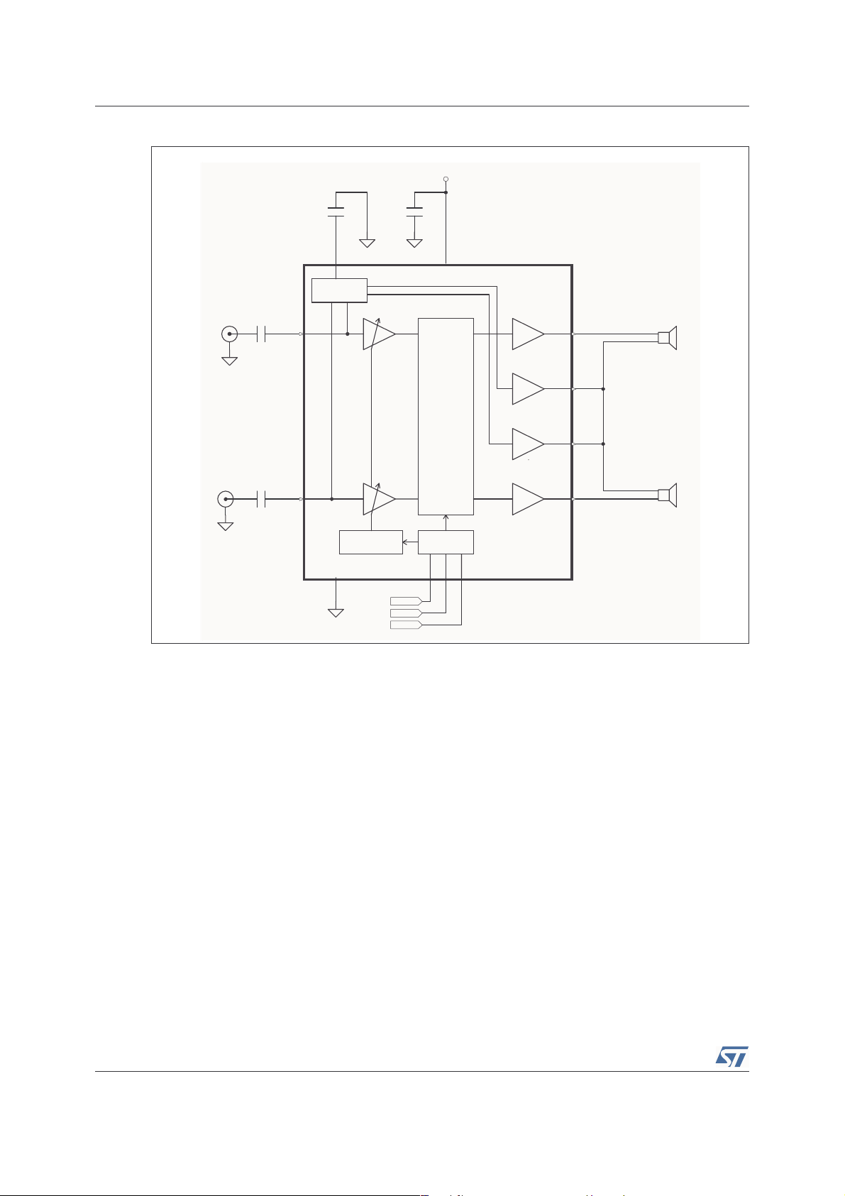
TS4975 Typical Application Schematics
2 Typical Application Schematics
Typical application schematics for the TS4975 are show in
configuration and in
Figure 2
, for a phantom ground output configuration.
Figure 1. Single-ended configuration
Vcc
IN2
IN1
Cin1
33 0nF
Cin2
33 0nF
+
Cb
1µF
A1
Bypass
Bias
IN1
Pre-Amplifier
IN1
A2
IN2
Pre-Amplifier
IN2
D2
Volume control
GND
C2
ADD
SCL
SDA
+
Cs
1µF
B2
Vcc
OUT1 Amplifier
PHG1 Amplifier
Mode
Select
ADD
D1
I2C
SCL
SDA
C1
B1
PHG2 Amplifier
OUT2 Amplifier
Figure 1
OUT1
PHG1
PHG2
OUT2
TS4975
, for a single-ended output
Cout1
+
A3
220µF
1k
B3
C3
Cout2
+
D3
220µF
1k
RL = 16/32 Ohms
+
RL = 16/32 Ohms
+
3/36
Typical Application Schematics TS4975
Figure 2. Phantom ground output configuration
Vcc
IN2
IN1
Cin1
330 nF
Cin2
330 nF
+
A1
Bypass
Cb
1µF
+
Cs
1µF
B2
Vcc
Bias
IN 1
Pre-Amplifier
IN1
A2
OUT1 Amplifier
PHG1 Amplifier
OUT1
PHG1
RL = 16 /32 Ohms
A3
B3
+
Mode
Select
IN 2
Pre-Amplifier
IN2
D2
Volume control
GND
C2
ADD
SCL
SDA
I2C
SCL
SDA
ADD
D1
C1
B1
PHG2 Amplifier
OUT2 Amplifier
TS4975
PHG2
OUT2
C3
RL = 16 /32 Ohms
D3
+
4/36
TS4975 Electrical Characteristics
3 Electrical Characteristics
Table 3. Electrical characteristics for the I²C interface
Symbol Parameter Value Unit
V
IL
V
IH
F
SCL
V
ol
I
i
1. SCL and SDA are CMOS inputs. The nominal input current is about few pA and not 10uA. 10µA refer to the I2C
bus specification.
Maximum Low level Input Voltage on pins SDA, SCL, VADD
Minimum High Level Input Voltage on pins SDA, SCL, VADD
SCL Maximum clock Frequency 400 kHz
Max Low Level Output Voltage, SDA pin, I
Max Input current on SDA, SCL
from 0.1 V
CC
to 0.9 V
CC
(1)
sink
=3mA
0.3 V
CC
0.7 V
CC
0.4 V
10 µA
Table 4. Output noise (all inputs grounded)
Unweighted Filter
from V
= 2.5V to 5V
CC
SE, G = +2dB 34µVrms 23µVrms
SE, G = +18dB 67µVrms 45µVrms
PHG, G = +2dB 34µVrms 23µVrms
PHG, G = +18dB 67µVrms 45µVrms
Weighted Filter (A)
from VCC= 2.5V to 5V
V
V
5/36

Electrical Characteristics TS4975
Table 5. VCC = +2.5 V, GND = 0V, T
= 25°C (unless otherwise specified)
amb
Symbol Parameter Conditions Min. Typ. Max. Unit
I
CC
I
STBY
V
oo
P
out
THD + N
Supply Current
Standby Current
Output Offset Voltage
Output Power
(per channel)
Total Harmonic
Distortion + Noise
No input signal, no load,
Single-ended, Mode 1-4
No input signal, no load,
Single-ended, Mode 5-8
No input signal, no load,
Phantom Ground, Mode 1-4
No input signal, no load,
Phantom Ground, Mode 5-8
SCL and SDA at V
CC
level,
No input signal
No input signal, R
=32Ω,
L
Phantom Ground
Single-ended, THD+N = 1% Max,
F=1kHz, R
=16Ω
L
Single-ended, THD+N = 1% Max,F = 1kHz,
R
=32Ω
L
Phantom Ground, THD+N = 1% Max,
F=1kHz, R
=16Ω
L
Phantom Ground, THD+N = 1% Max,
F=1kHz, R
=32Ω
L
Single-ended, AV= 2dB, RL=32Ω,
P
= 10 mW, 20Hz < F < 20kHz,
out
Single-ended, A
P
= 15 mW, 20Hz < F < 20kHz
out
Phantom Ground, A
P
= 10 mW, 20Hz < F < 20kHz
out
= 2dB, RL=16Ω,
V
= 2dB, RL=32Ω,
V
Phantom GroundAV= 2dB, RL=16Ω,
P
= 15 mW, 20Hz < F < 20kHz
out
15 21
11 13
15 21
11 13
34.2
22.8
4.6 6.5
3.6 5.3
0.6 2 µA
550mV
0.3
0.3
0.3
0.3
Single-ended Output referenced to
Phantom Ground
PSRR
Power Supply
Rejection Ratio
(1)
F = 217Hz, R
V
=200mVpp, Input Grounded,
ripple
C
= 1µF
b
Single-ended Output referenced to
=16Ω, AV= 2dB
L
60
Ground,
F = 217Hz, R
V
=200mVpp, Input Grounded,
ripple
C
= 1µF
b
=16Ω, AV= 2dB
L
60 dB
mA
mW
%
6/36

TS4975 Electrical Characteristics
Table 5. VCC = +2.5 V, GND = 0V, T
= 25°C (unless otherwise specified)
amb
Symbol Parameter Conditions Min. Typ. Max. Unit
=32Ω, AV= 2dB with Single-ended
R
Crosstalk Channel Separation
SNR
ONoise
Signal to Noise Ratio
A-Weighted
Output Noise Voltage,
A-Weighted
L
F=1kHZ, P
R
=32Ω, AV= 2dB with Single-ended
L
F = 20Hz to 20kHz, P
=32Ω, AV= 2dB with Phantom Ground,
R
L
F=1kHZ, P
= 10mW
out
= 10mW
out
out
= 10mW
RL=32Ω, AV= 2dB with Phantom Ground,
F = 20Hz to 20kHz, P
AV= 2dB, RL=32Ω, P
out
out
= 10mW
=12mW
Single-Ended
A
= 2dB, RL=32Ω, P
V
=12mW
out
Phantom Ground
A
= 2dB, Single-ended
V
= 2dB, Phantom Ground
A
V
103
75
69
69
88
88
23
µVrms
23
G Digital Gain Range In1 & In2 to Out1 & Out2 -34 +18 dB
Digital Gain Stepsize 4 dB
Gain Error Tolerance -1 +1 dB
Z
t
t
1. Dynamic measurements - 20*log(rms(V
In1 & In2 Input
in
Impedance
Wake up time
wu
Standby time 1 µs
ws
All gain settings 25.5 30 34.5 kΩ
= 1µF
C
b
)/rms(V
out
ripple
)). V
is an added sinus signal to V
ripple
110 180 ms
@ F = 217Hz
CC
dB
dB
7/36

Electrical Characteristics TS4975
Table 6. VCC = +3.3V, GND = 0V, T
= 25°C (unless otherwise specified)
amb
Symbol Parameter Conditions Min. Typ. Max. Unit
I
CC
I
STBY
V
oo
P
out
THD + N
Supply Current
Standby Current
Output Offset Voltage
Output Power
(per channel)
Total Harmonic
Distortion + Noise
No input signal, no load,
Single-ended, Mode 1-4
No input signal, no load,
Single-ended, Mode 5-8
No input signal, no load,
Phantom Ground, Mode 1-4
No input signal, no load,
Phantom Ground, Mode 5-8
SCL and SDA at V
CC
level,
No input signal
No input signal, R
=32Ω,
L
Phantom Ground
Single-ended, THD+N = 1% Max,
F=1kHz, R
=16Ω
L
Single-ended, THD+N = 1%
Max,F = 1kHz, R
=32Ω
L
Phantom Ground, THD+N = 1% Max,
F=1kHz, R
=16Ω
L
Phantom Ground, THD+N = 1% Max,
F=1kHz, R
Single-ended, A
P
= 20 mW, 20Hz < F < 20kHz,
out
Single-ended, A
P
= 30 mW, 20Hz < F < 20kHz
out
Phantom Ground, A
P
=20 mW, 20Hz < F < 20kHz
out
Phantom GroundA
P
= 30 mW, 20Hz < F < 20kHz
out
=32Ω
L
= 2dB, RL=32Ω,
V
= 2dB, RL=16Ω,
V
=2dB, RL=32Ω,
V
=2dB, RL=16Ω,
V
34 40
24 26
34 40
24 26
34.2
22.8
4.6 6.5
3.6 5.3
0.6 2 µA
550mV
0.3
0.3
0.3
0.3
Single-ended Output referenced to
Phantom Ground
PSRR
Power Supply
Rejection Ratio
(1)
F = 217Hz, R
V
= 200mVpp, Input Grounded,
ripple
C
= 1µF
b
Single-ended Output referenced to
=16Ω, AV=2dB
L
61
Ground,
F = 217Hz, R
V
= 200mVpp, Input Grounded,
ripple
C
= 1µF
b
=16Ω, AV=2dB
L
61
mA
mW
%
dB
8/36
TS4975 Electrical Characteristics
Table 6. VCC = +3.3V, GND = 0V, T
= 25°C (unless otherwise specified)
amb
Symbol Parameter Conditions Min. Typ. Max. Unit
R
=32Ω, AV= 2dB with Single-ended
Crosstalk Channel Separation
SNR Signal To Noise Ratio
ONoise
Output Noise Voltage,
A-Weighted
L
F=1kHZ, P
=32Ω, AV= 2dB with Single-ended
R
L
F = 20Hz to 20kHz, P
=32Ω, AV= 2dB with Phantom Ground,
R
L
F=1kHZ, P
=32Ω, AV= 2dB with Phantom Ground,
R
L
F = 20Hz to 20kHz, P
=2dB, RL=32Ω, P
A
V
=20mW
out
=20mW
out
=20mW
out
=20mW
out
= 25mW
out
Single-Ended
A
=2dB, RL=32Ω, P
V
= 25mW
out
Phantom Ground
A
= 2dB, Single-ended
V
= 2dB, Phantom Ground
A
V
103
75
69
69
90
90
23
23
G Digital Gain Range In1 & In2 to Out1 & Out2 -34 +18 dB
Digital Gain Step size 4 dB
Gain Error Tolerance -1 +1 dB
in
In1 & In2 Input
Impedance
Wake up time
All gain settings 25.5 30 34.5 kΩ
C
=1µF
b
90 156 ms
Standby time 1 µs
)/rms(V
out
ripple
)). V
is an added sinus signal to VCC @ F = 217Hz
ripple
Z
t
wu
t
ws
1. Dynamic measurements - 20*log(rms(V
dB
dB
µVrms
9/36

Electrical Characteristics TS4975
Table 7. VCC = +5V, GND = 0V, T
= 25°C (unless otherwise specified)
amb
Symbol Parameter Conditions Min. Typ. Max. Unit
I
CC
I
STBY
V
oo
P
out
THD + N
Supply Current
Standby Current
Output Offset Voltage
Output Power
(per channel)
Tot al H ar mo n ic
Distortion + Noise
No input signal, no load,
Single-ended, Mode 1-4
No input signal, no load,
Single-ended, Mode 5-8
No input signal, no load,
Phantom Ground, Mode 1-4
No input signal, no load,
Phantom Ground, Mode 5-8
SCL and SDA at V
CC
level,
No input signal
No input signal, R
=32Ω,
L
Phantom Ground
Single-ended, THD+N = 1% Max,
F=1kHz, R
=16Ω
L
Single-ended, THD+N = 1%
Max,F = 1kHz, R
=32Ω
L
Phantom Ground, THD+N = 1% Max,
F=1kHz, R
=16Ω
L
Phantom Ground, THD+N = 1% Max,
F=1kHz, R
Single-ended, A
P
= 50 mW, 20Hz < F < 20kHz,
out
Single-ended, A
P
= 80 mW, 20Hz < F < 20kHz
out
=32Ω
L
= 2dB, RL=32Ω,
V
= 2dB, RL=16Ω,
V
Phantom Ground, AV=2dB, RL=32Ω,
P
=50 mW, 20Hz < F < 20kHz
out
Phantom GroundAV= 2dB, RL=16Ω,
P
= 80 mW, 20Hz < F < 20kHz
out
92 102
59 64
92 98
59 63
34.2
22.8
4.6 6.5
3.6 5.3
0.6 2 µA
550mV
0.3
0.3
0.3
0.3
Single-ended Output referenced to
Phantom Ground
PSRR
Power Supply
Rejection Ratio
(1)
F = 217Hz, R
V
= 200mVpp, Input Grounded,
ripple
C
=1µF
b
Single-ended Output referenced to
=16Ω, AV=2dB
L
63
Ground
F = 217Hz, R
V
= 200mVpp, Input Grounded,
ripple
C
=1µF
b
=16Ω, AV=2dB
L
63
mA
mW
%
dB
10/36

TS4975 Electrical Characteristics
Table 7. VCC = +5V, GND = 0V, T
= 25°C (unless otherwise specified)
amb
Symbol Parameter Conditions Min. Typ. Max. Unit
=32Ω, AV= 2dB with Single-ended
R
Crosstalk Channel Separation
SNR
Signal To Noise
Ratio, A-Weighted
Output Noise
ONoise
Voltage,
A-Weighted
L
F=1kHZ, P
=32Ω, AV= 2dB with Single-ended
R
L
F = 20Hz to 20kHz, P
=50mW
out
=50mW
out
RL=32Ω, AV= 2dB with Phantom Ground,
F=1kHZ, P
=50mW
out
RL=32Ω, AV= 2dB with Phantom Ground,
F = 20Hz to 20kHz, P
=2dB, RL=32Ω, P
A
V
=50mW
out
= 62mW
out
Single-Ended
A
=2dB, RL=32Ω, P
V
= 62mW
out
Phantom Ground
A
= 2dB, Single-ended
V
= 2dB, Phantom Ground
A
V
103
75
69
69
95
95
23
µVrms
23
G Digital Gain Range In1 & In2 to Out1 & Out2 -34 +18 dB
Digital Gain Step size 4 dB
Gain Error Tolerance -1 +1 dB
wu
ws
in
In1 & In2 Input
Impedance
Wake up time
All gain settings 25.5 30 34.5 kΩ
C
=1µF
b
80 144 ms
Standby time 1 µs
ripple
)). V
is an added sinus signal to VCC @ F = 217Hz
ripple
Z
t
t
1. Dynamic measurements - 20*log(rms(Vout)/rms(V
dB
dB
11/36

Electrical Characteristics TS4975
Figure 3. THD+N vs. output power Figure 4. THD+N vs. output power
10
RL = 8
Ω
Out. mode 1 - 8
SE, G = +2dB
BW < 125kHz
1
Tamb = 25°C
0.1
THD + N (%)
0.01
Vcc=3.3V
F=1kHz
1E-3
1E-3 0. 01 0.1
Vcc=2.5V
F=20kHz
Vcc=2.5V
F=1kHz
Vcc=3.3V
F=20kHz
Vcc=5V
F=20kHz
Output power (W)
Vcc=5V
F=1kHz
10
RL = 8
Ω
Out. mode 1 - 8
SE, G = +18dB
BW < 125kHz
1
Tamb = 25°C
0.1
THD + N (%)
0.01
1E-3
Vcc=2.5V
F=1kHz
1E-3 0. 01 0.1
Vcc=3.3V
F=20kHz
Vcc=2.5V
F=20kHz
Vcc=3.3V
F=1kHz
Vcc=5V
F=20kHz
Output power (W)
Figure 5. THD+N vs. output power Figure 6. THD+N vs. output power
10
0.1
THD + N (%)
0.01
RL = 16
Out. mode 1 - 8
SE, G = +2dB
BW < 125kHz
1
Tamb = 25°C
Vcc=3.3V
F=1kHz
Ω
Vcc=2.5V
F=20kHz
Vcc=2.5V
F=1kHz
Vcc=3.3V
F=20kHz
Vcc=5V
F=20kHz
Vcc=5V
F=1kHz
10
0.1
THD + N (%)
0.01
RL = 16
Out. mode 1 - 8
SE, G = +18dB
BW < 125kHz
1
Tamb = 25°C
Vcc=2.5V
F=20kHz
Ω
Vcc=3.3V
F=20kHz
Vcc=2.5V
F=1kHz
Vcc=3.3V
F=1kHz
Vcc=5V
F=20kHz
Vcc=5V
F=1kHz
Vcc=5V
F=1kHz
1E-3
1E-3 0.01 0. 1
Output power (W)
1E-3
1E-3 0.01 0. 1
Output power (W)
Figure 7. THD+N vs. output power Figure 8. THD+N vs. output power
10
RL = 32
Ω
Out. mode 1 - 8
SE, G = +2dB
BW < 125kHz
1
Tamb = 25°C
0.1
THD + N (%)
0.01
Vcc=2.5V
F=1kHz
1E-3
1E-3 0.01 0. 1
Vcc=3.3V
F=20kHz
Output power (W)
Vcc=3.3V
F=1kHz
Vcc=2.5V
F=20kHz
Vcc=5V
F=20kHz
Vcc=5V
F=1kHz
10
RL = 32
Ω
Out. mode 1 - 8
SE, G = +18dB
BW < 125kHz
1
Tamb = 25°C
0.1
THD + N (%)
0.01
Vcc=2.5V
F=1kHz
1E-3
1E-3 0.01 0. 1
Vcc=3.3V
F=20kHz
Output power (W)
Vcc=3.3V
F=1kHz
Vcc=2.5V
F=20kHz
Vcc=5V
F=20kHz
Vcc=5V
F=1kHz
12/36

TS4975 Electrical Characteristics
Figure 9. THD+N vs. output power Figure 10. THD+N vs. output power
10
RL = 8
Ω
Out. mode 1 - 8
PHG, G = +2dB
BW < 125kHz
1
Tamb = 25°C
0.1
THD + N (%)
0.01
Vcc=3.3V
F=1kHz
1E-3
1E-3 0.01 0. 1
Vcc=2.5V
F=20kHz
Vcc=2.5V
F=1kHz
Vcc=3.3V
F=20kHz
Output power (W)
Vcc=5V
F=20kHz
Vcc=5V
F=1kHz
10
Ω
Vcc=2.5V
F=20kHz
Vcc=2.5V
F=1kHz
1
0.1
THD + N (%)
RL = 8
0.01
Out. mode 1 - 8
SE, G = +18dB
BW < 125kHz
Tamb = 25°C
1E-3
1E-3 0.01 0. 1
Vcc=3.3V
F=20kHz
Vcc=3.3V
F=1kHz
Vcc=5V
F=20kHz
Output power (W)
Figure 11. THD+N vs. output power Figure 12. THD+N vs. output power
10
RL = 16
Ω
Out. mode 1 - 8
PHG, G = +2dB
BW < 125kHz
1
Tamb = 25°C
0.1
THD + N (%)
0.01
Vcc=3.3V
F=1kHz
1E-3
1E-3 0.01 0. 1
Vcc=2.5V
F=20kHz
Vcc=2.5V
F=1kHz
Vcc=3.3V
F=20kHz
Output power (W)
Vcc=5V
F=20kHz
Vcc=5V
F=1kHz
10
Vcc=2.5V
F=1kHz
1
0.1
THD + N (%)
RL = 16
0.01
1E-3
1E-3 0.01 0. 1
Ω
Out. mode 1 - 8
PHG, G = +18dB
BW < 125kHz
Tamb = 25°C
Vcc=3.3V
F=20kHz
Vcc=2.5V
F=20kHz
Vcc=3.3V
F=1kHz
Vcc=5V
F=20kHz
Output power (W)
Vcc=5V
F=1kHz
Vcc=5V
F=1kHz
Figure 13. THD+N vs. output power Figure 14. THD+N vs. output power
10
RL = 32
Ω
Out. mode 1 - 8
PHG, G = +2dB
BW < 125kHz
1
Tamb = 25°C
0.1
THD + N (%)
0.01
Vcc=2.5V
F=1kHz
1E-3
1E-3 0.01 0. 1
Vcc=3.3V
F=20kHz
Output power (W)
Vcc=3.3V
F=1kHz
Vcc=2.5V
F=20kHz
Vcc=5V
F=20kHz
Vcc=5V
F=1kHz
10
RL = 32
Ω
Out. mode 1 - 8
PHG, G = +18dB
BW < 125kHz
1
Tamb = 25°C
0.1
THD + N (%)
Vcc=2.5V
0.01
F=1kHz
1E-3
1E-3 0.01 0. 1
Vcc=3.3V
F=20kHz
Output power (W)
Vcc=3.3V
F=1kHz
Vcc=2.5V
F=20kHz
Vcc=5V
F=20kHz
Vcc=5V
F=1kHz
13/36

Electrical Characteristics TS4975
Figure 15. THD+N vs. frequency Figure 16. THD+N vs. frequency
10
1
THD + N (%)
0.1
0.01
RL = 8
Ω
Output mode 1 - 8
Single Ended
G = +2dB
BW < 125kHz
Tamb = 25°C
Vcc=2.5V
P=20mW
100 1000 10000
Vcc=3.3V
P=40mW
Frequency (Hz)
Vcc=5V
P=110mW
10
1
THD + N (%)
0.1
0.01
RL = 8
Ω
Output mode 1 - 8
Single Ended
G = +18dB
BW < 125kHz
Tamb = 25°C
Vcc=2.5V
P=20mW
100 1000 10000
Vcc=3.3V
P=40mW
Frequency (Hz)
Figure 17. THD+N vs. frequency Figure 18. THD+N vs. frequency
10
1
THD + N (%)
0.1
RL = 16
Ω
Output mode 1 - 8
Single Ended
G = +2dB
BW < 125kHz
Tamb = 25°C
Vcc=2.5V
P=15mW
Vcc=3.3V
P=30mW
Vcc=5V
P=80mW
10
1
THD + N (%)
0.1
RL = 16
Ω
Output mode 1 - 8
Single Ended
G = +18dB
BW < 125kHz
Tamb = 25°C
Vcc=2.5V
P=15mW
Vcc=3.3V
P=30mW
Vcc=5V
P=110mW
Vcc=5V
P=80mW
0.01
100 1000 10000
Frequency (Hz)
0.01
100 1000 10000
Frequency (Hz)
Figure 19. THD+N vs. frequency Figure 20. THD+N vs. frequency
10
1
THD + N (%)
0.1
0.01
RL = 32
Ω
Output mode 1 - 8
Single Ended
G = +2dB
BW < 125kHz
Tamb = 25°C
Vcc=2.5V
P=10mW
100 1000 10000
Vcc=3.3V
P=20mW
Frequency (Hz)
Vcc=5V
P=50mW
10
1
THD + N (%)
0.1
0.01
RL = 32
Ω
Output mode 1 - 8
Single Ended
G = +18dB
BW < 125kHz
Tamb = 25°C
Vcc=2.5V
P=10mW
100 1000 10000
Vcc=3.3V
P=20mW
Frequency (Hz)
Vcc=5V
P=50mW
14/36

TS4975 Electrical Characteristics
Figure 21. THD+N vs. frequency Figure 22. THD+N vs. frequency
10
1
THD + N (%)
0.1
0.01
RL = 8
Ω
Output mode 1 - 8
Phantom Ground
G = +2dB
BW < 125kHz
Tamb = 2 5°C
Vcc=2.5V
P=20mW
100 1000 10000
Vcc=3.3V
P=40mW
Frequency (Hz)
Vcc=5V
P=110mW
10
1
THD + N (%)
0.1
0.01
RL = 8
Ω
Output mode 1 - 8
Phantom Ground
G = +18dB
BW < 125kHz
Tamb = 2 5°C
Vcc=2.5V
P=20mW
100 1000 10000
Vcc=3.3V
P=40mW
Frequency (Hz)
Figure 23. THD+N vs. frequency Figure 24. THD+N vs. frequency
10
1
THD + N (%)
0.1
RL = 16
Ω
Output mode 1 - 8
Phantom Ground
G = +2dB
BW < 125kHz
Tamb = 25°C
Vcc=2.5V
P=15mW
Vcc=3.3V
P=30mW
Vcc=5V
P=80mW
10
1
THD + N (%)
0.1
RL = 16
Ω
Output mode 1 - 8
Phantom Ground
G = +18dB
BW < 125kHz
Tamb = 25°C
Vcc=2.5V
P=15mW
Vcc=3.3V
P=30mW
Vcc=5V
P=110mW
Vcc=5V
P=80mW
0.01
100 1000 10000
Frequency (Hz)
0.01
100 1000 10000
Frequency (Hz)
Figure 25. THD+N vs. frequency Figure 26. THD+N vs. frequency
10
1
THD + N (%)
0.1
0.01
RL = 32
Ω
Output mode 1 - 8
Phantom Ground
G = +2dB
BW < 125kHz
Tamb = 2 5°C
Vcc=2.5V
P=10mW
100 1000 10000
Vcc=3.3V
P=20mW
Frequency (Hz)
Vcc=5V
P=50mW
10
1
THD + N (%)
0.1
0.01
RL = 32
Ω
Output mode 1 - 8
Phantom Ground
G = +18dB
BW < 125kHz
Tamb = 25°C
Vcc=2.5V
P=10mW
100 1000 10000
Vcc=3.3V
P=20mW
Frequency (Hz)
Vcc=5V
P=50mW
15/36

Electrical Characteristics TS4975
Figure 27. Output power vs. power supply
voltage (each channel)
180
F = 1kHz
160
Output mode 1 - 8
Single Ended
140
BW < 125 kHz
Tamb = 25°C
120
100
80
60
40
20
Output power at 1% THD + N (mW)
0
2.53.03.54.04.55.05.5
32
Ω
Vcc (V)
8
Ω
16
Ω
64
Ω
Figure 29. Output power vs. power supply
voltage (each channel)
180
F = 1kHz
160
Output mode 1 - 8
Phantom Ground
140
BW < 125 kHz
Tamb = 25°C
120
100
80
60
40
20
Output power at 1% THD + N (mW)
0
2.53.03.54.04.55.05.5
32
Ω
Vcc (V)
8
Ω
16
Ω
64
Ω
Figure 28. Output power vs. power supply
voltage (each channel)
220
F = 1kHz
200
Output mode 1 - 8
180
Single Ended
BW < 125 kHz
160
Tamb = 25°C
140
120
100
80
60
40
20
Output power at 10% THD + N (mW)
0
2.53.03.54.04.55.05.5
32
Ω
Vcc (V)
8
Ω
16
Ω
64
Ω
Figure 30. Output power vs. power supply
voltage (each channel)
220
F = 1kHz
200
Output mode 1 - 8
180
Phantom Ground
BW < 125 kHz
160
Tamb = 25°C
140
120
100
80
60
40
20
Output power at 10% THD + N (mW)
0
2.53.03.54.04.55.05.5
32
Ω
Vcc (V)
8
Ω
16
Ω
64
Ω
16/36

TS4975 Electrical Characteristics
Figure 31. PSSR vs. frequency Figure 32. PSSR vs. frequency
0
Vcc = 2.5V
-10
RL ≥ 16
-20
-30
-40
-50
PSRR (dB)
-60
-70
-80
-90
-100
20
Ω
Output mode 1 - 8
SE, Inp. grounded
Vripple = 200mVpp
G=+10dB
G=-10dB
100 1000 10000
G=+18dB
G=+2dB
G=-34dB
G=-2dB
Frequency (Hz)
0
Vcc = 2.5V
-10
RL ≥ 16
-20
-30
-40
-50
PSRR (dB)
-60
-70
-80
-90
-100
20
Ω
Output mode 1 - 8
PHG, Inp. grounded
Vripple = 200mVpp
G=+10dB
100 1000 10000
G=+2dB
G=-10dBG=-2dB
Frequency (Hz)
Figure 33. PSSR vs. frequency Figure 34. PSSR vs. frequency
-10
-20
-30
-40
-50
PSRR (dB)
-60
-70
-80
-90
-100
0
Vcc = 3.3V
RL ≥ 16
Ω
Output mode 1 - 8
SE, Inp. grounded
Vripple = 200mVpp
G=-10dB
20
G=+18dB
G=+10dB
G=-2dB
100 1000 10000
G=+2dB
G=-34dB
Frequency (Hz)
0
Vcc = 3.3V
-10
RL ≥ 16
-20
-30
-40
-50
PSRR (dB)
-60
-70
-80
-90
-100
20
Ω
Output mode 1 - 8
PHG, Inp. grounded
Vripple = 200mVpp
G=+10dB
100 1000 10000
G=+2dB
G=-10dBG=-2dB
Frequency (Hz)
G=+18dB
G=-34dB
G=+18dB
G=-34dB
Figure 35. PSSR vs. frequency Figure 36. PSSR vs. frequency
-10
-20
-30
-40
-50
PSRR (dB)
-60
-70
-80
-90
-100
0
Vcc = 5V
RL ≥ 16
Ω
Output mode 1 - 8
SE, Inp. grounded
Vripple = 200mVpp
G=-10dB
20
G=+18dB
G=+10dB
100 1000 10000
G=+2dB
G=-2dB
Frequency (Hz)
G=-34dB
0
-10
-20
-30
-40
-50
PSRR (dB)
-60
-70
-80
-90
-100
Vcc = 5V
RL ≥ 16
Ω
Output mode 1 - 8
PHG, Inp. grounded
Vripple = 200mVpp
20
100 1000 10000
G=+10dB
G=-2dB
Frequency (Hz)
G=+2dB
G=-10dB
G=+18dB
G=-34dB
17/36

Electrical Characteristics TS4975
Figure 37. Crosstalk vs. frequency Figure 38. Crosstalk vs. frequency
0
Vcc = 2.5V
Output mode 1
-10
Phantom Ground
G = +2dB
-20
Tamb = 25°C
-30
-40
-50
Crosstalk Level (dB)
-60
-70
-80
RL=32
Ω
Po=10mW
100 1000 10000
Frequency (Hz)
RL=16
Po=15mW
Crosstalk Level (dB)
-20
-40
-60
-80
-100
-120
0
Vcc = 2.5V
Output mode 1
Single Ended
G = +2dB
Tamb = 25°C
RL=16
Ω
RL=32
Po=10mW
100 1000 10000
Frequency (Hz)
Po=15mW
Ω
Figure 39. Crosstalk vs. frequency Figure 40. Crosstalk vs. frequency
0
Vcc = 3.3V
Output mode 1
-10
Phantom Ground
G = +2dB
-20
Tamb = 25°C
-30
-40
-50
Crosstalk Level (dB)
-60
-70
-80
RL=32
Ω
Po=20mW
100 1000 10000
Frequency (Hz)
RL=16
Po=30mW
Crosstalk Level (dB)
-20
-40
-60
-80
-100
-120
0
Vcc = 3.3V
Output mode 1
Single Ended
G = +2dB
Tamb = 25°C
RL=16
Ω
RL=32
Po=20mW
100 1000 10000
Frequency (Hz)
Po=30mW
Ω
Ω
Ω
Figure 41. Crosstalk vs. frequency Figure 42. Crosstalk vs. frequency
0
Vcc = 5V
Output mode 1
-20
Single Ended
G = +2dB
Tamb = 25°C
-40
RL=16
Ω
Po=80mW
Crosstalk Level (dB)
-60
-80
-100
-120
RL=32
Ω
Po=50mW
100 1000 10000
Frequency (Hz)
18/36
0
Vcc = 5V
Output mode 1
-10
Phantom Ground
G = +2dB
-20
Tamb = 25°C
-30
-40
-50
Crosstalk Level (dB)
-60
-70
-80
RL=32
Ω
Po=50mW
100 1000 10000
Frequency (Hz)
RL=16
Po=80mW
Ω

TS4975 Electrical Characteristics
Figure 43. SNR vs. power supply voltage Figure 44. SNR vs. power supply voltage
110
108
106
104
102
100
98
96
94
92
SNR (dB)
90
88
86
84
82
80
RL = 32
RL = 16
Out. mode 1 - 8
SE, G = +2dB
Unweighted filter (20Hz to 20kHz)
THD+N < 0.5%
Tamb = 25°C
2.5 3.3 5
Ω
Ω
Vcc (V)
110
108
106
104
Out. mode 1 - 8
102
SE, G = +2dB
100
Weighted filter type A
98
THD+N < 0.5%
96
Tamb = 25°C
94
92
SNR (dB)
90
88
86
84
82
80
RL = 32
Ω
RL = 16
Ω
2.5 3.3 5
Vcc (V)
Figure 45. SNR vs. power supply voltage Figure 46. SNR vs. power supply voltage
110
108
106
104
102
100
98
96
94
92
90
88
86
SNR (dB)
84
82
80
78
76
74
72
70
RL = 32
Ω
RL = 16
Out. mode 1 - 8
SE, G = +18dB
Unweighted filter (20Hz to 20kHz)
THD+N < 0.5%
Tamb = 25°C
2.5 3.3 5
Ω
Vcc (V)
110
108
106
104
102
Out. mode 1 - 8
100
98
SE, G = +18dB
96
Weighted filter type A
94
THD+N < 0.5%
92
Tamb = 25°C
90
88
86
SNR (dB)
84
82
80
78
76
74
72
70
RL = 32
Ω
RL = 16
Ω
2.5 3.3 5
Vcc (V)
Figure 47. SNR vs. power supply voltage Figure 48. SNR vs. power supply voltage
110
108
106
104
102
100
98
96
94
92
SNR (dB)
90
88
86
84
82
80
RL = 32
Ω
RL = 16
Out. mode 1 - 8
PHG, G = +2dB
Unweighted filter (20Hz to 20kHz)
THD+N < 0.5%
Tamb = 25°C
2.5 3.3 5
Ω
Vcc (V)
110
108
106
104
Out. mode 1 - 8
102
PHG, G = +2dB
100
Weighted filter type A
98
THD+N < 0.5%
96
Tamb = 25°C
94
92
SNR (dB)
90
88
86
84
82
80
RL = 32
Ω
RL = 16
Ω
2.5 3.3 5
Vcc (V)
19/36

Electrical Characteristics TS4975
Figure 49. SNR vs. power supply voltage Figure 50. SNR vs. power supply voltage
110
108
106
104
102
100
98
96
94
92
90
88
86
SNR (dB)
84
82
80
78
76
74
72
70
RL = 32
RL = 16
Out. mode 1 - 8
PHG, G = +18dB
Unweighted filter (20Hz to 20kHz)
THD+N < 0.5%
Tamb = 25°C
2.5 3.3 5
Ω
Ω
Vcc (V)
110
108
106
104
102
Out. mode 1 - 8
100
98
PHG, G = +18dB
96
Weighted filter type A
94
THD+N < 0.5%
92
Tamb = 25°C
90
88
86
SNR (dB)
84
82
80
78
76
74
72
70
RL = 32
Ω
RL = 16
Ω
2.5 3.3 5
Vcc (V)
Figure 51. Frequency response Figure 52. Current consumption vs. power
supply voltage
20
18
16
14
12
10
8
6
Output level (dB)
4
2
0
20
Vcc = 5V, 3.3V, 2.5V
G = +18dB
Vcc = 5V, 3.3V, 2.5V
G = +2dB
100 1000 10000
Frequency (Hz)
Output mode 1 - 8
RL = 32, 16
Cin = 330nF
SE, PHG
BW < 125kHz
Tamb = 25°C
Ω
6
No loads
Tamb = 25°C
5
4
3
Icc (mA)
Reset state
2
1
0
012345
PHG, Out. Mode 1, 2, 3, 4
PHG, Out. mode 5, 6 , 7, 8
SE, Out. m ode 1, 2, 3, 4
SE, Out. mode 5, 6, 7, 8
Vcc (V)
Figure 53. 3dB lower cut off frequency vs.
input capacitance
100
Typical Input
Impedance
10
Maximum Input
Low -3dB Cut Off Frequency (Hz)
0.1
Impedance
Input Capacitor Cin (µF)
20/36
All gain setting
Tamb=25°C
Minimum Input
Impedance
1
Figure 54. 3dB lower cut off frequency vs.
output capacitance
100
10
Low -3 dB Cut Off frequency (Hz)
1
100 1000
RL=16
Ω
RL=32
Output capacitor Cout (µF)
Ω
All gain setting
Tamb = 25°C

TS4975 Electrical Characteristics
Figure 55. Power dissipation vs. output power
(one channel
70
Vcc = 2.5V
F = 1kHz
60
THD+N < 1%
50
40
30
20
Power Dissipation (mW)
10
0
0 5 10 15 20 25
Output Power (mW)
RL=16Ω, PHG
RL=32Ω, PHG
RL=16Ω, SE
RL=32Ω, SE
Figure 57. Power dissipation vs. output power
(one channel
280
Vcc = 5V
260
F = 1kHz
240
THD+N < 1%
220
200
180
160
140
120
100
80
60
Power Dissipation (mW)
40
20
0
0 102030405060708090100110
Output Power (mW)
RL=16Ω, PHG
RL=32Ω, PHG
RL=16Ω, SE
RL=32Ω, SE
Figure 56. Power dissipation vs. output power
(one channel
120
Vcc = 3.3V
110
F = 1kHz
100
THD+N < 1%
90
80
70
60
50
40
30
Power Dissipation (mW)
20
10
0
0 5 10 15 20 25 30 35 40 45
Output Power (mW)
RL=16Ω, PHG
RL=32Ω, PHG
RL=16Ω, SE
RL=32Ω, SE
Figure 58. Power derating curves
1.4
1.2
1.0
0.8
0.6
0.4
0.2
Flip-Chip Package Power D issipation (W)
0.0
No Heat sink
0 25 50 75 100 125 150
Ambiant Temperature (°C)
Heat sink surface = 125mm
2
21/36

Application Information TS4975
4 Application Information
The TS4975 integrates 2 monolithic power amplifiers. The amplifier output can be configured
as either SE (single-ended) capacitively-coupled output or PHG (phantom ground) output.
Figure 1 on page 3
Section 4.2: Output configuration
This chapter gives information on how to configure the TS4975 in application.
4.1 I²C bus interface
The TS4975 uses a serial bus, which conforms to the I²C protocol (the TS4975 must be
powered when it is connected to I²C bus), to control the chip’s functions with two wires: Clock
and Data. The Clock line and the Data line are bi-directional (open-collector) with an external
chip pull-up resistor (typically 10 kOhm). The maximum clock frequency in Fast-mode specified
by the I²C standard is 400kHz, which TS4975 supports. In this application, the TS4975 is
always the slave device and the controlling micro controller MCU is the master device.
The ADD pin is allows one to set one of two possible 7-bit device addresses. This setting is
needed for when a number of chips are connected to the same bus (for example two TS4975
devices), to avoid address conflicts. The two possible TS4975 addresses are:
● $CCh when the ADD pin is connected to logic low voltage,
● $CEh when ADD pin is connected to logic high voltage.
and
Figure 2 on page 4
show schemes of these two configurations and
describes these configurations.
Tabl e 8
Table 8. I²C bus interface pin descriptions
summarizes the pin descriptions for the I²C bus interface.
Pin Functional Description
SDA This is the serial data pin
SCL This is the clock input pin
ADD User-setable portion of device’s I2C address
4.1.1 I²C bus operation
The host MCU can write into the TS4975 control register to control the TS4975, and read from
the control register to get a configuration from the TS4975. The TS4975 is addressed by the
byte consisting of 7-bit slave address and R/W bit.
Table 9. The first byte after the START message for addressing the device
A6 A5 A4 A3 A2 A1 A0 R/W
1100 11A0X
In order to write data into the TS4975, after the “start” message, the MCU must send the
following data:
● send byte with the I²C 7-bit slave address and with a low level for the R/W bit
● send the data (control register setting)
22/36

TS4975 Application Information
All bytes are sent with MSB bit first. The transfer of written data ends with a “stop” message.
When transmitting several data, the data can be written with no need to repeat the “start”
message and addressing byte with the slave address.
In order to read data from the TS4975, after the “start” message, the MCU must send and
receive the following data:
● send byte with the I²C 7-bit slave address and with a high level for the R/W bit
● receive the data (control register value)
All bytes are read with MSB bit first. The transfer of read data is ended with “stop” message.
When transmitting several data, the data can be read with no need to repeat the “start”
message and the byte with slave address. In this case the value of control register is read
repeatedly.
When the thermo shutdown or pop and click reduction is active, specific values are read from
the TS4975 (see
shutdown on page 32
Section 4.9: Pop and click performance on page 31
).
Figure 59. I²C write/read operations
SLAVE ADDRESS CONTROL REGISTERS
SLAVE ADDRESS CONTROL REGISTERS
and
Section 4.10: Thermo
SDA
SDA
Start condition
Start condition
S1100
S1100
S1100
A00A
1 1 D7 D6 D5 D4D2D3
1 1 D7 D6 D5 D4D2D3
1 1 D7 D6 D5 D4D2D3
Volume Control
Volume Control
settings
settings
R/W
R/WR/W
Acknowledge
Acknowledge
from Slave
from Slave
Phantom Ground
Phantom Ground
settings
settings
Output
Output
Mode settings
Mode settings
D0D1A P
D0D1A P
D0D1A P
Acknowledge
Acknowledge
from Slave
from Slave
Stop condition
Stop condition
A00A
A00A
Table 10. Ouput mode selection: G from -34 dB to + 18dB (by steps of 4dB)
Output Mode # Headphone Output 1 Headphone Output 2
0SD SD
1 G x In1 G x In2
2 G x In2 G x In1
3 G x In1 G x In1
4 G x In2 G x In2
5SD G x In1
6SD G x In2
7 G x In1 SD
8 G x In2 SD
1. SD = Shutdown Mode
In1 = Audio Input 1
In2= Audio Input2
G = Gain from Audio Input 1and Input 2 to Output1 and Output2
(1)
23/36

Application Information TS4975
4.1.2 Gain setting operation
The gain of the TS4975 ranges from -34dB to +18 dB. At Power-up, both the right and left
channels are set in Standby mode.
Table 11. Gain settings truth table
G: Gain (dB) #
-34 0001
-30 0010
-26 0011
-22 0100
-18 0101
-14 0110
-10 0111
-6 1000
-2 1001
+2 1010
+6 1011
+10 1100
+14 1101
+18 1110
D7
(MSB)
Table 12. Output mode settings truth table
D3: PHG
on / off
D2 D1 D0 COMMENTS
D6 D5 D4
0 XXX PHG off
1 xxx PHG on
x 000 MODE 1
X 001 MODE 2
X 010 MODE 3
X 011 MODE4
X 100 MODE 5
X 101 MODE 6
X 110 MODE 7
X 111 MODE 8
Table 13. Stand-by mode I²C condition
D7
(MSB)
0 000XXXX
24/36
D6 D5 D4 D3 D2 D1 D0

TS4975 Application Information
Table 14. I²C control byte states
D7
(MSB)
1 1 1 1 x X X X Undefined State
D6 D5 D4 D3 D2 D1 D0
4.1.3 Acknowledge
The number of data bytes transferred between the start and the stop conditions from the CPU
master to the TS4975 slave is not limited. Each byte of eight bits is followed by one
acknowledge bit.
The TS4975 which is addressed, generates an acknowledge after the reception of each byte
that has been clocked out.
4.2 Output configuration
When the device is switched to Mode 5,6,7 or 8, where one channel is in shutdown, it means
that corresponding output is in a high impedance state.
4.2.1 Single-ended configuration
When the device is woken-up or switched via I²C interface to SE configuration, output amplifiers
are biased to the V
PHG1 and PHG2 are in high impedance state. In this configuration an output capacitor, C
each output is needed to block the V
/2 voltage and this voltage is present on OUT1 and OUT2 pins. Pins
CC
/2 voltage and couples the audio signal to the load.
CC
out
, on
4.2.2 Phantom ground configuration
In a PHG configuration the internal buffers are connected to PHG1 and PHG2 pins and biased
to the V
/2 voltage. Output amplifiers (pins OUT1 and OUT2) are also biased to the VCC/2
CC
voltage. Therefore, no output capacitors are needed. The advantage of the PHG configuration
is the need for fewer external components as compared with a SE configuration. However, note
that the device has higher power dissipation (see
on page 26
).
In this configuration, PHG1 and PHG2 pins must be shorted and the connection between these
pins should be as short as possible. For best crosstalk results, in this case, each speaker
should be connected with a separate PHG wire (2 speakers connected with 4 wires) as shown
in
Figure 2: Phantom ground output configuration on page 4
common PHG wire for both speakers (i.e. 2 speakers connected with 3 wires), which would give
much poorer crosstalk results.
4.2.3 Shutdown
When the device goes to shutdown from SE or PHG mode, PHG1 and PHG2 outputs are in a
high impedance state and OUT1 and OUT2 outputs are shorted together and connected to
bias voltage. This voltage steadily decreases as the bypass capacitor C
reaches GND voltage when C
implemented to reach the best pop performance during chip wake-up.
is fully discharged. This output configuration is
bypass
Section 4.3: Power dissipation and efficiency
. You should avoid using only one
discharges, and
b
25/36

Application Information TS4975
4.3 Power dissipation and efficiency
Hypotheses:
● Voltage and current in the load are sinusoidal (V
● Supply voltage is a pure DC source (V
CC
).
out
and I
out
).
Regarding the load we have:
V
outVPEAK
ωt V()sin=
and
V
out
----------- A()=
I
out
R
L
and
2
V
P
out
----------------- A()=
PEAK
2R
L
Single-ended configuration:
The average current delivered by the supply voltage is:
π
V
1
PEAK
------
Icc
AVG
------------- ---- t()sin td
∫
2π
R
L
0
Figure 60. Current delivered by supply voltage in single-ended model
V
PEAK
----------------- A()==
πR
L
The power delivered by supply voltage is:
P
supplyVCCICC
So, the power dissipation by each amplifier is
P
diss
2V
------------- ------P
π R
supplyPout
CC
L
P
P
diss
and the maximum value is obtained when:
∂P
diss
P
∂
out
26/36
W()=
AVG
W()–=
outPout
0=
W() –=

TS4975 Application Information
and its value is:
2
V
out
------------- W()=
π2R
CC
L
πV
PEAK
---------- -----------==
2V
CC
P
diss
MAX
Note: This maximum value depends only on power supply voltage and load values.
The efficiency is the ratio between the output power and the power supply:
P
------------ -------
η
P
supply
The maximum theoretical value is reached when V
π
η
--- 78.5%==
4
= VCC/2, so
PEAK
Phantom ground configuration:
The average current delivered by the supply voltage is:
π
V
1
Icc
AVG
PEAK
---
--------- -------- t()sin td
∫
π
R
L
0
Figure 61. Current delivered by supply voltage in phantom ground mode
The power delivered by supply voltage is:
P
supplyVCCICC
2V
PEAK
---------- ----------- A()==
πR
L
W()=
AVG
Then, the power dissipation by each amplifier is
22V
P
diss
CC
---------- ------------ P
π R
L
outPout
W()–=
and the maximum value is obtained when:
∂P
diss
P
∂
0=
out
and its value is:
2
2V
P
diss
MAX
------------ --- W()=
π2R
CC
L
Note: This maximum value depends only on power supply voltage and load values.
27/36

Application Information TS4975
The efficiency is the ratio between the output power and the power supply:
η
P
out
------------ ------P
supply
πV
PEAK
---------- -----------==
4V
CC
The maximum theoretical value is reached when V
π
η
--- 39.25%==
8
= VCC/2, so
PEAK
The TS4975 is a stereo amplifier so it has two independent power amplifiers. Each amplifier
produces heat due to its power dissipation. Therefore the maximum die temperature is the sum
of each amplifier’s maximum power dissipation. It is calculated as follows:
P
P
To t al P
In most cases,
= Power dissipation due to the first channel power amplifier.
diss 1
= Power dissipation due to the second channel power amplifier.
diss 2
TotalP
(W)
diss
2P
=
diss1
diss=Pdiss 1+Pdiss 2
P
diss 1
= P
diss 2
, giving:
Single ended configuration:
22V
TotalP
diss
CC
---------- ------------ P
π R
L
out
2P
out
W()–=
Phantom ground configuration:
42V
TotalP
diss
CC
------------- --------- P
π R
L
out
2P
out
W()–=
4.4 Low frequency response
Input capacitor C
The input coupling capacitor blocks the DC part of the input signal at the amplifier input. In the
low-frequency region, C
with -3 dB cut-off frequency.
is the input impedance of the corresponding input (30 kΩ for In1 & In2).
Z
in
Note: For all inputs, the impedance value remains for all gain settings. This means that the lower cut-
off frequency doesn’t change with gain setting. Note also that 30 k
is tolerance around this value (see Chapter 3: Electrical Characteristics on page 5).
From
Figure 53
28/36
you could easily establish the Cin value for a -3dB cut-off frequency required.
in
starts to have an effect. Cin with Zin forms a first-order, high-pass filter
in
------------ ------------Hz()=
2πZ
1
inCin
Ω
is a typical value and there
F
CL

TS4975 Application Information
Output capacitor C
out
In single-ended mode the external output coupling capacitors C
capacitor C
with the output load RL also forms a first-order high-pass filter with -3 dB cut off
out
frequency.
F
CL
See
Figure 54
to establish the C
value for a -3dB cut-off frequency required.
out
These two first-order filters form a second-order high-pass filter. The -3 dB cut-off frequency of
these two filters should be the same, so the following formula should be respected:
----------- ------------2πZ
4.5 Decoupling of the circuit
Two capacitors are needed to properly bypass the TS4975 — a power supply capacitor Cs and
a bias voltage bypass capacitor C
has a strong influence on the THD+N in high frequency (above 7kHz) and indirectly on the
C
s
power supply disturbances.
.
b
1
inCin
----------- --------------- H z()=
2πR
≅
1
LCout
1
--------- ----------------2πR
LCout
are needed. This coupling
out
With 1 µF, you could expect similar THD+N performances like shown in the datasheet.
is lower than 1 µF, THD+N increases in high frequency and disturbances on power supply
If C
s
rail are less filtered.
To the contrary, if C
is higher than 1 µF, those disturbances an the power supply rail are more
s
filtered.
has an influence on THD+N in lower frequency, but its value is critical on the final result of
C
b
PSRR with input grounded in lower frequency:
● If C
is lower than 1 µF, THD+N increases at lower frequencies and the PSRR worsens
b
upwards.
● If C
is higher than 1 µF, the benefit on THD+N and PSRR in the lower frequency range is
b
small.
The value of C
also has an influence on startup time.
b
4.6 Power-on reset
When power is applied to VCC, an internal Power On Reset holds the TS4975 in a reset state
(shutdown) until the supply voltage reaches its nominal value. The Power On Reset has a
typical threshold of 1.75V.
During this reset state the outputs configuration is the same like in the shutdown mode (see
Section 4.2: Output configuration on page 25
).
29/36

Application Information TS4975
4.7 Notes on PSRR measurement
What is PSRR?
The PSRR is the Power Supply Rejection Ratio. The PSRR of a device is the ratio between a
power supply disturbance and the result on the output. In other words, the PSRR is the ability of
a device to minimize the impact of power supply disturbance to the output.
How we measure the PSRR?
The PSRR was measured according to the schematic shown in
Figure 62. PSRR measurement schematic
Figure 62
.
Principles of operation
● The DC voltage supply (V
● The AC sinusoidal ripple voltage (V
● No bypasss capacitor C
The PSRR value for each frequency is calculated as:
PSRR 20Log
RMS is a rms selective measurement.
30/36
) is fixed
CC
is used
s
ripple
) is fixed
RMS
Output()
----------- ----------------- ----RMS
V
()
ripple
dB()=

TS4975 Application Information
4.8 Startup time
When the TS4975 is controlled to switch from full standby (output mode 0) to another output
mode, a delay is necessary to stabilize the DC bias.This length of this delay depends on the C
and V
values. A typical value can be calculated by following formula:
CC
V
CC
C
b
---------- ---------------
× 50000 0.008 s()+×=
V
CC
1.2–
t
wu
b
This formula assumes that C
voltage is equal to 0 V. If the Cb voltage is not equal 0 V, the
b
startup time will be always lower.
Figure 63
In
capacitor C
you could easily establish typical startup time for given supply voltage and bypass
.
b
Figure 63. Typical startup time versus bypass capacitance
400
350
300
Vcc=2.5V
Vcc=5V
Bypass capacitor Cb (µF)
Startup time (ms)
250
200
150
100
50
0
0.4 0.8 1.2 1.6 2.0 2.4 2.8 3.2 3.6 4.0
Vcc=3.3V
4.9 Pop and click performance
The TS4975 has internal pop and click reduction circuitry which eliminates the output
transients, for example during switch-on or switch-off phases, during a switch from an output
mode to another or during change in volume. The performance of this circuitry is closely linked
to the values of the input capacitor C
configuration) and the bias voltage bypass capacitor C
The value of C
value of C
will affect the THD+N and PSRR values in lower frequencies.
b
and C
in
is determined by the lower cut-off frequency value requested. The
out
The TS4975 is optimized to have a low pop and click in the typical schematic configuration (see
Figure 1 on page 3
and
Figure 2 on page 4
During the device start-up period when the pop and click reduction is active, the value $Fxh
(1111xxxx binary) can be read from the internal device registry.
Once the device is fully operational and the pop and click is inactive, the last value of control
register can be read.
, the output capacitor C
in
(for Single-Ended
out
.
b
).
31/36

Application Information TS4975
4.10 Thermo shutdown
The TS4975 device has internal protection in case of over temperature by thermal shutdown.
Thermal shutdown is active when the device reaches temperature 150°C.
When thermo shutdown protection is active, value $Fxh (1111xxxx binary) can be read from the
internal device registry.
When thermo shutdown protection state disappears, the last value of control register can be
read.
4.11 Demoboard
A demoboard for the TS4975 is available.
For more information about this demoboard, please refer to Application Note AN2151, which
can be found on www.st.com.
Figure 67 on page 33
Figure 66
Figure 64. Bottom layer Figure 65. Top layer
Figure 66. Component location
, show bottom layer, top layer and the component locations, respectively.
shows the schematic of the demoboard.
Figure 64, Figure 65
and
32/36

TS4975 Application Information
Figure 67. Demoboard schematic
Vcc1
2
Bypass
+
C1
1µF
+
C2
1µF
14
Vcc
Bias
IN1
P1
IN1
C10
330nF
IN1
1
+
Pre-Amplifier
Mode
Select
IN2
Volume con trol
GND
8
Pre-Amplifier
Vcc1
R3
10k
I2C
SCL
ADD
5
3
P2
IN2
C11
330nF
IN2
6
+
Vcc1
Cn1
U1
OUT1 Amplifier
OUT1
13
PHG1 Amplifier
PHG1
12
PHG2 Amplifier
PHG2
10
OUT2 Amplifier
OUT2
9
SDA
4
Cn3Cn4Cn2
TS4 975
JP2
4
3
2
1
HEA DER 4
Cn6
123
C3
+
220µF
JP1
1
2
3
4
HEADER 4
C4
+
220µF
123
Cn8
R1
1k
Cn7
123
R2
1k
Vcc1
1
2
3
PHONEJACK STEREO
Vcc1
J1
I2C BUS
CON1
RS232
1
6
2
7
3
8
4
9
5
GND2
TXD
DTR
GND
SDA
Vcc1
R8
180R
1
2
U2A
KP1040
C6
0.1µF
R5
R4
10k
10k
SDA SDASCL SCL
Vcc2
Vcc2
C9
0.1µF
Vcc2
+
C5
1µF
GND2
16
13
R1IN
R2IN
T1IN
T2IN
C1+
C1C2+
C2V+
V-
GND2
R1OUT
Vcc
R2OUT
T1OUT
T2OUT
GND
ST232
15
8
11
10
1
3
4
5
2
6
R7
Vcc2
10K
GND2
Cn5
GND2
+
C8
+
0.1µF
+
Vcc2
GND2
16
15
GND2
+
C7
0.1µF
R6
360R
U2B
3
4
Vcc2
KP1040
R9
360R
U3
U2C
5
12
9
6
KP1040
14
7
SDA SCL
14
13
12
11
33/36

Package Mechanical Data TS4975
5 Package Mechanical Data
Figure 68. TS4975 footprint recommendation
75µm min.
75µm min.
100µm max.
100µm max.
150µm min.
150µm min.
Track
Track
Φ=250µm
Φ=250µm
Φ=400µm typ.
Φ=400µm typ.
Φ=340µm min.
Φ=340µm min.
500µm
500µm
500µm
500µm
Non Solder mask opening
Non Solder mask opening
500µm
500µm
500µm
Pad in Cu 18µm with Flash NiAu (2-6µm, 0.2µm max.)
Pad in Cu 18µm with Flash NiAu (2-6µm, 0.2µm max.)
500µm
Figure 69. Pin out (top view)
3
3
2
2
1
1
Figure 70. Marking (top view)
■ Logo: ST
■ Part Number: A75
■ Date Code: YWW
■ The Dot is for marking pin A1
● E Lead Free symbol
OUT1
OUT1
IN1
IN1
BYPASS
BYPASS
A
A
PHG1
PHG1
VCC
VCC
SCL
SCL
BC
BC
PHG2
PHG2
GND
GND
SDA
SDA
OUT2
OUT2
IN2
IN2
ADD
ADD
D
D
A75
A75
YWW
YWW
E
E
34/36

TS4975 Package Mechanical Data
Figure 71. Flip-chip - 12 bumps
2300µm
2300µm
■ Die size: 2.3mm x 1.8mm ± 30µm
■ Die height (including bumps): 600µm
■ Bumps diameter: 315µm ±50µm
1800µm
1800µm
500µm
500µm
500µm
500µm
Figure 72. Tape & reel specification (top view)
■ Bump diameter before reflew: 300µm ±10µm
■ Bumps height: 250µm ±40µm
■ Die height: 350µm ±20µm
■ Pitch: 500µm ±50µm
■ Capillarity: 60µm max
600µm
600µm
1.5
4
4
1.5
1
1
1
A
A
8
8
Die size Y + 70µm
Die size Y + 70µm
Die size X + 70µm
Die size X + 70µm
4
4
All dimensions are in mm
All dimensions are in mm
User direction of feed
User direction of feed
1
A
A
35/36

Revision History TS4975
6 Revision History
Date Revision Changes
Nov. 2004 1 Initial release.
July 2005 2 Product in full production
The following changes were made in this revision:
Nov. 2005 3
– Application notes updated
– Formatting changes throughout
Information furnished is believed to be accurate and reliable. However, STMicroelectronics assumes no responsibility for the consequences
of use of such information nor for any infringement of patents or other rights of third parties which may result from its use. No license is
granted by implication or otherwise under any patent or patent rights of STMicroelectronics. Specifications mentioned in this publication are
subject to change without notice. This publication supersedes and replaces all information previously supplied. STMicroelectronics products
are not authorized for use as critical components in life support devices or systems without express written approval of STMicroelectronics.
The ST logo is a registered trademark of STMicroelectronics.
All other names are the property of their respective owners
© 2005 STMicroelectronics - All rights reserved
STMicroelectronics group of companies
Australia - Belgium - Brazil - Canada - China - Czech Republic - Finland - France - Germany - Hong Kong - India - Israel - Italy - Japan -
Malaysia - Malta - Morocco - Singapore - Spain - Sweden - Switzerland - United Kingdom - United States of America
www.st.com
36/36
 Loading...