

Sony TA SB500WR2 Service Manual
TA-SB500WR2
SERVICE MANUAL
Ver. 1.0 2007.03
• TA-SB500WR2 is the surround amplifier
section in DAV -HDX267W/HDX501W.
SPECIFICATIONS
AUDIO POWER SPECIFICATIONS
POWER OUTPUT AND TOTAL HARMONIC
DISTORTION:
With 3 ohms loads, both
channels dr iv en, from
120 Hz - 20,000 Hz; rated
60 watts per channel
minimum RMS power,
with no more than 0.7 %
total harmonic distortion
from 250 milli watts to
rated output.
Amplifier section
Surround mode (reference ) RMS output power
SL/SR* : 100 W
(per chan nel at 3 ohms, 1
kHz, 10 % THD)
*Depending on the sound field setting and the source,
there may be no sound output.
Power requireme nts:
Power consumption On: 40 W
Dimensions (approx.) 65 × 89 × 253 mm
Mass (approx.) 1.3 kg (2 lb 14 oz)
Design and specifications are subject to change
without notice.
120 V AC, 60 Hz
5
/8 × 3 5/8 × 10 inches)
(2
(w/h/d)
65 × 89 × 345 mm
5
(2
/8 3 × 5/8 × 13 5/8 inches)
(w/h/d) incl. speaker cord
cover
1.4 kg (3 lb 2 oz) incl.
speaker cord cover
US Model
9-887-591-01
2007C05-1
© 2007.03
SURROUND AMPLIFIER
Sony Corporation
Home Audio Division
Published by Sony Techno Create Corporation
TA-SB500WR2
Notes on chip component replacement
• Never reuse a disconnected chip component.
• Notice that the minus side of a tantalum capacitor may be
damaged by heat.
UNLEADED SOLDER
Boards requiring use of unleaded solder are printed with the leadfree mark (LF) indicating the solder contains no lead.
(Caution: Some printed circuit boards may not come printed with
the lead free mark due to their particular size)
: LEAD FREE MARK
Unleaded solder has the following characteristics.
• Unleaded solder melts at a temperature about 40 °C higher
than ordinary solder.
Ordinary soldering irons can be used but the iron tip has to be
applied to the solder joint for a slightly longer time.
Soldering irons using a temperature regulator should be set to
about 350 °C.
Caution: The printed pattern (copper foil) may peel away if
the heated tip is applied for too long, so be careful!
• Strong viscosity
Unleaded solder is more viscou-s (sticky, less prone to flow)
than ordinary solder so use caution not to let solder bridges
occur such as on IC pins, etc.
• Usable with ordinary solder
It is best to use only unleaded solder but unleaded solder may
also be added to ordinary solder.
TABLE OF CONTENTS
1. GENERAL ................................................................... 3
2. DISASSEMBLY
2-1. Disassembly Flow ........................................................... 4
2-2. Wire Cover ...................................................................... 4
2-3. Top Panel ......................................................................... 5
2-4. Side Panel, Front Panel Block ......................................... 5
2-5. DIAT POWER Board ...................................................... 6
2-6. DIAT AMP Board............................................................ 6
3. DIAGRAMS
3-1. Block Diagram ................................................................ 7
3-2. Printed Wiring Board – DIAT AMP Section (1/2) – ....... 9
3-3. Printed Wiring Boards – DIAT AMP Section (2/2) –...... 10
3-4. Schematic Diagram – DIAT AMP Section (1/4) – .......... 11
3-5. Schematic Diagram – DIAT AMP Section (2/4) – .......... 12
3-6. Schematic Diagram – DIAT AMP Section (3/4) – .......... 13
3-7. Schematic Diagram – DIAT AMP Section (4/4) – .......... 14
3-8. Printed Wiring Boards – POWER SUPPLY Section –.... 15
3-9. Schematic Diagram – POWER SUPPLY Section – ........ 16
4. EXPLODED VIEWS
4-1. Panel Section ................................................................... 23
4-2. DIAT AMP/DIAT POWER Boards Section .................... 24
5. ELECTRICAL PARTS LIST................................ 25
SAFETY CHECK-OUT
After correcting the original service problem, perform the following
safety check before releasing the set to the customer:
Check the antenna terminals, metal trim, “metallized” knobs, screws,
and all other exposed metal parts for AC leakage.
Check leakage as described below.
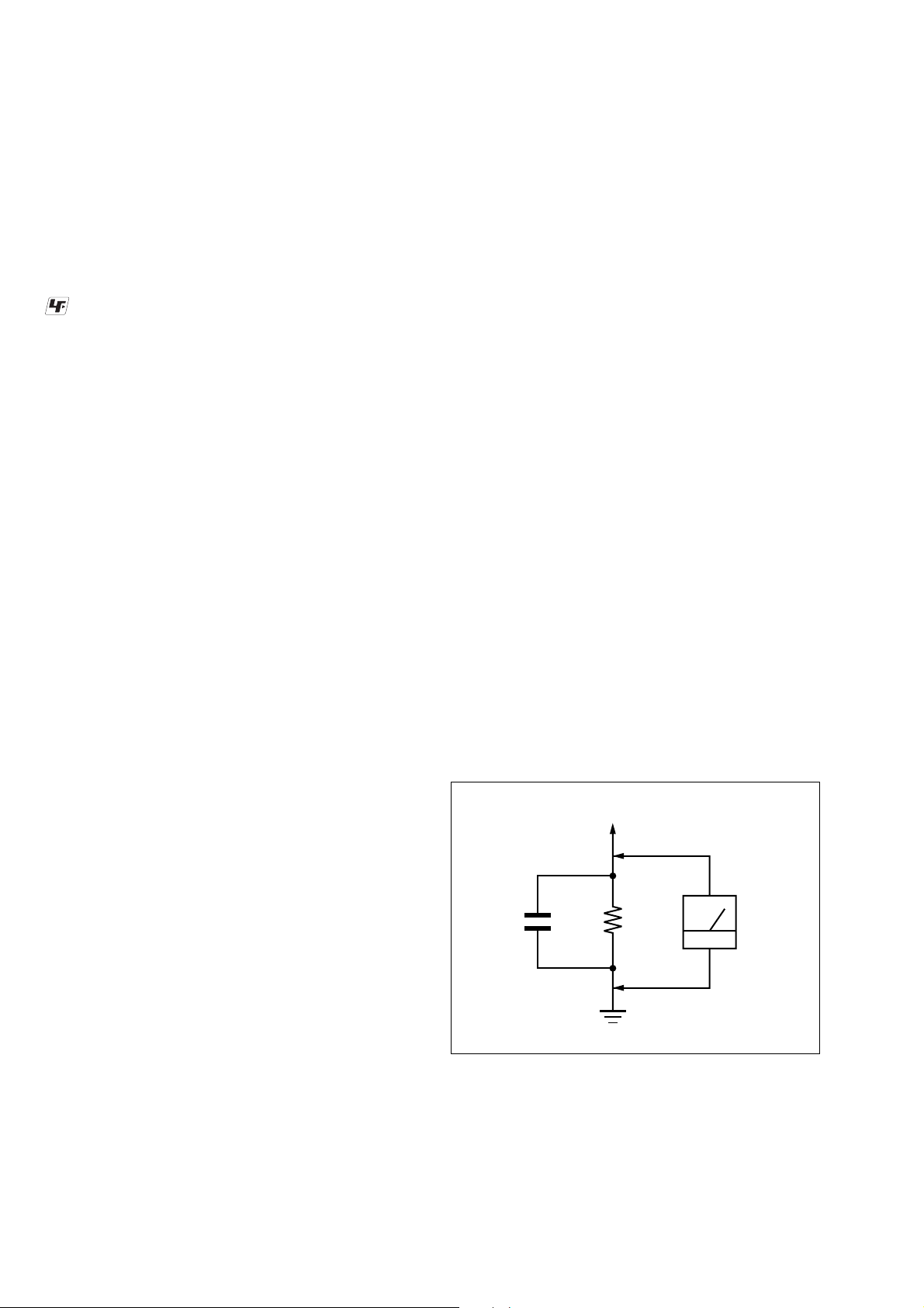
LEAKAGE TEST
The AC leakage from any exposed metal part to earth ground and
from all exposed metal parts to any exposed metal part having a
return to chassis, must not exceed 0.5 mA (500 microamperes.).
Leakage current can be measured by any one of three methods.
1. A commercial leakage tester, such as the Simpson 229 or RCA
WT -540A. Follow the manufactur ers’ instructions to use these
instruments.
2. A battery-operated A C milliammeter . The Data Precision 245
digital multimeter is suitable for this job.
3. Measuring the voltage drop across a resistor by means of a
VOM or battery-operated AC v oltmeter. The “limit” indication
is 0.75 V, so analog meters must have an accurate low-v oltage
scale. The Simpson 250 and Sanwa SH-63Trd are examples
of a passive VOM that is suitable. Nearly all battery operated
digital multimeters that have a 2 V A C range are suitable. (See
Fig. A)
To Exposed Metal
Parts on Set
AC
0.15 µF
1.5 k
Ω
Earth Ground
voltmeter
(0.75 V)
Fig. A. Using an AC voltmeter to check AC leakage.
SAFETY-RELATED COMPONENT WARNING!!
COMPONENTS IDENTIFIED BY MARK 0 OR DOTTED LINE
WITH MARK 0 ON THE SCHEMATIC DIAGRAMS AND IN
THE PARTS LIST ARE CRITICAL TO SAFE OPERATION.
REPLACE THESE COMPONENTS WITH SONY PAR TS WHOSE
PART NUMBERS APPEAR AS SHOWN IN THIS MANU AL OR
IN SUPPLEMENTS PUBLISHED BY SONY.
2
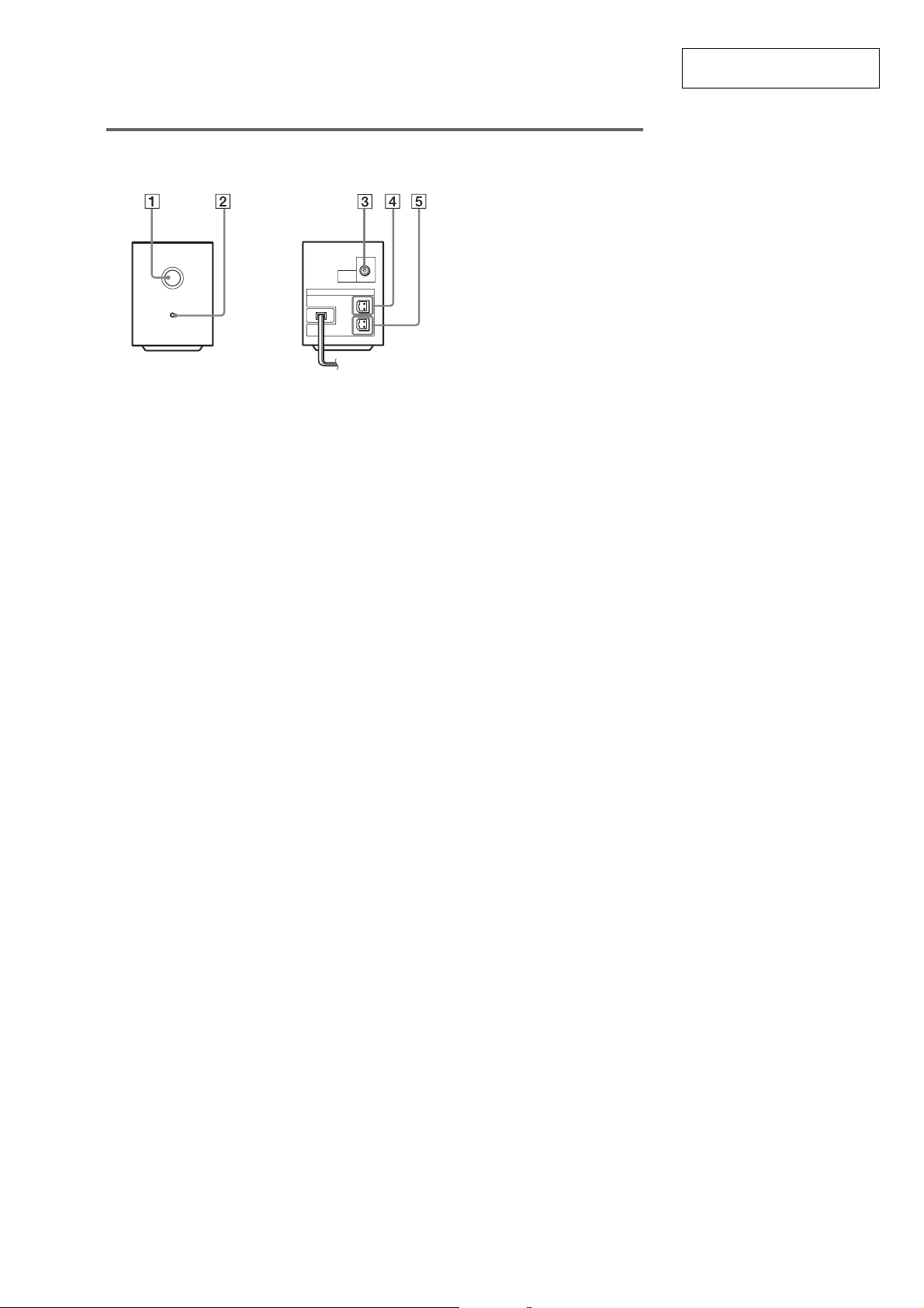
LOCATION OF CONTROLS
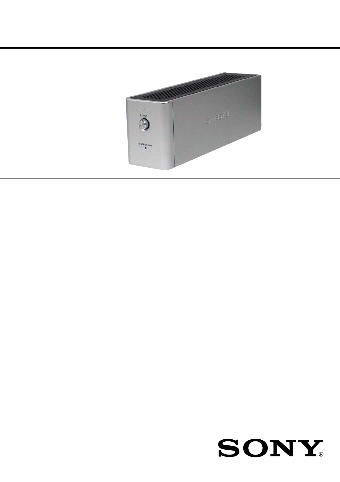
Surround amplifier
SECTION 1
GENERAL
TA-SB500WR2
This section is extracted from
instruction manual.
Front panel
POWER
POWER ON-LINE
A POWER (ON/OFF)
B POWER/ON LINE indicator
C DIR-R1 jack
D SURROUND L SPEAKER jack
E SURROUND R SPEAKER jack
Rear panel
DIR-R1
SPEAKER
SURROUND L
SURROUND R
3
TA-SB500WR2
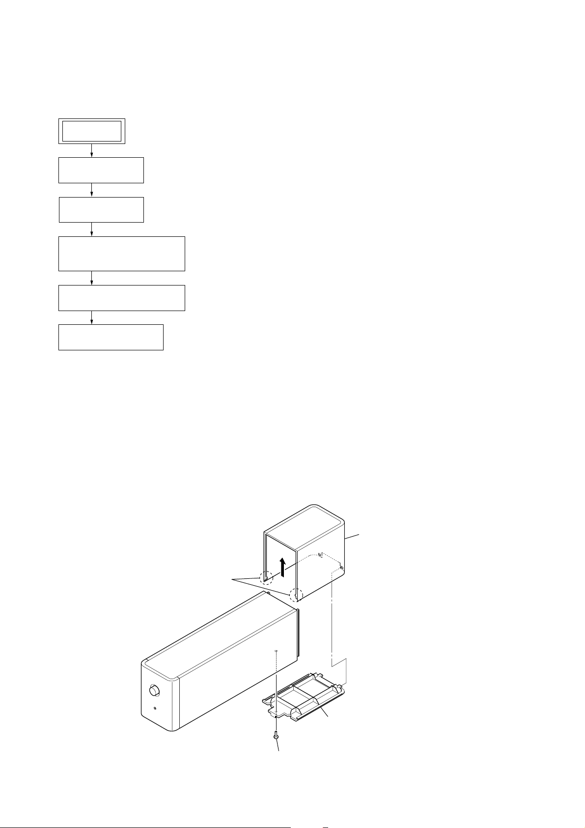
• This set can be disassembled in the order shown below.
2-1. DISASSEMBLY FLOW
SET
2-2. WIRE COVER
(Page 4)
2-3. TOP PANEL
(Page 5)
2-4. SIDE PANEL,
FRONT PANEL BLOCK
(Page 5)
2-5. DIAT POWER BOARD
(Page 6)
SECTION 2
DISASSEMBLY
2-6. DIAT AMP BOARD
(Page 6)
Note: Follow the disassembly procedure in the numerical order given.
2-2. WIRE COVER
3
two claws
4
wire cover
2
wire (A) holder
1
screw (B3 × 8)
4
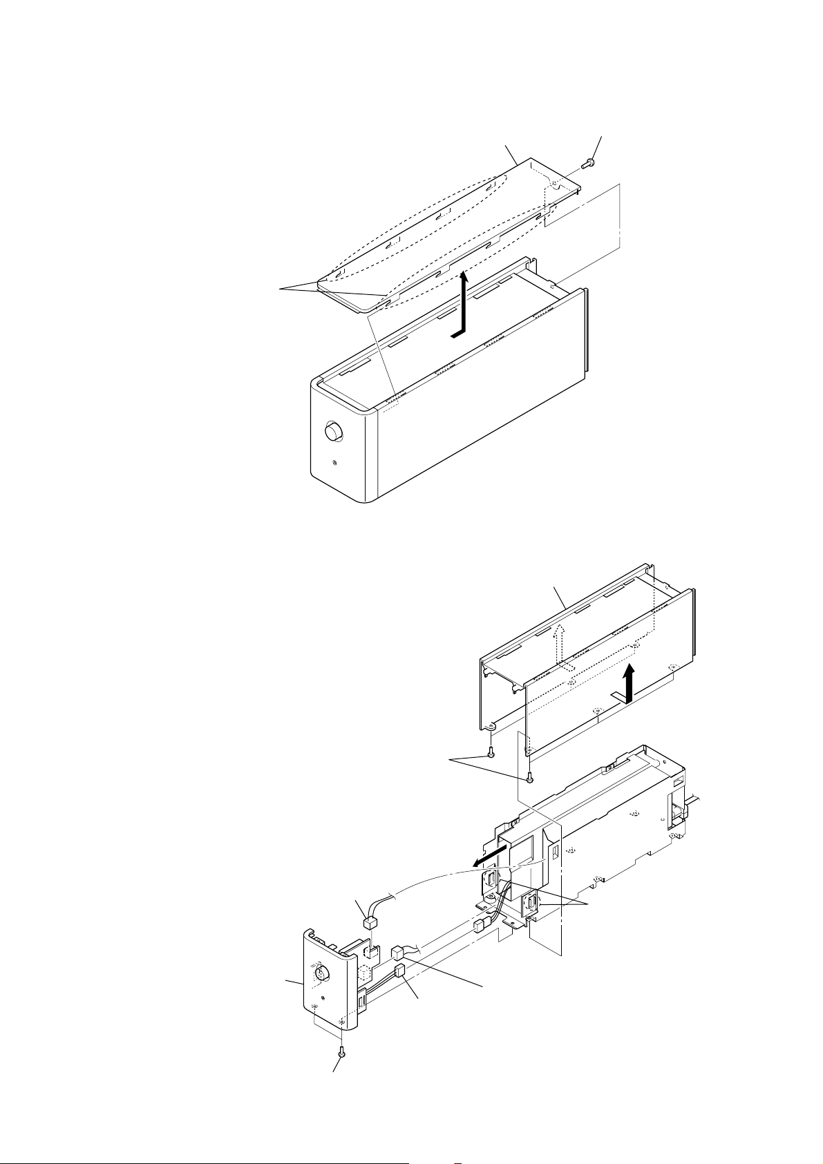
2-3. TOP PANEL
)
3
eight claws
4
top panel
2
1
screw
(BVTP3
TA-SB500WR2
×
10
2-4. SIDE PANEL, FRONT PANEL BLOCK
7
connector
(CN902)
1
six screws
(2.6
3
side panel
2
2
×
6)
6
5
two claws
8
front panel block
4
two screws
(2.6
7
connector
7
connector
×
6)
(CN901)
5
TA-SB500WR2
s
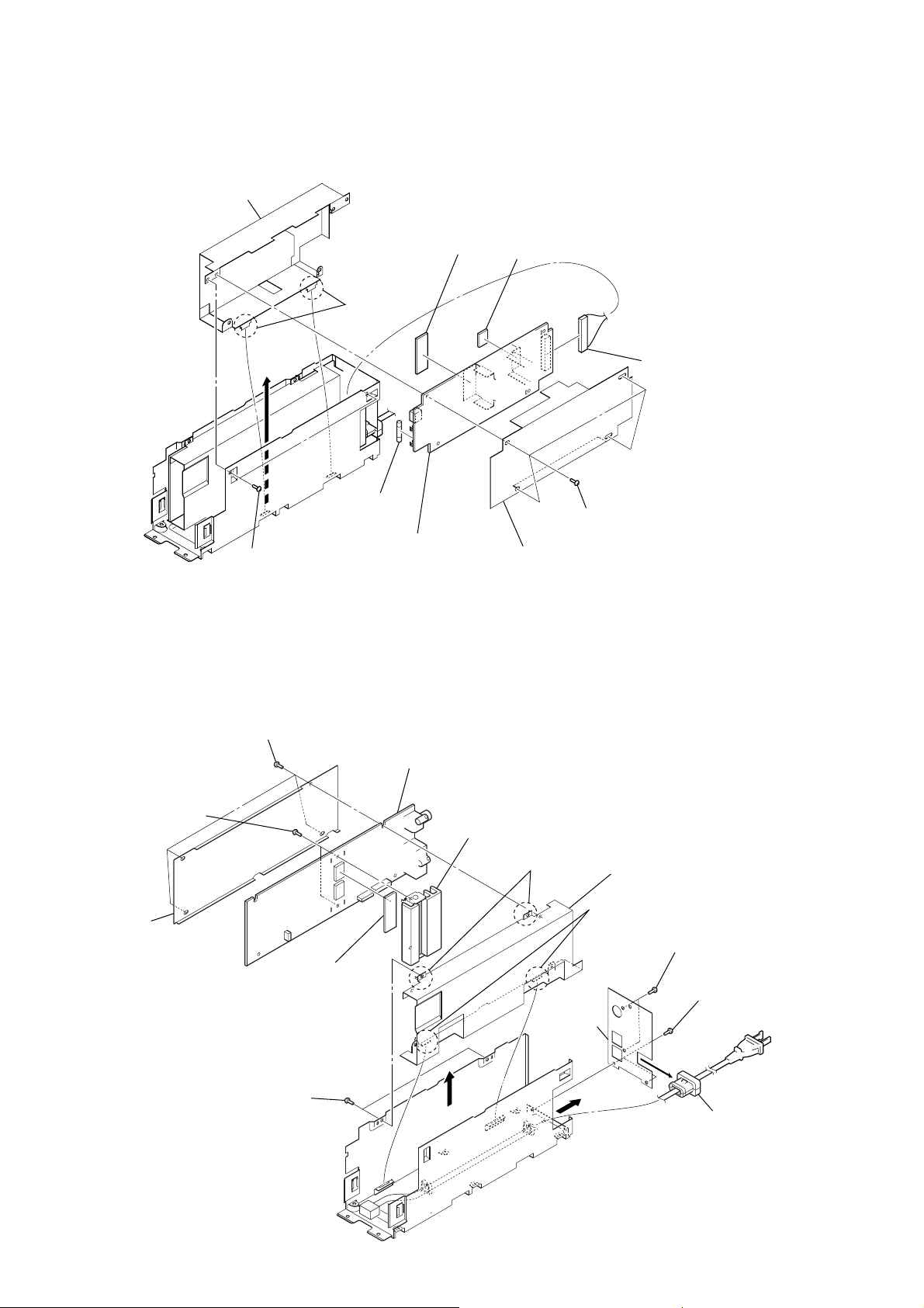
2-5. DIAT POWER BOARD
7
power shield
3
2
two claws
8
radiation sheet
(DMB)
8
radiation sheet
4
two connector
(CN904)
2-6. DIAT AMP BOARD
qd
two screws
qa
sheet AMP
(BVTP3
×
6)
1
0
four screws
(2.6
two screws
(2.6
×
6)
×
6)
qg
radiation sheet
9
fuse (F901)
0
DIAT POWER board
qh
DIAT AMP board
qf
6
A sheet power
heat sink block
7
two claws
5
back
panel
5
four screws
(2.6
qs
8
two claws
×
6)
AMP shield
1
two screws
(BVTP3
2
two screws
(BVTP3
×
8)
×
8)
6
two screws
(2.6
×
6)
9
3
4
cord bushing
6
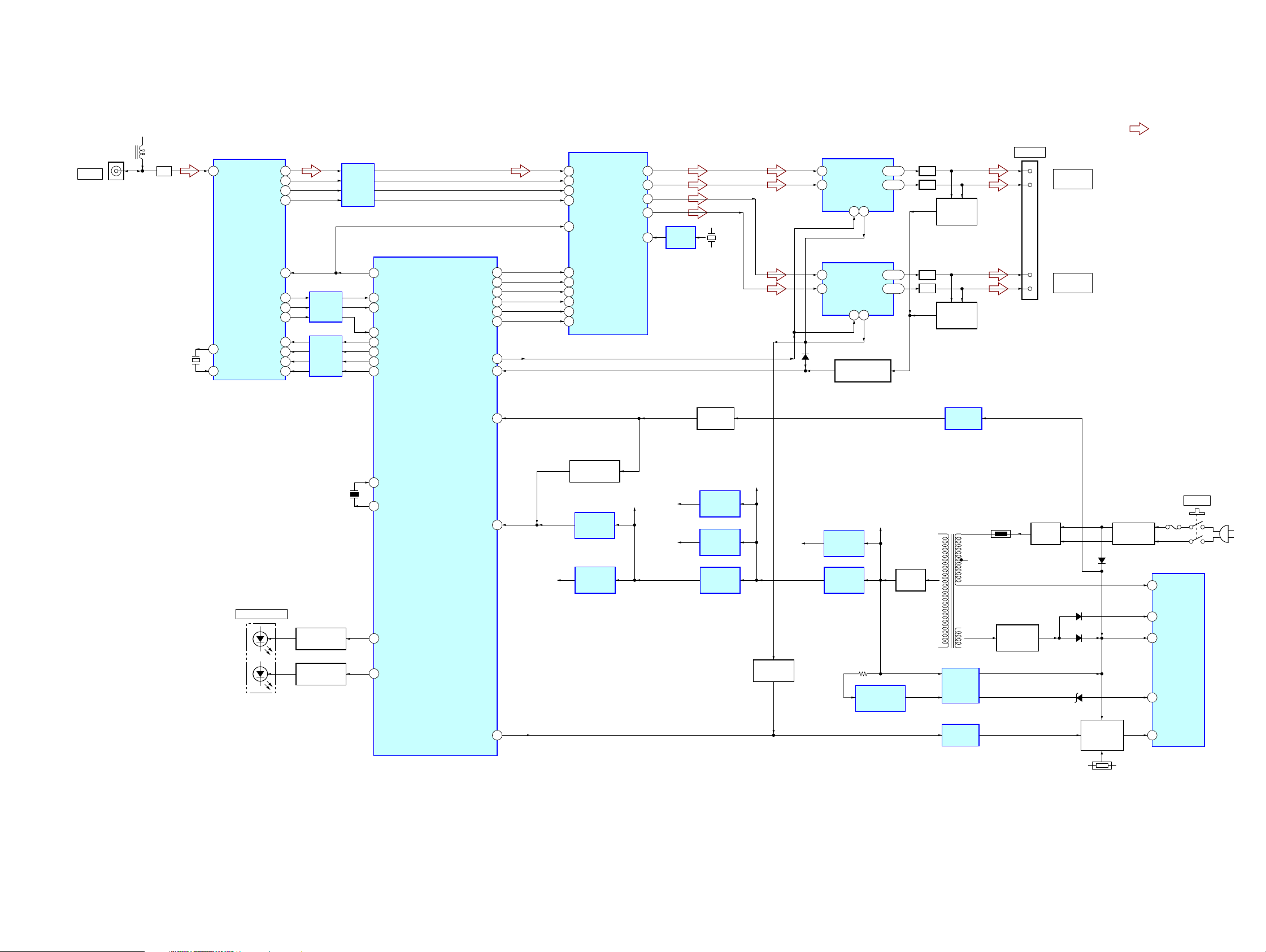
3-1. BLOCK DIAGRAM
VCC2
J301
DIR-R1
LPF
X101
12.288MHz
RF DEMODULATOR,
A/D CONVERTER
10
ADVIN
OSCO
4043OSCI
IC102
DAOUT
BCK
LRCK
APX
/XRST
CSOD
DTVALID
SRDT
SWDT
SCLK
/XSCEN
SCMODE
TA-SB500WR2
SECTION 3
DIAGRAMS
• SIGNAL PATH
IC301
STREAM PROCESSOR
60
54
59
31
13
33
61
34
35
37
36
38
IC106
LEVEL
SHIFT
IC103
LEVEL
SHIFT
IC109
LEVEL
SHIFT
SURROUND AMP CONTROLLER
26 XRST_INIT
15 CSOD
14 DTVALID
53 DIAT_SRDT
52 DIAT_SWDT
51 DIAT_SCLK
50 XSCEN
48 SCMODE
IC107
DAMP_SCDT
DAMP_SHIFT
DAMP_LATCH
DAMP_NSPMUTE
DAMP_SOFTMUTE
DAMP_PGMUTE
DRIVER_RST
DRIVER_OCP
61
60
59
35
34
33
37
38
31
DATA
30
BCK
29
LRCK
36
XFSIIN
27
INIT
21
SCDT
22
SCSHIFT
23
SCLATCH
18
NSPMUTE
19
SOFTMUTE
20
PGMUTE
OUTL1
OUTL2
OUTR1
OUTR2
XFSOIN
11
9
6
4
IC114
48
OSC
X103
49.152MHz
D300
POWER DRIVER
2
PWM_BP
17
PWM_AP
POWER DRIVER
2
PWM_BP
17
PWM_AP
PROTECT DETECT
IC110
/RST
4 13
IC112
/RST
4 13
Q107
OUT_B
OUT_A
/SD
OUT_B
OUT_A
/SD
29, 30
25, 26
29, 30
25, 26
LPF
LPF
LPF
LPF
Q108, 109
OVER LOAD
DETECT
Q105, 106
OVER LOAD
DETECT
TB301
SPEAKER
(+)
(–)
(+)
(–)
SURROUND
L
SURROUND
R
: AUDIO
D400
POWER/ON-LINE
LED DRIVE
Q104, 112
LED DRIVE
Q103, 111
X102
8MHz
22
X0
X1
23
41
LED_GREEN
42
LED_RED
AC CUT
/RESET
MAIN_OFF
17
RESET SWITCH
Q102
+3.3V
+1.5V
19
+1.8V
57
VOLTAGE
DETECT
IC105
+1.8V
REGULATOR
IC113
+2.5V
AC CUT
Q110
+1.5V
REGULATOR
IC101
+2.5V
REGULATOR
IC104
+3.3V
REGULATOR
IC108
VCC2
PROTECTOR
Q300
+12V
+12V
REGULATOR
IC903
DC/DC
CONVERTER
IC904
+27.5V
SHUNT
REGULATOR
IC905
RECT
D921
ISOLATOR
PC902
POWER
TRANSFORMER
T901
ISOLATOR
PC901
ISOLATOR
PC903
TH901
REGULATOR
Q901
RECT
D901
D907, 909
D908
D910
D911
OVER LOAD
PROTECT
Q902, 903
TH902
LINE FILTER
POWER
F901
1
D
7
OCP/BD
4
VCC
6
FB
5
OLP/SS
POWER CONTROL
IC901
S901
(AC IN)
TA-SB500WR2
77
TA-SB500WR2
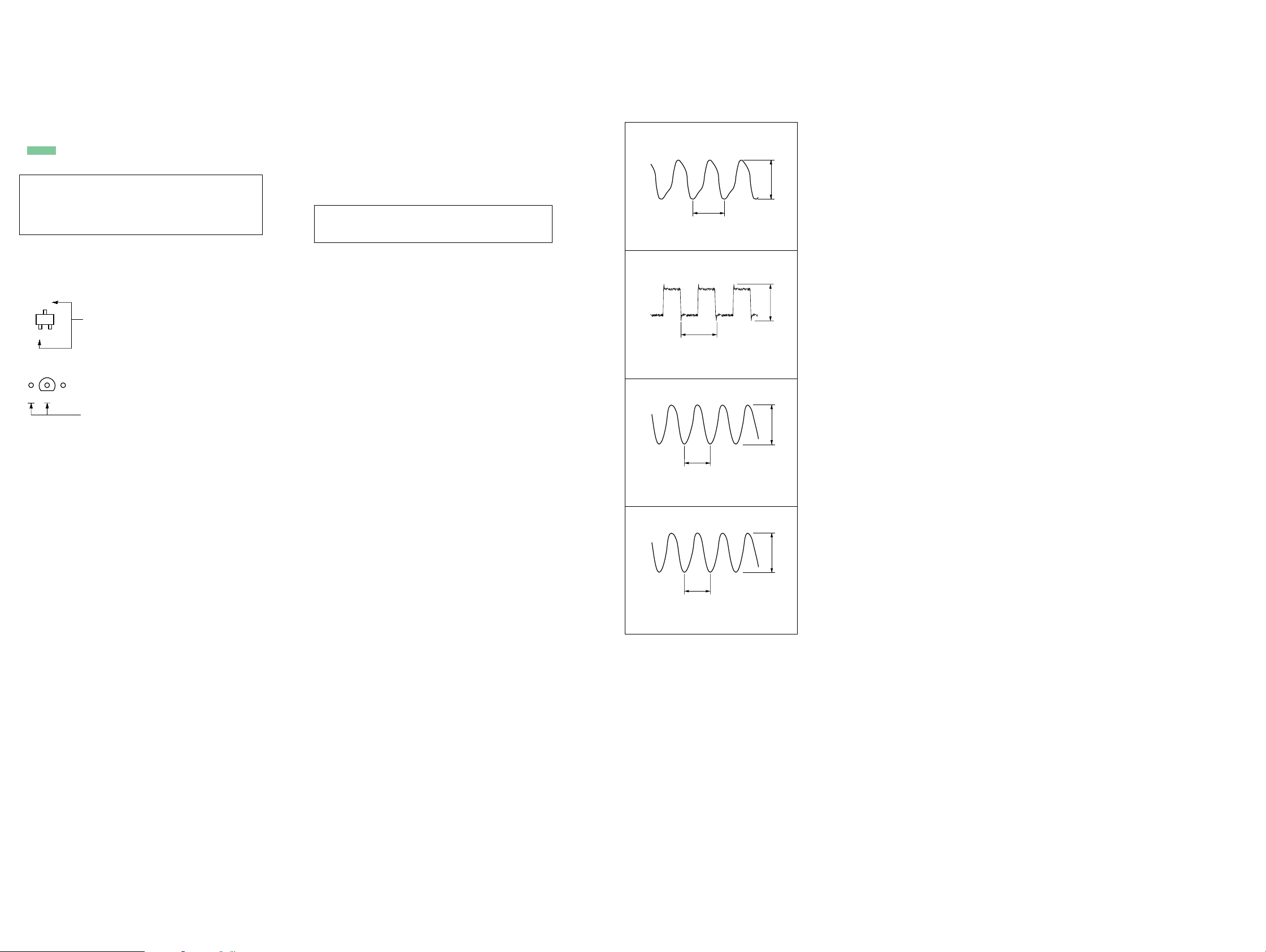
20.3 ns
3.4 Vp-p
125 ns
3.4 Vp-p
325 ns
3.2 Vp-p
82 ns
2.9 Vp-p
• Note for Printed Wiring Boards and Schematic Diagrams
Note on Printed Wiring Boards:
• X : parts extracted from the component side.
• Y : parts extracted from the conductor side.
f
•
• : Pattern from the side which enables seeing.
(The other layers' patterns are not indicated.)
Caution:
Pattern face side: Parts on the pattern face side seen from
(Conductor Side) the pattern face are indicated.
Parts face side: Parts on the parts face side seen from
(Component Side) the parts face are indicated.
• DIAT AMP board is multi-layer printed board.
• Indication of transistor.
: internal component.
However, the patter ns of intermediate layers have not been
included in diagrams.
C
B
Q
B
E
Q
CE
These are omitted.
These are omitted.
Note on Schematic Diagram:
• All capacitors are in µF unless otherwise noted. (p: pF)
50 WV or less are not indicated except for electrolytics
and tantalums.
• All resistors are in Ω and
specified.
•
f : internal component.
• 2 : nonflammable resistor.
• C : panel designation.
Note: The components identified by mark 0 or dotted line
with mark 0 are critical for safety.
Replace only with part number specified.
• A : B+ Line.
• Voltages and waveforms are dc with respect to ground
under no-signal (detuned) conditions.
Note: When mesurering voltages and waveforms, con-
nect with HCD-SB500W (HCD-SB500W states:
DVD play).
no mark : DVD PLAY
∗ : Impossible to measure
• Voltages are taken with a VOM (Input impedance 10 MΩ).
Voltage variations may be noted due to normal production tolerances.
• Waveforms are taken with a oscilloscope.
Voltage variations may be noted due to normal production tolerances.
• Circled numbers refer to waveforms.
• Signal path.
F : AUDIO
1
4
/
W or less unless otherwise
• Waveforms
– DIAT AMP Board –
IC102 rd (OSCO)
1
1 V/DIV, 50 ns/DIV
IC102 tf (BCK)
2
1 V/DIV, 200 ns/DIV
IC107 wd (X1)
3
4
1 V/DIV, 50 ns/DIV
IC114 4
2 V/DIV, 10 ns/DIV
TA-SB500WR2
88
TA-SB500WR2
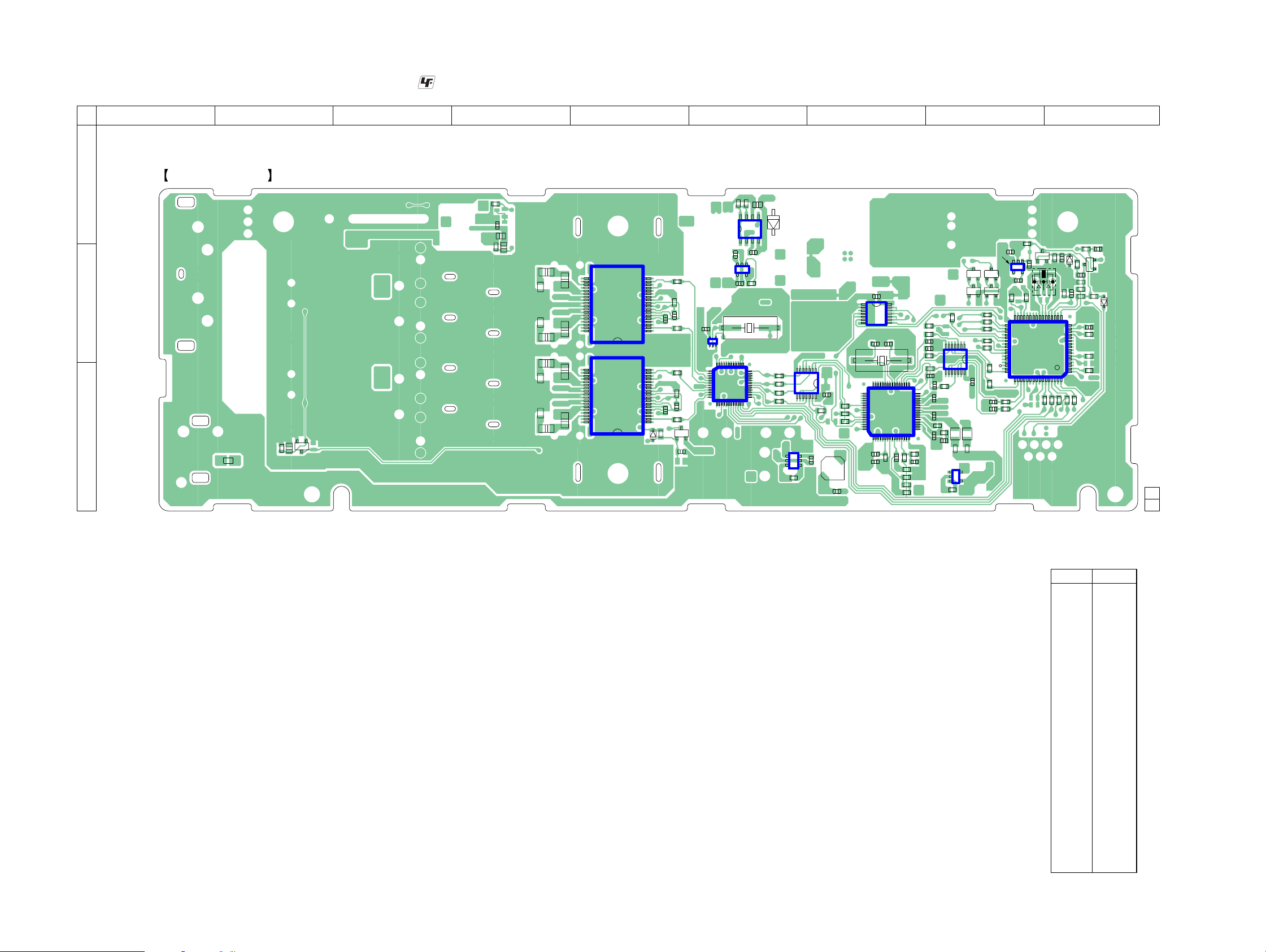
3-2. PRINTED WIRING BOARD – DIAT AMP Section (1/2) –
1 2 3 4 5 6 7 8 9
DIAT AMP BOARD
(COMPONENT SIDE)
A
B
C
R155
FB109
C166
Q107
E
B
C
: Uses unleaded solder.
R950
C938
C937
R952
C954
C222
R198
R189
C208
C191
R180
R167
C181
C221
C207
C190
C180
R940
14
1
3
54
R199
C223
X103
3748
36
25
24
C951
58
C940
IC113
R162
R163
R161
R160
D922
IC109
7
8
IC104
3
1
R117
R168
4
6
1
14
C142
IC106
C167
R119
R118
R120
L101
C105
1
7
49
64
C131
C132
C129
X101
C149
IC102
1
C120
R116
C124
R111
R111
R111
R264
R265
R140
R124
X102
R131
17
64
R137
C147
R134
D102
C266
16
1
R138
R259
R123
C
R130
E
B
C143
C143
C143
R171
R171
R171
R152
R152
R152
R133
R129
C253
Q110
D103
C156
R283
R258
R127
1-872-329-
11
(11)
Q102
C
EBE
C
EBE
R149
R151
L103
Q103
Q103
Q103
C
C
R141
R122
C145
R252
33
48
R145
IC105
Q112 Q111
B
B
14
8
R261
R115
C123
C126
R114
R112
C122
3348
C125
32
C108
17
C111
16
R110
R109
C116
R266
R262
IC103
7
8
R113
C113
R104
L102
R102
C110
FB101
135
R101
Q104
R146
R147
R148
R150
1
C133
14
C159
FB102
IC101
4
C158
C146
13
54
R253
32
IC107
49
R144
C148
C
E
B
R941
IC904
C234
R183
D300
18
1
18
1
C244
C243
R300
R196
C211
R181
IC114
R175
R178
C186
R173
C
BE
Q300
C300
C233
5
1
12
4
13
13
IC301
19
IC112
36
19
IC110
36
• Semiconductor
Location
Ref. No. Location
D102 B-9
D103 B-9
D300 C-5
D922 A-6
IC101 C-8
IC102 C-7
IC103 B-8
IC104 C-6
IC105 B-8
IC106 B-7
IC107 B-8
IC109 C-6
IC110 C-5
IC112 B-5
IC113 B-6
IC114 B-6
IC301 C-6
IC904 A-6
Q102 A-8
Q103 B-8
Q104 B-8
Q107 C-2
Q110 B-9
Q111 B-8
Q112 B-8
Q300 C-5
TA-SB500WR2
99
 Loading...