Sony TA-SB500WR Service Manual
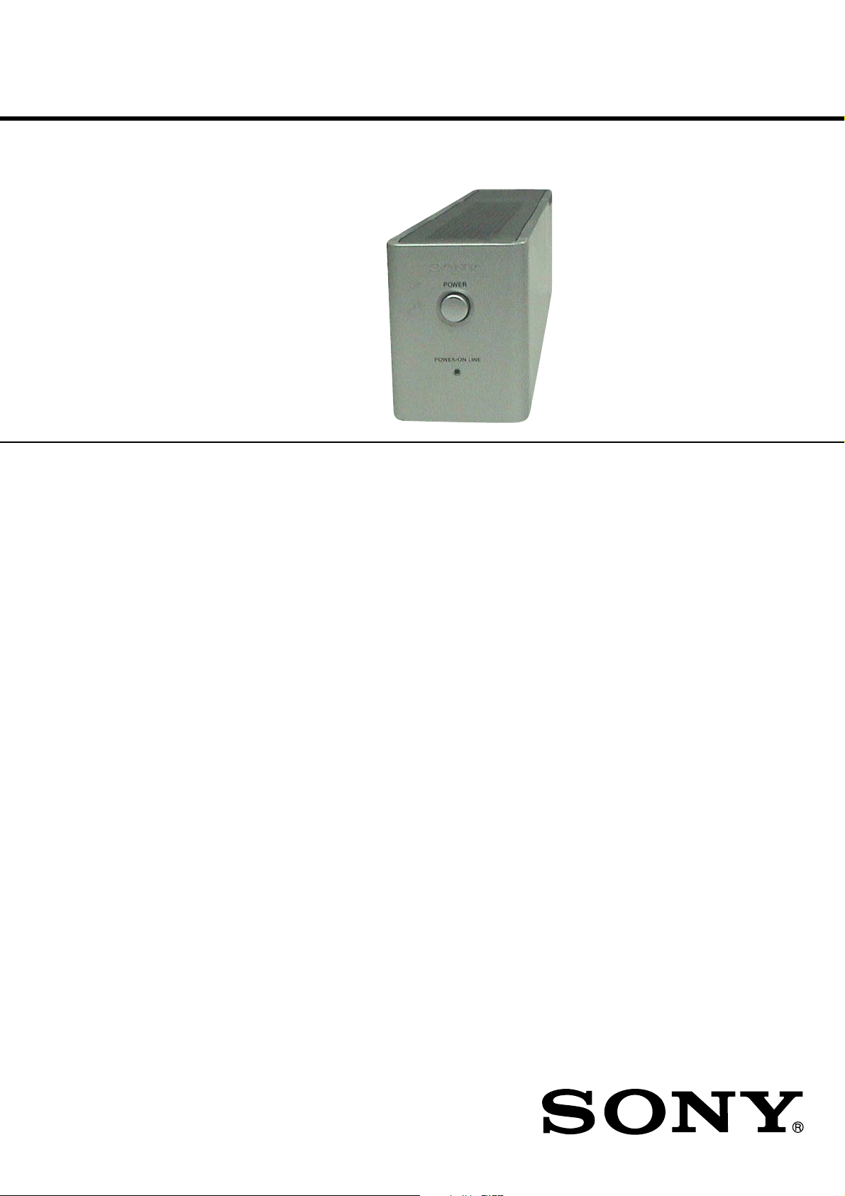
TA-SB500WR
SERVICE MANUAL
Ver. 1.2 2007.07
• T A-SB500WR is the amplifier section in D A V -DZ531W/
LF10/SB500W/WAHT-SD1.
• Refer to the supplement-1 of this service manual for
TA-SB500WR in DAV-DZ531W/WAHT-SD1.
SPECIFICATIONS
AUDIO POWER SPECIFICATIONS
for the US model
POWER OUTPUT AND
TOTAL HARMONIC
DISTORTION: With 4 ohm loads, both
Amplifier section
Stereo mode (rated) 86 W + 86 W (4 ohms at
Surround mode (reference) music power output
channels driven, from
200 – 20,000 Hz; rated
65 watts per channel
minimum RMS power,
with no more than 0.7 %
total harmonic distortion
from 250 milli watts to
rated output.
1 kHz, THD 10 %)
for DAV-LF10:
(with SS-TSL11)
for DAV-SB500W: 96 W + 96 W*
(with SS-TS11)
86 W*
US Model
Canadian Model
AEP Model
UK Model
E Model
Australian Model
Surround amplifier
Power requirements
North American models: 120 V AC, 60 Hz
Taiwan model: 120 V AC, 50/60 Hz
Other models: 220-240 V AC, 50/60 Hz
Power consumption 36 W (120 V AC)
36 W (220-240 V AC)
Dimensions (approx.) 65 × 90 × 335 mm
(2 5/8 × 3 5/8 × 13 1/4
inches) (w/h/d) incl.
speaker cord cover
Mass (approx.) 1.3 kg (2 lb 14 oz)
Design and specifications are subject to change
without notice.
9-879-016-03
2007G05-1
© 2007.07
* Depending on the sound field settings and the source,
there may be no sound output.
SURROUND AMPLIFIER
Sony Corporation
Home Audio Division
Published by Sony Techno Create Corporation
TA-SB500WR
r
Notes on chip component replacement
• Never reuse a disconnected chip component.
• Notice that the minus side of a tantalum capacitor may be
damaged by heat.
UNLEADED SOLDER
Boards requiring use of unleaded solder are printed with the leadfree mark (LF) indicating the solder contains no lead.
(Caution: Some printed circuit boards may not come printed with
the lead free mark due to their particular size)
: LEAD FREE MARK
Unleaded solder has the following characteristics.
• Unleaded solder melts at a temperature about 40 °C higher
than ordinary solder.
Ordinary soldering irons can be used but the iron tip has to be
applied to the solder joint for a slightly longer time.
Soldering irons using a temperature regulator should be set to
about 350 °C.
Caution: The printed pattern (copper foil) may peel away if
the heated tip is applied for too long, so be careful!
• Strong viscosity
Unleaded solder is more viscou-s (sticky, less prone to flow)
than ordinary solder so use caution not to let solder bridges
occur such as on IC pins, etc.
• Usable with ordinary solder
It is best to use only unleaded solder but unleaded solder may
also be added to ordinary solder.
TABLE OF CONTENTS
1. GENERAL ................................................................... 3
2. DISASSEMBLY
2-1. Disassembly Flow ........................................................... 4
2-2. Wire Cover ...................................................................... 4
2-3. Top Panel ......................................................................... 5
2-4. Side Panel, Front Panel Section....................................... 5
2-5. DIAT POWER Board ...................................................... 6
2-6. DIAT AMP Board............................................................ 6
3. DIAGRAMS
3-1. Block Diagram ................................................................ 7
3-2. Schematic Diagram – DIAT AMP Board (1/3) – ........... 9
3-3. Schematic Diagram – DIAT AMP Board (2/3) – ........... 10
3-4. Schematic Diagram – DIAT AMP Board (3/3) – ........... 11
3-5. Printed Wiring Board
– DIAT AMP Board (Component Side) – ....................... 12
3-6. Printed Wiring Board
– DIAT AMP Board (Conductor Side) – ......................... 13
3-7. Printed Wiring Boards – POWER SUPPLY Section – ... 14
3-8. Schematic Diagram – POWER SUPPLY Section – ....... 15
4. EXPLODED VIEWS
4-1. Panel Section ................................................................... 20
4-2. DIAT AMP/DIAT POWER Boards Section .................... 21
5. ELECTRICAL PARTS LIST................................ 22
SAFETY CHECK-OUT
After correcting the original service problem, perform the following
safety check before releasing the set to the customer:
Check the antenna terminals, metal trim, “metallized” knobs, screws,
and all other exposed metal parts for AC leakage.
Check leakage as described below.
LEAKAGE TEST
The AC leakage from any exposed metal part to earth ground and
from all exposed metal parts to any exposed metal part having a
return to chassis, must not exceed 0.5 mA (500 microamperes.).
Leakage current can be measured by any one of three methods.
1. A commercial leakage tester, such as the Simpson 229 or RCA
WT -540A. Follow the manuf acturers’ instructions to use these
instruments.
2. A battery-operated A C milliammeter . The Data Precision 245
digital multimeter is suitable for this job.
3. Measuring the voltage drop across a resistor by means of a
VOM or battery-operated A C voltmeter . The “limit” indication
is 0.75 V, so analog meters must have an accurate low-v oltage
scale. The Simpson 250 and Sanwa SH-63Trd are examples
of a passive VOM that is suitable. Nearly all battery operated
digital multimeters that have a 2 V A C range are suitable. (See
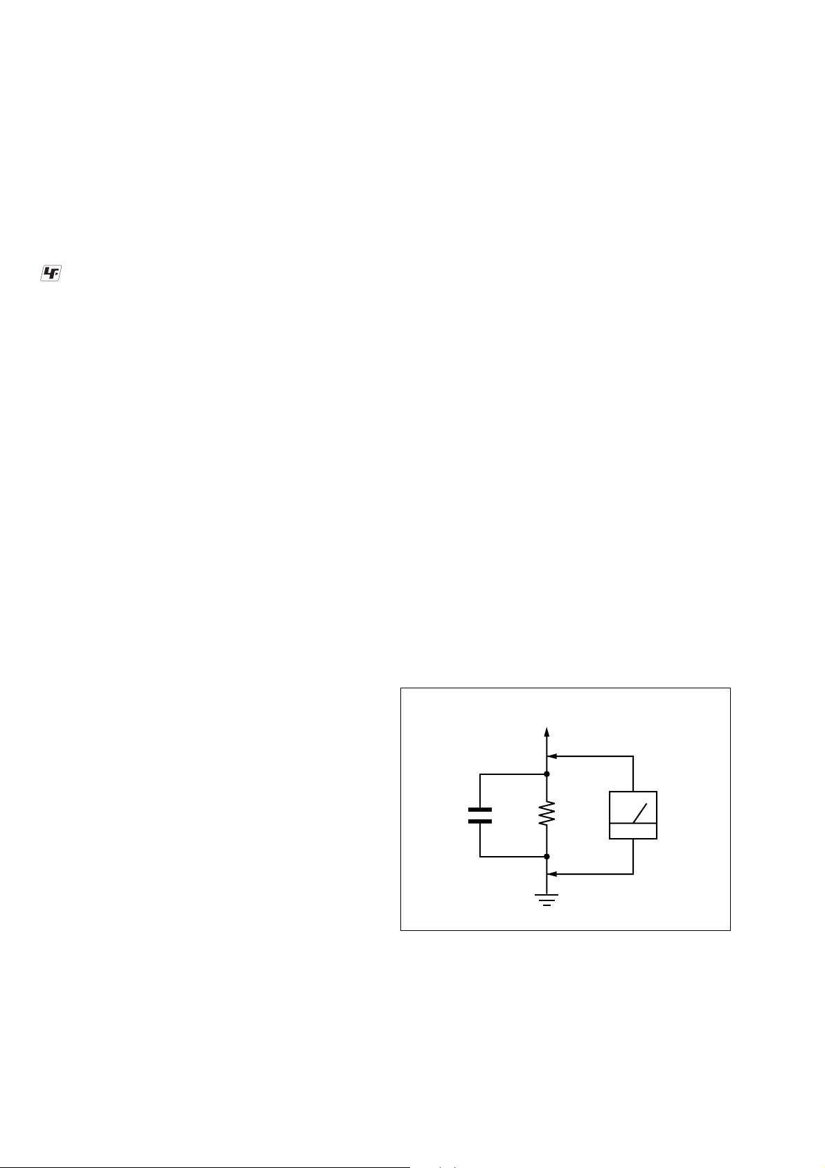
Fig. A)
To Exposed Metal
Parts on Set
AC
0.15 µF
1.5 k
Ω
Earth Ground
voltmete
(0.75 V)
Fig. A. Using an AC voltmeter to check AC leakage.
SAFETY-RELATED COMPONENT WARNING!!
COMPONENTS IDENTIFIED BY MARK 0 OR DOTTED LINE
WITH MARK 0 ON THE SCHEMATIC DIAGRAMS AND IN
THE PARTS LIST ARE CRITICAL TO SAFE OPERATION.
REPLACE THESE COMPONENTS WITH SONY PARTS WHOSE
PART NUMBERS APPEAR AS SHOWN IN THIS MANUAL OR
IN SUPPLEMENTS PUBLISHED BY SONY.
2
ATTENTION AU COMPOSANT AYANT RAPPORT
À LA SÉCURITÉ!
LES COMPOSANTS IDENTIFIÉS P AR UNE MARQUE 0 SUR
LES DIAGRAMMES SCHÉMATIQUES ET LA LISTE DES
PIÈCES SONT CRITIQUES POUR LA SÉCURITÉ DE
FONCTIONNEMENT. NE REMPLACER CES COM- POSANTS
QUE PAR DES PIÈCES SONY DONT LES NUMÉROS SONT
DONNÉS DANS CE MANUEL OU D ANS LES SUPPLÉMENTS
PUBLIÉS PAR SONY.
SECTION 1
GENERAL
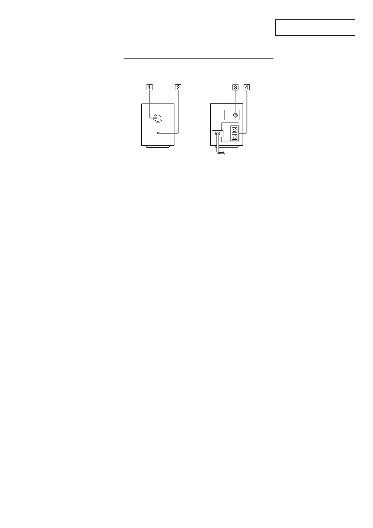
LOCATION OF CONTROLS
Surround amplifier
TA-SB500WR
This section is extracted from
instruction manual.
Front panel
POWER
POWER ON-LINE
A POWER
B POWER/ON LINE indicator
C DIR-R1 jack
D SPEAKER jacks
Rear panel
DIR-R1
SPEAKER
SURROUND
L
SURROUND
R
3
TA-SB500WR
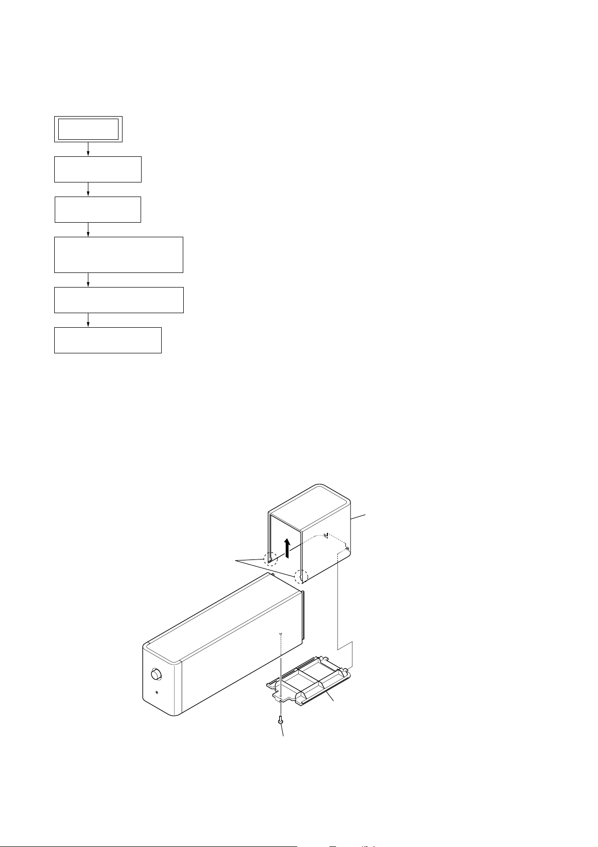
• This set can be disassembled in the order shown below.
2-1. DISASSEMBLY FLOW
SET
2-2. WIRE COVER
(Page 4)
2-3. TOP PANEL
(Page 5)
2-4. SIDE PANEL,
FRONT PANEL SECTION
(Page 5)
2-5. DIAT POWER BOARD
(Page 6)
SECTION 2
DISASSEMBLY
2-6. DIAT AMP BOARD
(Page 6)
Note: Follow the disassembly procedure in the numerical order given.
2-2. WIRE COVER
3
two claws
4
wire cover
2
wire (A) holder
1
screw (B3 × 8)
4
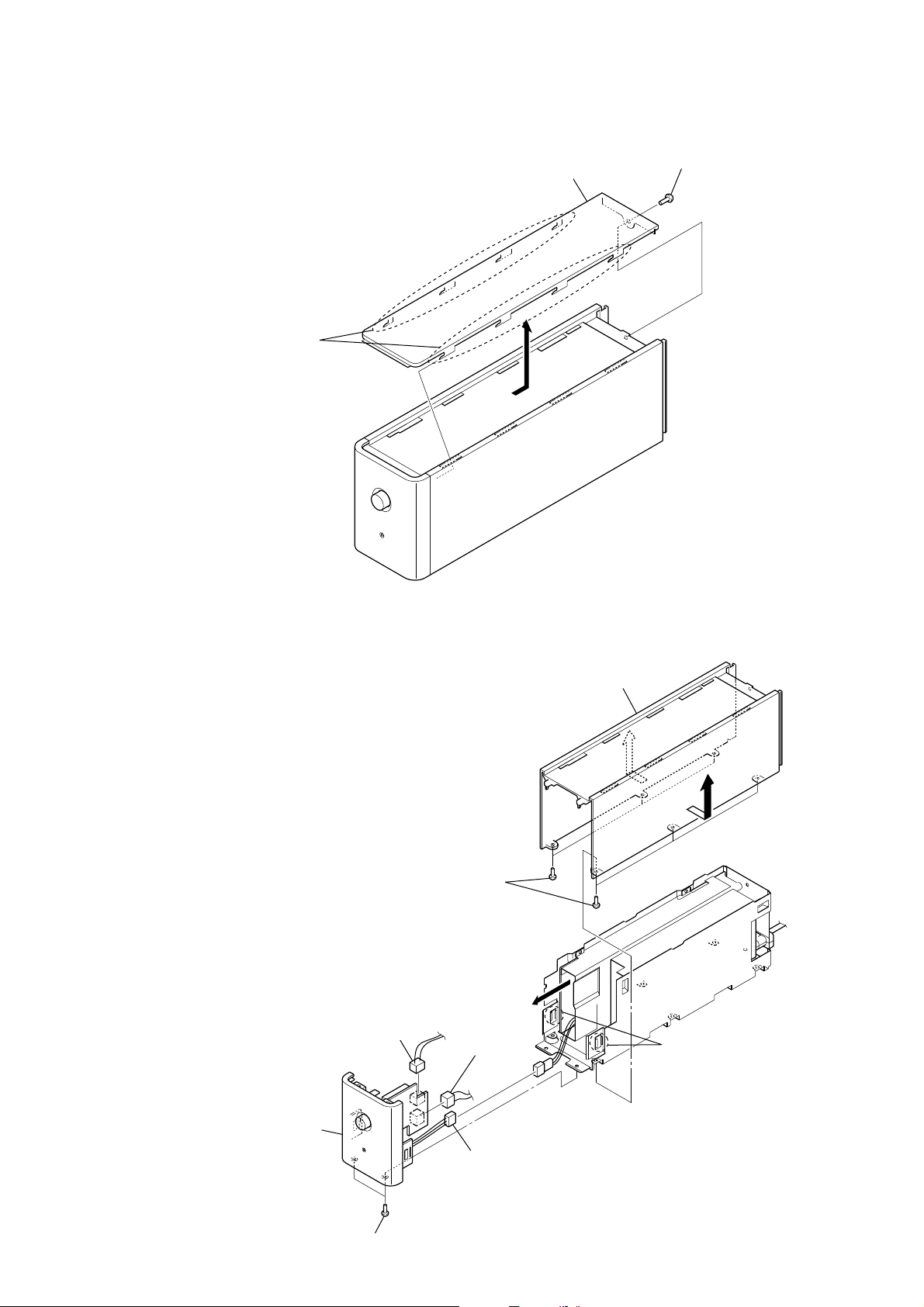
2-3. TOP PANEL
3
eight claws
2
4
top panel
1
screw
(DIA. 2.6)
TA-SB500WR
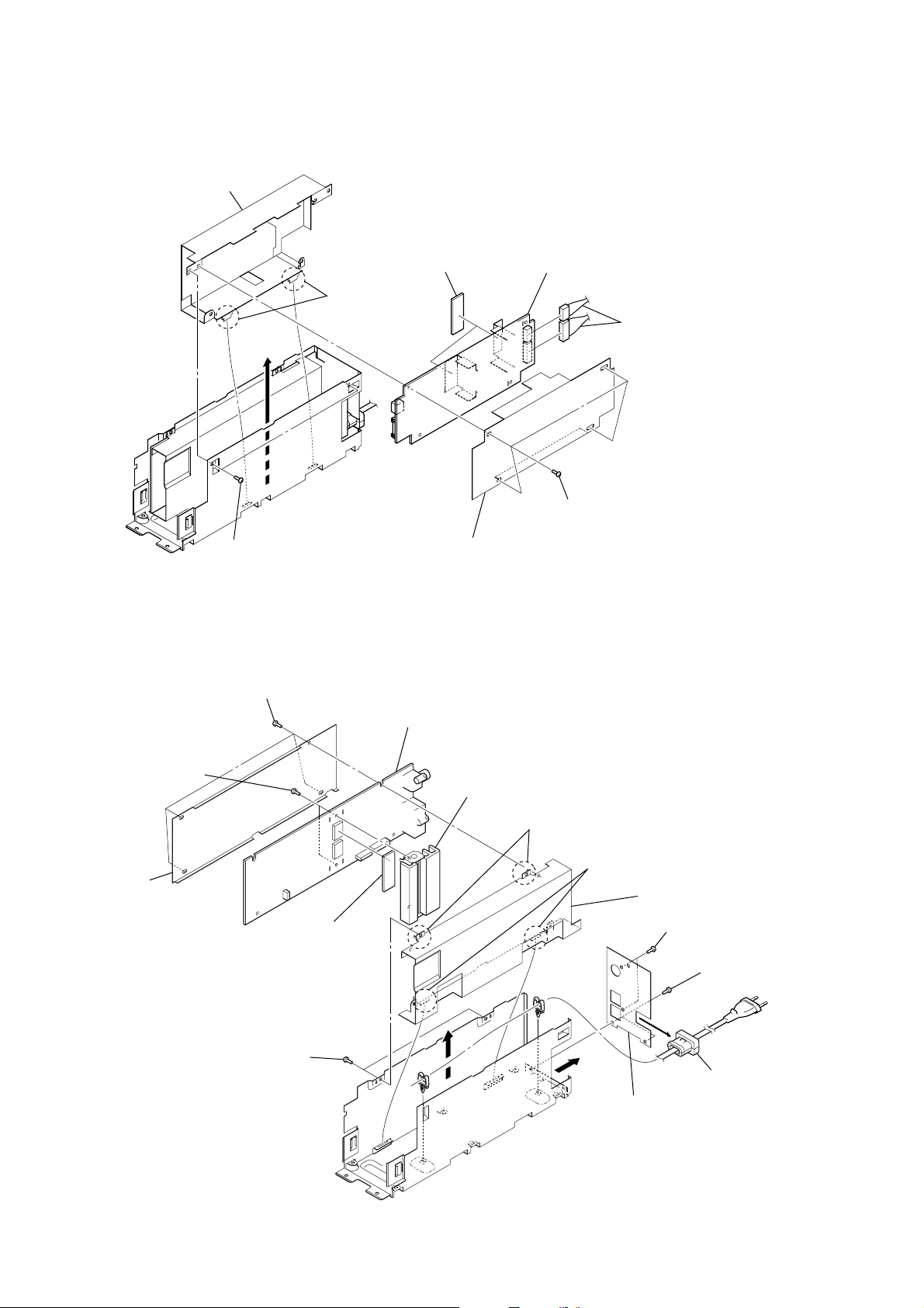
2-4. SIDE PANEL, FRONT PANEL SECTION
1
7
connector
(CN902)
six screws
(DIA. 2.6)
7
connector
(CN901)
6
3
side panel
2
5
two claws
2
8
front panel section
4
two screws
(BVTP3
×
10)
7
connector
5
TA-SB500WR
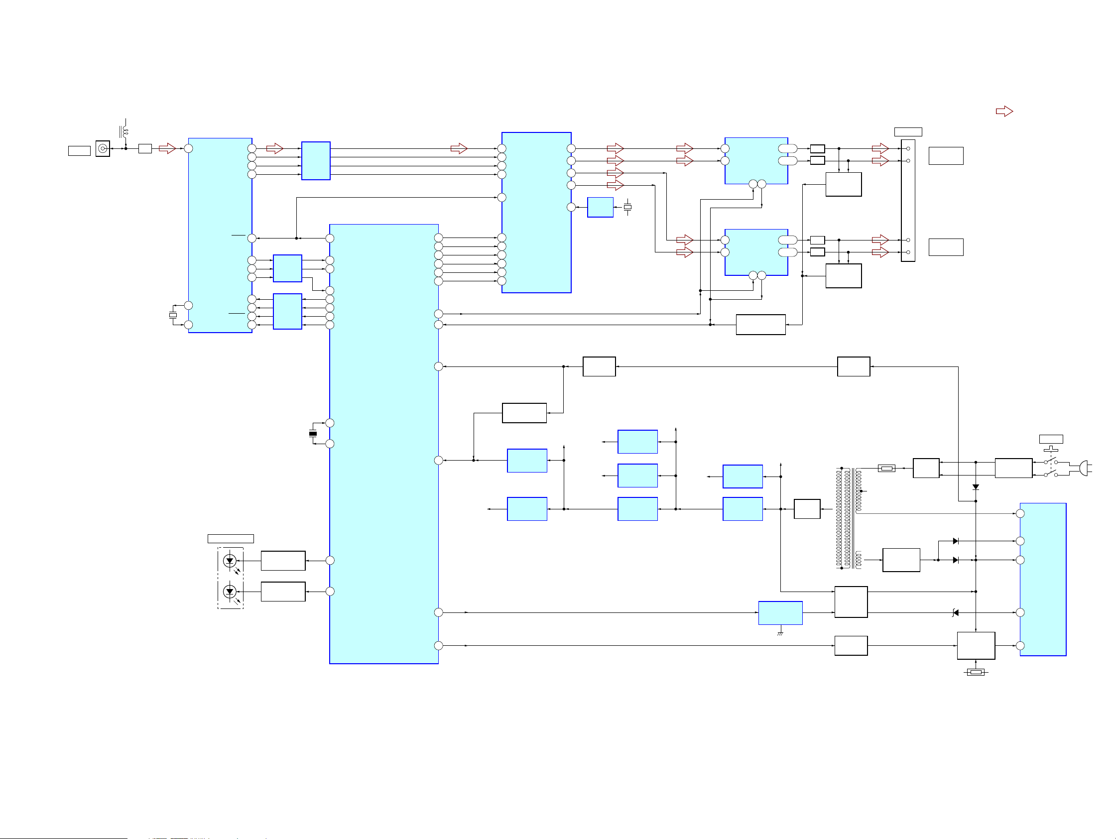
2-5. DIAT POWER BOARD
7
AMP shield
3
2
two claws
8
two radiation sheets
(DMB)
9
DIAT POWER board
4
two connectors
(CN904, CN905)
2-6. DIAT AMP BOARD
qd
two screws
qa
sheet AMP
(BVTP3
×
6)
1
two screws
0
four screws
(DIA. 2.6)
qg
radiation sheet
(AMP)
qh
DIAT AMP board
6
A sheet power
qf
heat sink assy
7
two claws
5
four screws
(DIA. 2.6)
8
two claws
qs
AMP shield
1
two screws
(DIA. 2.6)
2
two screws
(BVTP3
×
10)
6
two screws
(DIA. 2.6)
9
3
5
back panel
4
cord stopper
6
3-1. BLOCK DIAGRAM
IF +5V
J100
DIR-R1
LPF
X101
12.288MHz
RF DEMODULATOR,
A/D CONVERTER
10
ADVIN
OSCO
4043OSCI
IC102
DAOUT
BCK
LRCK
APX
XRST
CSOD
DTVALID
SRDT
SWDT
SCLK
XSCEN
SCMODE
TA-SB500WR
SECTION 3
DIAGRAMS
• SIGNAL PATH
IC111
STREAM PROCESSOR
60
54
59
31
13
33
61
34
35
37
36
38
IC106
LEVEL
SHIFT
IC103
LEVEL
SHIFT
IC109
LEVEL
SHIFT
SURROUND AMP CONTROLLER
26 XRST_INIT
15 CSOD
14 DTVALID
53 DIAT_SRDT
52 DIAT_SWDT
51 DIAT_SCLK
50 XSCEN
48 SCMODE
IC107
DAMP_SCDT
DAMP_SHIFT
DAMP_LATCH
DAMP_NSPMUTE
DAMP_SOFTMUTE
DAMP_PGMUTE
DRIVE_RST
DRIVE_OCP
61
60
59
35
34
33
37
38
31
DATA
30
BCK
29
LRCK
36
XFSIIN
27
INIT
21
SCDT
22
SCSHIFT
23
SCLATCH
18
NSPMUTE
19
SOFTMUTE
20
PGMUTE
OUTL2
OUTL1
OUTR2
OUTR1
XFSOIN
9
11
4
6
IC114
48
OSC
X103
49.152MHz
POWER DRIVER
17
PWM_AP
2
PWM_BP
POWER DRIVER
17
PWM_AP
2
PWM_BP
PROTECT DETECT
IC110
/RST
4 13
IC112
/RST
4 13
Q107
OUT_A
OUT_B
/SD
OUT_A
OUT_B
/SD
25, 26
29, 30
25, 26
29, 30
LPF
LPF
LPF
LPF
Q108, 109
OVER LOAD
DETECT
Q105, 106
OVER LOAD
DETECT
T100
SPEAKER
(+)
(–)
(+)
(–)
SURROUND
L
SURROUND
R
: AUDIO
D400
POWER/ON-LINE
LED DRIVE
Q104, 112
LED DRIVE
Q103, 111
X102
8MHz
22
X0
X1
23
41
LED_GREEN
42
LED_RED
AC CUT
/RESET
V_CONT
MAIN_OFF
17
RESET SWITCH
Q102
+3.3V
19
+1.8V
58
57
VOLTAGE
DETECT
IC105
+1.8V
REGULATOR
IC113
AC CUT
+1.5V
+2.5V
Q110
+1.5V
REGULATOR
IC101
+2.5V
REGULATOR
IC104
+3.3V
REGULATOR
IC108
IF +5V
+12V
+12V
REGULATOR
IC903
DC/DC
CONVERTER
IC904
+30V
SHUNT
REGULATOR
IC905
RECT
D921
ISOLATOR
PC902
POWER
TRANSFORMER
T901
ISOLATOR
PC901
ISOLATOR
PC903
TH901
REGULATOR
+20V
Q901
RECT
D901
D907, 909
D908
D910
D911
OVER LOAD
PROTECT
Q902, 903
TH902
LINE FILTER
LF901, 902
1
7
4
6
5
S901
POWER
D
OCP/BD
VCC
FB
OLP/SS
POWER CONTROL
IC901
(AC IN)
TA-SB500WR
77
TA-SB500WR
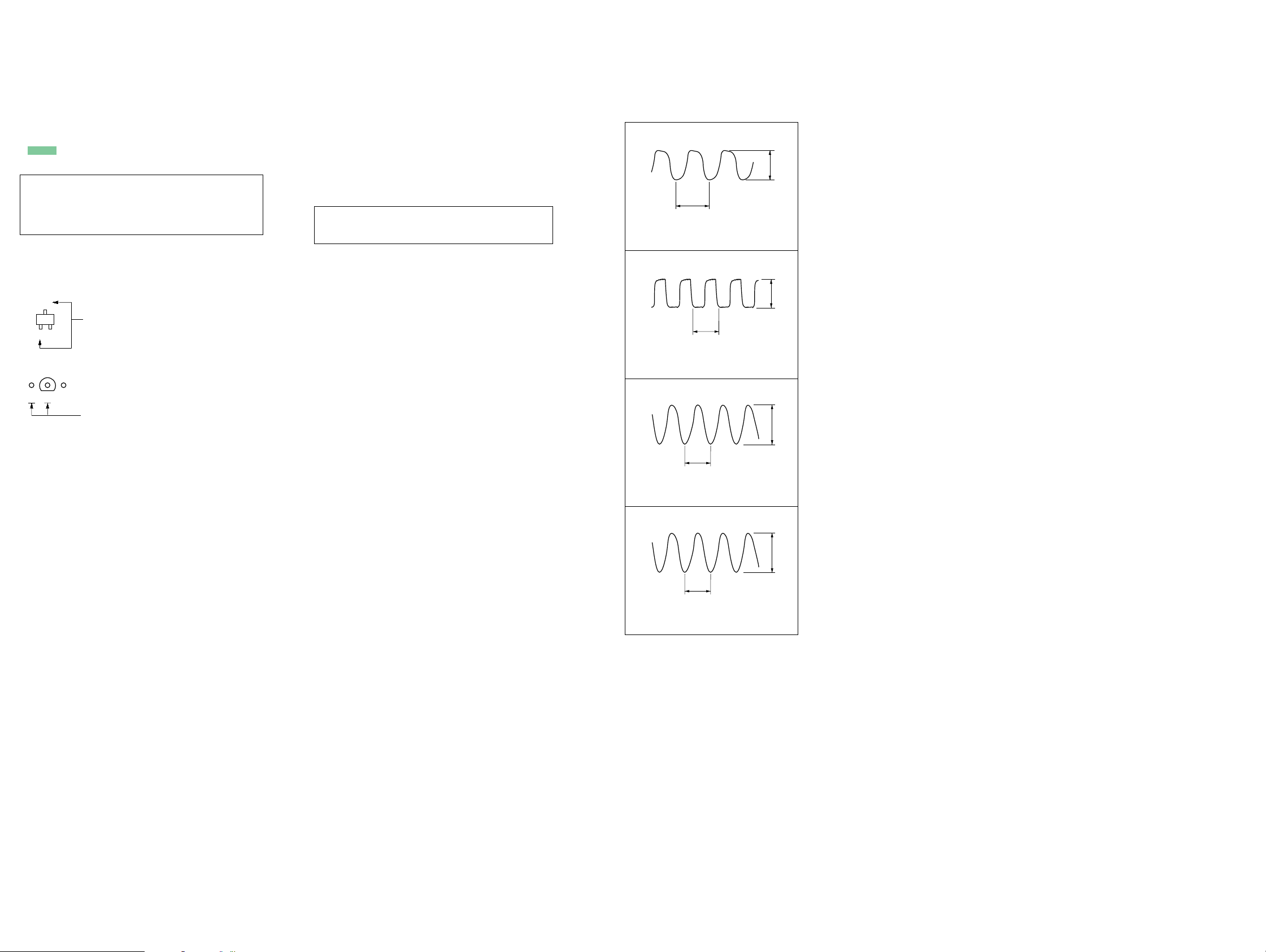
20.3 ns
4.5 Vp-p
125 ns
3.5 Vp-p
325 ns
2.5 Vp-p
81.3 ns
2.5 Vp-p
• Note for Printed Wiring Boards and Schematic Diagrams
Note on Printed Wiring Boards:
• X : parts extracted from the component side.
• Y : parts extracted from the conductor side.
f
•
• : Pattern from the side which enables seeing.
(The other layers' patterns are not indicated.)
Caution:
Pattern face side: Parts on the pattern face side seen from
(Conductor Side) the pattern face are indicated.
Parts face side: Parts on the parts face side seen from
(Component Side) the parts face are indicated.
• DIAT AMP board is multi-layer printed board.
• Indication of transistor.
: internal component.
However, the patter ns of intermediate layers have not been
included in diagrams.
C
B
Q
B
E
Q
CE
These are omitted.
These are omitted.
Note on Schematic Diagram:
• All capacitors are in µF unless otherwise noted. (p: pF)
50 WV or less are not indicated except for electrolytics
and tantalums.
• All resistors are in Ω and 1/
specified.
f : internal component.
•
• 2 : nonflammable resistor.
• C : panel designation.
Note: The components identified by mark 0 or dotted line
with mark 0 are critical for safety.
Replace only with part number specified.
• A : B+ Line.
• Voltages and waveforms are dc with respect to ground
under no-signal (detuned) conditions.
Note: When mesurering voltages and waveforms, con-
nect with HCD-SB500W (HCD-SB500W states:
DVD play).
no mark : DVD PLAY
∗ : Impossible to measure
• Voltages are tak en with a V OM (Input impedance 10 MΩ).
Voltage variations may be noted due to normal production tolerances.
• Waveforms are taken with a oscilloscope.
Voltage variations may be noted due to normal production tolerances.
• Circled numbers refer to waveforms.
• Signal path.
F : AUDIO
• Abbreviation
TW : Taiwan model
4
W or less unless otherwise
• Waveforms
– DIAT AMP Board –
IC102 rd (OSCO)
1
1 V/DIV, 50 ns/DIV
IC102 tf (BCK)
2
1 V/DIV, 100 ns/DIV
IC107 wd (X1)
3
4
1 V/DIV, 50 ns/DIV
IC114 4
2 V/DIV, 10 ns/DIV
TA-SB500WR
88
TA-SB500WR
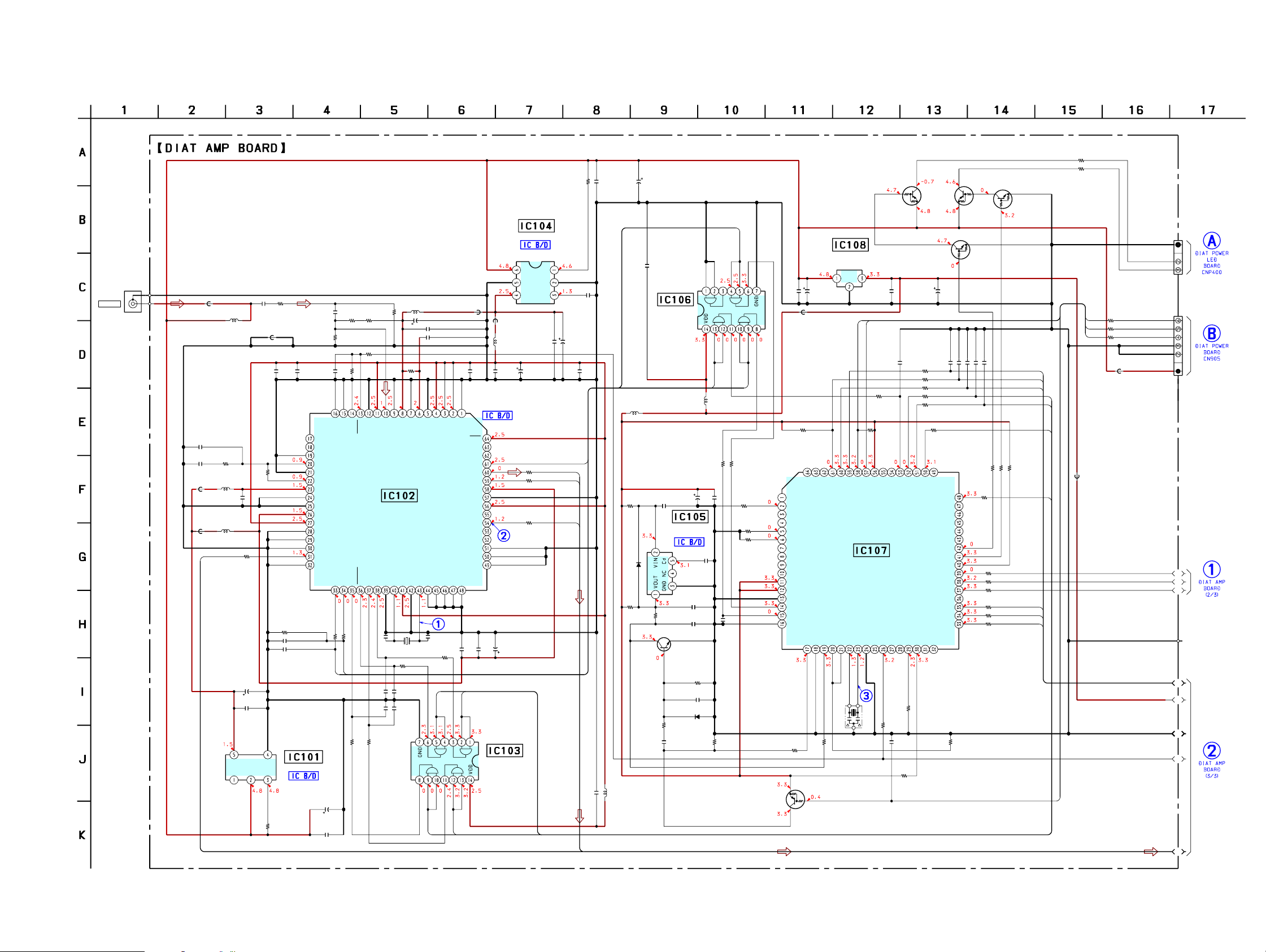
3-2. SCHEMATIC DIAGRAM – DIAT AMP Board (1/3) –
(1/3)
J100
DIR-R1
FB101
FB102
FB109
C111
0.01
C110
R102
0.1
820
L102
10µH
L103
10µH
APX
C105 R311
L101
0.01
47µH0
FB110
C113
0.1
R104
3.3k
C108
0.1
R103
330
R105
C115
C114
C104
47
16V
C103
0.1
VOUT VSS
NC VIN CE
+1.5V REGULATOR
R101
10k
XC62HR1502MR
47k
0.001
0.001
IC101
R312
4.7k
C116 R109
0.1 3.3k
PLREF
PLVAR
TESTMD
APVCI
VSS
APCPO
APAVD
APAVS
VSS
VDDI
VDDE
VCOR
CHNUM
DIVCODE
APX
EXTCK
C102
10
50V
C101
0.1
R313 R314C120
2.2k 4.7k0.01
XRST
DIFM1
DIFM0
DTSEL
SWDT
SRDT
CSOD
XSCEN
100
100
R106
R108
SRDT
CSOD
• See page 8 for Waveforms. • See page 16 for IC Block Diagrams. • See page 18 for IC Pin Function Description.
C137
10
50V
C149
0.1
L108
10µH
R128
10k
D110
1SS355
R122 C148
10k 0.1
R121
2.2k
L106
10µH
LEVEL SHIFT
TC74VHCT08
C146
0.1
IC106
AFT(EL)
2SC1623-T1
RESET SWITCH
R123
22k
C150
100
10V
VOLTAGE
DETECTOR
IC105
PST3629NR
Q102
-L5L6
MA111-TX
L107
10µH
C152
0.1
R124
C147
0.001
D102
SRDT
C151 R127
0.1 47k
C145
0.22
C156
100p
47k
Q111
DTA114EKA-
T146
DTVALID
C162
0.01
FB105
CSOD
R126R139
1k100
NC
MOD2
R257
47k
R258
47k
NC
NC
MODEL
SIMUKE
NC
NC
NC
NC
AVCC
AVR
AVSS
DTVALID
CSOD
NC
R152R171C143
10047k0.1
+3.3V REGULATOR
IC108
µPC2933T-E2
OI
G
OFF
CONT
V_CONT
DAMP_LATCH
SURROUND AMP
CONTROLLER
MB89537APFM
-G-565-BNDE1
X1
X0
C160
0.01
R143
0
R135
10k
SE
VCC
T_SEN
MAIN_OFF
IC107
XRST_INIT
FS2_EX
VSS
R142
100
100
10V
R256
3.3k
NC
SI2
INT24
DAMP_SCDT
DAMP_SHIFT
AC CUT
/RESET
MOD1
MOD0
NC
X102
8MHz
R129 C253 R131
100 0.22 47k
Q110
DTA114EKA-
T146
AC CUT
R111
220
R110
1k
VSS
VDDE
ADVIN
RF DEMODULATOR
A/D CONVERTER
VSS
SCMODE
SCLK
C124 C129
10p 33p
C122 C125
100p 100p
R113R112
100100
R116
68
ADVRL
IC102
CXD4017R
OSCI
12.288MHz
R117 C138
10k 0.1
+2.5V REGULATOR
IC104
TK11225CMCL-G
CNT
GND
GND
L104 10µH
C128
47 16V
C132
C131
VSS
VDDE
ADAVS
ADAVD
ADVRH
TEST1
TEST0
OSCO
VSS
VDDE
X101
R114
100
C126C123
100p100p
XSCEN
D_SWDT
FB103
DAOUT
TXOUT
TEST7
TEST6
TEST5
0.1100
FB104
L105
10µH
C134
C130C119
1
0.10.1
XTST
LRCK
VDDI
VSS
VDDE
BCK
ICLK
C107
C109
47
0.1
16V
LEVEL SHIFT
IC103
TC74VHCT08
AFT(EL)
1
1
MST
XSM
SMCK
EMPFS1
EMPFS0
DTVALID
SYMCLK
TEST4
TEST3
TEST2
C141R115
SCMODE
D_SCLK
CNPINOUT
C135
0.1
C140
10
50V
R120
1k
R118
1k
R119
1k
DTVALID
DAOUT
LRCK
BCK
C142
0.01
C136
47
16V
C127
0.1
C133
0.1
Q103,104,111,112
LED DRIVE
Q112 Q104
DTA114EKA-
T146
Q103
DTC114EKA-
T146
C161C163
100
16V
100p
100p
100p
C157
R140
100
R138
R137
R144
R145
R141
DT
DT
NC
NC
R253
47k
R252
10k
DIAT_SR
NC
DIAT_SCLK
DIAT_SW
DAMP_NSPMUTE
DAMP_SOFTMUTE
DAMP_PGMUTE
P22
P23
NC
XSCEN
SCMODE
LED_RED
LED_GREEN
DRIVE_OTW
DRIVE_OCP
DRIVE_RST
NC
NC
100p
10p
C153
C155
C158
C154
100
100
100
100
100
R151
NC
NC
NC
NC
NC
P10
DTC114EKA-
T146
100p
C159
SCLATCH
SCDT
SCSHIFT
D_SWDT
D_SCLK
XSCEN
100
100
10k
R150
R149
R254
100
SCMODE
R260
100
R261
100
R262
100
R148
100
N-MUT
R147
100
S-MUT
R146
100
P-MUT
CUT
R100
150
R125
150
CNP102
3P
GND
RED
GRN
(Page 15)
CNP103
6P
MAIN-OFF
1k
AC-CUT
1k
V-CONT
100
DGND
DGND
5V
(Page 15)
A1
A2
A3
FB106
R165
OFF
CUT
R259
CONT
R136
FB107
(Page 10)
EB102
B1
B2
B3
B4
(Page 11)
TA-SB500WR
B5
99
TA-SB500WR
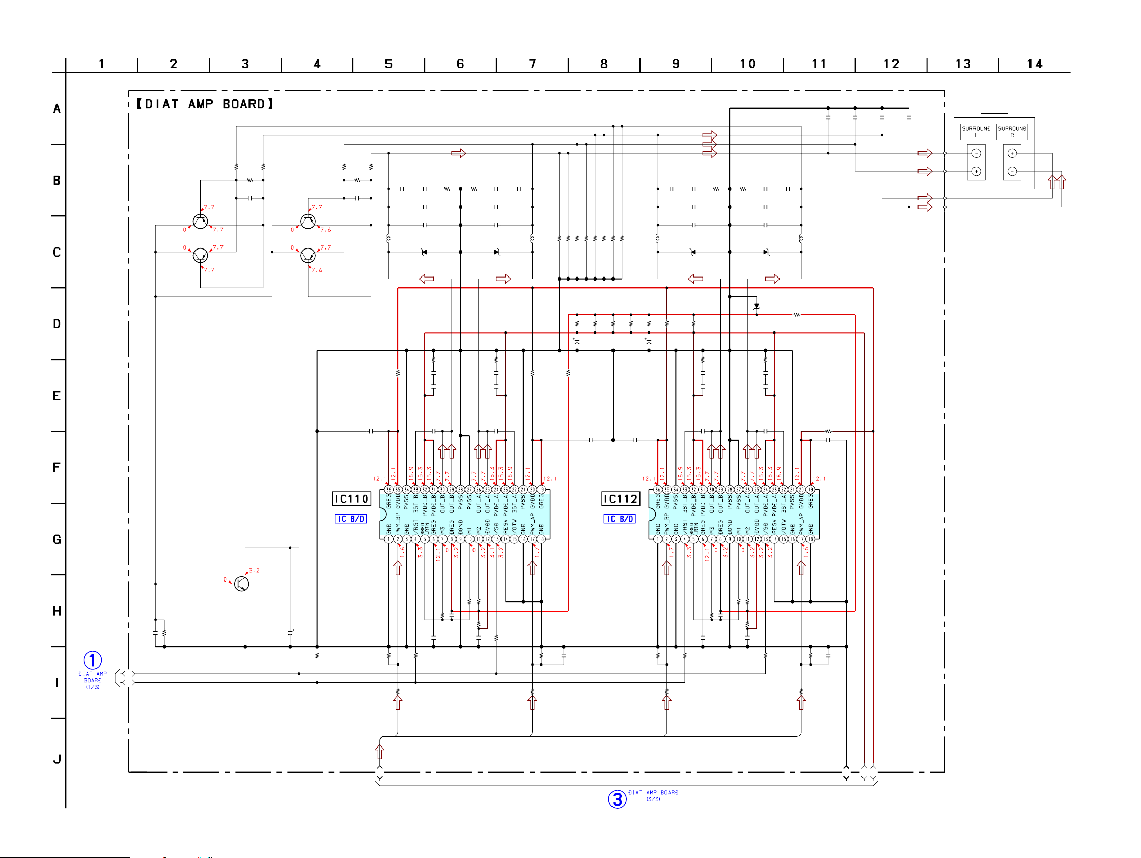
3-3. SCHEMATIC DIAGRAM – DIAT AMP Board (2/3) –
(2/3)
R153 R156
100k 100k
R154
100k
C165
Q106
2SA1602TP-
1EF
Q105
2SA1602TP-
1EF
2.2
Q105,106,108,109
OVER LOAD DETECT
Q109
2SA1602TP-
1EF
Q108
2SA1602TP-
1EF
• See page 16 for IC Block Diagrams.
R159R157
R158
100k
100k
100k
C169
2.2
L112
10µH
C183 R169C182
0.0022 2.70.0022
C185 C193
0.047 0.047
C184
1
C181R164
0.220
C180
0.22
C189R177 C194
0.00222.7 0.0022
C192
1
D105D104
P6SMBJ33A-5P6SMBJ33A-5
R180R167
3.33.3
C191
0.22
C190
0.22
10k
10k
R204
R205
L115
10µH
R185 R220
0 100
10k
R206
T100
C259C258C257C256
0.010.010.010.01
R195 C218 C224R191C210C209
2.7 0.0022 0.00222.70.00220.0022
C213
0.047
C212 C216
10k
10k
10k
10k
10k
R208
R207
R209
R210
R211
L118
10µH
C235C199
2200
35V
2200
35V
11
R225R224R219R218R217R216
R186
10k10k10k10k10k10k
0
C208
0.22
C207
0.22
C217
0.047
R222
L121
10µH
100
D107D106
P6SMBJ33A-5P6SMBJ33A-5
D115
MA8027
R198R189
3.33.3
C222
0.22
C221
0.22
SPEAKER
(Page 9)
R203
C238
0
1
R196
C231C203
0.0330.033
0
0
R192
R193
100
C215
0.01
C170
1
POWER DRIVER
IC110
CXD9774M
Q107
2SC1623-T1
-L5L6
PROTECT
DETECT
R155C166
100k2.2
A2
A3
C168
47
16V
R263
4.7k
R212 R166
22k 0
C177 C197
0.033 0.033
0
R168
C243 C188
0.1 0.01
R173
560
C201C200
11
POWER DRIVER
IC112
CXD9774M
0
0
R174
R176
R178
100
0.1
C186
R179
0
R213 C240
22k 47p
R175 R181 R183
560 560 560
R214 R215 C242R197
22k 22k 47p0
C244
R188
0
0.1
R190
0.1
C211
0
TA-SB500WR
OUTL2
C1
OUTL1
OUTR2
OUTR1
C2
C4
C3
(Page 11)
1010
TA-SB500WR
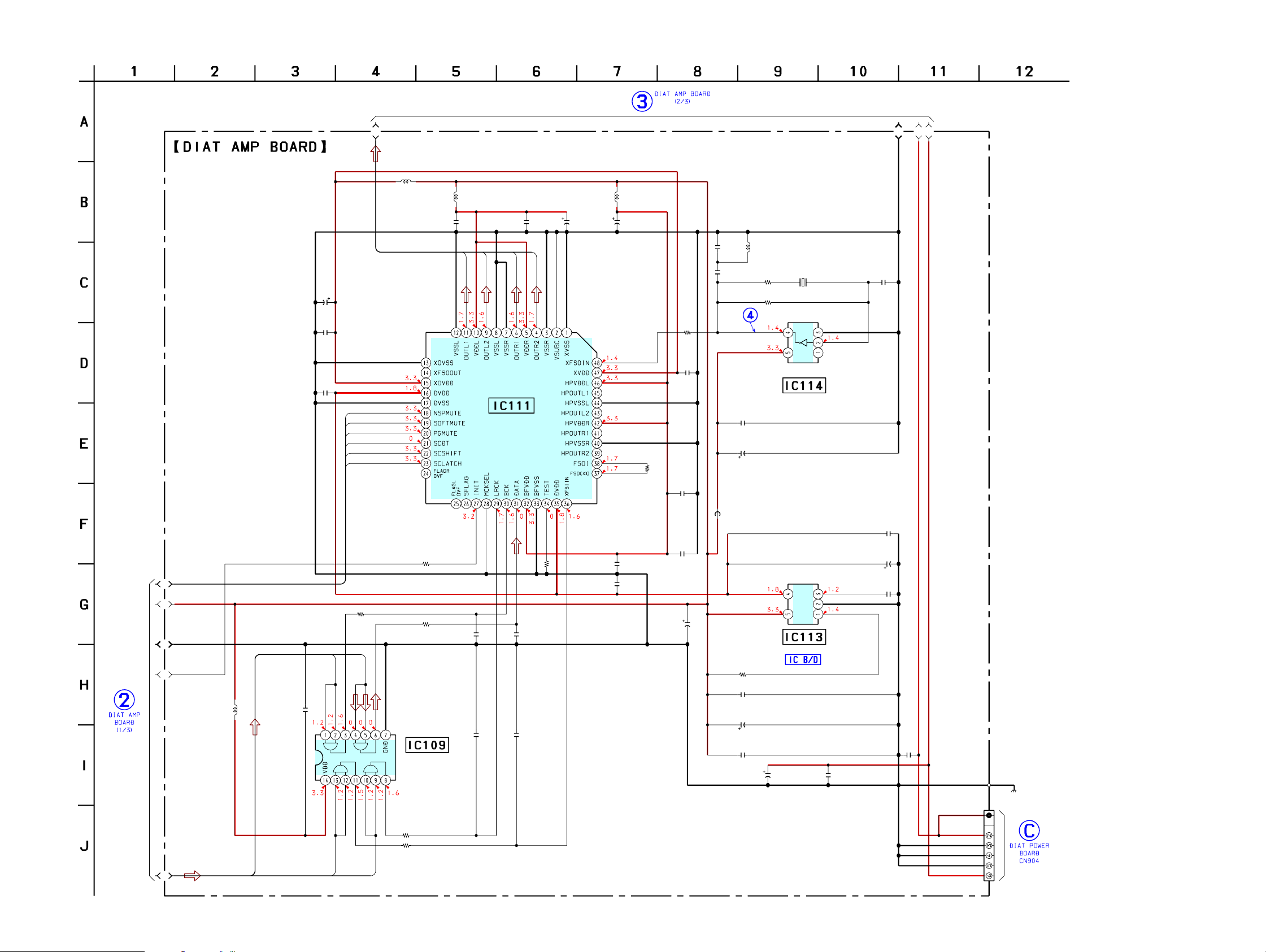
3-4. SCHEMATIC DIAGRAM – DIAT AMP Board (3/3) –
(3/3)
C178
47
16V
C173
0.1
C176
0.1
N-MUT
S-MUT
P-MUT
SCDT
SCSHIFT
SCLATCH
• See page 8 for Waveform. • See page 16 for IC Block Diagram.
(Page 10)
C1
L110
10µH
L111
10µH
OUTL1
C187C196
OUTL2
STREAM PROCESSOR
IC111
CXD9788AR
L116
10µH
C202
C179
47
0.10.1
OUTR2
OUTR1
47
16V
16V
R187
0
R194
C206
C2
C3
C4
C220
L122
10p
1µH
C219 C237
0.001 5p
22
0.1
C233
0.01
C230
R201
R200
22
25V
100
1M
X103
49.152MHz
GND
VDD
IC114
MC74VHC1GU04
OSC
(Page 9)
C205
0.1
C204
R172
100
B1
B2
R163
100
B3
B4
L109
10µH
B5
C167
0.1
BCK
DAOUT
APX
LRCK
R161
R160
100
100
R162
100
LEVEL SHIFT
IC109
TC74VHCT08
AFT(EL)
C175
100p
C171
100p
R184 C198
0 0.1
C172
100p
C174
100p
C195
0.1
0.1
C214
FB108
IC113
NJM2870F18
VOUT
N.B.
GND
VIN
+1.8V REGULATOR
C225
100
16V
CONT
C226
0.1
100
16V
R199
100k
C232
0.01
C228
100
10V
C227 C236
0.1 0.1
C223
0.01
C229
C234
0.01
100
16V
EB101
CNP106
(CHASSIS)
6P
30V
30V
GND
GND
GND
12V
(Page 15)
TA-SB500WR
1111
TA-SB500WR
• Semiconductor
Location
Ref. No. Location
D103 B-1
D104 C-6
D105 B-6
D106 B-6
D107 B-6
D115 B-5
IC108 B-4
Q103 B-3
Q104 B-3
Q106 C-8
Q109 C-8
Q110 A-1
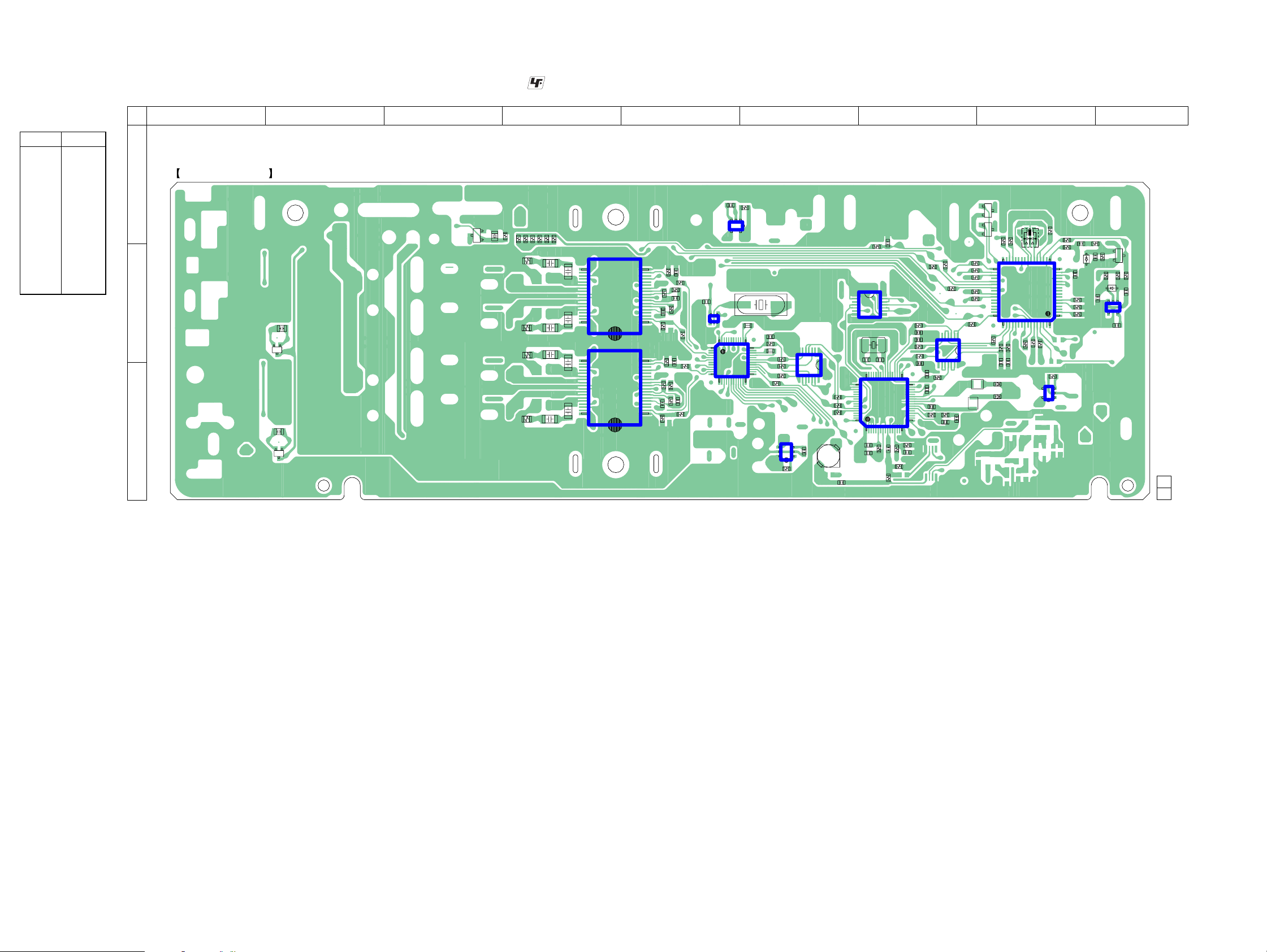
3-5. PRINTED WIRING BOARD – DIAT AMP Board (Component Side) –
1 2 3 4 5 6 7 8 9
DIAT AMP BOARD
(COMPONENT SIDE)
A
B
C
C165
E
Q105
E
Q108
C169
Q107
R155
C166
E
:Uses unleaded solder.
R217
R218
R225
R224
R219
R216
R198
C222
C221
19
C207
36
R189
C208
C191
R180
R167
C190
19
C180
36
C181
IC112
IC110
R193
R176
C243
18
1
18
1
R212
C244
R214
R215
R213
R174
R168
C242
R183
R192
C211
R190
IC114
R181
C240
R175
C186
R173
C233
1
12
C234
54
13
48
13
IC111
R199
13
IC113
54
R187
37
24
X103
36
R184
25
C174
R160
R162
R172
IC104
R117
R161
IC109
R163
C142
43
61
17
148
R119
R118
R120
L101
49
64
C131
C132
C105
1
7
R259
IC106
X101
C129
IC102
1
R116
14
8
C124
C120
R111
R311
C253
C123
C126
R114
R112
3348
R110
16
R109
C116
R115
C122
C125
32
C108
17
R261
R104
C113
R262
R102
C111
R260
R113
R147
17
148
R148
R151
L102
C110
Q111
E
E
Q112
R146
33
R150
R149
48
R145
IC103
L103
FB101
X102
R253
R252
32 17
IC107
49 64
R141
R144
C159
C158
FB102
R140
R135
4
5
IC101
R137
R101
R129
R131
R152
16
R257
1
3
1
D102
R258
R127
C143
C156
R123
C147
D110
C146
R124
Q102
E
R122
R128
R121
1
3
54
C145
1-862-468-
C148
IC105
12
(12)
TA-SB500WR
1212
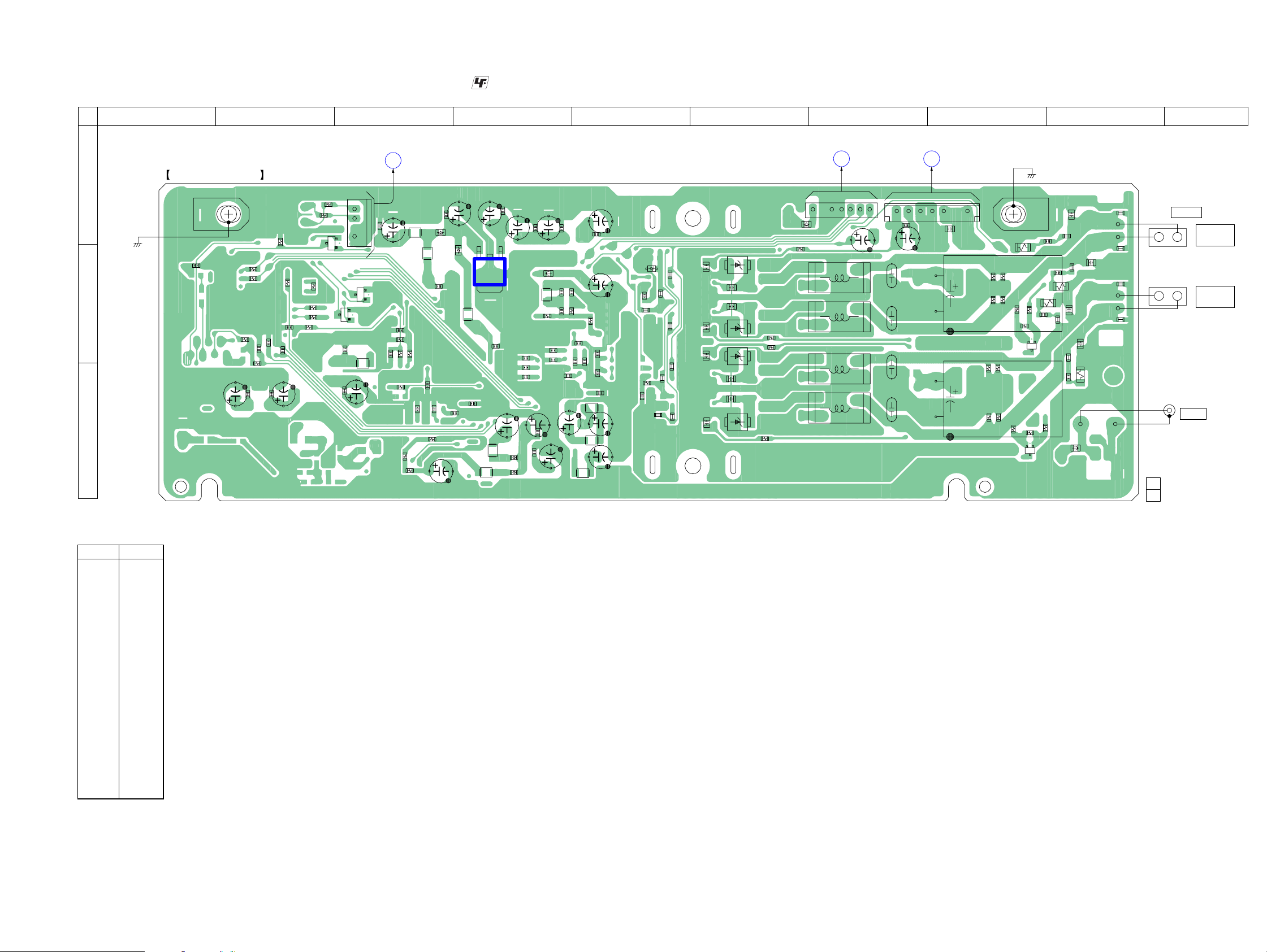
TA-SB500WR
3-6. PRINTED WIRING BOARD – DIAT AMP Board (Conductor Side) –
1 2 3 4 5 6 7 8 9 10
POWER LED
BOARD
A
C151
C150
C115
R105
C114
(Page 14)
R103
R313
CNP400
L108
R106
R314
L107
R108
C127
R312
C149
C130C119
C128
C160
FB105
FB106
IC108
C141
DIAT AMP BOARD
A
EB102
(CHASSIS)
B
C152
C102
C
(CONDUCTOR SIDE)
R139
R126
R256
C154
C155
R138
C103
C101
R171
C104
R142
C157
C153
CNP102
R125
R100
Q110
R254
R136
R165
R143
E
Q104
Q103
E
C133
C109
L106
C107
3
1
E
C161
:Uses unleaded solder.
C163
C162
C214
C227
13
2
L109
C167
C172
C175
C140
C171
FB104
FB103
C136
C135
C138
C134
L104
L105
C228
FB108
L122
R201
C137
C198
C195
C232
C220
C219
C176
C178
C206
C204
C205
L116
C237
R194
R200
C223
C196
C229
C230
C187
C173
L111
L110
DIAT POWER
BOARD
B
CN905
(Page 14) (Page 14)
61
C168
CNP103
C231
C197
C177
C203
D107
D106
D105
D104
R164
R220
R197
R188
C238
C201
C200
C170
D115
C215
R196
C188
C179
C202
R222
R179
R178
R263
R166
FB107
R203
L121
L118
L115
L112
R186
R185
C226
C225
C216
C212
C192
C184
C
CNP106
DIAT POWER
BOARD
CN904
16
C236
C235
C199
R206
R204
R210
R208
R205
R209
R207
R159
R195
R211
R156
R154
EB101
E
R158
E
Q109
R153
C189
Q106
(CHASSIS)
C224
C218
C210
R191
R177
C194
R157
FB109
C182
C183
C217
C209
C193
C213
C185
R169
C259
C258
C257
C256
1-862-468-
(12)
T100
SPEAKER
SURROUND
–+
–+
12
J100
DIR-R1
R
SURROUND
L
• Semiconductor
Location
Ref. No. Location
D102 B-8
D110 B-9
IC101 C-8
IC102 C-7
IC103 B-7
IC104 C-6
IC105 B-9
IC106 B-7
IC107 B-8
IC109 C-6
IC110 C-4
IC111 B-5
IC112 B-4
IC113 A-5
IC114 B-5
Q102 B-9
Q105 B-2
Q107 A-3
Q108 C-2
Q111 A-8
Q112 A-8
TA-SB500WR
1313
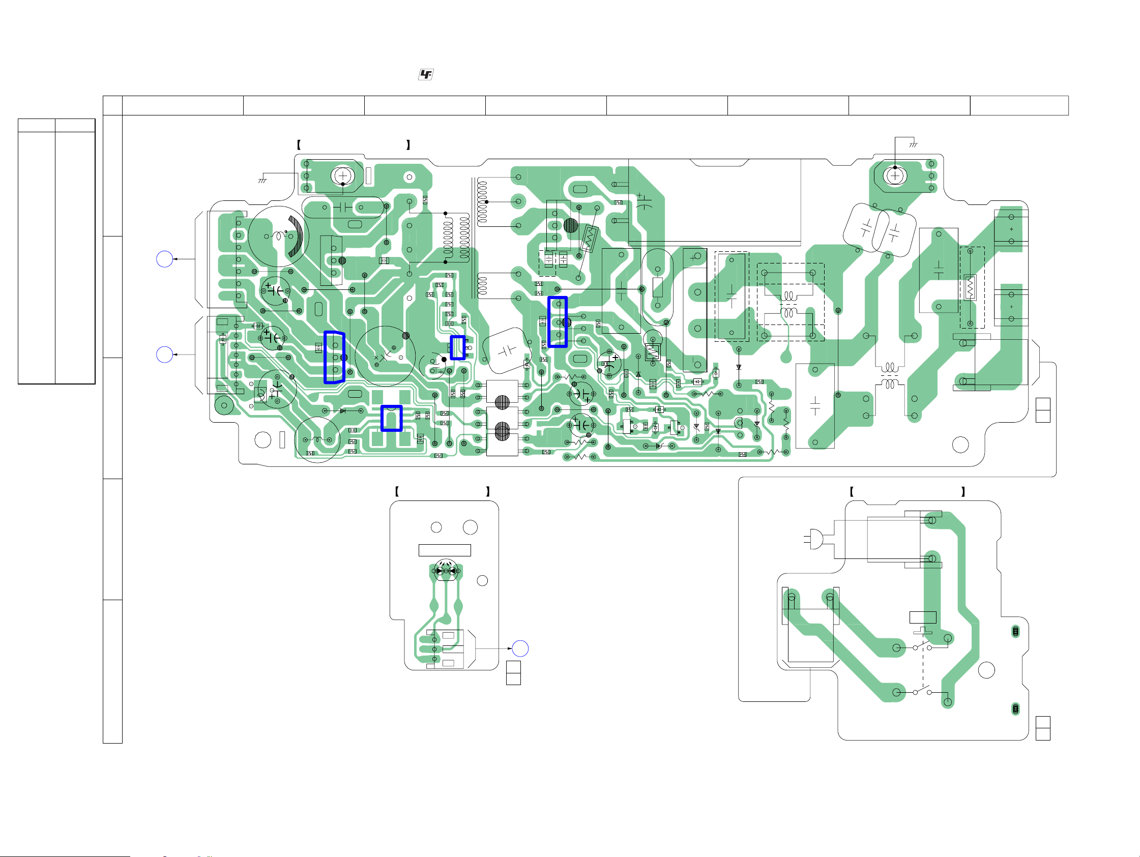
TA-SB500WR
• Semiconductor
Location
Ref. No. Location
D400 D-3
D901 B-5
D902 A-4
D904 C-5
D905 C-6
D906 C-5
D907 C-5
D908 C-5
D909 C-5
D910 C-4
D911 C-6
D913 C-5
D914 C-5
D915 C-5
D921 B-2
D922 C-2
D933 B-1
D934 B-2
IC901 B-4
IC903 B-2
IC904 C-3
IC905 B-3
Q901 C-6
Q902 C-5
Q903 C-5
3-7. PRINTED WIRING BOARDS – POWER SUPPLY Section –
1 2 3 4 5 6 7 8
DIAT POWER BOARD
A
B
C
C
DIAT AMP
BOARD
CNP106
(Page 13)
B
DIAT AMP
BOARD
CNP103
(Page 13)
CN904
D933
CN905
1
7
(CHASSIS)
D934
7
1
LP1
L901
C936
JW917
JW916
C941
L904
JW918
C938
C931
IC903
C937
HS2
L903
EB902
D921
A
K
A
JW915
1
2
3
D922
C940
JW912
C933
JW913
JW914
C932
IC904
1
4
R944
R942R943
:Uses unleaded solder.
T901
POWER
TRANSFORMER
R947
R934
R948
R935
R936
R932
IC905
R941
8
5
C942
R933
C934
C935
R940
JW911
R946
1
R945
R937
R931
JW910
R939
3
2
R938
JW909
(EXCEPT US, TW)
C925
D910
PC901
PC903
PC902
HS1
D902
A
K
C907
C918
R915
IC901
1
R916
C912
67
R911
R909
R912
JW908
JW905
R919
JW906
3
54
R922
R917
JW907
TH902
C910
R906
C909
R921
C913
C915
R907
C908
JW904
Q902
R920
C906
D904
JW903
C916
C917
E
TH901
R908
D913
D915
C911
Q903
D914
R910
JW902
C914
E
D901
D909
D906
R913
D907
R914
C905
E
D908
R926
(EXCEPT US, TW)
R904
R903
(TW)
R923
D911
R925
D905
Q901
R905
R924
LF902
(TW)
(EXCEPT TW)
JW901
C904
C903
LF901
EB901
(CHASSIS)
C902
(EXCEPT US)
C901
1
2
FH902
F901
R902
FH901
CN903
1-862-455-
11
(11)
D
E
DIAT LED BOARD
D400
POWER/ON LINE
CNP400
1
3
1-862-845-
A
11
(11)
DIAT AMP BOARD
CNP102
(Page 13)
(AC IN)
21
CN902
DIAT SWITCH BOARD
CN901
2
1
S901
POWER
1-862-456-
11
(11)
TA-SB500WR
1414
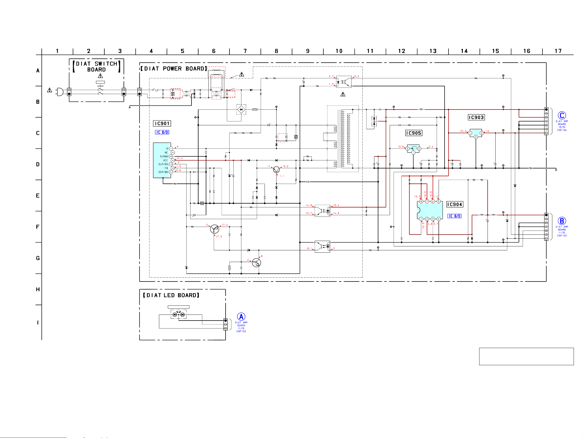
TA-SB500WR
3-8. SCHEMATIC DIAGRAM – POWER SUPPLY Section –
S901
POWER
CN902
CN903
F901
∗
F901
POWER CONTROL
IC901
R908
∗
0.15 2W (US, TW)
0.33 2W (EXCEPT US, TW)
(EXCEPT US)
R902
0.22
1/2W
275V
C902, 903
∗
470p 250V (EXCEPT US, TW)
2200p 250V (US, TW)
R907
0
2P
NUTRAL
(CHASSIS)
2P
EB901
∗
T3.15AL 250V (EXCEPT US, TW)
5A 125V (US, TW)
STR-W6735N (US, TW)
STR-W6765N (EXCEPT US, TW)
(AC IN)
CN901
2P
LIVE LIVE
NUTRAL
• See page 16 for IC Block Diagrams.
(TW)
R904
R903
C902
∗
LF901
1M
TP913
GND
R920
4.7k
UDZS-TE-17
C903
∗
C910
470p
R910
100
C909
2.2
50V
D913
-6.2B
C904C901
0.22
275V
(EXCEPT TW)
C908
3300p 1.2kV (US, TW)
680p 1.5kV (EXCEPT US, TW)
1k
R909
R908
∗
Q902
DTA114EKA
LF902
R911
1k
C912
0.1
R926
10k
Q902,903
OVER LOAD
PROTECT
TH902
(EXCEPT US, TW)
C905
275V
D3SB60F3
D915
MTZJ-T-77-33B
0.1
D901
∗∗∗
R905, R924, R925
∗
15k (US, TW)
22k (EXCEPT US, TW)
C907
∗
0.01 630V (US, TW)
3300p 630V (EXCEPT US, TW)
11EQS10
C913
22
50V
C914
0.0033
R921C917
68k0.01
UDZS-TE-17
C916
0.01
10EDB60
D908
1SS355
D914
-10B
PC902
PC123
R917 R922
∗∗
R917, R922
D911
R925R924R905
D907
R912
∗
47k (EXCEPT US, TW)
33k (US, TW)
R923
C906
∗
0
100 450V (EXCEPT TW)
330 200V (TW)
TP912
2SD1616A
REGULATOR
D909
1SS355
DTC144EKA
VIN
C906
∗
C918
C907
∗
D902
SARS03
MTZJ-T-77
Q901
+20V
C911
100p
100V
UDZS-TE-17
Q903
(EXCEPT US. TW)
D905
-33B
D910
-9.1B
3300p
630V
MTZJ-T-77
D904
11EQS10
R906
D906
-20B
TH901
R913
820
1k
∗
R914
4.7k
C915
R919
47
1.5k
35V
R906
∗
100k 2W (US, TW)
82k 2W (EXCEPT US, TW)
R916
22
R915
22
C925
0.001
250V
PC901
PC123
ISOLATOR
PC903
PC123
ISOLATOR
ISOLATOR
T901
POWER
TRANSFORMER
TP910
C931
VOUT
4700p
1kV
R931
22k
C934
0.01
D921
FML-22S
TP911
C932
C933
1000
0.1
35V
R938
1k
TP907
V-CONT
R945
TP909
2.2k
MAIN-OFF
GND
R939
1k
R940 R941
R932
3.3k
R933
47k
SHUNT REGULATOR
IC905
NJM431U
11
10µH
L901
R934
4.7k
R935
3.9k
R948
V+
ES
C940C942
220p0.1
R936 R937
2.2k 390
SI
CT
390
C936
100
35V
GND
DC/DC
CONVERTER
GND
IC904
NJM2374AE
C935
100
16V
IN+
CS
C937
0.1
R944
1k
R946
100
+12V REGULATOR
IC903
TA7812S
G
R942 R943
1.5k 1.5k
11EQS04
-TA1B
OI
TP902
GND
L903
220µH
C941
470
10V
D922
C938
100
16V
L904
10µH
UDZS-TE-17
TP908
AC-CUT
TP901
30V
TP904
12V
TP903
GND
D934
UDZS-TE-17
-18B
TP905
5V
D933
-10B
TP906
DGND
CN904
7P
30V
30V
GND
GND
GND
12V
(Page 11)
R947
0
EB902
(CHASSIS)
CN905
7P
5V
DGND
DGND
V-CONT
AC-CUT
MAIN-OFF
(Page 9)
TA-SB500WR
D400
SPR-54MVWF
POWER/ON LINE
GREEN
CNP400
3P
GND
RED
(Page 9)
The components identified by mark 0 or dotted
line with mark 0 are critical for safety.
Replace only with part number specified.
1515
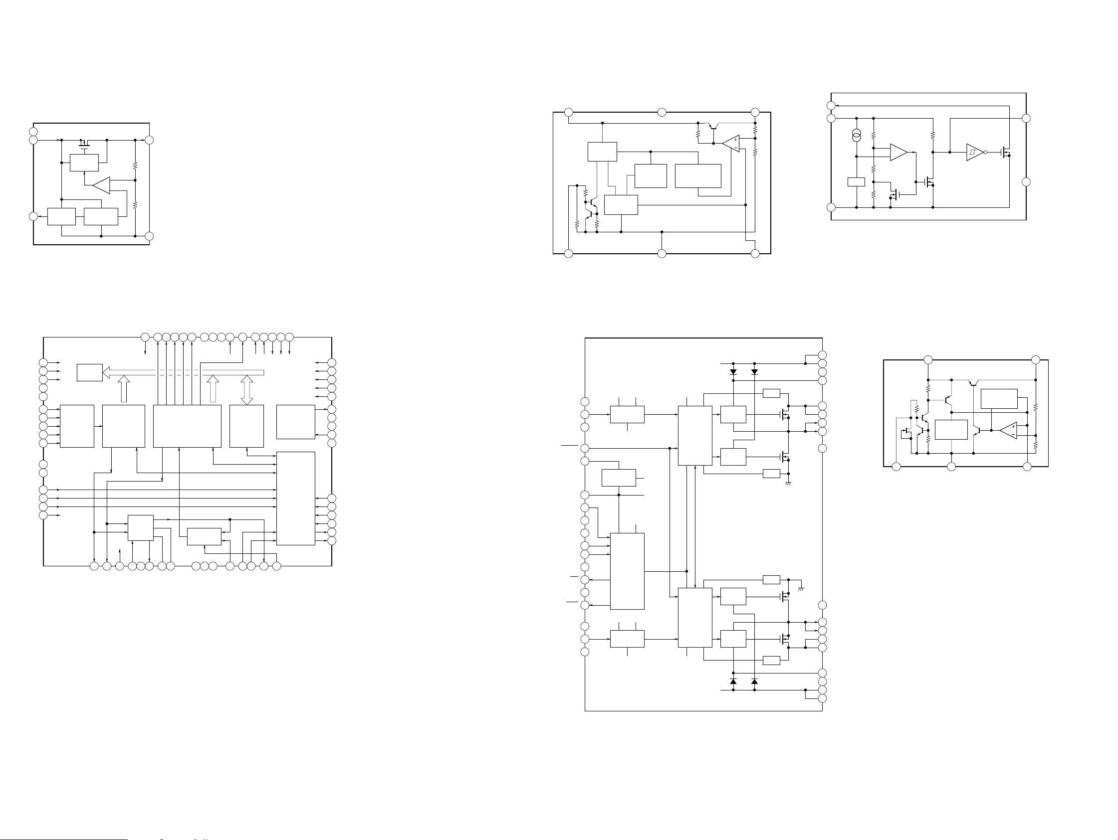
TA-SB500WR
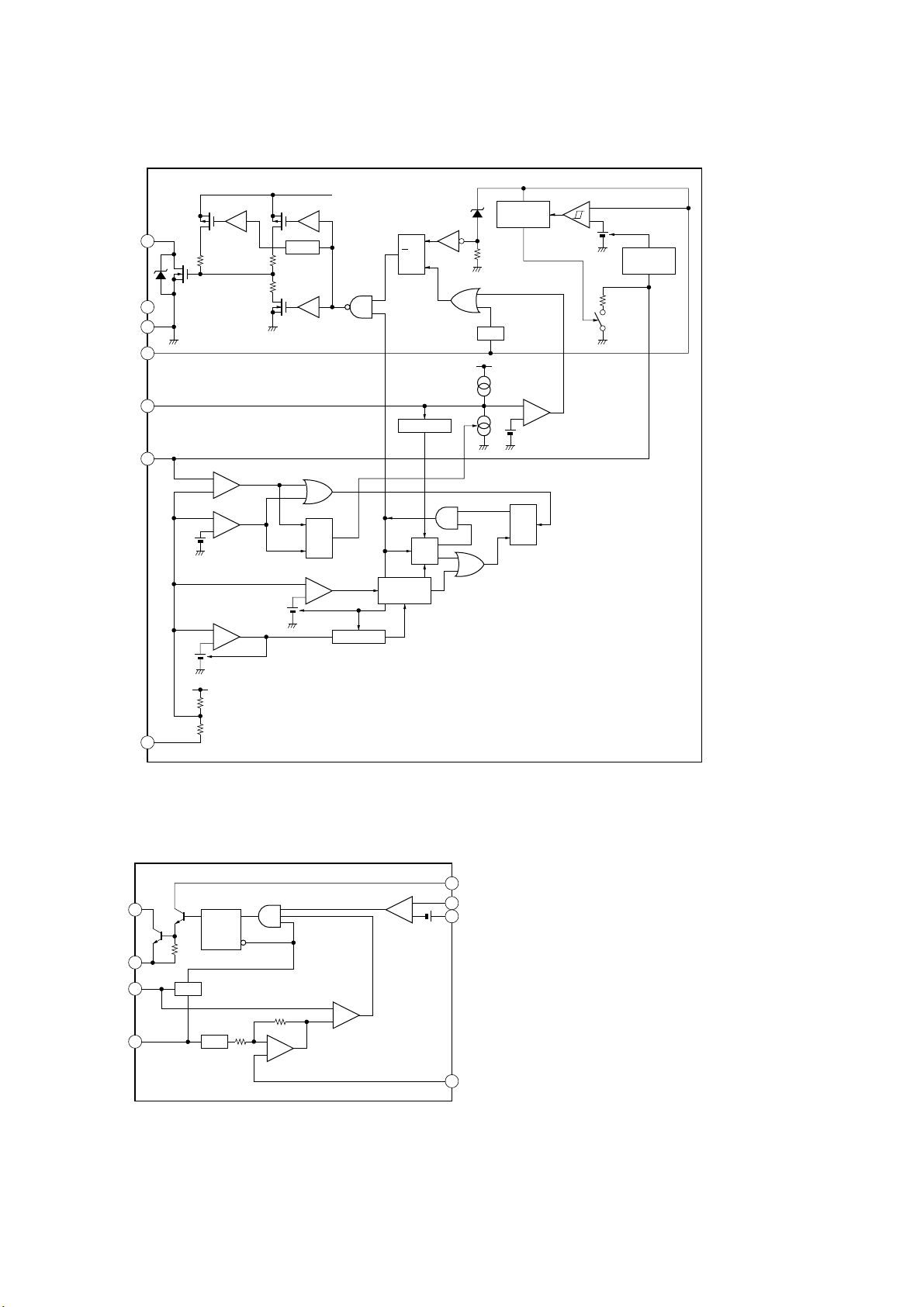
• IC Block Diagrams
– DIAT AMP Board –
IC101 XC62HR1502MR
NC
1
VIN
2 5
CURRENT
LIMIT
+
–
CE
OUTPUT
3
CONTROL
REFERENCE
VOLTAGE
IC102 CXD4017R
TEST12 1
TEST13 2
TEST14
VDDE
VSS 5
ADVRH 6
ADAVS 7
ADAVD 8
ADVRL 9
ADVIN 10
VDDEE 11
VSS
XRST
DIFM0 14
DIFM1 15
TEST15 16
3
4
12
13
BUFFER
RAM
A/D
CONVERTER
DEMODULATOR
17
18
PLREF
PLVAR
19
TEST16
VOUT
VSS
4
TEST1164EMPFS163EMPFS062DTVALID61DAOUT60LRCK59VDDI58VSS57VDDE56BCK
OUTPUT
INTERFACE
20
PLL
21
APVCI
VSS
APCPO22APAVD
23
24
APAVS
CLOCK
SELECTOR
25
26
VSS
VDDI
27
TEST1055TEST953TEST852TEST751TEST650TEST5
54
ERROR
CORRECTOR
VCOR
29
30
CHNUM
DIVCODE
31
28
VDDE
CONTROLLER
32
APX
EXTCK
49
CLOCK
GENERATOR
IC104 TK11225CMCL-G
VIN
6 4
CONTROL
CIRCUIT
BANDGAP
REFERENCE
1 2 3
CONT
CONSTANT
CURRENT
SOURCE
GND
5
GND
OVER HEAT &
OVER CURRENT
PROTECT
VOUT
NP
IC110, 112 CXD9774M
TEST448
TEST347
TEST246
TEST145
TEST044
OSCO43
42
VSS
VDDE
41
OSCI40
VSS
39
DREG RTN 5
SCMODE38
SCLK37
XSCEN36
SWDT35
SRDT34
CSOD33
GND
PWM BP
GND
RESET 4
GVDD
M3 7
DREG 8
DGND
M1 10
M2 11
DVDD
DGND
OTW 15
GND
PWM AP
GND
1
2
3
6
9
12
SD 13
14
16
17
18
DREG DREG
DVDD
PWM
RECEIVER
DGND
DIGITAL
REGULATOR
DREG
PROTECTION
LOGIC
OT
&
UVP
DVDD DREG
PWM
RECEIVER
DGND
DREG
GVDD
TIMING
CONTROL
&
PROTECTION
TIMING
CONTROL
&
PROTECTION
DREG
GVDD
GVDD
GATE
DRIVE
GATE
DRIVE
GATE
DRIVE
GATE
DRIVE
OCH
OCL
OCL
OCH
IC105 PST3629NR
OUT
1
VDD 2
VREF
3
GND
IC113 NJM2870F18 (TE2)
GVDD B36
GVDD B35
GND
34
BST B33
32
PVDD B
PVDD B
31
OUT B
30
OUT B
29
28
GND
GND
27
26
OUT A
25
OUT A
24
PVDD A
PVDD A
23
BST A
22
21
GND
GVDD A
20
GVDD A
19
–
+
1
CONTROL
VIN
5
REFERENCE
BANDGAP
2
GND
THERMAL
PROTECTION
4
3
NOISE
CD5
NC
VOUT
4
BYPASS
TA-SB500WR
1616
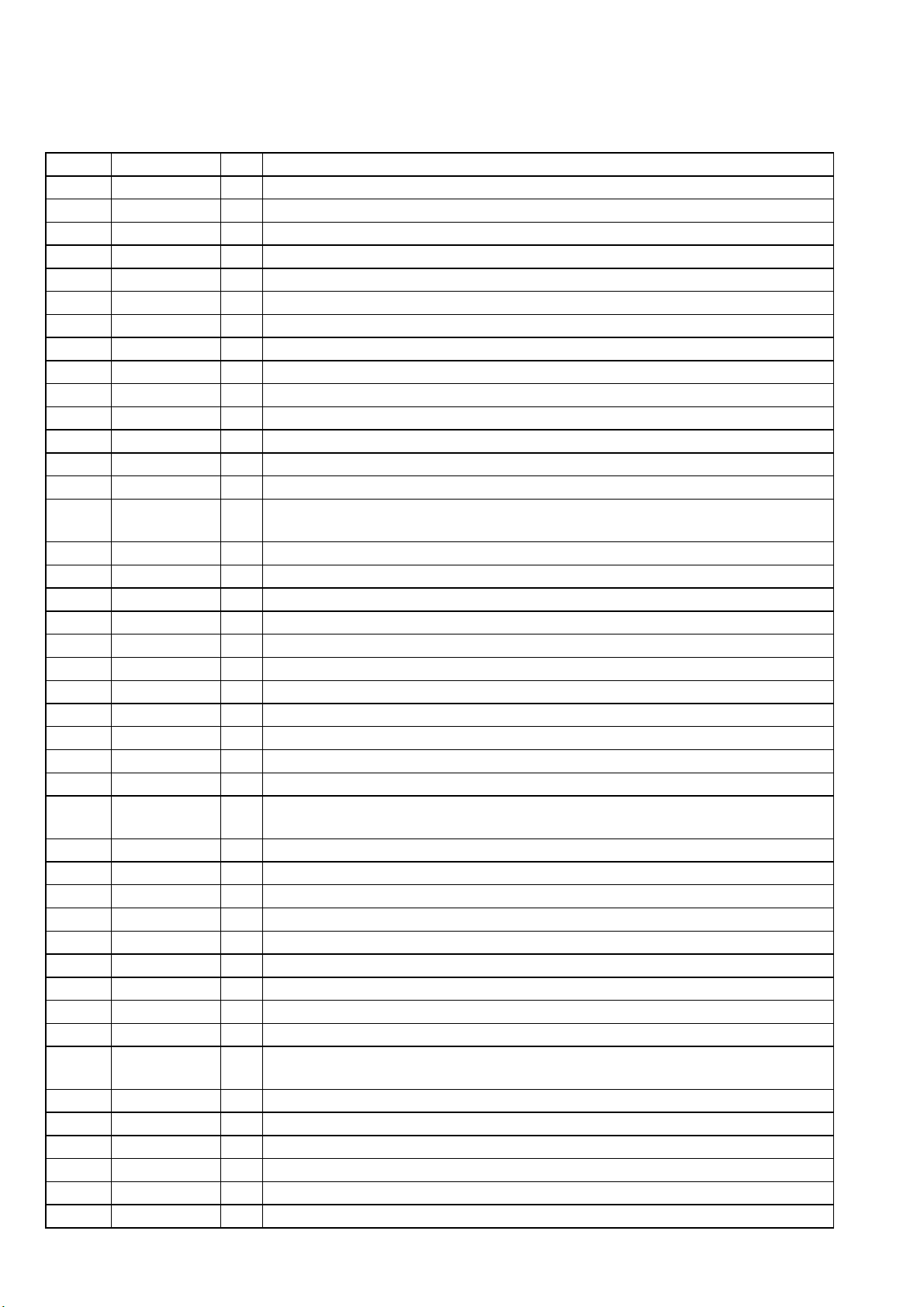
– DIAT POWER Board –
IC901 STR-W6765N
D 1
2
NC
3
S/GND
4
VCC
DELAY
DRIVE
REGULATOR
PROTECTION
LATCH
R
Q
S
REGULATOR
OVP
& ICONST
+
–
START/STOP
BURST
BURST
CONTROL
TA-SB500WR
SS/OLP
5
FB
OCP/BD
6
7
FB
+
–
OCP
–
+
BD
+
–
IC904 NJM2374AE (TE2)
OLP
+
SOFT START
S
Q
R
BSD
–
+
COUNTER
BOTTOM
SELECTOR
OSC
–
Q
R
S
CS 1
ES 2
CT
GND
CD8
+
QS
PWM
LOGIC
R
3
4
OSC
VREF
–
+
ERROR AMP
+
–
PWM
COMPARATOR
–
IPK SENSE
SI7
V+6
IN+5
17
TA-SB500WR
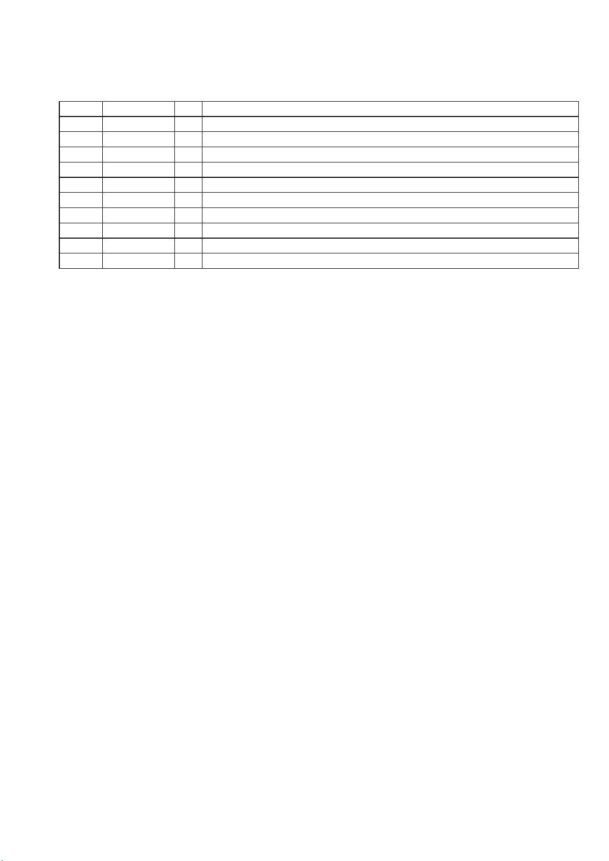
• IC Pin Function Description
DIAT AMP BOARD IC107 MB89537APFM-G-565-BNDE1 (SURROUND AMP CONTROLLER)
Pin No.
1
2
3, 4
5
6
7 to 10
11
12
13
14
15
16
17
18
19
20, 21
22
23
24
25
26
27, 28
29
30
31, 32
33
Pin Name I/O Description
NC
MOD2
NC
MODEL
SIMUKE
NC
AVCC
AVR
AVSS
DTVALID
CSOD
NC
AC CUT
NC
/RESET
MOD0, MOD1
X0
X1
VSS
FS2_EX
XRST_INIT
NC
P23
P22
NC
DAMP_PGMUTE
O
Not used
I
Setting terminal for the CPU operation mode Fixed at "L" in this set
O
Not used
I
Setting terminal for the model
I
Setting terminal for the destination
O
Not used
-
Power supply terminal (+3.3V) (for A/D converter)
I
Reference voltage (+3.3V) input terminal (for A/D converter)
-
Ground terminal (for A/D converter)
I
Data valid flag input from the RF demodulator "L": invalid, "H": valid
I
Captor start delay signal input from the RF demodulator "H" active
I
Not used
I
AC cut detection signal input terminal "L": AC cut
I
Not used
Reset signal input terminal "L": reset
I
For several hundreds msec. after the power supply rises, "L" is input, then it changes to "H"
I
CPU operation mode setting signal input terminal
I
Main system clock input terminal (8 MHz)
O
Main system clock output terminal (8 MHz)
-
Ground terminal
I
Not used
O
Reset signal output to the RF demodulator and stream processor "L": reset
O
Not used
I
Setting terminal for the CPU operation mode Fixed at "L" in this set
I
Setting terminal for the CPU operation mode Fixed at "H" in this set
O
Not used
O
PG muting on/off control signal output to the stream processor "L": muting on
34
35
36
37
38
39
40
41
42
43 to 47
48
49
50
51
52
53
54
DAMP_SOFTMUTE
DAMP_NSPMUTE
NC
DRIVE_RST
DRIVE_OCP
DRIVE_OTW
P10
LED_GREEN
LED_RED
NC
SCMODE
NC
XSCEN
DIAT_SCLK
DIAT_SWDT
DIAT_SRDT
NC
O
Soft muting on/off control signal output to the stream processor "L": muting on
O
NSP muting on/off control signal output to the stream processor "L": muting on
O
Not used
O
Reset signal output to the power driver "L": reset
I
Shut down state input from the power driver "L": shut down
I
Overtemperature warning signal input terminal Not used
I
Setting terminal for the CPU operation mode Fixed at "H" in this set
O
LED drive signal output of the ON LINE indicator "H": LED on
O
LED drive signal output of the POWER indicator "H": LED on
O
Not used
Control mode selection signal output to the RF demodulator
O
"L": pin setting, "H": serial setting
-
Not used
O
Serial interface enable signal output to the RF demodulator
O
Serial interface data clock signal output to the RF demodulator
O
Serial interface data write signal output to the RF demodulator
I
Serial interface data read signal input from the RF demodulator
O
Not used
18
TA-SB500WR
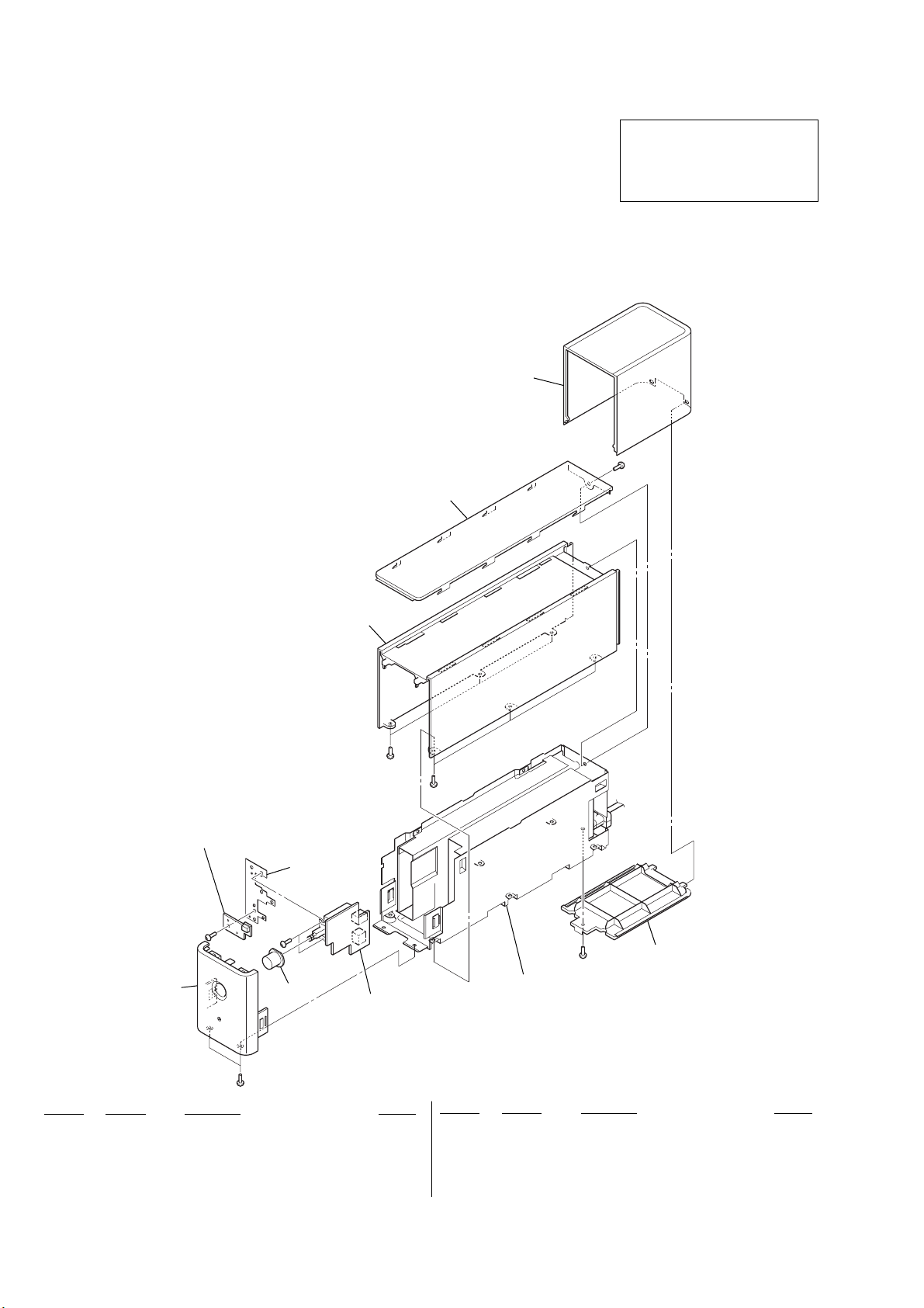
Pin No.
55
56
57
58
59
60
61
62
63
64
Pin Name
T_SENSE
VCC
MAIN_OFF
V_CONT
DAMP_LATCH
DAMP_SHIFT
DAMP_SCDT
SI2
INT24
NC
I/O
O
Not used
-
Power supply terminal (+3.3V)
O
Power off control signal output to the power control "H": power off
O
Voltage control PWM signal output to the shunt regulator
O
Latch control signal output to the stream processor
O
Shift clock signal output to the stream processor
O
Serial data output to the stream processor
I
Serial data input terminal
O
Not used
O
Not used
Description
19
TA-SB500WR
SECTION 4
EXPLODED VIEWS
NOTE:
• -XX and -X mean standardized parts, so they
may have some difference from the original
one.
• Color Indication of Appearance Parts
Example:
KNOB, BALANCE (WHITE) . . . (RED)
•Abbreviation
AUS: Australian model
HK : Hong Kong model
KR : Korean model
↑↑
Parts Color Cabinet's Color
RU : Russian model
SP : Singapore model
TW : T aiwan model
4-1. PANEL SECTION
• Items marked “*” are not stocked since they
are seldom required for routine service. Some
delay should be anticipated when ordering
these items.
• The mechanical parts with no reference
number in the exploded views are not supplied.
• Accessories are given in the last of the
electrical parts list.
not supplied
4
The components identified by mark
0 or dotted line with mark 0 are
critical for safety.
Replace only with part number
specified.
#2
not supplied
(DIAT LED board)
#2
1
not supplied
#2
2
3
#2
#2
not supplied
(DIAT SWITCH board)
not supplied
#3
DIAT AMP/DIAT POWER
boards section
#1
Ref. No. Part No. Description Remark
1 X-2022-678-1 FRONT SUB ASSY (EXCEPT US)
1 X-2050-558-1 FRONT SUB ASSY (US)
2 2-149-268-01 BUTTON, POWER
3 2-149-270-01 PANEL, SIDE (EXCEPT US)
3 2-149-270-11 SIDE, PANEL (US)
20
Ref. No. Part No. Description Remark
4 2-149-269-01 PANEL, TOP
#1 7-685-647-79 SCREW +BVTP 3X10 TYPE2 IT-3
#2 7-685-133-19 SCREW (DIA. 2.6) (IT3B)
#3 7-682-548-09 +B 3X8
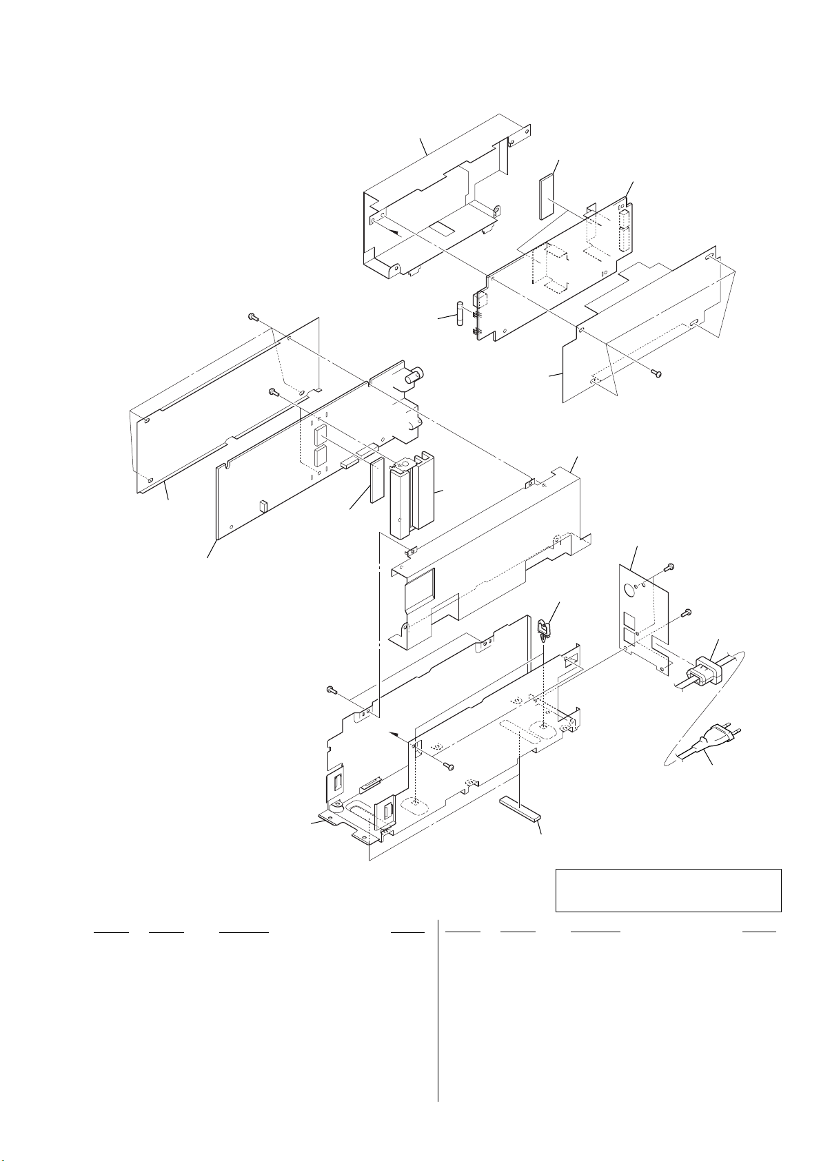
4-2. DIAT AMP/DIAT POWER BOARDS SECTION
not supplied
TA-SB500WR
56
52
not supplied
51
#2
#4
not supplied
#2
F901
not supplied
not supplied
not supplied
not supplied
#2
not supplied
#2
#1
53
not supplied
Ref. No. Part No. Description Remark
51 A-1068-892-A DIAT AMP BOARD, COMPLETE
52 A-1067-416-A DIAT POWER BOARD, COMPLETE (TW)
52 A-1068-894-A DIAT POWER BOARD, COMPLETE
(EXCEPT US, TW)
52 A-1079-747-A DIAT POWER BOARD, COMPLETE (US)
53 4-217-350-11 STOPPER, CORD
0 54 1-696-169-31 CORD, POWER (AEP, UK, RU, HK, SP)
0 54 1-696-847-22 CORD, POWER (AUS)
0 54 1-769-079-32 CORD, POWER (KR)
0 54 1-783-531-72 CORD, POWER (US)
0 54 1-827-597-41 CORD, POWER (TW)
#2
54
55
The components identified by mark 0 or dotted
line with mark 0 are critical for safety.
Replace only with part number specified.
Ref. No. Part No. Description Remark
55 2-149-284-01 FOOT
56 4-254-954-01 SHEET (DMB), RADIATION
0 F901 1-532-465-33 FUSE (T3.15AL/250V) (EXCEPT US, TW)
0 F901 1-533-420-12 FUSE, GLASS CYLINDRICAL (DIA. 5) (5A/125V)
0 F901 1-533-453-12 FUSE, GLASS TUBE (DIA. 5) (5A/125V) (TW)
#1 7-685-647-79 SCREW +BVTP 3X10 TYPE2 IT-3
#2 7-685-133-19 SCREW (DIA. 2.6) (IT3B)
#4 7-685-645-79 SCREW +BVTP 3X6 TYPE2 IT-3
(US)
21

TA-SB500WR
DIAT AMP
SECTION 5
ELECTRICAL PARTS LIST
NOTE:
• Due to standardization, replacements in the
parts list may be different from the parts
specified in the diagrams or the components
used on the set.
• -XX and -X mean standardized parts, so they
may have some difference from the original
one.
• RESISTORS
All resistors are in ohms.
METAL: Metal-film resistor .
METAL OXIDE: Metal oxide-film resistor.
F: nonflammable
•Abbreviation
TW : T aiw an model
Ref. No. Part No. Description Remark Ref. No. Part No. Description Remark
A-1068-892-A DIAT AMP BOARD, COMPLETE
*************************
< CAPACITOR >
C101 1-164-156-11 CERAMIC CHIP 0.1uF 25V
C102 1-126-964-11 ELECT 10uF 20% 50V
C103 1-164-156-11 CERAMIC CHIP 0.1uF 25V
C104 1-126-947-11 ELECT 47uF 20% 35V
C105 1-107-726-91 CERAMIC CHIP 0.01uF 10% 16V
C107 1-126-947-11 ELECT 47uF 20% 35V
C108 1-164-156-11 CERAMIC CHIP 0.1uF 25V
C109 1-164-156-11 CERAMIC CHIP 0.1uF 25V
C110 1-107-826-11 CERAMIC CHIP 0.1uF 10% 16V
C111 1-107-726-91 CERAMIC CHIP 0.01uF 10% 16V
C113 1-107-826-11 CERAMIC CHIP 0.1uF 10% 16V
C114 1-162-964-11 CERAMIC CHIP 0.001uF 10% 50V
C115 1-162-964-11 CERAMIC CHIP 0.001uF 10% 50V
C116 1-107-826-11 CERAMIC CHIP 0.1uF 10% 16V
C119 1-107-826-11 CERAMIC CHIP 0.1uF 10% 16V
C120 1-107-726-91 CERAMIC CHIP 0.01uF 10% 16V
C122 1-162-927-11 CERAMIC CHIP 100PF 5% 50V
C123 1-162-927-11 CERAMIC CHIP 100PF 5% 50V
C124 1-162-915-11 CERAMIC CHIP 10PF 0.5PF 50V
C125 1-162-927-11 CERAMIC CHIP 100PF 5% 50V
C126 1-162-927-11 CERAMIC CHIP 100PF 5% 50V
C127 1-107-826-11 CERAMIC CHIP 0.1uF 10% 16V
C128 1-126-947-11 ELECT 47uF 20% 35V
C129 1-162-921-11 CERAMIC CHIP 33PF 5% 50V
C130 1-107-826-11 CERAMIC CHIP 0.1uF 10% 16V
C131 1-125-837-11 CERAMIC CHIP 1uF 10% 6.3V
C132 1-125-837-11 CERAMIC CHIP 1uF 10% 6.3V
C133 1-107-826-11 CERAMIC CHIP 0.1uF 10% 16V
C134 1-125-837-11 CERAMIC CHIP 1uF 10% 6.3V
C135 1-164-156-11 CERAMIC CHIP 0.1uF 25V
C136 1-126-947-11 ELECT 47uF 20% 35V
C137 1-126-964-11 ELECT 10uF 20% 50V
C138 1-164-156-11 CERAMIC CHIP 0.1uF 25V
C140 1-126-964-11 ELECT 10uF 20% 50V
C141 1-107-826-11 CERAMIC CHIP 0.1uF 10% 16V
C142 1-107-726-91 CERAMIC CHIP 0.01uF 10% 16V
C143 1-107-826-11 CERAMIC CHIP 0.1uF 10% 16V
C145 1-115-467-11 CERAMIC CHIP 0.22uF 10% 10V
C146 1-107-826-11 CERAMIC CHIP 0.1uF 10% 16V
C147 1-162-964-11 CERAMIC CHIP 0.001uF 10% 50V
• Items marked “*” are not stocked since they
are seldom required for routine service.
Some delay should be anticipated when
ordering these items.
• SEMICONDUCTORS
In each case, u: µ, for example:
uA... : µA... uPA... : µPA...
uPB... : µPB... uPC... : µPC...
uPD... : µPD...
• CAPACITORS
uF: µF
• COILS
uH: µH
C148 1-107-826-11 CERAMIC CHIP 0.1uF 10% 16V
C149 1-107-826-11 CERAMIC CHIP 0.1uF 10% 16V
C150 1-104-665-11 ELECT 100uF 20% 25V
C151 1-107-826-11 CERAMIC CHIP 0.1uF 10% 16V
C152 1-107-826-11 CERAMIC CHIP 0.1uF 10% 16V
C153 1-162-927-11 CERAMIC CHIP 100PF 5% 50V
C154 1-162-915-11 CERAMIC CHIP 10PF 0.5PF 50V
C155 1-162-927-11 CERAMIC CHIP 100PF 5% 50V
C156 1-162-927-11 CERAMIC CHIP 100PF 5% 50V
C157 1-162-927-11 CERAMIC CHIP 100PF 5% 50V
C158 1-162-927-11 CERAMIC CHIP 100PF 5% 50V
C159 1-162-927-11 CERAMIC CHIP 100PF 5% 50V
C160 1-162-970-11 CERAMIC CHIP 0.01uF 10% 25V
C161 1-126-933-11 ELECT 100uF 20% 16V
C162 1-162-970-11 CERAMIC CHIP 0.01uF 10% 25V
C163 1-104-665-11 ELECT 100uF 20% 25V
C165 1-164-505-11 CERAMIC CHIP 2.2uF 16V
C166 1-164-505-11 CERAMIC CHIP 2.2uF 16V
C167 1-107-826-11 CERAMIC CHIP 0.1uF 10% 16V
C168 1-126-947-11 ELECT 47uF 20% 35V
C169 1-164-505-11 CERAMIC CHIP 2.2uF 16V
C170 1-164-346-11 CERAMIC CHIP 1uF 16V
C171 1-162-927-11 CERAMIC CHIP 100PF 5% 50V
C172 1-162-927-11 CERAMIC CHIP 100PF 5% 50V
C173 1-164-156-11 CERAMIC CHIP 0.1uF 25V
C174 1-162-927-11 CERAMIC CHIP 100PF 5% 50V
C175 1-162-927-11 CERAMIC CHIP 100PF 5% 50V
C176 1-164-156-11 CERAMIC CHIP 0.1uF 25V
C177 1-115-185-11 CERAMIC CHIP 0.033uF 10% 50V
C178 1-126-947-11 ELECT 47uF 20% 35V
C179 1-126-947-11 ELECT 47uF 20% 35V
C180 1-125-898-91 CERAMIC CHIP 0.22uF 10% 50V
C181 1-125-898-91 CERAMIC CHIP 0.22uF 10% 50V
C182 1-162-966-11 CERAMIC CHIP 0.0022uF 10% 50V
C183 1-162-966-11 CERAMIC CHIP 0.0022uF 10% 50V
C184 1-136-177-00 FILM 1uF 5% 50V
C185 1-163-035-00 CERAMIC CHIP 0.047uF 50V
C186 1-164-156-11 CERAMIC CHIP 0.1uF 25V
C187 1-164-156-11 CERAMIC CHIP 0.1uF 25V
C188 1-162-970-11 CERAMIC CHIP 0.01uF 10% 25V
C189 1-162-966-11 CERAMIC CHIP 0.0022uF 10% 50V
C190 1-125-898-91 CERAMIC CHIP 0.22uF 10% 50V
C191 1-125-898-91 CERAMIC CHIP 0.22uF 10% 50V
The components identified by mark
0 or dotted line with mark 0 are
critical for safety.
Replace only with part number
specified.
When indicating parts by reference
number, please include the board.
22
 Loading...