

Page 1
TA-FLX9W
SERVICE MANUAL
Ver 1.0 2004.07
TA-FLX9W is the amplifier section in DHC-FLX9W.
SPECIFICATIONS
Amplifier section:
Power ouput 40 watts/ch
1)
Depending on the sound field settings and the source,
there may be no sound output.
2)
Measured under AC 127, 240 V, 50/60 Hz
(Saudi Arabian model only)
Measured under AC 120, 240 V, 50/60 Hz
(except for Saudi Arabian model)
G
eneral
Power requirements
Saudi Arabian model: 120 – 127 V or 220 – 240 V
Thailand model: 220 – 240 V AC, 50/60 Hz
Other models: 110 – 120 V or 220 – 240 V
Power consumption
Dimensions (w/h/d)
Mass
(6 ohms at 1 kHz, 0.7%
THD)
60 watts/ch
(6 ohms at 1 kHz, 10%
THD)
AC, 50/60 Hz
Adjustable with voltage
selector
AC, 50/60 Hz
Adjustable with voltage
selector
92 watts
Approx. 95 × 156 ×
241 mm
Approx. 3.1 kg
E Model
2)
1)
2)
9-877-903-01
2004G05-1
© 2004.07
Design and specifications are subject to change
without notice.
REAR AMPLIFIER
Sony Corporation
Home Audio Company
Published by Sony Engineering Corporation
Page 2

TA-FLX9W
Notes on chip component replacement
• Never reuse a disconnected chip component.
• Notice that the minus side of a tantalum capacitor may be
damaged by heat.
UNLEADED SOLDER
Boards requiring use of unleaded solder are printed with the leadfree mark (LF) indicating the solder contains no lead.
(Caution: Some printed circuit boards may not come printed with
the lead free mark due to their particular size)
: LEAD FREE MARK
Unleaded solder has the following characteristics.
• Unleaded solder melts at a temperature about 40 °C higher
than ordinary solder.
Ordinary soldering irons can be used but the iron tip has to be
applied to the solder joint for a slightly longer time.
Soldering irons using a temperature regulator should be set to
about 350 °C.
Caution: The printed pattern (copper foil) may peel away if
the heated tip is applied for too long, so be careful!
• Strong viscosity
Unleaded solder is more viscou-s (sticky, less prone to flow)
than ordinary solder so use caution not to let solder bridges
occur such as on IC pins, etc.
• Usable with ordinary solder
It is best to use only unleaded solder but unleaded solder may
also be added to ordinary solder.
TABLE OF CONTENTS
1. GENERAL ................................................................... 3
2. DISASSEMBLY
2-1. Disassembly Flow ........................................................... 4
2-2. Case (Rear Amplifier) ..................................................... 4
2-3. VS Board ......................................................................... 5
2-4. RX Board......................................................................... 5
2-5. MAIN Board.................................................................... 6
3. DIAGRAMS
3-1. Block Diagram ................................................................ 7
3-2. Printed Wiring Board – RX Board – .............................. 9
3-3. Schematic Diagram – RX Board (1/2) – ........................ 10
3-4. Schematic Diagram – RX Board (2/2) – ........................ 11
3-5. Printed Wiring Boards – MAIN Section – ..................... 12
3-6. Printed Wiring Boards – POWER SUPPLY Section –... 13
3-7. Schematic Diagram – MAIN Section –.......................... 14
4. EXPLODED VIEWS
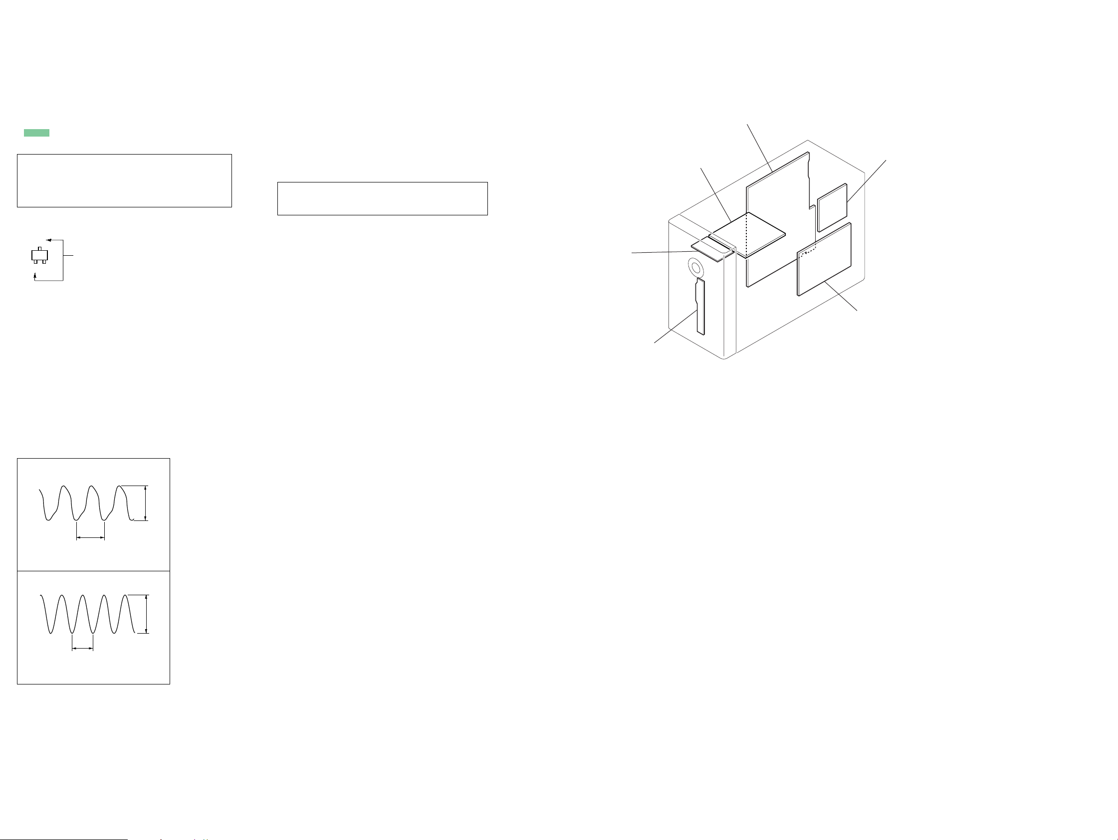
4-1. Front Panel Section ......................................................... 19
4-2. Chassis Section................................................................ 20
5. ELECTRICAL PARTS LIST................................ 21
SAFETY-RELATED COMPONENT WARNING!!
COMPONENTS IDENTIFIED BY MARK 0 OR DOTTED LINE
WITH MARK 0 ON THE SCHEMATIC DIAGRAMS AND IN
THE PARTS LIST ARE CRITICAL TO SAFE OPERATION.
REPLACE THESE COMPONENTS WITH SONY PAR TS WHOSE
PART NUMBERS APPEAR AS SHOWN IN THIS MANU AL OR
IN SUPPLEMENTS PUBLISHED BY SONY.
2
Page 3
SECTION 1
GENERAL
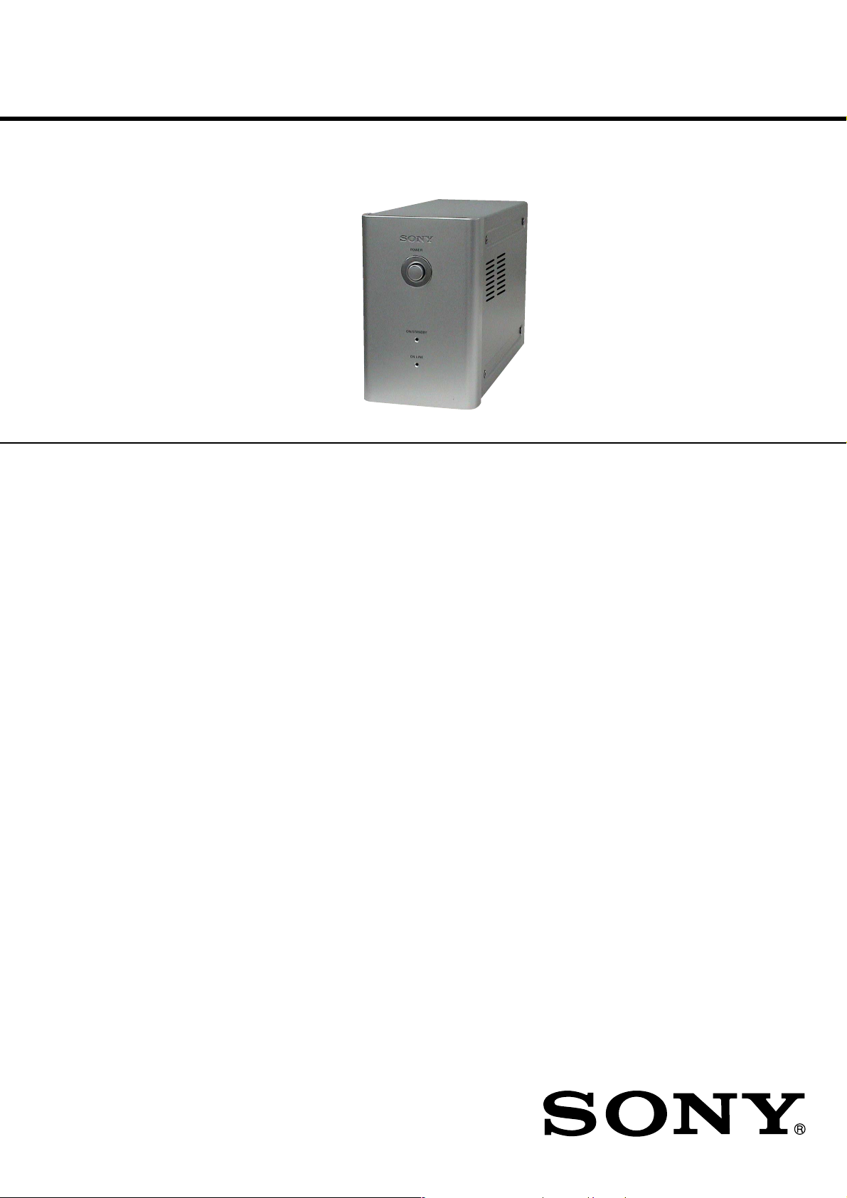
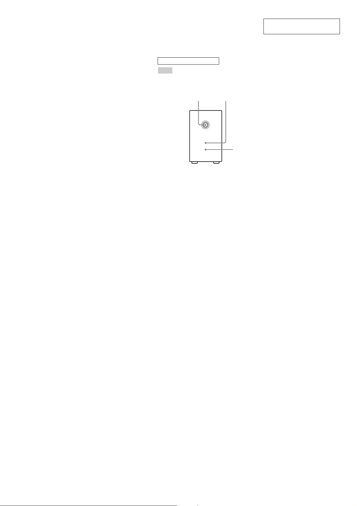
LOCATION OF CONTROLS
ALPHABETICAL ORDER
A – Z
ON LINE (indicator) 3
ON/STANDBY (indicator) 2
POWER 1
12
POWER
ON/STANDBY
ON LINE
TA-FLX9W
This section is extracted from
instruction manual.
3
3
Page 4
TA-FLX9W
• This set can be disassembled in the order shown below.
2-1. DISASSEMBLY FLOW
SET
2-2. CASE (REAR AMPLIFIER)
(Page 4)
2-3. VS BOARD
(Page 5)
2-4. RX BOARD
(Page 5)
2-5. MAIN BOARD
(Page 6)
SECTION 2
DISASSEMBLY
Note: Follow the disassembly procedure in the numerical order given.
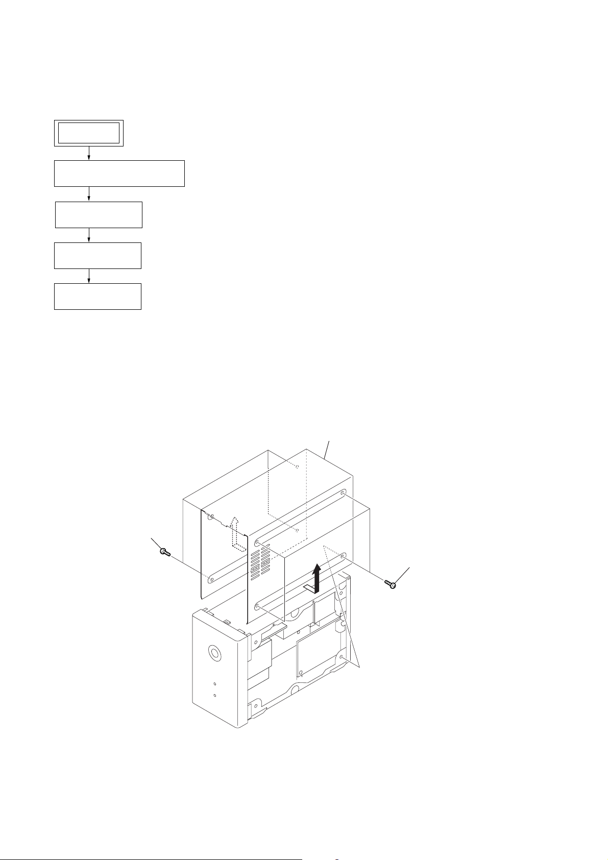
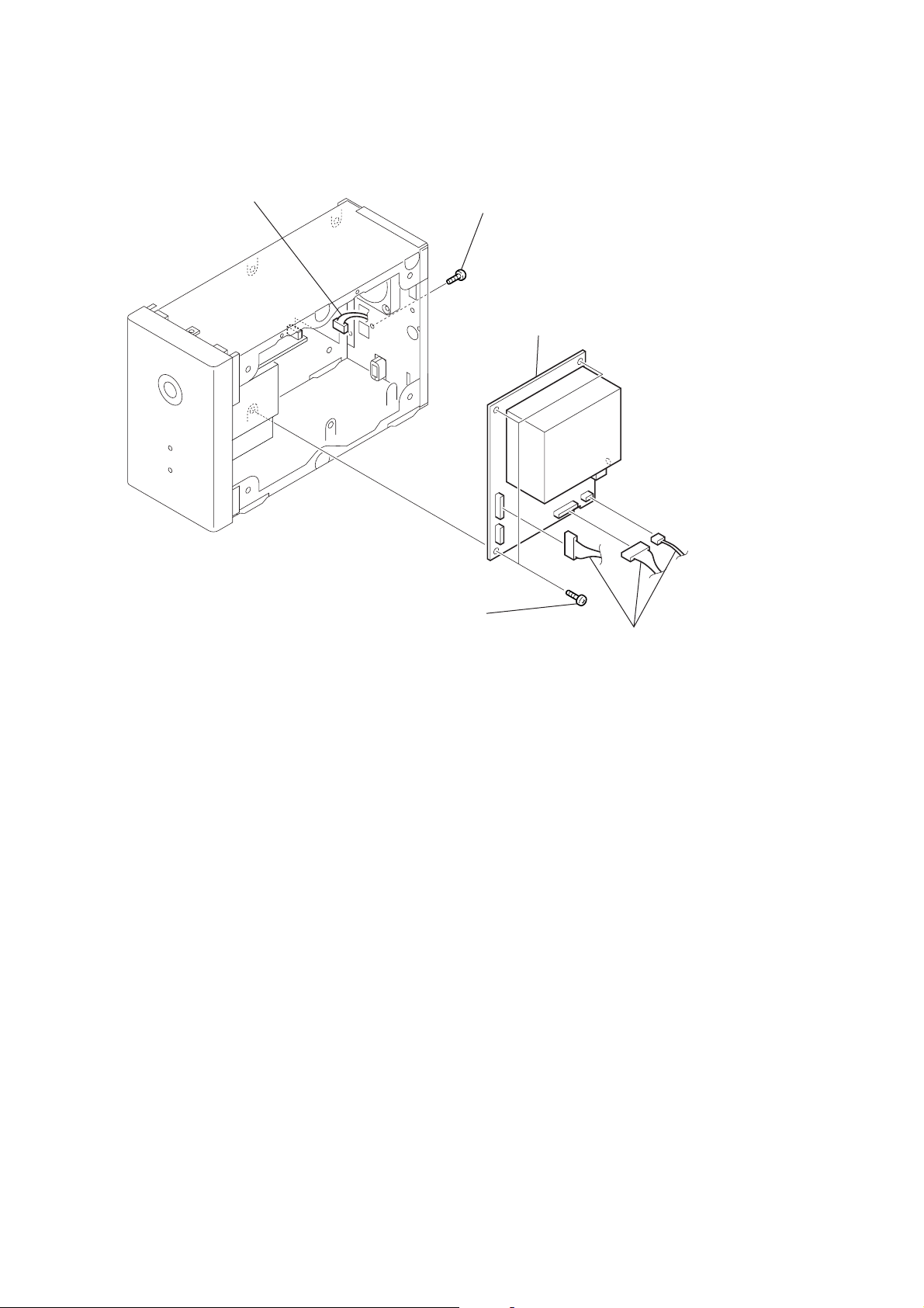
2-2. CASE (REAR AMPLIFIER)
2
1
four flat head screws
2
case (rear amplifier)
3
1
four flat head screws
4
Page 5
2-3. VS BOARD
t
2
screw
(BVTP 3
×
8)
3
RX board
1
wire (flat type) (17 core)
(CN7403)
2
screw
(BVTP 3
×
8)
2
two screws
(BVTP 3
×
8)
4
insulation shee
TA-FLX9W
2-4. RX BOARD
3
VS board
(except Thai model)
1
connector
(CN972)
1
connector
(CN971)
5
Page 6
TA-FLX9W
2-5. MAIN BOARD
1
connector
(CN903)
2
screw
(BVTP 3
×
8)
3
MAIN board
2
three screws
(BVTP 3
×
8)
1
three connectors
(CN102, CN104, CN105)
6
Page 7
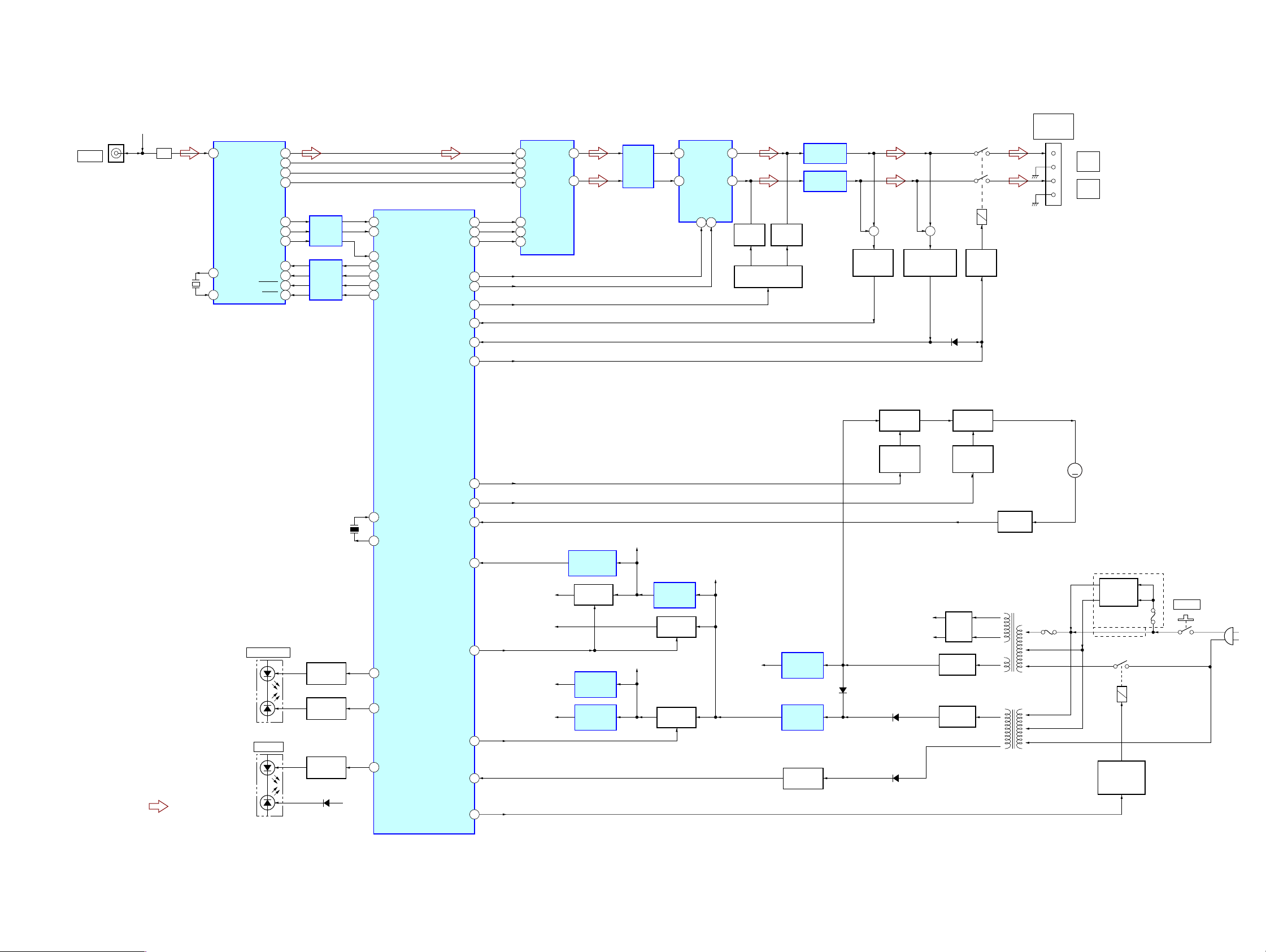
3-1. BLOCK DIAGRAM
TA-FLX9W
SECTION 3
DIAGRAMS
J7401
DIR-R1
IF +5V
LPF
X7401
12.288MHz
RF DEMODULATOR,
A/D CONVERTER
10
ADVIN
OSCO
4043OSCI
IC7402
DAOUT
LRCK
BCK
APX
CSOD
DTVALID
SRDT
SWDT
SCLK
XSCEN
XRST
TM101
SPEAKERS
IC7407
D/A CONVERTER
60
59
54
31
IC7405
REAR AMP CONTROLLER
33
61
34
35
37
36
13
IC7411
LEVEL
SHIFT
IC7410
LEVEL
SHIFT
16 CSOD
14 DTVALID
53 DIAT_SRDT
52 DIAT_SWDT
51 DIAT_CK
54 XSCEN
28 XRST
DAC_DATA
DAC_CLK
DAC_LAT
VOLIC_DATA
VOLIC_CLK
MUTE
FANON
PROTECT
SPRY
26
25
27
34
33
41
45
15
31
2
DATA
3
LRCK
1
BCK
16
SCK
13
MD
14
MC
15
ML
VOL
VOR
7
8
IC7408
LINE
AMP
IC7409
ELECTRICAL VOLUME
1
VIN1
VOUT1
8
VIN2
VOUT2
DATA
CLOCK
4
5
2
7
MUTING
Q7406
MUTING CONTROL
Q7403, 7411
MUTING
Q7405
IC101
POWER AMP
IC102
POWER AMP
+
LEVEL
DETECT
Q108, 109
B+ SWITCH
Q112
+
OVER CURRENT
DETECT
Q105 – 107
D102
REGULATOR
Q113
-1
-2
RELAY
DRIVE
Q104
RY101
IMPEDANCE
USE 8Ω
(+)
REAR
L
(–)
(+)
REAR
R
(–)
• SIGNAL PATH
: AUDIO
D201
ON/STANDBY
D202
ON LINE
X7402
12.5MHz
LED DRIVE
Q101
LED DRIVE
Q102
LED DRIVE
Q103
D114
+6V
22
23
38
36
37
X0
X1
LED_ON
LED_RED
LED_DIAT
FAN1
FAN2
RST
STOP
FAN MOTOR
DRIVE
Q110
42
43
44FAN_CLK
+3.3V
19
D/A B+
E.VOL B+
47PSAVE
+1.5V
+2.5V
39DIAT_OFF
32
35PWR_RY
RESET SIGNAL
GENERATOR
IC7403
B+ SWITCH
Q7401, 7402
+1.5V
REGULATOR
IC7404
+2.5V
REGULATOR
IC7401
IF +5V
+3.3V
REGULATOR
IC7406
B+ SWITCH
Q7407, 7408
B+ SWITCH
Q7409, 7410
+5V
+6V
+6V
REGULATOR
IC103
+5V
REGULATOR
IC104
AC DETECT
Q901
D111
POWER AMP
POWER AMP
D110
D906, 907
B+
B–
FAN MOTOR
Q111, 117
RECT
D104
RECT
D106 – 109
RECT
D902 – 905
DRIVE
PROTECT
POWER TRANSFORMER
(MAIN)
POWER TRANSFORMER
(SUB)
Q114
T901
T902
F901
M101
MM
(FAN)
(EXCEPT Thai model)
VOLTAGE
SELECTOR
(Thai model)
MAIN POWER
RELAY DRIVE
S971
RY901
ON/OFF
Q902
F971
S951
POWER
(AC IN)
TA-FLX9W
77
Page 8
TA-FLX9W
• Note for Printed Wiring Boards and Schematic Diagrams
Note on Printed Wiring Boards:
• X : parts extracted from the component side.
• Y : parts extracted from the conductor side.
f
•
• : Pattern from the side which enables seeing.
(The other layers' patterns are not indicated.)
Caution:
Pattern face side: Parts on the pattern face side seen from
(Conductor Side) the pattern face are indicated.
Parts face side: Parts on the parts face side seen from
(Component Side) the parts face are indicated.
• Indication of transistor.
: internal component.
C
Q
B
E
These are omitted.
Note on Schematic Diagram:
• All capacitors are in µF unless otherwise noted. (p: pF)
50 WV or less are not indicated except for electrolytics
and tantalums.
• All resistors are in Ω and 1/
specified.
• f : internal component.
• 2 : nonflammable resistor.
• C : panel designation.
Note: The components identified by mark 0 or dotted line
with mark 0 are critical for safety.
Replace only with part number specified.
• A : B+ Line.
• B : B– Line.
• Voltages and waveforms are dc with respect to ground
under no-signal (detuned) conditions.
Note: When mesurering voltages and waveforms, con-
nect with HCD-FLX9W (states: tuner).
no mark : TUNER
∗ : Impossible to measure
• Voltages are taken with a VOM (Input impedance 10 MΩ).
Voltage variations may be noted due to normal production tolerances.
• Waveforms are taken with a oscilloscope.
Voltage variations may be noted due to normal production tolerances.
• Circled numbers refer to waveforms.
• Signal path.
F : AUDIO
• Abbreviation
TH : Thai model
4
W or less unless otherwise
• Circuit Board Location
PSW board
LED board
STBY board
MAIN board
VS board
(EXCEPT Thai)
RX board
• Waveforms
– RX Board –
IC7402 rd (OSCO)
1
1 V/DIV, 50 ns/DIV
IC7405 wd (X1)
2
1 V/DIV, 50 ns/DIV
2.9Vp-p
81 ns
3.3 Vp-p
80.5 ns
TA-FLX9W
88
Page 9

TA-FLX9W
3-2. PRINTED WIRING BOARD – RX Board –
1 2 3 4 5 6 7 8
A
B
C
RX BOARD
IC7401
4
6
D
E
(COMPONENT SIDE)
R7403
C7407
R7491
C7405
R7492
C7444
C7409
C7406
3
1
R7401
L7401
Q7409
R7477
R7404
E
R7478
R7405
C7418
C7415
R7489
R7426
R7425
R7427
IC7402
C7420
C7425
L7404
54
13
C7437
X7401
R7428
R7417
L7406
IC7404
C7436
R7430
R7482
R7444
R7409
C7457
Q7402
R7429
C7468
• See page 8 for Circuit Boards Location.
16 9
1
E
1
16
31
45
IC7407
8
C7439
R7474
R7475
R7459
IC7403
R7486
R7483
R7476
R7422
IC7405
R7484
R7501
4964
3217
R7431
R7450
R7448
48
33
L7407
IC7410
1
7
R7451
R7456
R7435
R7436
C7469
R7437
R7494
14
R7449
R7447
8
R7503
R7493
R7438
R7433
C7470
C7447
R7442
R7485
R7487
R7439
R7499
R7472
R7440
R7497
E
5
8
IC7408
IC7409
1
4
Q7411
Q7408
R7473
:Uses unleaded solder.
R7443C7445
R7441
C7446
C7448
4
R7498
R7500
8
5
R7470
R7466
R7465
EE E
Q7405
Q7406
E
Q7407
R7469
• Semiconductor
Location
Ref. No. Location
D7401 H-4
D7402 J-4
D7403 K-7
D7404 I-3
IC7401 C-2
IC7402 B-3
IC7403 E-4
IC7404 D-3
IC7405 D-5
IC7406 K-6
IC7407 A-4
IC7408 B-7
IC7409 C-7
IC7410 B-6
IC7411 G-6
Q7401 H-5
Q7402 B-4
Q7403 J-2
Q7405 D-7
Q7406 D-7
Q7407 E-7
Q7408 D-7
Q7409 E-2
Q7410 K-7
Q7411 D-7
1-864-776-11(11)
F
RX BOARD
G
H
C7451
C7453
I
R7463 R7462
J
R7446
K
(CONDUCTOR SIDE)
C7449
R7502
C7454
E
Q7403
R7488
R7445
1
2
C7450
C7452
CN7402
(FOR CHECK)
C7455
C7456
R7460
R7452
CN7403
R7453
R7455
R7454
R7432
D7404
C7464
R7495
17
C7466
R7479
C7442
C7462
C7463
Q7401
C7433
C7441
X7402
17
16
R7424
R7420
R7457
R7421
D7402
C7458
R7496
D7401
R7418
R7434
R7458
R7419
R7415
R7414
E
R7406
C7426
C7423
R7423
R7412
R7410
C7429
C7432
C7434
C7416
C7435
C7465
C7440
C7430
C7467
C7461
C7460
R7407
C7419
3
IC7406
IC7411
8
14
C7421
R7408
2
C7459
1
C7424
C7431
C7422
C7428
7
1
C7417
C7438
Q7410
C7404
C7427
FB7401
C7410
C7408
L7402
C7403
R7490
C7414
C7413
R7402
E
D7403
C7412
C7401
C7411
C7402
C7443
R7480
1-864-776-
J7401
DIR-R1
11
(11)
TA-FLX9W
A
MAIN BOARD
CN101
(Page 13)
(CHASSIS)
99
Page 10

TA-FLX9W
3-3. SCHEMATIC DIAGRAM – RX Board (1/2) –
(1/2)
C7401
(CHASSIS)
J7401
DIR-R1
0.1
C7402
47
10V
L7401
47µH
R7480
2.2
L7402
10µH
C7405
0.1
C7403
10V
C7407
R7403
FB7401
R7491
R7492
4
0
1
4
.0
7
0
C
2
0
0
4
2
7
2
R
1P
B
.8
6
3
7
0
4
-1
7
E
T
D
S
Z
D
U
C7443
0.1
R7401
10k
C7406
0.01
C7412
0.1
C7411
47
10V
C7421
0.1
C7408
0.1
47
C7410
1
68
4.7k
2.2k
9
0
1
4
.0
7
0
C
0
9
k
4
.7
7
4
R
0.1
XRST2
C7467
100p
R7487
100
+2.5V REGULATOR
IC7401
TK11225CMCL
CNT
GND
CNP
GND
OUT
C7444
• See page 15 for IC Block Diagrams. • See page 8 for Waveform.
Q7409,7410
B+ SWITCH
C7414
C7413
47
0.1
10V
+1.5V REGULATOR
IN
LRCK
DATA
LID2
R7489
100
DTVALID
APVCI
C7420
DAOUT
VSS
5
0
k
4
7
3.3
R
4
0
0
4
7
82
R
8
1
0.1
74
C
0.1
VDDI
LRCK
RF DEMODULATOR,
A/D CONVERTER
CXD4017R
APAVD
APCPO
L7404
0.1
10µH
MST
XSM
SMCK
VDDE
VSS
ADVRH
ADAVS
ADAVD
ADVRL
ADVIN
VDDE
VSS
XRST
DIFM0
DIFM1
DTSEL
PLREF
XTST
EMPFS0
EMPFS1
TESTMD
PLVAR
1
2
R
F
0
0
E
A
4
R
V
7
74
L
L
P
P
JL
JL
C7415
0.01
C7417
47
10V
IC7402
2
2
74
C
VSS
APAVS
0.1
IC7404
S-T111B15
MC-0GATFG
VIN
VOUT
VDDE
VSS
C7425
TXOUT
VDDI
C7428
C7427
47
0.1
10V
Q7409
2SA1162G-TE85L
R7477
2.2k
R7408
ICLK
VCOR
C7419
47
10V
SYMCLK
CHNUM
TEST7
DIVCODE
C7431
0.1
TEST6
APX
SCK
10k
C7416 C7424
0.1 0.1
TEST5
TEST4
TEST3
TEST2
TEST1
TEST0
OSCO
VSS
VDDE
OSCI
VSS
SCMODE
SCLK
XSCEN
SWDT
SRDT
CSOD
EXTCK
Q7410
RT1N141C
CE
VSS
NC
0.1
BCK
BCK/RCLK
VDDE
0p
0
1
9
5
4
7
C
+3.3V REGULATOR
µPC2933T-E2
p
0
0p
0
0
1
1
0
1
6
6
4
4
7
7
C
C
R7478
10k
IC7406
C7433 C7434
15p 15p
X7401
12.288MHz
R7485
100
R7486
100
R7483
100
R7429
100
R7482
100
I
O
SCLK2
XSCEN2
SWDT2
SRDT2
CSOD2
C7442
100
10V
C7437
0.1
C7438
47
10V
G
C7436
C7435
0.1
47
10V
D/A CONVERTER
PCM1751DBQR
IC7407
C7439
R7423
10k
Q7401,7402
B+ SWITCH
R7428
0.1
MC
MD
ML
SCK
220
R7441 C7448 R7498 R7500
0
2
20
20
2
2
2
7
5
6
2
2
2
4
4
4
7
7
7
R
R
R
LRCK
DATA
BCK
C7440
47
10V
2SA1162G-TE85L
R7430
2.2k
Q7402 IC7409
RT1N141C M62429P
C7441
L7407
C7463
47
0.1
10V
C7462
0.1
Q7401
R7502
C7470
C7469
C7450
1
1
10
10
50V
4.7k 2200p 15k 10k
2
VIN
1
VIN
R7439
R7438
1.8k
1.8k
2
T
U
O
V
1
T
U
VO
R7443
1.8k
R7440 C7447 R7497 R7499
4.7k 2200p 15k 10k
R7442
1.8k
C7446 C7445
2200p 2200p
C7454
470
6.3V
C
C
CK
V
LO
C
A
D
T
N
A
G
D
ELECTRICAL
VOLUME
Q7408
RT1N141C
C7453
10
50V
R7466
R7465
C7452
10
R7462
50V
Q7403,7411
MUTING CONTROL
R7472
10k
10k
1k
DTA124EKA
2.2k
Q7403
IC7408(1/2)
TLV23621DR
IC7408(2/2)
TLV23621DR
6
5
R7469R7463
10k1k
Q7407
2SA1162G-TE85L
832
1
7
4
R7470
10k
Q7407,7408
LINE AMP
Q7405,7406
C7455
0.1
B+ SWITCH
2SD1938(F)-S
MUTING
2SD1938(F)-S
Q7406
Q7405
R7473
Q7411
DTA124EKA
C7456
100
10V
10k
C7449
47
10V
C7451
10
50V
R7488
10k
TA-FLX9W
3
1
1
A
A
A
3
2
6
5
4
A
A
A
A
A
A
9
8
7
2
1
1
10
A1
A
A
A
(Page 11)
1010
Page 11

TA-FLX9W
3-4. SCHEMATIC DIAGRAM – RX Board (2/2) –
(2/2)
C7465
0.1
C7429
100
10V
R7444
IC7403
G8ZT2G
R7409
R7445
R7407
R7459
R7421
C7458
100p
100
10k
100
R7496
10k
100
100
100
C7468
C7423 R7406
0.01 10k
0.1
C7457
0.1
R7410
L7406
10µH
10k
LID
PROTECT
CSOD
RESET SIGNAL GENERATOR
S-80829CNMC-
• See page 8 for Waveform. • See page 17 for IC Pin Function Description.
A1
A2
A3
R7417
10k
R7432
NC
MOD2
VOLT
TEMP
NC
NC
NC
NC
NC
NC
AVCC
AVR
AVSS
DTVALID
PROTECT
CSOD
C7426
0.1
C7432
2
R7412
R7434
D7402
1SS352
T2
SCK2
SIN
SO
100
100
100
R7475
R7474
R7476
R7415
10k
2
2
2
3
C
T
N
IN
T2
O
S
S
IN
0
D
T
O
C
S
C
M
N
R
N
1k
100
1
D
ESET
M
R
R7414R7411
10k10k
C
R
K
E
N
C
_V
S
D
O
M
REAR AMP CONTROL
MB89537APFM-G
-598-BNDE1
1
D
O
1
0
X
X
M
X7402
12.5MHz
L
E
_S
H
C
IC7405
S
S
V
100
R7419
C
M
C
C
V
LK
C
_
C
A
D
10k
0.01
100
R7418
D
M
DT
DT
CK
SW
SR
XSCEN
100
100
100
100
P10
R7446
100
D7401
1SS352
R7493
10k
R7494 R7503
10k 10k
D7404
R7451
R7456
R7437
R7455
R7454
R7453
R7452
UDZSTE-172.7B
R7479
R7450
R7449
R7448
R7447
R7435
R7436
100
100
100
100
FANON
100
FANCLK
100
100
100
100
LED_ON
100
LED_DIAT
100
LED_RED
100
PWRRY
100
100
R7422
R7424
R7484
R7431
C7464
100p
E
T
T
C
N
E
D
N
C
R
S
S
X
T_
IA
D
TA
T
A
LA
D
T
_
_
S
C
C
A
A
R
X
D
D
100
100
R7420
R7433
XRST
L
M
K
D
C
W
T_
IA
_S
T
D
IA
D
2
0
G
P
23
P
P
100
R7457
Y
SPR
C
T
N
U
M
W
PWR_CTL
P
PSAVE
SCMODE
FAN_ON
FAN_CLK
FAN2
FAN1
MUTE
DIATOFF
LED_ON
LED_DIAT
LED_RED
PWR_RY
VOLIC_DATA
VOLIC_CLK
Y
P
R
TO
P
S
S
100
R7458
P
STO
R7501 R7495
10k 10k
FAN2
FAN1
100
R7460
(Page 10)
A4
A5
A6
A7
A8
A9
SWDT2
CSOD2
CSOD
SRDT2
SRDT
XSCEN
XSCEN2
SWDT
LEVEL SHIFT
IC7411
SN74HCT08APWR
LEVEL SHIFT
IC7410
SN74LV08APWR
C7430
SCLK2
LID2
LID
0.1
CK
XRST
XRST2
C7466
A10
A11
A12
A13
CN7403
17P
PROTECT
LED_ON
LED_RED
LED_DIAT
PWRRY
STOP
SPRY
FANON
FANCLK
FAN2
FAN1
0.1
MD1
SCK2
RESET
SIN2
SOT2
PROTECT
LED_ON
LED_RED
LED_DIAT
PWRRY
FANON
FANCLK
CN7402
RESET
L-CH
R-CH
STOP
SPRY
FAN2
FAN1
SCK2
SOT2
GND
GND
+5V
GND
(Page 14)
7P
MD1
GND
VDD
SIN2
(FOR CHECK)
TA-FLX9W
1111
Page 12

TA-FLX9W
• Semiconductor
Location
Ref. No. Location
D101 D-8
D102 I-8
D103 I-8
D104 D-3
D105 K-2
D106 H-3
D107 H-3
D108 G-2
D109 G-3
D110 B-2
D111 C-2
D112 B-9
D113 C-8
D114 C-8
D201 D-12
D202 C-12
IC101 K-5
IC102 F-6
IC103 H-2
IC104 B-3
Q101 B-8
Q102 B-6
Q103 B-7
Q104 G-8
Q105 H-8
Q106 G-8
Q107 H-8
Q108 K-2
Q109 K-2
Q110 B-8
Q111 B-9
Q112 A-9
Q113 B-10
Q114 B-8
Q117 B-9
3-5. PRINTED WIRING BOARDS – MAIN Section –
1 2 3 4 5 6 7 8 9 10 11 12
A
B
MAIN BOARD LED BOARD
1
CN103
1
D110
C141
3
IC104
C143
B
STBY
BOARD
C
D
E
F
G
H
I
CN903
(Page 13)
C
POWER
TRANSFORMER
(MAIN)
T901
(Page 13)
IC103
4
D111
CN102
1
5
THP101
C130
C132
13
C134
C127
C126
JW141
C136
JW118
D108
JW140
C131
D107
D104
JW134
JW117
D109
JW133
JW146
C128
C174
C129
JW130
JW137
JW138
D106
JW145
JW147
JW154
JW151
• See page 8 for Circuit Boards Location.
RX BOARD
(Page 9)
CN7403
R155
R156
R154
E
JW109
C117
R136
R127
C116
R105
JW108
R103
-2
-1
R128
Q102
R102
R126
R104
JW116
JW111
JW112
L102
R133
JW119
R130
R134
R131
JW125
1
IC102
210
C142
JW139
JW123
JW132
R108
JW157
C145
C123
C122
JW114
JW122
C120
C121
A
CN101
JW115
C124
JW126
R116
:Uses unleaded solder.
Q110
EE
Q103
CN104
RY101
C115
JW128
C118
D114
Q101
R107
C111
R121
Q106
E
JW127
Q105
E
JW136
JW143
JW144
R106
15
JW107
JW104
R129
11
JW129
R101
R132
R123
D103
JW105
JW106
D101
JW121JW124
Q104
JW120
Q107
E
R122
Q114
D113
E
E
E
R153
C112
R124
D102
R157
JW103
R119
JW101
R120
R151
R152
Q112
R150
E
C175
D112
FB101
Q113
E
R148
C133
JW102
1
M101
M
(FAN)
3
+
REAR
R
–
TM101
SPEAKERS
IMPEDANCE
USE 8Ω
+
REAR
L
–
D202
ON LINE
D201
ON/STANDBY
CN201
5
1
1-862-759-12(12)
E
Q111
Q117
E
1
3
CN105
R137
C125
C153
C113
R125
TA-FLX9W
JW148
R114
J
JW155
R144
R146
C140
R140
R141
Q109
K
C139
E
C138
R143
L
R142
JW150
D105
Q108
C137
E
C108
R147
R145
C107
C106
JW158
C109
C103
C144
R109
C101
R111
R110
JW153
C102
JW152
C104
R117
IC101
JW156
C150
210
111
R112
C110
R113
L101
R115
1-862-757-12(12)
1212
Page 13

TA-FLX9W
3-6. PRINTED WIRING BOARDS – POWER SUPPLY Section –
1 2 3 4 5 6
STBY BOARD
A
(CHASSIS)
W901
D904
D902 D903
JW903
D905
D907
D906
JW902
C902
C901
T902
POWER
TRANSFORMER
(SUB)
B
C903
• See page 8 for Circuit Boards Location.
1
(TH)
JW991
5
CN901
:Uses unleaded solder.
VS BOARD
S971
VOLTAGE SELECTOR
220V – 240V
110V – 120V
(E15, SP)
220V – 240V
120V – 127V
(EA)
-1 -2
JW971
CN972
5
1
(EXCEPT TH)
FH972
F971
FH971
• Semiconductor
Location
Ref. No. Location
D901 C-2
D902 B-1
D903 B-2
D904 A-1
D905 A-2
D906 B-2
D907 A-2
D908 B-2
Q901 C-2
Q902 C-2
C
D
B
MAIN
BOARD
CN103
(Page 12)
R904
C904
4
1
R906
CN903
R905
TP901
Q901
R902
JW904
JW901
E
D908
D901
E
R901
Q902
T901
POWER
TRANSFORMER
(MAIN)
RY901
13
CN902
1
F901
FH901 FH902
1-862-758-
5
C
MAIN BOARD
CN102
(Page 12)
12
(12)
(TH)
15
PSW BOARD
CN971
1
12
CN952
2
S951
POWER
12
12
1-862-794-
(12)
TA-FLX9W
E
CN951
12
1-862-760-
(12)
(AC IN)
1313
Page 14

TA-FLX9W
3-7. SCHEMATIC DIAGRAM – MAIN Section –
C102
10
R108
50V100
CN101
17P
PROTECT
LED_ON
LED_RED
LED_DIAT
GND
L-CH
GND
R-CH
+5V
GND
PWRRY
(Page 11)
STOP
SPRY
FANON
FANCLK
FAN2
FAN1
100
100
100
R156
R155
R154
L101
POWER AMP
IC101
MUTE
GND
NC
V+
V-
NC
V+
R117
R109C101
100k1000p
C103
100
C144
4700p
C145
C115
4700p
10
R126
50V100
R127C116
100k1000p
C117
100
16V
R140C140
100k4.7
16V
V+
Q109 Q108
2SC2712 2SC2712
C139 R141 C138 R143
R110
R111
470
V-
NC
R128R129
680470
D105
1SS355
Q108,109
LEVEL
DETECT
13.3k1 820
680
NC
V+
R142 R144
10k 4.7k
33k
R112
100k
MUTE
GND
R136
33k
R130
100k
NC
LM3886T
C106
C104
10
220p
50V
C107
10
50V
POWER AMP
IC102
NC
LM3886T
C120
C118
10
220p
50V
C121
10
50V
R146
C137
220k
10
50V
R145 R147
68k 100k
C128
C108
3300
0.047
0.047
0.047
0.047
50V
C129
C109
3300
50V
C122
C123
R113
R131
D104
RBV-402
10
C150
0.047
C124
0.047
C174
0.047
10
C127 C126
0.1
100V
-01
0.6µH
-1
R115
4.7
R116
27k
C110
0.047
R114
47k
R132
47k
L102
0.6µH
R133
4.7
R134
27k
0.1
100V
R157R151
2.2k10k
-2
RY101
D101
1SS355
R119
10
RELAY DRIVE
C111
220
10V
Q105-107
OVER CURRENT
R122 R123
10k 10k
C112 R124
0.1 33k
B+ SWITCH
Q110
DTC124EKA
FAN MOTOR
DRIVE
DTC124EKA
DETECT
UDZSTE-175.6B
Q117
2SD1938
R121
47k
Q104
2SC27122SA1162
2SC2712
D112
DTC124EKA
Q105Q106
Q107
R148
1.5k
Q111
Q111,117
FAN MOTOR
DRIVE
R120 R153
4.7k 1k
D103
D102
1SS355
RB551V
Q113R150Q112
2SD166410k2SB1132
REGULATOR
C133
10
50V
Q114
DTC124EKA
PROTECT
D113
UDZS-2.7B
R125
10
C113
0.047
C153
0.047
C175
0.047
C125
0.047
R137
10
FB101
CN105
R152
1k
3P
(CHASSIS)
REAR
L
TM101
SPEAKERS
IMPEDANCE
USE 8Ω
REAR
R
M101
(FAN)
T901
POWER TRANSFORMER
PWR_RLY
STOP
STANBY_PWR
DGND
(MAIN)
F901
T630mAL
250V
CN902
3P
R902
4.7k
R901
47k
RELAY DRIVE
2SC2712 10k
AC DETECT
CN971
2P
Q902
2SC2712
MAIN POWER
ON/OFF
Q901 R906
C903
4700
16V
C904
R905
1
33k
50V
R904
D907
47k
1SS355
F971
T1.25AL
250V
CN903CN103
4P4P
(EXCEPT TH)
(TH)
CN952CN951
2P2P
D908D901
1SS3551SS355
EC10QS04
EC10QS04
EC10QS04
EC10QS04
1SS355
RY901
D902
D903
D904
D905
D906
-1
-2
C902
0.01
C901
0.01
T902
POWER
TRANSFORMER
(SUB)
S971
VOLTAGE SELECTOR
120V 220V 240V110V
CN901
5P
220V 240V120V 127V
(E15,SP)
(EA)
JW991
(TH)
W901
(CHASSIS)
CN972
5P
CN102
POWER
5P
S951
D109
1SR154
2SA1162
R101 R107R104
470 4701k
Q101
2SC2712
Q103
D114
1SS355
C142
100
16V
CN104
5P
ON
ERR
RDY
GND
STBY
CN201
5P
+6V REGULATOR
IC103
NJM78L06AT3
OGI
C134 C136
4.7 0.1
OGI
IC104C143
NJM78M05FA0.1
+5V REGULATOR
C132
1000
16V
D110D111
C141
100
16V
RB551VRB551V
1SR154
1SR154
1SR154
C130
D108
0.01
D106
C131
0.01
D107
THP101
(AC IN)
R102
1k
Q101-103
LED DRIVE
R103
1k
2SC2712
R105
4.7k
Q102
D201 D202
SML72420C-TP15 SML72420C-TP15
ON/STANDBY ON LINE
R106
10k
TA-FLX9W
The components identified by mark 0 or dotted
line with mark 0 are critical for safety.
Replace only with part number specified.
1414
Page 15

• IC Block Diagrams
– RX Board –
IC7401 TK11225CMCL-G
VIN
6 4
CONTROL
CIRCUIT
BANDGAP
REFERENCE
1 2 3
CONT
CONSTANT
CURRENT
SOURCE
GND
5
GND
OVER HEAT &
OVER CURRENT
PROTECT
VOUT
NP
IC7404 S-T111B15MC-OGATFG
ON/OFF
VSS
1
ON/OFF
CIRCUIT
2
NC
3
OVER CURRENT
PROTECTOR
REFERENCE
VOLTAGE CIRCUIT
TA-FLX9W
+
–
5
VIN
VOUT
4
IC7402 CXD4017R
TEST12 1
TEST13 2
TEST14
VDDE
VSS 5
ADVRH 6
ADAVS 7
ADAVD 8
ADVRL 9
ADVIN 10
VDDEE 11
VSS
XRST
DIFM0 14
DIFM1 15
TEST15 16
3
4
12
13
BUFFER
RAM
A/D
CONVERTER
17
DEMODULATOR
19
18
PLREF
PLVAR
TEST1164EMPFS163EMPFS062DTVALID61DAOUT60LRCK59VDDI58VSS57VDDE56BCK
OUTPUT
INTERFACE
PLL
SELECTOR
20
21
23
24
25
VSS
TEST16
APVCI
APAVS
APCPO22APAVD
CLOCK
26
VSS
TEST1055TEST953TEST852TEST751TEST650TEST5
54
ERROR
CORRECTOR
27
28
29
VDDI
VDDE
VCOR
CHNUM
30
DIVCODE
31
APX
49
CLOCK
GENERATOR
CONTROLLER
32
EXTCK
TEST448
TEST347
TEST246
TEST145
TEST044
OSCO43
42
VSS
41
VDDE
OSCI40
VSS39
SCMODE38
SCLK37
XSCEN36
SWDT35
SRDT34
CSOD33
15
Page 16

TA-FLX9W
IC7407 PCM1751DBQR
SCK
16
SYSTEM
CLOCK
MANAGER
SYSTEM
CLOCK
ML
MC
15
14
13
FUNCTION
CONTROL
INTERFACE
SERIAL
INPUT
INTERFACE
1 2 3
BCK
DATA
MD
LRCK
ZEROL
12
11
ZERO DETECT
8 TIME OVER
SAMPLING
DIGITAL FILTER
WITH
FUNCTION
CONTROLLER
ZEROR
ENHANCED
MULTI-LEVEL
DELTA-SIGMA
MODULATOR
D/A
CONVERTER
D/A
CONVERTER
POWER SUPPLY
DGND
OUTPUT AMP AND
LOW-PASS FILTER
OUTPUT AMP AND
LOW-PASS FILTER
VCC
VDD
10
7 84 5 6
VCOM
VOUTL
AGND
9
VOUTR
IC7409 M62429FP-TP
VR1
VR2
VIN2
8
VOL AMP 2
VOL AMP 1
1
VIN1
VOUT2
7
+
–
REF AMP
+
–
–
+
2
VOUT1
VREF
VCC
6
3
GND
CLOCK
5
LOGIC
CONTROL
4
DATA
16
Page 17

• IC Pin Function Description
RX BOARD IC7405 MB89537APFM-G-598-BNDE1 (REAR AMP CONTROLLER)
TA-FLX9W
Pin No.
1NCONot used
2MOD2ISetting terminal for the CPU operation mode Fixed at “L” in this set
3VOLT
4 TEMP
5 to 10 NC
11
12 AVR
13 AVSS
14 DTVAILD
15 PROTECT
16 CSOD
17, 18 NC
19 RST
20, 21 MD0, MD1
22 X0
23
24 VSS
25 DAC_CLK
26 DAC_DATA
27 DAC_LAT
28 XRST
29 P23
30
31 SPRY
32 STOP
33
34
35
36
37
38
39
40
41 MUTE O
42
43
44
45
46
47
48
49
50
51 DIAT_CK
Pin Name
AVCC
X1
PPG02
VOLIC_DATA
VOLIC_CLK
PWR_RY
LED_RED
LED_DIAT
LED_ON
DIATOFF
P10
FAN1 O Fan motor drive control signal output terminal “H”: active
FAN2 O Fan motor drive speed control signal output terminal “H”: high speed, “L”: low speed
FAN_CLK I Fan motor stop detection signal input terminal “L”: fan motor stop
FANON I Output level detection signal input terminal “H”: low level, “L”: high level
SCMODE
PSAVE
PWR_CTL
NC
PWMUTE
I/O Description
I
Battery voltage detection input terminal Not used
I
Battery thermal detection input terminal Not used
—
Not used
—
Power supply terminal (+3.3V) (for A/D converter)
I
Reference voltage (+3.3V) input terminal (for A/D converter)
—
Ground terminal (for A/D converter)
I
Data valid flag input from the RF demodulator “L”: invalid, “H”: valid
I
Over current detection signal input for speaker output terminal “L”: over current
I
Captor start delay signal input from the RF demodulator “H” active
—
Not used
Reset signal input terminal “L”: reset
I
For several hundreds msec. after the power supply rises, “L” is input, then it changes to “H”
I
CPU operation mode setting signal input terminal
I
Main system clock input terminal (12.5 MHz)
O
Main system clock output terminal (12.5 MHz)
—
Ground terminal
O
Serial data transfer clock signal output to the D/A converter
O
Serial data output to the D/A converter
O
Serial data latch pulse signal output to the D/A converter
O
Reset signal output to the RF demodulator and stream processor “L”: reset
I
Setting terminal for the CPU operation mode Fixed at “L” in this set
I
Setting terminal for the CPU operation mode Fixed at “H” in this set
O
Speakers on/off relay drive signal output “H”: speakers on
I
Power failure detection input terminal “L”: power on
O
Serial data output to the electrical volume
O
Serial data transfer clock signal output to the electrical volume
O
Main power on/off relay drive signal output terminal “H”: power on
O
LED drive signal output of the standby indicator “H”: LED on
O
LED drive signal output of the DIAT signal receive state indicator “H”: LED on (receive error)
O
LED drive signal output of the power on indicator “H”: LED on
O
Power on/off control signal output terminal for the DIAT circuit “H”: active
I
Setting terminal for the CPU operation mode Fixed at “H” in this set
Muting on/off control signal output terminal “L”: muting on
O
Control mode selection signal output terminal “L”: pin setting, “H”: serial setting Not used
O
Power on/off control signal output terminal for the volume control circuit “H”: active
O
Not used
—
Not used
O
Not used
O
Serial interface data clock signal output to the RF demodulator
17
Page 18

TA-FLX9W
Pin No.
52 DIAT_SWDT
53
54
55 NC
56 VCC
57 CH_SEL
58 MOD_VER I Model destination setting terminal “H”: AC model, “L”: battery model
59 NC
60 SCK2
61 SOT2
62 SIN2
63 INT23
64 NC
Pin Name
DIAT_SRDT
XSCEN
I/O Description
O
Serial interface data write signal output to the RF demodulator
I
Serial interface data read signal input from the RF demodulator
O
Serial interface enable signal output to the RF demodulator
—
Not used
—
Power supply terminal (+3.3V)
I
Not used
—
Not used
—
Not used
—
Not used
—
Not used
I
Not used
—
Not used
18
Page 19

SECTION 4
EXPLODED VIEWS
TA-FLX9W
NOTE:
• -XX and -X mean standardized parts, so they
may have some difference from the original
one.
• Color Indication of Appearance Parts
Example:
KNOB, BALANCE (WHITE) . . . (RED)
•Abbreviation
E15 : Iranian model
EA : Saudi Arabia model
↑↑
Parts Color Cabinet's Color
SP : Singapore model
TH : Thai model
4-1. FRONT PANEL SECTION
• Items marked “*” are not stocked since they
are seldom required for routine service. Some
delay should be anticipated when ordering
these items.
• The mechanical parts with no reference
number in the exploded views are not supplied.
• Accessories are given in the last of the
electrical parts list.
5
The components identified by mark
0 or dotted line with mark 0 are
critical for safety.
Replace only with part number
specified.
6
5
not supplied
(PSW board)
4
not supplied
#3
#1
not supplied
2
not supplied
(LED board)
chassis section
4
4
1
#1
Ref. No. Part No. Description Remark
1 X-4956-474-1 PANEL ASSY, FRONT (REAR AMP)
24-255-371-01 BUTTON (POWER, REAR AMP)
44-951-620-01 SCREW (2.6X8), +BVTP
54-227-843-31 SCREW (TP), FLAT HEAD
Ref. No. Part No. Description Remark
6 4-255-374-11 CASE (REAR AMPLIFIER)
#1 7-685-646-79 SCREW +BVTP 3X8 TYPE2 IT-3
#3 7-685-871-01 SCREW +BVTT 3X6 (S)
19
Page 20

TA-FLX9W
4-2. CHASSIS SECTION
F901
56
#1
#1
not supplied
#1
#1
not supplied
not supplied
55
(EXCEPT TH)
not supplied
(VS board)
not supplied
#1
54
not supplied
F971
53
#1
52
M101
#1
not supplied
58
57
59
51
T901
Ref. No. Part No. Description Remark
51 4-965-822-01 FOOT
52 1-773-045-11 WIRE (FLAT TYPE) (17 CORE)
53 A-1072-386-A RX BOARD, COMPLETE (TH)
53 A-4753-418-A RX BOARD, COMPLETE (EXCEPT TH)
54 4-962-113-01 CLAMP
55 A-1068-931-A STBY BOARD, COMPLETE (EXCEPT TH)
55 A-1072-381-A STBY BOARD, COMPLETE (TH)
56 3-341-549-01 SCREW (2.6X12) (DIA. 7.5), +PTP WH
* 57 3-703-244-00 BUSHING (2104), CORD (EXCEPT E15)
57 3-703-571-11 BUSHING (S) (4516), CORD (E15)
058 1-775-786-21 CORD, POWER (EA)
058 1-777-071-83 CORD, POWER (SP)
#2
#1
The components identified by mark 0 or dotted
line with mark 0 are critical for safety.
Replace only with part number specified.
Ref. No. Part No. Description Remark
0 58 1-824-818-11 CORD, POWER (WITH CONNECTOR) (TH)
0 58 1-827-226-11 CORD, POWER (E15)
59 A-1072-380-A MAIN BOARD, COMPLETE (TH)
59 A-1082-073-A MAIN BOARD, COMPLETE (EXCEPT TH)
0 F901 1-532-500-32 FUSE (T630mAL/250V)
0 F971 1-532-502-32 FUSE (T1.25AL/250V)(EXCEPT TH)
M101 1-787-171-11 FAN, DC
0 T901 1-443-455-11 TRANSFORMER, POWER (EA)
0 T901 1-443-458-11 TRANSFORMER, POWER (EXCEPT EA)
#1 7-685-646-79 SCREW +BVTP 3X8 TYPE2 IT-3
#2 7-685-880-09 SCREW +BVTT 4X6 (S)
20
Page 21

SECTION 5
ELECTRICAL PARTS LIST
TA-FLX9W
LED
MAIN
NOTE:
• Due to standardization, replacements in the
parts list may be different from the parts
specified in the diagrams or the components
used on the set.
• -XX and -X mean standardized parts, so they
may have some difference from the original
one.
• RESISTORS
All resistors are in ohms.
METAL: Metal-film resistor .
METAL OXIDE: Metal oxide-film resistor.
F: nonflammable
• Abbreviation
E15 : Iranian model
EA : Saudi Arabia model
Ref. No. Part No. Description Remark Ref. No. Part No. Description Remark
CN201 1-564-721-11 PIN, CONNECTOR (SMALL TYPE) 5P
D201 8-719-056-10 LED SML72420C-TP15 (ON/STANDBY)
D202 8-719-056-10 LED SML72420C-TP15 (ON LINE)
************************************************************
A-1072-380-A MAIN BOARD, COMPLETE (TH)
A-1082-073-A MAIN BOARD, COMPLETE (EXCEPT TH)
4-857-425-00 BUSHING, 03P INSULATING
7-685-645-79 SCREW +BVTP 3X6 TYPE2 IT-3
7-685-646-79 SCREW +BVTP 3X8 TYPE2 IT-3
7-685-647-79 SCREW +BVTP 3X10 TYPE2 IT-3
C101 1-162-964-11 CERAMIC CHIP 0.001uF 10% 50V
C102 1-126-964-11 ELECT 10uF 20% 50V
C103 1-126-933-11 ELECT 100uF 20% 16V
C104 1-164-816-11 CERAMIC CHIP 220PF 2% 50V
C106 1-126-964-11 ELECT 10uF 20% 50V
C107 1-126-964-11 ELECT 10uF 20% 50V
C108 1-100-756-91 CERAMIC CHIP 0.047uF 50V
C109 1-100-756-91 CERAMIC CHIP 0.047uF 50V
C110 1-137-374-11 MYLAR 0.047uF 5% 50V
C111 1-126-934-11 ELECT 220uF 20% 16V
C112 1-164-156-11 CERAMIC CHIP 0.1uF 25V
C113 1-137-374-11 MYLAR 0.047uF 5% 50V
C115 1-126-964-11 ELECT 10uF 20% 50V
C116 1-162-964-11 CERAMIC CHIP 0.001uF 10% 50V
C117 1-126-933-11 ELECT 100uF 20% 16V
C118 1-164-816-11 CERAMIC CHIP 220PF 2% 50V
C120 1-126-964-11 ELECT 10uF 20% 50V
C121 1-126-964-11 ELECT 10uF 20% 50V
C122 1-100-756-91 CERAMIC CHIP 0.047uF 50V
C123 1-100-756-91 CERAMIC CHIP 0.047uF 50V
C124 1-137-374-11 MYLAR 0.047uF 5% 50V
C125 1-137-374-11 MYLAR 0.047uF 5% 50V
C126 1-137-749-11 MYLAR 0.1uF 100V
C127 1-137-749-11 MYLAR 0.1uF 100V
SP : Singapore model
TH : Thai model
LED BOARD
*********
< CONNECTOR >
< LED >
*********************
< CAPACITOR >
• Items marked “*” are not stocked since they
are seldom required for routine service.
Some delay should be anticipated when
ordering these items.
• SEMICONDUCTORS
In each case, u: µ, for example:
uA... : µA... uPA... : µPA...
uPB... : µPB... uPC... : µPC...
uPD... : µPD...
• CAPACITORS
uF: µF
• COILS
uH: µH
C128 1-126-974-11 ELECT 3300uF 20% 50V
C129 1-126-974-11 ELECT 3300uF 20% 50V
C130 1-162-974-11 CERAMIC CHIP 0.01uF 50V
C131 1-162-974-11 CERAMIC CHIP 0.01uF 50V
C132 1-126-767-11 ELECT 1000uF 20% 16V
C133 1-126-964-11 ELECT 10uF 20% 50V
C134 1-117-720-11 CERAMIC CHIP 4.7uF 10V
C136 1-164-156-11 CERAMIC CHIP 0.1uF 25V
C137 1-126-964-11 ELECT 10uF 20% 50V
C138 1-115-156-11 CERAMIC CHIP 1uF 10V
C139 1-115-156-11 CERAMIC CHIP 1uF 10V
C140 1-117-720-11 CERAMIC CHIP 4.7uF 10V
C141 1-126-933-11 ELECT 100uF 20% 16V
C142 1-126-933-11 ELECT 100uF 20% 16V
C143 1-164-156-11 CERAMIC CHIP 0.1uF 25V
C144 1-162-968-11 CERAMIC CHIP 0.0047uF 10% 50V
C145 1-162-968-11 CERAMIC CHIP 0.0047uF 10% 50V
C150 1-100-756-91 CERAMIC CHIP 0.047uF 50V
C153 1-100-756-91 CERAMIC CHIP 0.047uF 50V
C174 1-100-756-91 CERAMIC CHIP 0.047uF 50V
C175 1-100-756-91 CERAMIC CHIP 0.047uF 50V
CN101 1-784-778-11 CONNECTOR, FFC 17P
CN102 1-691-767-11 PLUG (MICRO CONNECTOR) 5P
CN104 1-784-922-11 PIN, CONNECTOR 5P
CN105 1-779-978-11 PIN, CONNECTOR 3P
D101 8-719-988-61 DIODE 1SS355TE-17
D102 8-719-073-35 DIODE RB551V-30TE-17
D103 8-719-988-61 DIODE 1SS355TE-17
D104 8-719-510-53 DIODE D4SB60L
D105 8-719-988-61 DIODE 1SS355TE-17
D106 8-719-053-18 DIODE 1SR154-400TE-25
D107 8-719-053-18 DIODE 1SR154-400TE-25
D108 8-719-053-18 DIODE 1SR154-400TE-25
D109 8-719-053-18 DIODE 1SR154-400TE-25
D110 8-719-073-35 DIODE RB551V-30TE-17
D111 8-719-073-35 DIODE RB551V-30TE-17
D112 8-719-069-55 DIODE UDZSTE-175.6B
D113 6-500-695-01 DIODE UDZSTE-172.7B
D114 8-719-988-61 DIODE 1SS355TE-17
The components identified by mark
0 or dotted line with mark 0 are
critical for safety.
Replace only with part number
specified.
When indicating parts by reference
number, please include the board.
< CONNECTOR >
< DIODE >
21
Page 22

TA-FLX9W
MAIN
Ref. No. Part No. Description Remark
FB101 1-469-152-11 FERRITE, EMI (SMD) (2012)
IC101 8-759-299-54 IC LM3886TF
IC102 8-759-299-54 IC LM3886TF
IC103 8-759-708-06 IC NJM78L06A
IC104 8-759-701-56 IC NJM78M05FA
L101 1-419-666-11 COIL, AIR-CORE
L102 1-419-666-11 COIL, AIR-CORE
Q101 8-729-024-91 TRANSISTOR 2SC2712-GL-TE85L
Q102 8-729-024-91 TRANSISTOR 2SC2712-GL-TE85L
Q103 8-729-216-22 TRANSISTOR 2SA1162-G
Q104 8-729-046-97 TRANSISTOR 2SD1938 (F) -T (TX).SO
Q105 8-729-024-91 TRANSISTOR 2SC2712-GL-TE85L
Q106 8-729-216-22 TRANSISTOR 2SA1162-G
Q107 8-729-024-91 TRANSISTOR 2SC2712-GL-TE85L
Q108 8-729-024-91 TRANSISTOR 2SC2712-GL-TE85L
Q109 8-729-024-91 TRANSISTOR 2SC2712-GL-TE85L
Q110 8-729-901-00 TRANSISTOR DTC124EK
Q111 8-729-901-00 TRANSISTOR DTC124EK
Q112 8-729-903-46 TRANSISTOR 2SB1132-P
Q113 8-729-920-85 TRANSISTOR 2SD1664-QR
Q114 8-729-901-00 TRANSISTOR DTC124EK
Q117 8-729-901-00 TRANSISTOR DTC124EK
PSW RX
< FERRITE BEAD >
< IC >
< COIL >
< TRANSISTOR >
Ref. No. Part No. Description Remark
R128 1-216-819-11 METAL CHIP 680 5% 1/10W
R129 1-216-817-11 METAL CHIP 470 5% 1/10W
R130 1-216-845-11 METAL CHIP 100K 5% 1/10W
0 R131 1-249-393-11 CARBON 10 5% 1/4W F
R132 1-216-841-11 METAL CHIP 47K 5% 1/10W
0 R133 1-249-389-11 CARBON 4.7 5% 1/4W F
R134 1-216-838-11 METAL CHIP 27K 5% 1/10W
R136 1-216-839-11 METAL CHIP 33K 5% 1/10W
0 R137 1-249-393-11 CARBON 10 5% 1/4W F
R140 1-216-845-11 METAL CHIP 100K 5% 1/10W
R141 1-216-827-11 METAL CHIP 3.3K 5% 1/10W
R142 1-216-833-11 METAL CHIP 10K 5% 1/10W
R143 1-216-820-11 METAL CHIP 820 5% 1/10W
R144 1-216-829-11 METAL CHIP 4.7K 5% 1/10W
R145 1-216-843-11 METAL CHIP 68K 5% 1/10W
R146 1-216-849-11 METAL CHIP 220K 5% 1/10W
R147 1-216-845-11 METAL CHIP 100K 5% 1/10W
R148 1-216-823-11 METAL CHIP 1.5K 5% 1/10W
R150 1-216-833-11 METAL CHIP 10K 5% 1/10W
R151 1-216-833-11 METAL CHIP 10K 5% 1/10W
R152 1-216-821-11 METAL CHIP 1K 5% 1/10W
R153 1-216-821-11 METAL CHIP 1K 5% 1/10W
R154 1-216-809-11 METAL CHIP 100 5% 1/10W
R155 1-216-809-11 METAL CHIP 100 5% 1/10W
R156 1-216-809-11 METAL CHIP 100 5% 1/10W
R157 1-216-825-11 METAL CHIP 2.2K 5% 1/10W
< RELAY >
RY101 1-755-421-11 RELAY
< RESISTOR >
R101 1-216-817-11 METAL CHIP 470 5% 1/10W
R102 1-216-821-11 METAL CHIP 1K 5% 1/10W
R103 1-216-821-11 METAL CHIP 1K 5% 1/10W
R104 1-216-821-11 METAL CHIP 1K 5% 1/10W
R105 1-216-829-11 METAL CHIP 4.7K 5% 1/10W
R106 1-216-833-11 METAL CHIP 10K 5% 1/10W
R107 1-216-817-11 METAL CHIP 470 5% 1/10W
R108 1-216-809-11 METAL CHIP 100 5% 1/10W
R109 1-216-845-11 METAL CHIP 100K 5% 1/10W
R110 1-216-819-11 METAL CHIP 680 5% 1/10W
R111 1-216-817-11 METAL CHIP 470 5% 1/10W
R112 1-216-845-11 METAL CHIP 100K 5% 1/10W
0R113 1-249-393-11 CARBON 10 5% 1/4W F
R114 1-216-841-11 METAL CHIP 47K 5% 1/10W
0R115 1-249-389-11 CARBON 4.7 5% 1/4W F
R116 1-216-838-11 METAL CHIP 27K 5% 1/10W
R117 1-216-839-11 METAL CHIP 33K 5% 1/10W
0R119 1-249-393-11 CARBON 10 5% 1/4W F
R120 1-216-829-11 METAL CHIP 4.7K 5% 1/10W
R121 1-216-841-11 METAL CHIP 47K 5% 1/10W
R122 1-216-833-11 METAL CHIP 10K 5% 1/10W
R123 1-216-833-11 METAL CHIP 10K 5% 1/10W
R124 1-216-839-11 METAL CHIP 33K 5% 1/10W
0R125 1-249-393-11 CARBON 10 5% 1/4W F
R126 1-216-809-11 METAL CHIP 100 5% 1/10W
R127 1-216-845-11 METAL CHIP 100K 5% 1/10W
< THERMISTOR (POSITIVE) >
THP101 1-803-636-11 THERMISTOR, POSITIVE (RUE090)
< TERMINAL >
TM101 1-780-145-11 TERMINAL BOARD
(SPEAKER IMPEDANCE USE 8 Ω)
************************************************************
PSW BOARD
**********
< CONNECTOR >
* CN951 1-695-044-11 PIN, CONNECTOR (3.96mm PITCH) 2P
* CN952 1-695-044-11 PIN, CONNECTOR (3.96mm PITCH) 2P
< SWITCH >
0 S951 1-572-267-21 SWITCH, PUSH (AC POWER) (1 KEY) (POWER)
************************************************************
A-1072-386-A RX BOARD, COMPLETE (TH)
A-4753-418-A RX BOARD, COMPLETE (EXCEPT TH)
*******************
< CAPACITOR >
C7401 1-107-826-11 CERAMIC CHIP 0.1uF 10% 16V
C7402 1-126-947-11 ELECT 47uF 20% 35V
C7403 1-126-947-11 ELECT 47uF 20% 35V
C7404 1-107-726-91 CERAMIC CHIP 0.01uF 10% 16V
22
The components identified by mark 0 or dotted
line with mark 0 are critical for safety.
Replace only with part number specified.
Page 23

TA-FLX9W
RX
Ref. No. Part No. Description Remark
C7405 1-107-826-11 CERAMIC CHIP 0.1uF 10% 16V
C7406 1-107-726-91 CERAMIC CHIP 0.01uF 10% 16V
C7407 1-165-908-11 CERAMIC CHIP 1uF 10% 10V
C7408 1-107-826-11 CERAMIC CHIP 0.1uF 10% 16V
C7409 1-107-726-91 CERAMIC CHIP 0.01uF 10% 16V
C7410 1-107-826-11 CERAMIC CHIP 0.1uF 10% 16V
C7411 1-126-947-11 ELECT 47uF 20% 35V
C7412 1-107-826-11 CERAMIC CHIP 0.1uF 10% 16V
C7413 1-107-826-11 CERAMIC CHIP 0.1uF 10% 16V
C7414 1-126-947-11 ELECT 47uF 20% 35V
C7415 1-107-726-91 CERAMIC CHIP 0.01uF 10% 16V
C7416 1-107-826-11 CERAMIC CHIP 0.1uF 10% 16V
C7417 1-126-947-11 ELECT 47uF 20% 35V
C7418 1-107-826-11 CERAMIC CHIP 0.1uF 10% 16V
C7419 1-126-947-11 ELECT 47uF 20% 35V
C7420 1-107-826-11 CERAMIC CHIP 0.1uF 10% 16V
C7421 1-107-826-11 CERAMIC CHIP 0.1uF 10% 16V
C7422 1-107-826-11 CERAMIC CHIP 0.1uF 10% 16V
C7423 1-107-726-91 CERAMIC CHIP 0.01uF 10% 16V
C7424 1-107-826-11 CERAMIC CHIP 0.1uF 10% 16V
C7425 1-107-826-11 CERAMIC CHIP 0.1uF 10% 16V
C7426 1-107-826-11 CERAMIC CHIP 0.1uF 10% 16V
C7427 1-107-826-11 CERAMIC CHIP 0.1uF 10% 16V
C7428 1-126-947-11 ELECT 47uF 20% 35V
C7429 1-104-665-11 ELECT 100uF 20% 25V
C7430 1-107-826-11 CERAMIC CHIP 0.1uF 10% 16V
C7431 1-107-826-11 CERAMIC CHIP 0.1uF 10% 16V
C7432 1-107-726-91 CERAMIC CHIP 0.01uF 10% 16V
C7433 1-162-917-11 CERAMIC CHIP 15PF 5% 50V
C7434 1-162-917-11 CERAMIC CHIP 15PF 5% 50V
C7435 1-126-947-11 ELECT 47uF 20% 35V
C7436 1-107-826-11 CERAMIC CHIP 0.1uF 10% 16V
C7437 1-107-826-11 CERAMIC CHIP 0.1uF 10% 16V
C7438 1-126-947-11 ELECT 47uF 20% 35V
C7439 1-107-826-11 CERAMIC CHIP 0.1uF 10% 16V
C7440 1-126-947-11 ELECT 47uF 20% 35V
C7441 1-126-947-11 ELECT 47uF 20% 35V
C7442 1-104-665-11 ELECT 100uF 20% 25V
C7443 1-107-826-11 CERAMIC CHIP 0.1uF 10% 16V
C7444 1-107-826-11 CERAMIC CHIP 0.1uF 10% 16V
C7445 1-162-966-11 CERAMIC CHIP 0.0022uF 10% 50V
C7446 1-162-966-11 CERAMIC CHIP 0.0022uF 10% 50V
C7447 1-162-966-11 CERAMIC CHIP 0.0022uF 10% 50V
C7448 1-162-966-11 CERAMIC CHIP 0.0022uF 10% 50V
C7449 1-126-947-11 ELECT 47uF 20% 35V
C7450 1-126-964-11 ELECT 10uF 20% 50V
C7451 1-126-964-11 ELECT 10uF 20% 50V
C7452 1-126-964-11 ELECT 10uF 20% 50V
C7453 1-126-964-11 ELECT 10uF 20% 50V
C7454 1-104-655-91 ELECT 470uF 20% 6.3V
C7455 1-107-826-11 CERAMIC CHIP 0.1uF 10% 16V
C7456 1-104-665-11 ELECT 100uF 20% 25V
C7457 1-107-826-11 CERAMIC CHIP 0.1uF 10% 16V
C7458 1-162-927-11 CERAMIC CHIP 100PF 5% 50V
C7459 1-162-927-11 CERAMIC CHIP 100PF 5% 50V
C7460 1-162-927-11 CERAMIC CHIP 100PF 5% 50V
C7461 1-162-927-11 CERAMIC CHIP 100PF 5% 50V
Ref. No. Part No. Description Remark
C7462 1-107-826-11 CERAMIC CHIP 0.1uF 10% 16V
C7463 1-107-826-11 CERAMIC CHIP 0.1uF 10% 16V
C7464 1-162-927-11 CERAMIC CHIP 100PF 5% 50V
C7465 1-107-826-11 CERAMIC CHIP 0.1uF 10% 16V
C7466 1-107-826-11 CERAMIC CHIP 0.1uF 10% 16V
C7467 1-162-927-11 CERAMIC CHIP 100PF 5% 50V
C7468 1-107-826-11 CERAMIC CHIP 0.1uF 10% 16V
C7469 1-109-982-11 CERAMIC CHIP 1uF 10% 10V
C7470 1-109-982-11 CERAMIC CHIP 1uF 10% 10V
< CONNECTOR >
CN7402 1-691-769-11 PLUG (MICRO CONNECTOR) 7P
CN7403 1-784-778-11 CONNECTOR, FFC 17P
< DIODE >
D7401 8-719-016-74 DIODE 1SS352
D7402 8-719-016-74 DIODE 1SS352
D7403 8-719-978-33 DIODE DTZ-TT11-6.8B
D7404 6-500-695-01 DIODE UDZSTE-172.7B
< FERRITE BEAD >
FB7401 1-414-234-22 INDUCTOR, FERRITE BEAD
< IC >
IC7401 6-704-261-01 IC TK11225CMCL-G
IC7402 8-752-425-06 IC CXD4017R
IC7403 6-702-913-01 IC S-80929CNMC-G8ZT2G
IC7404 6-705-310-01 IC S-T111B15MC-OGATFG
IC7405 6-804-627-01 IC MB89537APFM-G-598-BNDE1
IC7406 8-759-583-47 IC uPC2933T-E2
IC7407 6-703-788-01 IC PCM1751DBQR
IC7408 8-759-177-69 IC TLV2362IDR
IC7409 6-706-078-01 IC M62429FP-TP
IC7410 8-759-548-99 IC SN74LV08APWR
IC7411 8-759-660-23 IC SN74HCT08APWR
< JACK >
J7401 1-818-633-11 JACK, PIN 1P (DIR-R1)
< COIL >
L7401 1-400-305-11 INDUCTOR 47uH
L7402 1-400-389-21 INDUCTOR 10uH
L7404 1-400-389-21 INDUCTOR 10uH
L7406 1-400-389-21 INDUCTOR 10uH
L7407 1-400-389-21 INDUCTOR 10uH
< TRANSISTOR >
Q7401 8-729-216-22 TRANSISTOR 2SA1162-G
Q7402 8-729-027-43 TRANSISTOR DTC114EKA-T146
Q7403 8-729-027-31 TRANSISTOR DTA124EKA-T146
Q7405 8-729-046-97 TRANSISTOR 2SD1938 (F) -T (TX).SO
Q7406 8-729-046-97 TRANSISTOR 2SD1938 (F) -T (TX).SO
Q7407 8-729-216-22 TRANSISTOR 2SA1162-G
Q7408 8-729-027-43 TRANSISTOR DTC114EKA-T146
Q7409 8-729-216-22 TRANSISTOR 2SA1162-G
Q7410 8-729-027-43 TRANSISTOR DTC114EKA-T146
Q7411 8-729-027-31 TRANSISTOR DTA124EKA-T146
23
Page 24

TA-FLX9W
RX STBY
Ref. No. Part No. Description Remark
< RESISTOR >
R7401 1-216-833-11 METAL CHIP 10K 5% 1/10W
R7402 1-216-813-11 METAL CHIP 220 5% 1/10W
R7403 1-216-807-11 METAL CHIP 68 5% 1/10W
R7404 1-216-820-11 METAL CHIP 820 5% 1/10W
R7405 1-216-827-11 METAL CHIP 3.3K 5% 1/10W
R7406 1-216-833-11 METAL CHIP 10K 5% 1/10W
R7407 1-216-809-11 METAL CHIP 100 5% 1/10W
R7408 1-216-833-11 METAL CHIP 10K 5% 1/10W
R7409 1-216-833-11 METAL CHIP 10K 5% 1/10W
R7410 1-216-833-11 METAL CHIP 10K 5% 1/10W
R7412 1-216-821-11 METAL CHIP 1K 5% 1/10W
R7414 1-216-833-11 METAL CHIP 10K 5% 1/10W
R7415 1-216-833-11 METAL CHIP 10K 5% 1/10W
R7417 1-216-833-11 METAL CHIP 10K 5% 1/10W
R7418 1-216-809-11 METAL CHIP 100 5% 1/10W
R7419 1-216-809-11 METAL CHIP 100 5% 1/10W
R7420 1-216-809-11 METAL CHIP 100 5% 1/10W
R7421 1-216-809-11 METAL CHIP 100 5% 1/10W
R7422 1-216-809-11 METAL CHIP 100 5% 1/10W
R7423 1-216-833-11 METAL CHIP 10K 5% 1/10W
R7424 1-216-809-11 METAL CHIP 100 5% 1/10W
R7425 1-216-813-11 METAL CHIP 220 5% 1/10W
R7426 1-216-813-11 METAL CHIP 220 5% 1/10W
R7427 1-216-813-11 METAL CHIP 220 5% 1/10W
R7428 1-216-813-11 METAL CHIP 220 5% 1/10W
R7429 1-216-809-11 METAL CHIP 100 5% 1/10W
R7430 1-216-825-11 METAL CHIP 2.2K 5% 1/10W
R7431 1-216-809-11 METAL CHIP 100 5% 1/10W
R7432 1-216-833-11 METAL CHIP 10K 5% 1/10W
R7433 1-216-809-11 METAL CHIP 100 5% 1/10W
R7434 1-216-809-11 METAL CHIP 100 5% 1/10W
R7435 1-216-809-11 METAL CHIP 100 5% 1/10W
R7436 1-216-809-11 METAL CHIP 100 5% 1/10W
R7437 1-216-809-11 METAL CHIP 100 5% 1/10W
R7438 1-216-824-11 METAL CHIP 1.8K 5% 1/10W
R7439 1-216-824-11 METAL CHIP 1.8K 5% 1/10W
R7440 1-216-829-11 METAL CHIP 4.7K 5% 1/10W
R7441 1-216-829-11 METAL CHIP 4.7K 5% 1/10W
R7442 1-216-824-11 METAL CHIP 1.8K 5% 1/10W
R7443 1-216-824-11 METAL CHIP 1.8K 5% 1/10W
R7444 1-216-809-11 METAL CHIP 100 5% 1/10W
R7445 1-216-809-11 METAL CHIP 100 5% 1/10W
R7446 1-216-809-11 METAL CHIP 100 5% 1/10W
R7447 1-216-809-11 METAL CHIP 100 5% 1/10W
R7448 1-216-809-11 METAL CHIP 100 5% 1/10W
R7449 1-216-809-11 METAL CHIP 100 5% 1/10W
R7450 1-216-809-11 METAL CHIP 100 5% 1/10W
R7451 1-216-809-11 METAL CHIP 100 5% 1/10W
R7452 1-216-809-11 METAL CHIP 100 5% 1/10W
R7453 1-216-809-11 METAL CHIP 100 5% 1/10W
R7454 1-216-809-11 METAL CHIP 100 5% 1/10W
R7455 1-216-809-11 METAL CHIP 100 5% 1/10W
R7456 1-216-809-11 METAL CHIP 100 5% 1/10W
R7457 1-216-809-11 METAL CHIP 100 5% 1/10W
R7458 1-216-809-11 METAL CHIP 100 5% 1/10W
Ref. No. Part No. Description Remark
R7460 1-216-809-11 METAL CHIP 100 5% 1/10W
R7462 1-216-821-11 METAL CHIP 1K 5% 1/10W
R7463 1-216-821-11 METAL CHIP 1K 5% 1/10W
R7465 1-216-833-11 METAL CHIP 10K 5% 1/10W
R7466 1-216-833-11 METAL CHIP 10K 5% 1/10W
R7469 1-216-833-11 METAL CHIP 10K 5% 1/10W
R7470 1-216-833-11 METAL CHIP 10K 5% 1/10W
R7472 1-216-825-11 METAL CHIP 2.2K 5% 1/10W
R7473 1-216-833-11 METAL CHIP 10K 5% 1/10W
R7474 1-216-809-11 METAL CHIP 100 5% 1/10W
R7475 1-216-809-11 METAL CHIP 100 5% 1/10W
R7476 1-216-809-11 METAL CHIP 100 5% 1/10W
R7477 1-216-825-11 METAL CHIP 2.2K 5% 1/10W
R7478 1-216-833-11 METAL CHIP 10K 5% 1/10W
R7479 1-216-809-11 METAL CHIP 100 5% 1/10W
R7480 1-216-789-11 METAL CHIP 2.2 5% 1/10W
R7482 1-216-809-11 METAL CHIP 100 5% 1/10W
R7483 1-216-809-11 METAL CHIP 100 5% 1/10W
R7484 1-216-809-11 METAL CHIP 100 5% 1/10W
R7485 1-216-809-11 METAL CHIP 100 5% 1/10W
R7486 1-216-809-11 METAL CHIP 100 5% 1/10W
R7487 1-216-809-11 METAL CHIP 100 5% 1/10W
R7488 1-216-833-11 METAL CHIP 10K 5% 1/10W
R7489 1-216-813-11 METAL CHIP 220 5% 1/10W
R7490 1-216-829-11 METAL CHIP 4.7K 5% 1/10W
R7491 1-216-829-11 METAL CHIP 4.7K 5% 1/10W
R7492 1-216-825-11 METAL CHIP 2.2K 5% 1/10W
R7493 1-216-833-11 METAL CHIP 10K 5% 1/10W
R7494 1-216-833-11 METAL CHIP 10K 5% 1/10W
R7495 1-216-833-11 METAL CHIP 10K 5% 1/10W
R7496 1-216-833-11 METAL CHIP 10K 5% 1/10W
R7497 1-216-835-11 METAL CHIP 15K 5% 1/10W
R7498 1-216-835-11 METAL CHIP 15K 5% 1/10W
R7499 1-216-833-11 METAL CHIP 10K 5% 1/10W
R7500 1-216-833-11 METAL CHIP 10K 5% 1/10W
R7501 1-216-833-11 METAL CHIP 10K 5% 1/10W
R7502 1-216-797-11 METAL CHIP 10 5% 1/10W
R7503 1-216-833-11 METAL CHIP 10K 5% 1/10W
< VIBRATOR >
X7401 1-795-485-21 VIBRATOR, CRYSTAL (SMD) (12.288MHz)
X7402 1-781-312-11 VIBRATOR, CERAMIC (12.5MHz)
************************************************************
A-1068-931-A STBY BOARD (EXCEPT TH)
A-1072-381-A STBY BOARD (TH)
***********
1-533-293-11 FUSE HOLDER
< CAPACITOR >
C901 1-162-974-11 CERAMIC CHIP 0.01uF 50V
C902 1-162-974-11 CERAMIC CHIP 0.01uF 50V
C903 1-126-937-11 ELECT 4700uF 20% 16V
C904 1-126-960-11 ELECT 1uF 20% 50V
< CONNECTOR >
R7459 1-216-809-11 METAL CHIP 100 5% 1/10W
24
* CN902 1-580-445-11 PIN, CONNECTOR (3.96mm PITCH) 3P
Page 25

TA-FLX9W
STBY VS
Ref. No. Part No. Description Remark
CN903 1-784-921-11 PIN, CONNECTOR 4P
< DIODE >
D901 8-719-988-61 DIODE 1SS355TE-17
D902 8-719-210-39 DIODE EC10QS-04
D903 8-719-210-39 DIODE EC10QS-04
D904 8-719-210-39 DIODE EC10QS-04
D905 8-719-210-39 DIODE EC10QS-04
D906 8-719-988-61 DIODE 1SS355TE-17
D907 8-719-988-61 DIODE 1SS355TE-17
D908 8-719-988-61 DIODE 1SS355TE-17
< TRANSISTOR >
Q901 8-729-024-91 TRANSISTOR 2SC2712-GL-TE85L
Q902 8-729-024-91 TRANSISTOR 2SC2712-GL-TE85L
< RESISTOR >
R901 1-216-841-11 METAL CHIP 47K 5% 1/10W
R902 1-216-829-11 METAL CHIP 4.7K 5% 1/10W
R904 1-216-841-11 METAL CHIP 47K 5% 1/10W
R905 1-216-839-11 METAL CHIP 33K 5% 1/10W
R906 1-216-833-11 METAL CHIP 10K 5% 1/10W
< RELAY >
Ref. No. Part No. Description Remark
ACCESSORIES
************
0 1-569-007-11 ADAPTOR, CONVERSION 2P (E15)
0 1-569-008-22 ADAPTOR, CONVERSION 2P (SP)
0 RY901 1-755-276-11 RELAY, POWER
< TRANSFORMER >
0 T902 1-437-435-11 TRANSFORMER, POWER (EXCEPT TH)
0 T902 1-437-550-11 TRANSFORMER, POWER (TH)
************************************************************
VS BOARD (EXCEPT TH)
********************
1-533-293-11 FUSE HOLDER
< CONNECTOR >
CN971 1-564-321-00 PIN, CONNECTOR (3.96mm PITCH) 2P
CN972 1-785-103-11 PIN, CONNECTOR (3.96mm PITCH) 5P
< SWITCH >
0 S971 1-771-474-11 SWITCH, POWER (VOLTAGE CHANGE)
************************************************************
MISCELLANEOUS
**************
52 1-773-045-11 WIRE (FLAT TYPE) (17 CORE)
0 58 1-775-786-21 CORD, POWER (EA)
0 58 1-777-071-83 CORD, POWER (SP)
0 58 1-824-818-11 CORD, POWER (WITH CONNECTOR) (TH)
0 58 1-827-226-11 CORD, POWER (E15)
(VOLTAGE SELECTOR)
0 F901 1-532-500-32 FUSE (T630mAL/250V)
0 F971 1-532-502-32 FUSE (T1.25AL/250V) (EXCEPT TH)
M101 1-787-171-11 FAN, DC
0 T901 1-443-455-11 TRANSFORMER, POWER (EA)
0 T901 1-443-458-11 TRANSFORMER, POWER (EXCEPT EA)
************************************************************
The components identified by mark 0 or dotted
line with mark 0 are critical for safety.
Replace only with part number specified.
25
Page 26

TA-FLX9W
REVISION HISTORY
Clicking the version allows you to jump to the revised page.
Also, clicking the version at the upper right on the revised page allows you to jump to the next revised
page.
Ver. Date Description of Revision
1.0 2004.07 New
2
 Loading...