

Sony TAFA-777-ES Service manual
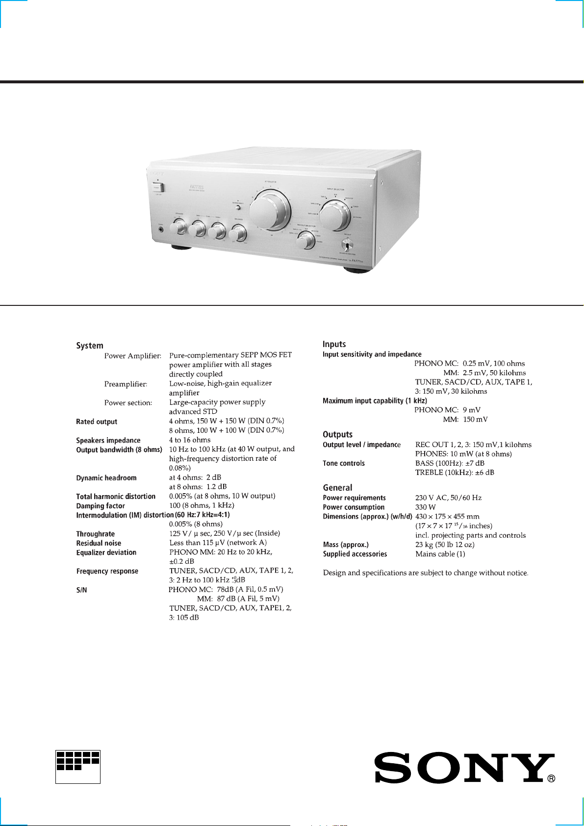
TA-FA777ES
SERVICE MANUAL
SPECIFICATIONS
AEP Model
MICROFILM
INTEGRATED STEREO AMPLIFIER

TABLE OF CONTENTS
1. GENERAL
Location of Controls ....................................................... 3
2. DISASSEMBLY ......................................................... 4
3. ELECTRICAL ADJUSTMENT............................ 6
4. DIAGRAMS
4-1. Notes for Printed Wiring Boards
and Schematic Diagrams ................................................ 7
4-2. Printed Wiring Boards
– INPUT/MAIN-B(L)/MAIN-B(R) Boards – ................ 8
4-3. Schematic Diagram
– INPUT(1/2)/MAIN-B(L)/MAIN-B(R) Boards – ........ 9
4-4. Printed Wiring Boards – BALANCE/FUNCTION SW/
SP TM/HP/TONE CONTROL/PRO.LED Boards – ...... 10
4-5. Schematic Diagram – BALANCE/FUNCTION SW/
SP TM/INPUT(2/2)/HP/TONE CONTROL(2/2)/
PRO.LED Boards – ......................................................... 11
4-6. Printed Wiring Boards – MAIN-A/RV/REC OUT/
PS PRE/PS/OUTLET Boards – ...................................... 12
4-7. Schematic Diagram – MAIN-A/
TONE CONTROL(1/2)/RV/REC OUT/PS PRE/PS/
OUTLET Boards –.......................................................... 13
5. EXPLODED VIEWS ................................................ 14
6. ELECTRICAL PARTS LIST ............................... 17
SAFETY-RELATED COMPONENT WARNING!!
COMPONENTS IDENTIFIED BY MARK 0 OR DOTTED
LINE WITH MARK 0 ON THE SCHEMATIC DIAGRAMS
AND IN THE PARTS LIST ARE CRITICAL TO SAFE
OPERATION. REPLACE THESE COMPONENTS WITH
SONY PARTS WHOSE PART NUMBERS APPEAR AS
SHOWN IN THIS MANUAL OR IN SUPPLEMENTS PUBLISHED BY SONY.
2
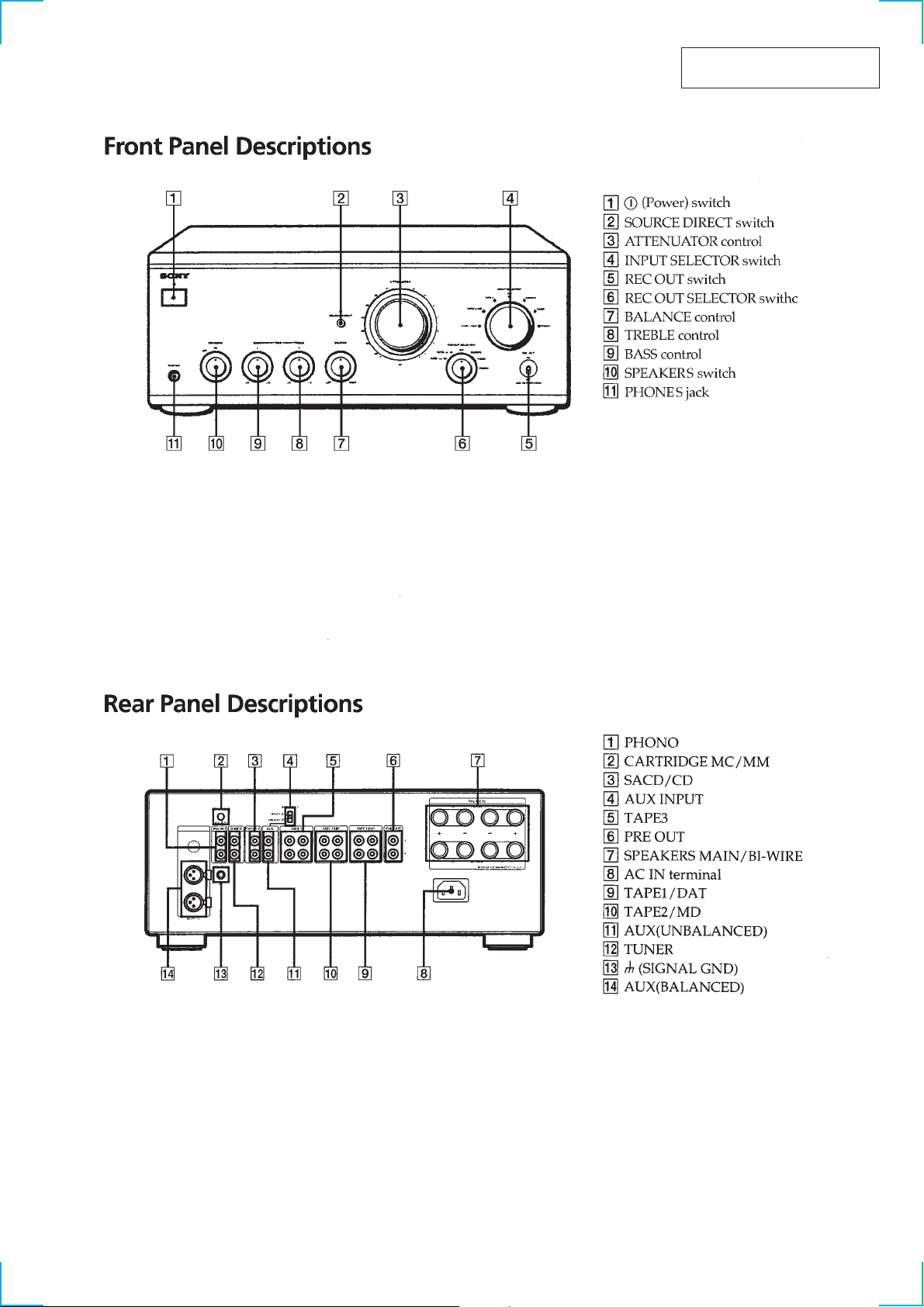
LOCATION OF CONTROLS
SECTION 1
GENERAL
This section is extracted from
instruction manual.
3
SECTION 2
s
DISASSEMBLY
Note: Follow the disassembly procedure in the numerical order given.
FRONT PANEL, TOP board, BOTTOM board
1
four screws
(FLAT HEAD)
2
top board
7
two screws
(BV 3
×
8)
9
front panel
qa
two foots
1
four screws
(FLAT HEAD)
qd
bottom board
6
knob (DIA.68)
3
screw
5
screw
4
knob (DIA.48)
SUB CHASSIS, FUN-SW BOARD
9
switch, push
(AC power)
5
sub chassis
6
3
connector
4
screw
(BV 3 × 8)
7
power botton
assy
(CN806)
8
qh
connector
(CN304)
two connectors
(CN807, 808)
0
two screws
(B 4
three screws
×
8)
(BV 3
×
20)
qs
three screws
(BV 3
1
four screws
(BV 3 × 8)
qs
five screw
(BV 3 × 8)
qa
three foots
0
×
8)
1
three screws
(B 4
two screws
(BV 3 × 8)
2
shield plate
×
20)
8
two screws
( 3 × 6)
4
four screws
(BV 3 × 8)
0
knob (DIA.29)
qa
light interception sheet (B)
qs
nut
qf
nut
4
two screws
(BV 3 × 8)
qg
FUN-SW board
4
four screws
(BV 3 × 8)
qd
rotary switch
(remote type)
4
HEAT SINK (L) / (R) ASSY
)
3
4
three connectors
(CN501, 502, 503)
1
two screws
(4 × 8)
heat sink (L) assy
2
two screws
(4 × 8)
2
two screws
(4 × 8)
1
two screws
(4 × 8)
5
heat sink (R) assy
6
three connectors
(CN551, 552, 553
MAIN A board, PS-PRE board
5
four connectors
(CN802, 803, 804, 805)
3
two screws
(BV 3
9
Chassis (I)
6
×
8)
PS-PRE board
three connectors
(CN51, 52, 53)
7
four connectors
(CN401, 402, 403, 404)
MAIN A board
8
three connectors
(CN203, 204, 205)
4
rod
2
three screws
(BV 3
1
×
8)
two screws
×
8)
(3
5
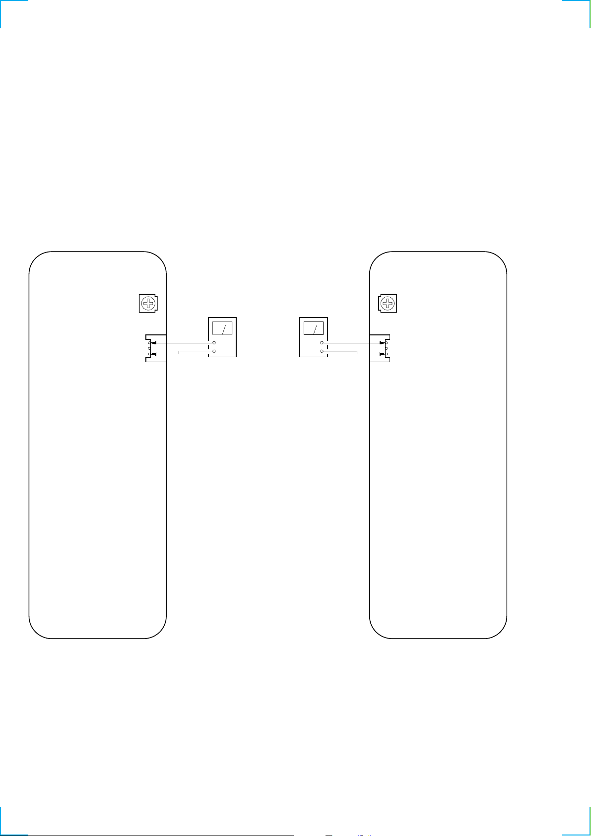
SECTION 3
ELECTRICAL ADJUSTMENT
Note: Adjustment should be performed 5 minutes later, after the power
switch is on.
Bias Adjustment
Setting:
ATTENUATOR (Volume) control: minimum
Input signal: No signal input
Procedure:
Adjust RT501 (L-CH) and RT551 (R-CH) for 70 mV reading on
the VTVM.
Adjustment Location:
– MAIN-B (L) Board (Component side) – – MAIN-B (R) Board (Component side) –
RT501
CN504
1
3
level meter
(0.3V DC range)
+
–
L-CH
level meter
(0.3V DC range)
+
–
R-CH
RT551
CN554
3
1
6
SECTION 4
PRO. LED board
HP board
TONE CONTROL board
MAIN-B (L) board
RV board
FUNCTION SW board
MAIN-A board
REC OUT board
PS board
MAIN-B (R) board
BALANCE board
INPUT board
SP TM board
OUTLET board
PS-PRE board
DIAGRAMS
4-1. NOTE FOR PRINTED WIRING BOARDS AND SCHEMATIC DIAGRAMS
(In addition to this, the necessary note is printed in each block.)
Note on Schematic Diagram:
• All capacitors are in µF unless otherwise noted. pF: µµF
50 WV or less are not indicated except for electrolytics
and tantalums.
• All resistors are in Ω and 1/
specified.
• 2 : nonflammable resistor.
• 5 : fusible resistor.
• C : panel designation.
NOTE: The components identified by mark 0 or dotted line
with mark 0 are critical for safety.
Replace only with part number specified.
• U : B+ Line.
• V : B– Line.
• H : adjustment for repair.
• Voltages and waveforms are dc with respect to ground
under no-signal conditions.
no mark: POWER ON
• Voltages are taken with a V OM (Input impedance 10 MΩ).
Voltage variations may be noted due to normal production tolerances.
• Signal path.
I : PHONO
W or less unless otherwise
4
Note on Printed Wiring Boards:
• X : parts extracted from the component side.
• b : Pattern from the side which enables seeing.
• Indication of transistor.
Q
B
CE
These are omitted.
Q
B
CE
These are omitted.
• Circuit Boards Location
77
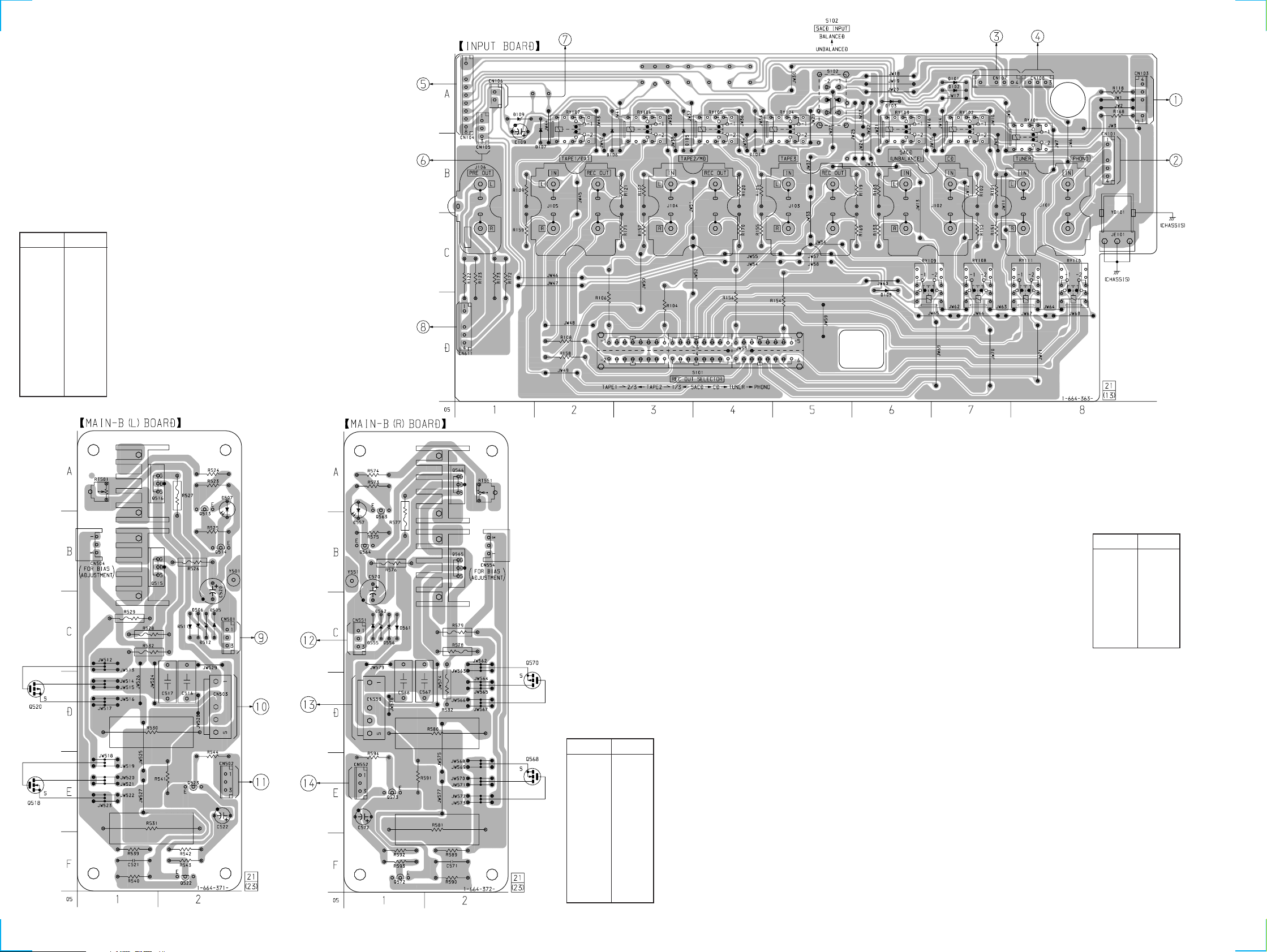
TA-FA777ES
4-2. PRINTED WIRING BOARDS – INPUT/MAIN-B (L) /MAIN-B (R) Boards –
• See page 7 for Circuit Boards Location.
(Page 10)
(Page 10)
• Semiconductor
Location
– MAIN-B (L) Board –
Ref. No. Location
D505 C-2
D506 C-2
D507 A-2
D511 C-2
D512 C-2
Q513 A-2
Q514 B-2
Q515 B-1
Q516 A-1
Q518 E-1
Q520 D-1
Q522 F-2
Q523 E-2
(Page 10)
(Page 10)
(Page 10) (Page 12)
(Page
12)
(Page
12)
(Page 12)
(Page 12)
(Page 10)
(Page 12)
(Page 12)
(Page 10)
• Semiconductor
Location
– INPUT Board –
Ref. No. Location
D101 A-7
D102 A-7
D103 A-6
D104 A-4
D105 A-3
D106 A-2
D107 A-2
D108 C-6
D109 A-1
• Semiconductor
Location
– MAIN-B (R) Board –
Ref. No. Location
D555 C-1
D556 C-1
D557 A-1
D561 C-1
D562 C-1
Q563 A-1
Q564 B-1
Q565 B-2
Q566 A-2
Q568 E-2
Q570 D-2
Q572 F-1
Q573 E-1
88
 Loading...