

Sony STSV-7 Service manual
ST-SV7
SERVICE MANUAL
Ver 1.0 2001.06
ST-SV7 is the tuner section
in MHC-SV7AV.
SPECIFICATIONS
Tuner section
FM stereo, FM/AM superheterodyne tuner
FM tuner section
Tuning range 87.5 – 108.0 MHz
Antenna FM lead antenna
Antenna terminals 75 ohm unbalanced
Intermediate frequency 10.7 MHz
E Model
AM tuner section
Tuning range
Middle Eastern model:
Other models:
Antenna AM loop antenna
Antenna terminals External antenna terminal
Intermediate frequency 450 kHz
Dimensions (w/h/d)
Mass
Design and specifications are subject to change
without notice.
531 – 1,602 kHz
(with the interval set at 9 kHz)
531 – 1,602 kHz
(with the interval set at 9 kHz)
530 – 1,710 kHz
(with the interval set at 10 kHz)
Approx. 280 x 108 x 340 mm
Approx. 2.1 kg
FM STEREO, FM/AM
9-873-152-01 Sony Corporation
2001F0500-1 Home Audio Company
C 2001.6 Shinagawa Tec Service Manual Production Group
SUPERHETERODYNE TUNER
ST-SV7
SECTION 1
SERVICING NOTES
TABLE OF CONTENTS
1. SERVICING NOTES ................................................ 2
2. GENERAL
Location of Controls ....................................................... 3
Setting the Time .............................................................. 4
3. DISASSEMBLY
3-1. Disassembly Flow ........................................................... 5
3-2. Cover ............................................................................... 6
3-3. Front Panel Section ......................................................... 6
3-4. PANEL Board, SIRCS Board ......................................... 7
3-5. Tuner pack (FM/AM)...................................................... 7
3-6. MAIN Board ................................................................... 8
3-7. DSP Board....................................................................... 8
4. TEST MODE.............................................................. 9
5. DIAGRAMS
5-1. Note for Printed Wiring Boards and
Schematic Diagrams ....................................................... 10
5-2. Schematic Diagram – MAIN Board (1/2) – .................. 12
5-3. Schematic Diagram – MAIN Board (2/2) – .................. 13
5-4. Printed Wiring Board – MAIN Board – ........................ 14
5-5. Printed Wiring Board – DSP Board –............................ 15
5-6. Schematic Diagram – DSP Board (1/2) – ..................... 16
5-7. Schematic Diagram – DSP Board (2/2) – ..................... 17
5-8. Printed Wiring Boards – PANEL Section – .................. 18
5-9. Schematic Diagram – PANEL Section –....................... 19
5-10. IC Pin Function Description ........................................... 20
6. EXPLODED VIEWS
6-1. Cover, Front Panel Section ............................................. 26
6-2. Chassis Section ............................................................... 27
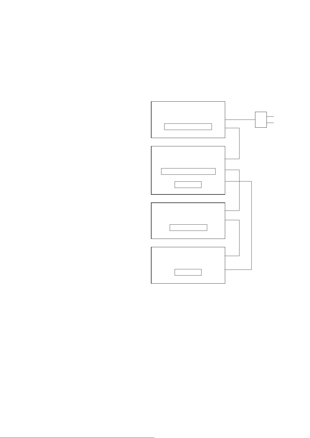
This set is a component of the MHC-SV7AV.
The MHC-SV7AV system configuration is as shown below, and
therefore it does not operate normally unless all four components
are connected.
In performing the repair, connect all components with the system
cables.
Note: The precaution to the users is described on the label stuck
on the back panel (video CD player) and in the troubleshooting
section in the Operation Manual.
System Configuration:
AC IN
TA
POWER SUPPLY
ST
MASTER & GRAPHIC µcon
DISPLAY
MCE
HTC & VMP µcon
7. ELECTRICAL PARTS LIST ............................... 28
Notes on chip component replacement
• Never reuse a disconnected chip component.
• Notice that the minus side of a tantalum capacitor may be dam-
aged by heat.
SAFETY-RELATED COMPONENT WARNING!!
COMPONENTS IDENTIFIED BY MARK 0 OR DOTTED
LINE WITH MARK 0 ON THE SCHEMATIC DIAGRAMS
AND IN THE PARTS LIST ARE CRITICAL TO SAFE
OPERATION. REPLACE THESE COMPONENTS WITH
SONY PARTS WHOSE PART NUMBERS APPEAR AS
SHOWN IN THIS MANUAL OR IN SUPPLEMENTS PUBLISHED BY SONY.
TC
TC µcon
2
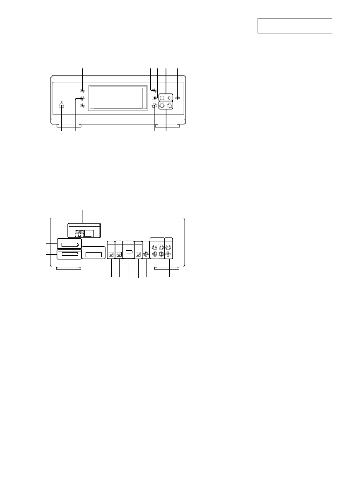
LOCATION OF CONTROLS
– Front Panel –
SECTION 2
GENERAL
ST-SV7
This section is extracted from
instruction manual.
– Rear Panel –
2
3
qk qlw; wa ws
—
+
+
—
wdwfwgwhwj
1
4 5 6 7
8
09qa
CLOCK/TIMER wh (13, 25, 34)
DISPLAY qk (13, 18, 33, 40)
ENTER ws (22)
IR receptor wj
PRESET –/+ wd (22)
STEREO/MONO ql (22)
TIMER SELECT wg (26, 35)
TUNER/BAND wf (22)
TUNER MEMORY w; (22)
TUNING –/+ wa (22)
1 ANTENNA terminal
2 SYSTEM CONTROL 1 connector (TO TA-SV7AV)
3 SYSTEM CONTROL 2 connector (TO TA-SV7AV)
4 SYSTEM CONTROL 3 connector
(FROM MCE-SV7)
5 OPTICAL IN terminal
6 OPTICAL IN terminal (FROM MCE-SV7)
7 SYSTEM CONTROL 4 connector (TO TC-S3)
8 OPTICAL OUT terminal
9 SUB WOOFER OUT jack
0 MD IN/OUT jack
qa VIDEO (AUDIO) IN jack
3
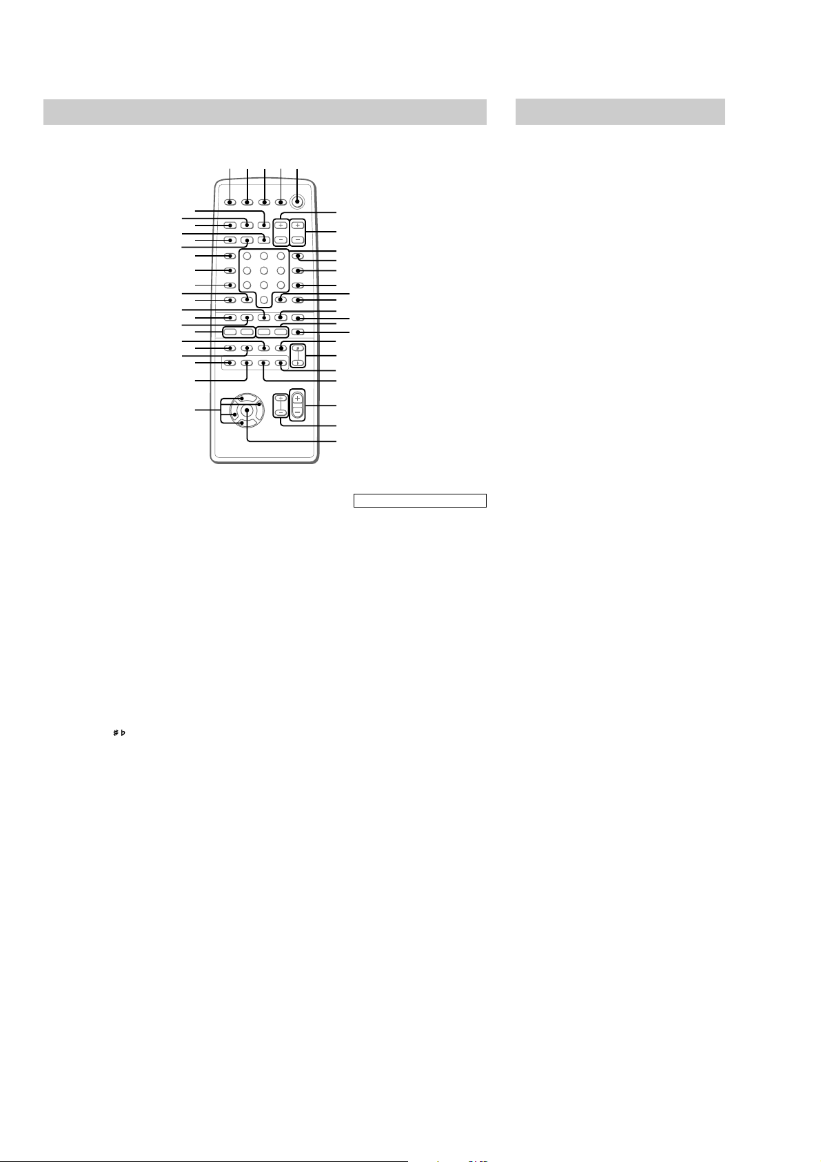
ST-SV7
Remote Control
CHECK qd (17)
CLEAR qs (17, 19)
CLOCK/TIMER SELECT 3
(26, 35)
CLOCK/TIMER SET 2 (13, 25,
34)
DBFB ej (27)
DIGITAL r; (36, 40)
DISPLAY rd (13, 18, 33, 40)
D.SKIP 9 (14, 16, 20, 21)
ENTER wf (11, 13, 15, 17, 21,
22, 25, 26, 30–33, 35)
EQ wh (31)
EQ ON/OFF wa (32)
FILE SELECT +/– wd (27, 28,
32)
FUNCTION el (10, 14–17, 24,
25, 34, 36)
GROOVE ek (27)
KARAOKE PON qk (33)
KEY CONTROL
MD rs (36)
Numeric buttons 8 (15, 16, 19,
20, 21)
ON SCREEN wk (18)
/ ql (33)
1234 5
rg
rf
rd
rs
ra
r;
el
ek
ej
eh
ef
es
e;
wk
eg
ed
ea
wl
wj
O
wh
V
wg
Bb
v
PICTURE EFFECT wl (21)
PRESET –/+, PREV/NEXT ea
(14, 15, 20, 22)
REPEAT q; (15, 16)
RETURN O eg (15)
PLAY MODE qa (14, 16, 17, 25)
SELECT CD N es (14–17, 19,
21)
SET UP w; (11, 13, 30, 32, 33)
SLEEP 1 (34)
SPECIAL MENU e; (19, 20, 21)
SPECTRUM ANALYZER rf
(33)
SUR wj (30)
TAPE A nN ef (23)
TAPE B nN qf (23, 24)
TUNER/BAND ed (22)
TUNING –/+ qh (22)
TV CH +/– 7 (10)
TV VOL +/– 6 (10)
TV @/1 4 (10)
TV/VIDEO rg (10)
VIDEO ra (36)
VOL +/– ws
Setting the time
1
Turn on the system.
2
Press CLOCK/TIMER (or CLOCK/TIMER
SET on the remote).
When you set the time for the first time,
6
7
8
9
q;
qa
qs
qd
qf
x
nNnN
Mm>.
X
qh
qk
qg
qj
ql
w;
wa
ws
wd
wf
BUTTON DESCRIPTIONS
@/1 (power) 5
X (pause) qj
x (stop) qg
./> (go back/go forward)
ea
m/M (rewind/fast forward)
qh
O/o/P/p wg
>10 eh
proceed to step 5.
3
Press O or o repeatedly to select
“CLOCK SET”.
4
Press ENTER (A/V amplifier or remote).
5
Press O or o repeatedly to set the hour.
6
Press ENTER (A/V amplifier or remote).
7
Press O or o repeatedly to set the
minutes.
8
Press ENTER (A/V amplifier or remote).
Tip
If you have made a mistake or want to change the
time, start over from step 2.
Note
The clock settings are canceled when you disconnect
the power cord or if a power failure occurs.
4
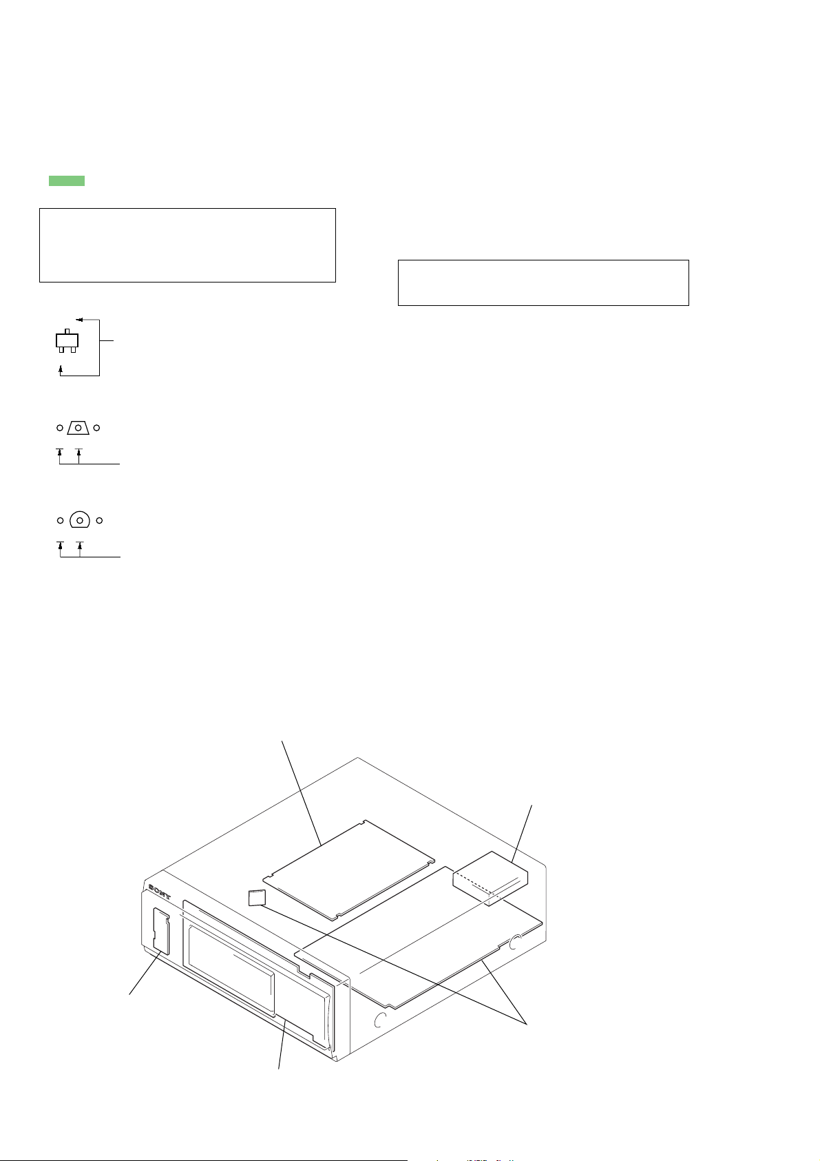
• This set can be disassembled in the order shown below.
3-1. DISASSEMBLY FLOW
SET
3-2. COVER
(Page 6)
ST-SV7
SECTION 3
DISASSEMBLY
3-3. FRONT PANEL SECTION
(Page 6)
3-4. PANEL BOARD,
SIRCS BOARD
(Page 7)
3-5. TUNER PACK (FM/AM)
(Page 7)
3-6. MAIN BOARD
(Page 8)
3-7. DSP BOARD
(Page 8)
5
ST-SV7
)
Note: Follow the disassembly procedure in the numerical order given.
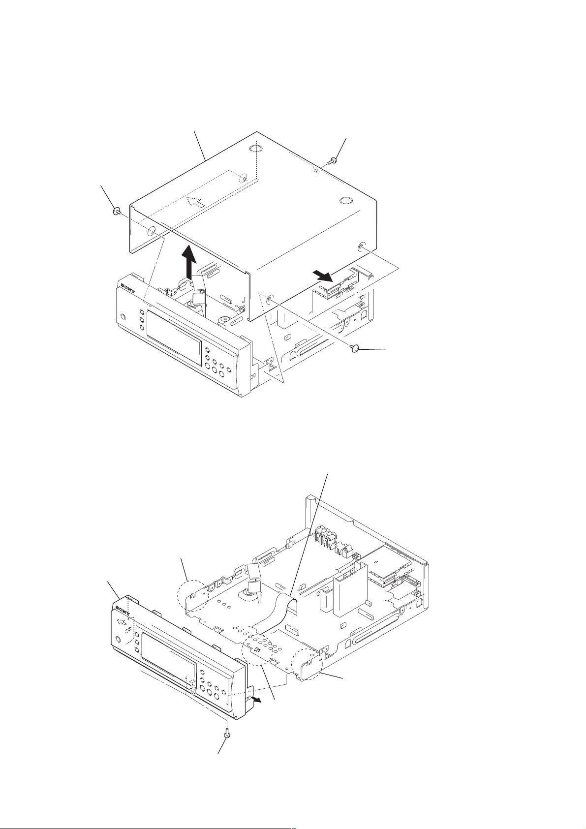
3-2. COVER
3
cover
2
two screws
(case 3 TP2)
1
screw
(+BVTT3
×
6 (S))
3-3. FRONT PANEL SECTION
3
two claws
4
front panel section
2
1
wire (flat type) (19 core)
(CN502)
two screws
(case 3 TP2
3
two claws
3
claw
2
three screws
(BVTP3
×
8)
6
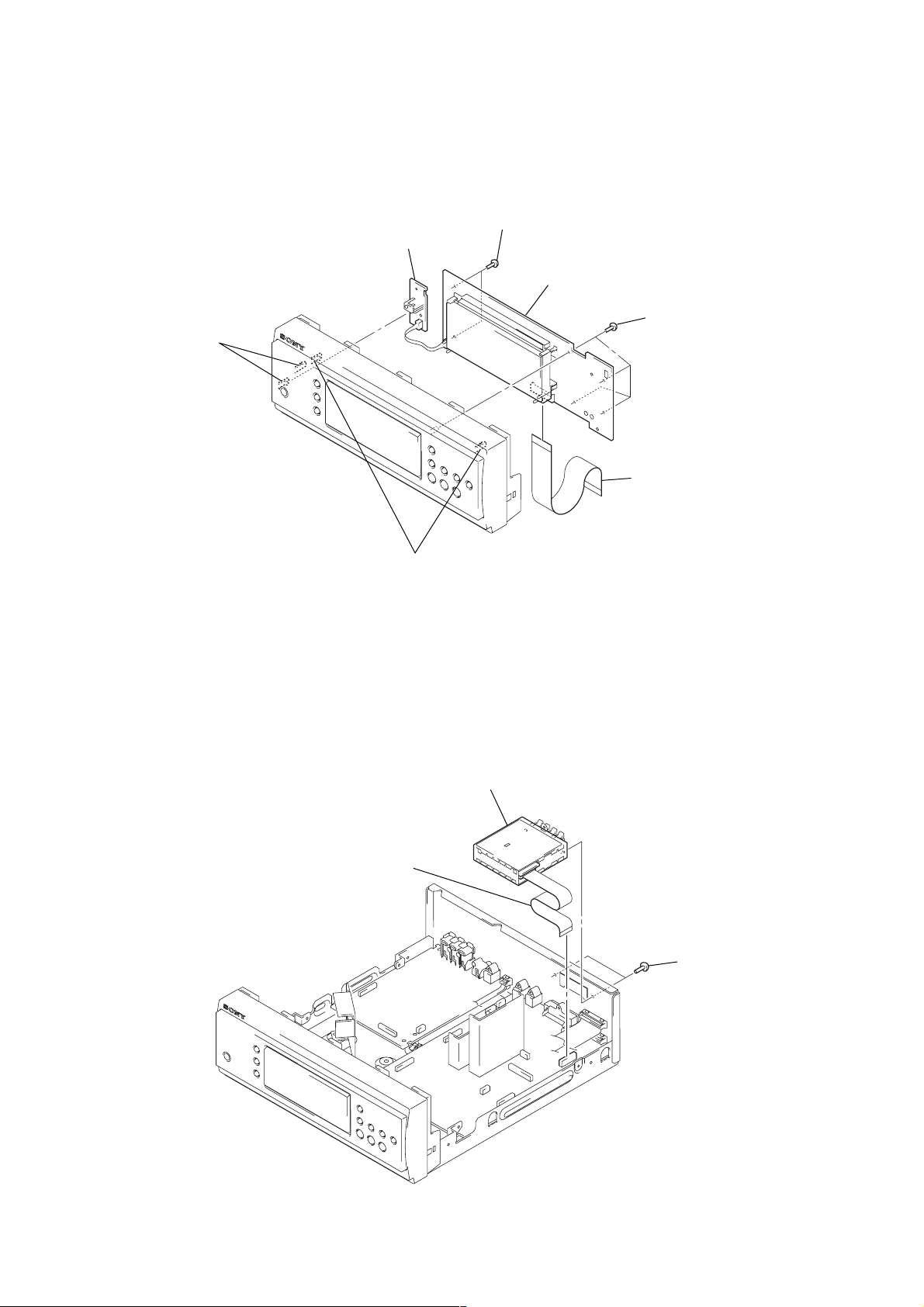
3-4. PANEL BOARD, SIRCS BOARD
)
6
SIRCS board
5
two claws
2
two screws
(BVTP2.6
×
8)
4
PANEL board
2
four screws
(BVTP2.6
1
wire (flat type) (19 core
(CN602)
×
8)
ST-SV7
3-5. TUNER PACK (FM/AM)
1
wire (flat type) (11 core)
(CN506)
3
two claws
3
tuner pack (FM/AM)
2
two screws
(BVTP3 × 8)
7
ST-SV7
r
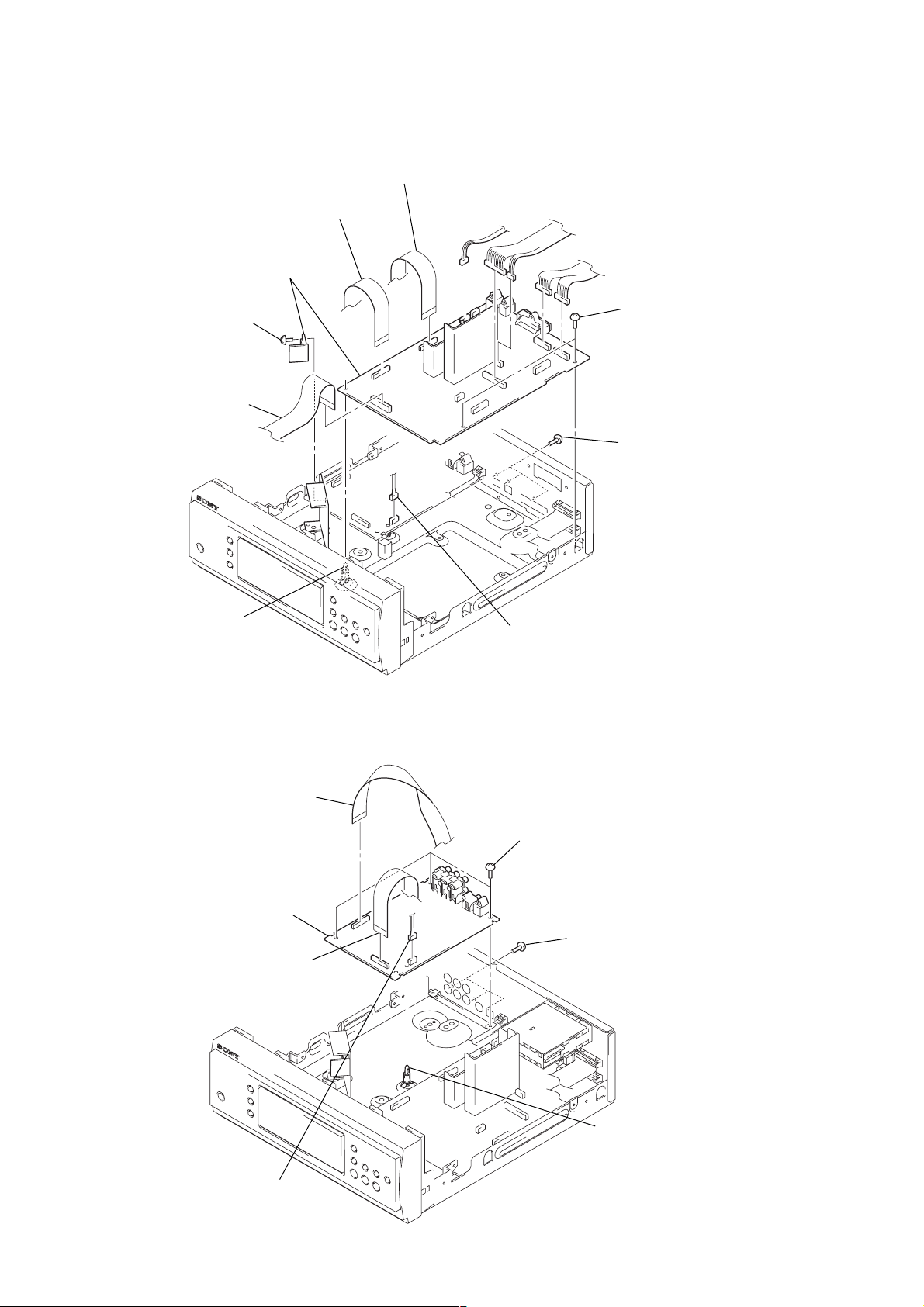
3-6. MAIN BOARD
4
1
wire (flat type) (19 core)
(CN502)
screw
(BVTP3
1
wire (flat type) (21 core)
(CN509)
6
MAIN board
×
8)
1
wire (flat type) (23 core)
(CN508)
2
five connectors
(CN510, 5031, 5032, 5041, 5042)
4
two screws
(BVTP3 × 8)
3
three screws
(BVTP3 × 8)
5
PC board holder
3-7. DSP BOARD
1
1
wire (flat type) (23 core)
(CN603)
6
DSP board
wire (flat type) (21 core)
(CN602)
2
connector
(CN601)
4
three screws
(BVTP3 × 8)
3
three screws
(BVTP3
×
8)
5
PC board holde
2
connector
(CN601)
8

SECTION 4
TEST MODE
ST-SV7
Note: Use following buttons in the test mode.
no mark: Button of tuner unit (ST-SV7)
1
*
: Button of amplifier unit (TA-SV7AV)
2
*
: Button of CD unit (MCE-SV7)
[MC Cold Reset]
• The cold reset clears all data including preset data stored in the
RAM to initial conditions. Execute this mode when returning
the set to the customer.
Procedure 1:
1. Press the ?/1 *1 button to turn the power ON.
2. While pressing the [DIGITAL]*1 button, press the
[DISPLAY] button.
3. The set is reset, and becomes standby state.
Procedure 2:
1. Press the ?/1 *1 button to turn the power ON.
2. While pressing the both [PLAY MODE]*2 and x *2 buttons,
press the M *2 button.
3. The set is reset, and becomes standby state.
[MC Hot Reset]
• This mode resets the set with the preset data kept stored in the
memory. The hot reset mode functions same as if the power
cord is plugged in and out.
Procedure 1:
1. Press the ?/1 *1 button to turn the power ON.
2. While pressing the both [STEREO/MONO] and [CINEMA
STUDIO C]*
3. The set is reset, and becomes standby state.
Procedure 2:
1. Press the ?/1 *1 button to turn the power ON.
2. While pressing the both [PLAY MODE]*2 and x *2 buttons,
press the m *2 button.
3. The set is reset, and becomes standby state.
[Change-over the AM Tuning Interval]
(EXCEPT Sauidi Arabia model)
• The AM tuning interval can be changed over 9 kHz or 10 kHz.
Procedure:
1. Press the ?/1 *1 button to turn the power ON.
2. Turn the [FUNCTION] *
the [TUNER/BAND] button to select the BAND “AM”.
3. Press the ?/1 *1 button to turn the power OFF.
4. While pressing the [ENTER] button, press the ?/1 *1 button,
and the display on the fluorescent indicator tube changes to
“AM 9 K STEP” or “AM 10 K STEP”, and thus the tuning
interval is changed over.
1
buttons, press the [TIMER SELECT] button.
1
knob to select “TUNER”, and press
[GC Test Mode]
Enter the GC Test Mode mode
Procedure 1:
1. Press the ?/1 *1 button to turn the power ON.
2. While pressing the both [STEREO/MONO] and [CINEMA
STUDIO C]*
1
buttons, press the [CLOCK/TIMER] button.
3. LEDs and fluorescent indicator tube are all turned on of all
units.
Procedure 2:
1. Press the ?/1 *1 button to turn the power ON.
2. While pressing the both [PLAY MODE]*2 and x *2 buttons,
press the Z (DISC 1)*2 button.
3. LEDs and fluorescent indicator tube are all turned on of all
units.
Version Display Mode
Procedure:
1. Enter the GC test mode.
2. Each time the [TUNER MEMORY] or [DISC 1]*2 button is
pressed, microcomputer or mechanism deck version is
displayed of each unit.
3. Press the [TUNING +] or [DISC 3]*2 button to detail is displayed
the version.
Key Check Mode
Procedure:
1. Enter the GC test mode.
2. Press the [TUNING -- ] or [DISC 2]*2 button to set the key check
mode.
3. In the key check the mode, the fluorescent indicator tube
displays “K 0 J 0 V 0” . Each time a button is pressed, “K”
value increases. However, once a button is pressed, it is no
longer taken into account.
VACS Level Display Mode
Procedure:
1. Enter the GC test mode.
2. Press the
[TUNING +] or [DISC 3]*
2
button to display VACS
level on the fluorescent indicator tube.
Segment Check Mode
Procedure:
1. Enter the GC test mode.
2. Press the [ENTER] or x *2 button to set the segment check
mode.
3. In the segment check the mode. Each [ENTER] or x *
button is pressed, the fluorescent indicator tube displays is
switching variously.
2
[Change-over of VACS ON/OFF]
1. Press the ?/1 *1 button to turn the power ON.
2. While pressing the both [STEREO/MONO] and [CINEMA
STUDIO C]*
1
buttons, press the [CINEMA STUDIO B] button,
and VACS ON/OFF is change over.
Releasing the GC Test Mode
• To release from this mode, press three b uttons in the same manner
as entering this mode or disconnect the power cord.
9
ST-SV7
SECTION 5
DIAGRAMS
5-1. NOTE FOR PRINTED WIRING BOARDS AND SCHEMATIC DIAGRAMS
Note on Printed Wiring Board:
• X : parts extracted from the component side.
• Y : parts extracted from the conductor side.
• : Pattern from the side which enables seeing.
(The other layers' patterns are not indicated.)
Caution:
Pattern face side: Parts on the pattern face side seen from
(Conductor Side) the pattern face are indicated.
Parts face side: Parts on the parts face side seen from
(Component Side) the parts face are indicated.
• Indication of transistor.
C
Q
B
B
B
E
Q
CE
These are omitted.
These are omitted.
Q
CE
These are omitted.
Note on Schematic Diagram:
• All capacitors are in µF unless otherwise noted. pF: µµF
50 WV or less are not indicated except for electrolytics
and tantalums.
• All resistors are in Ω and 1/
specified.
f
•
• 5 : fusible resistor.
• C : panel designation.
Note: The components identified by mark 0 or dotted line
• A : B+ Line.
• B : B– Line.
• Voltages and waveforms are dc with respect to ground
• V oltages are taken with a VOM (Input impedance 10 MΩ).
• Waveforms are taken with a oscilloscope.
• Signal path.
• Abbreviation
: internal component.
with mark 0 are critical for safety.
Replace only with part number specified.
under no-signal (detuned) conditions.
no mark : TUNER (FM/AM)
( ) : CD PLAY
〈〈 〉〉 : AC OFF
Voltage variations may be noted due to normal production tolerances.
Voltage variations may be noted due to normal production tolerances.
F : TUNER (FM/AM)
E : T APE PLA Y
G : RECORD
J : CD PLAY
c : DIGITAL INPUT
N : MIC INPUT
EA : Saudi Arabia model
SP : Singapore model
TH : Thailand model
: Impossible to measure
∗
4
W or less unless otherwise
• Circuit Boards Location
SIRCS board
DSP board
TUNER PACK
MAIN board
PANEL board
10
ST-SV7
• Waveforms
– MAIN Board –
1 IC501 qa (XCOUT)
30.5 µs
2 IC501 qd (XOUT)
2.6 Vp-p
2.7 Vp-p
– DSP Board –
1 IC601 9 (MCLK1), IC604 w; (XMCK),
wa (XOUT)
4 Vp-p
74.1 ns
2 IC601 qf (SCKOUT)
4.6 Vp-p
5 IC601 ws (KFSIO), IC604 qd (CKOUT)
4.4 Vp-p
88.6 ns
6 IC601 wk (LRCKI2), IC604 qg (LRCK)
3.9 Vp-p
• IC Block Diagrams
– DSP Board –
IC604 LC89056W-E
36
CE
37
38
CL
39XSEL
MODE0
MODE1
DOSEL0
DOSEL1
CKSEL0
CKSEL1
XMODE
MICROCOMPUTER
40
41
42DGND
43DVDD
44
45
46
47
48
INTERFACE
DI
DO
35
BPSYNC
ERROR
3334
DGND
ERR9P
31
SAMPLING
FREQUENCY
LOCK
DETECT
DATA
DEMODULATOR
INPUT
CIRCUIT
XSEL
VF
30
DETECT
F2
C BIT
F1
X’ TAL
TIMING
F0
252627282932
PLL
CSFLAG
PA/PB
DETECT
AUDIO
24
23
EMPHA
22
XIN
21
XOUT
20
XMCK
19 DVDD
18 DGND
17
XSTATE
16
DATAO
LRCK
15
BCK
14
CKOUT
13
62.5 ns
– PANEL Board –
1 IC601 id (XOUT)
250 ns
3.5 Vp-p
74.1 ns
3 IC601 ql (LRCKO), IC605 5 (LRCK),
IC606 3 (LRCK (I))
3.8 Vp-p
22.7 µs
4 IC601 w; (BCKO), IC605 4 (BCK),
IC606 1 (BCK (I))
3.6 Vp-p
354 ns
22.7 µs
7 IC601 wl (BCKI2), IC604 qf (BCK)
354 ns
8 IC606 qh (MCLK (I))
3.7 Vp-p
74.1 ns
4 Vp-p
IC605 AK4527
LOOP1
LOOP0/SDA/CDTI
44 43 42 41 40 39 38 37 36 35 34
1
SDOS
I2C
2
SMUTE
3
BICK
4
LRCK
5
SDTI1
6
SDTI2
7
SDTI3
8
SDTO
9
10
11
FORMAT
CONVERTER
12 13 14 15 16 17 18 19 20 21 22
DEM1
DAUX
DFS
1 2 3 4
DOUT
DISEL
DIF1/SCL/CCLK
DIF0/CSN
P/SN
MCLK
DZF1
AUDIO
INTERFACE
PDN
TVDD
DVSS
DVDD
DEM0
DINO
AVSS
ICKS2
AVDD
ICKS1
VREFH
CIRCUIT
OUTPUT
CIRCUIT
ICKS0
DINI
VCOM
INPUT
CAD1
CAD0
5
DIN2
33
32
31
30
29
28
27
26
25
24
23
6
DGND
DZF2
RIN+
RIN–
LIN+
LIN–
ROUT1
LOUT1
ROUT2
LOUT2
ROUT3
LOUT3
7
DVDD
8 9 10
R
VIN
LPF
11
12
AVDD
AGND
1111
 Loading...