Page 1
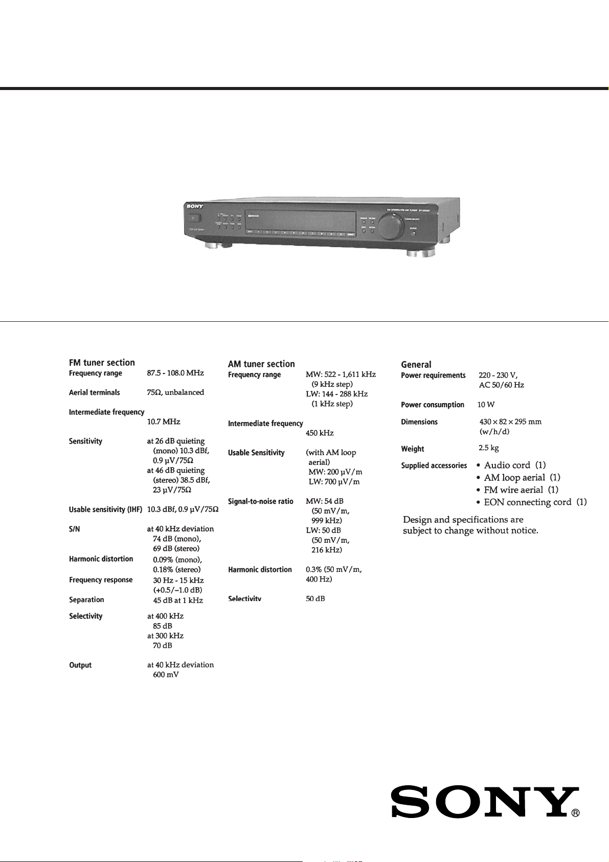
ST-SE520
SERVICE MANUAL
SPECIFICATIONS
AEP Model
UK Model
FM STEREO FM-AM TUNER
1
Page 2
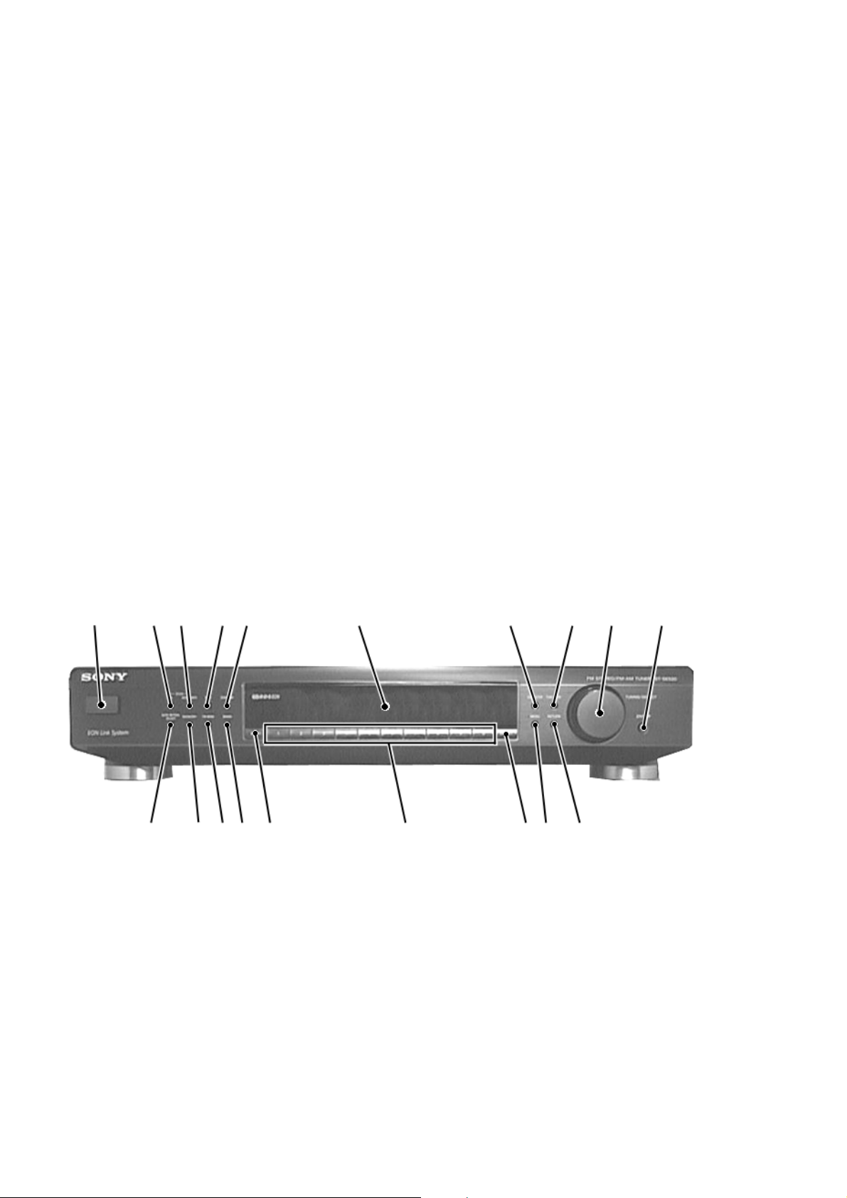
TABLE OF CONTENTS
SAFETY-RELATED COMPONENT WARNING !!
1. GENERAL .......................................................................... 2
2. TEST MODE .......................................................................3
3. ELECTRICAL ADJUSTMENTS ................................. 5
4. DIAGRAMS
4-1. Circuit Boards Location ........................................................ 5
4-2. Schematic Diagram – Tuner Section – ................................. 6
4-3. Printed Wiring Board – Tuner Section – ............................... 7
4-4. Schematic Diagram – Display Section – .............................. 8
4-5. Printed Wiring Board – Display Section –............................9
4-6. IC Pin Function ................................................................... 10
4-7. IC Block Diagrams.............................................................. 11
5. EXPLODED VIEW ......................................................... 12
6. ELECTRICAL PARTS LIST ........................................ 13
SECTION 1
GENERAL
COMPONENTS IDENTIFIED BY MARK 0 OR DOTTED LINE
WITH MARK 0 ON THE SCHEMATIC DIAGRAMS AND IN
THE PARTS LIST ARE CRITICAL TO SAFE OPERATION.
REPLACE THESE COMPONENTS WITH SONY PARTS
WHOSE PART NUMBERS APPEAR AS SHOWN IN THIS
MANUAL OR IN SUPPLEMENTS PUBLISHED BY SONY.
Front Panel Descriptions
11
1 ! (Power)switch
2 EON TA button
3 EON NEWS/INFO button
4 PTY button
5 DISPLAY button
6 Display window
7 CHARACTER button
8 TUNE MODE button
9 TUNING/SELECT knob
10 ENTER button
7
131214 15 16 17 18
11 AUTO-BETICAL SELECT button
12 MEMORY button
13 FM MODE button
14 BAND button
15 SHIFT button
16 Numeric buttons
17 DIRECT button
18 MENU button
19 RETURN button
9
823 4 651 10
19
2
Page 3
SECTION 2
TEST MODE
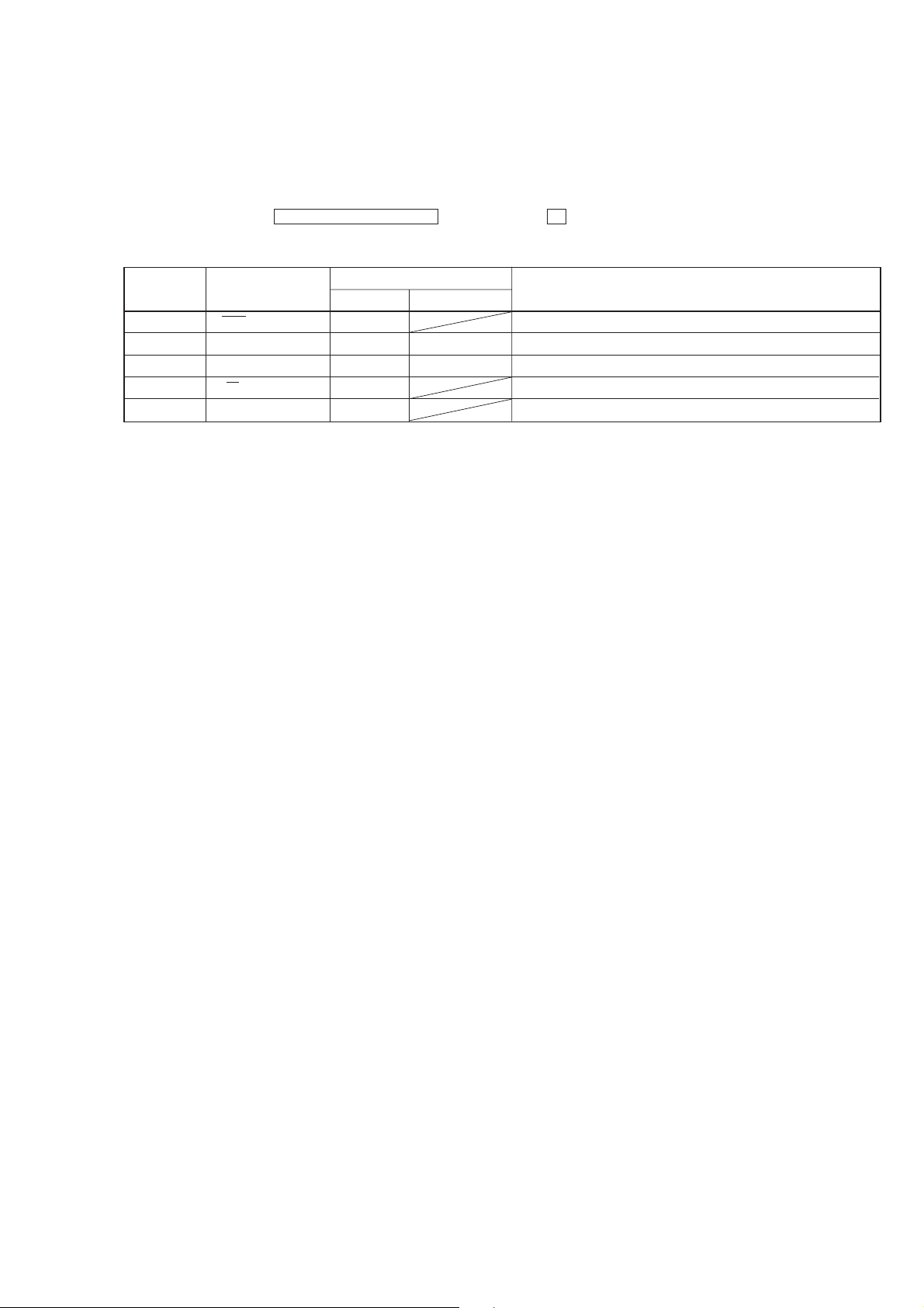
1. Circuit Check Mode
Set to the reception frequency that the circuit can STEREO RDS stations. (Set the input level to above 70 dB.)
This enables circuit check to be performed in any of the reception modes-FM, AM (MW, L W). Set to a desir ed band before setting the test
mode.
1. Turn OFF the power.
2. While pressing 4 and AUTO-BETICAL SELECT together, turn ON ! .
• The items in the following table will be checked automatically in order every 2 seconds.
Display Items
Tuned
IF Frq
Sig Level
Stereo
RDS Signal
AST signal =LOW
IF COUNT OK
SI LEVELh70dB
ST signal=LOW
RDS DATA OK
FM RDS
OK or NG
OK or NG
OK or NG
OK or NG
OK or NG
DISPLAY
AM (MW, LW)
OK or NG
OK or NG
NG
IC201 NG, RV201 adjustments
TB101, IC201 NG
TB101 NG
TB101 NG
IC802 NG
3
Page 4
NOTE : The preset data will be erased when this test mode is used. Therefore, take down the data before setting this mode and preset the
data again after completing operations in this mode.
2. Display Tube Check and KEY Check mode
1. Turn OFF the power.
2. While pressing 1 and AUTO-BETICAL SELECT together, turn ON ! .
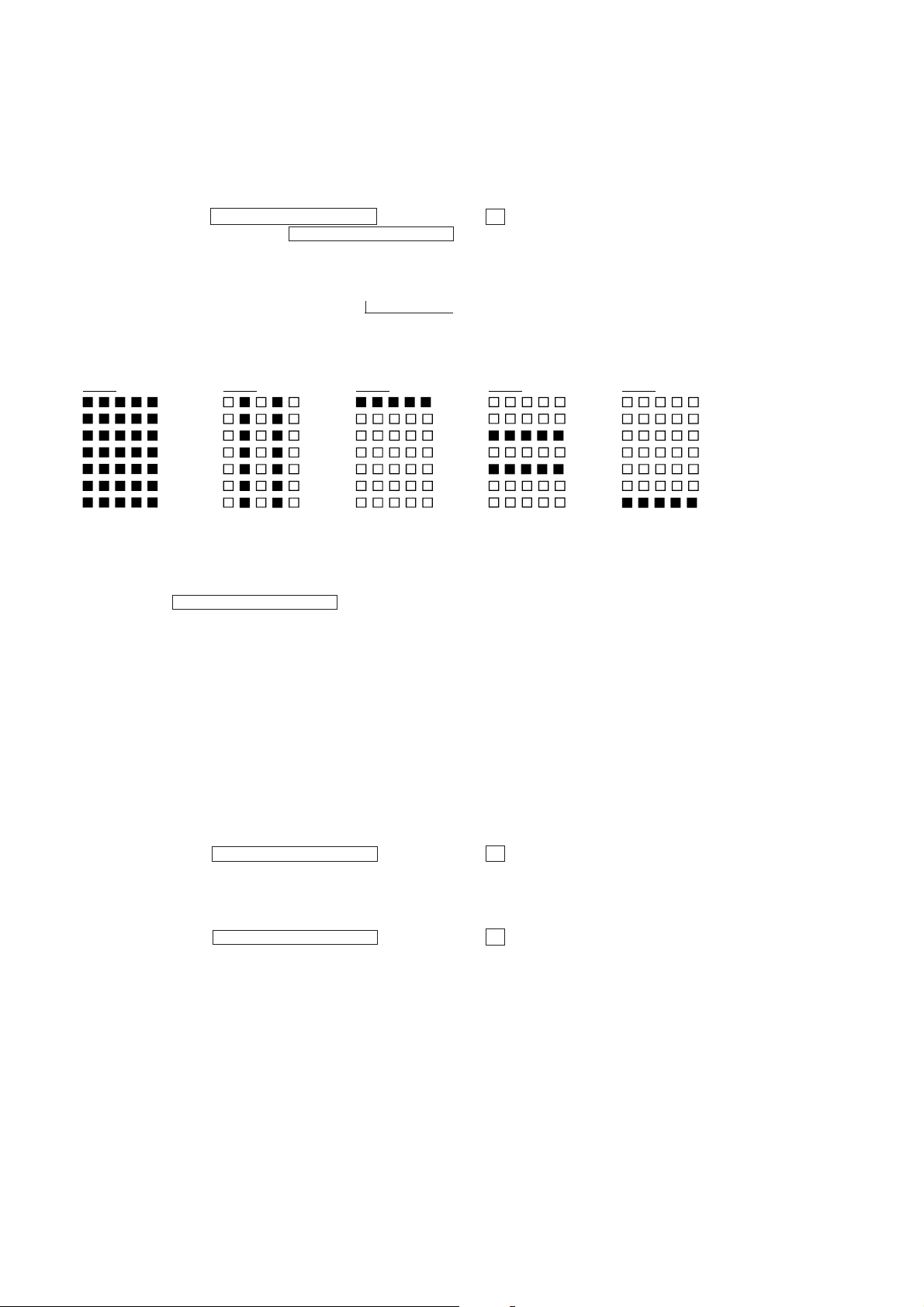
3. While continuously pressing 1 and AUTO-BETICAL SELECT together, check the following.
Microcomputer version indication (1 sec) t All light up “7F” t Dot area only “60” t Dot area only “7E”
Indication test pattern
1 7F
The display changes every 1 sec.
4. Release 1 and AUTO-BETICAL SELECT . The KEY CHECK mode will be set.
5. All key numbers will be displayed.
Key Number : 25
6. Each time the key is pressed, the key number will be counted down.
Each key will be counted only once, at the first time.
2 60 3 7E
T
Dot area only “5F” T Dot area only “3D”
4 3D
5 5F
T
7. When all keys have been pressed, the process will end.
NOTE : As contents of the Factory Preset will be written into memory after completing this check mode, delete contents of memory
according to 4. Forced RESET.
3. Entering the Factory Preset (In case perform just to write memory of the Factory Preset.)
1. Turn OFF the power.
2. While pressing 3 and AUTO-BETICAL SELECT together, turn ON ! .
4. Forced RESET (Used to delete the contents of Factory Preset when it is written into the preset memory.)
Clears all the RAMs and sets the initial state
1. Turn OFF the power.
2. While pressing 5 and AUTO-BETICAL SELECT together, turn ON ! .
3. When “All clear” is indicated on the fluorescent display tube, it means that “Forced Reset” has been completed.
4
Page 5
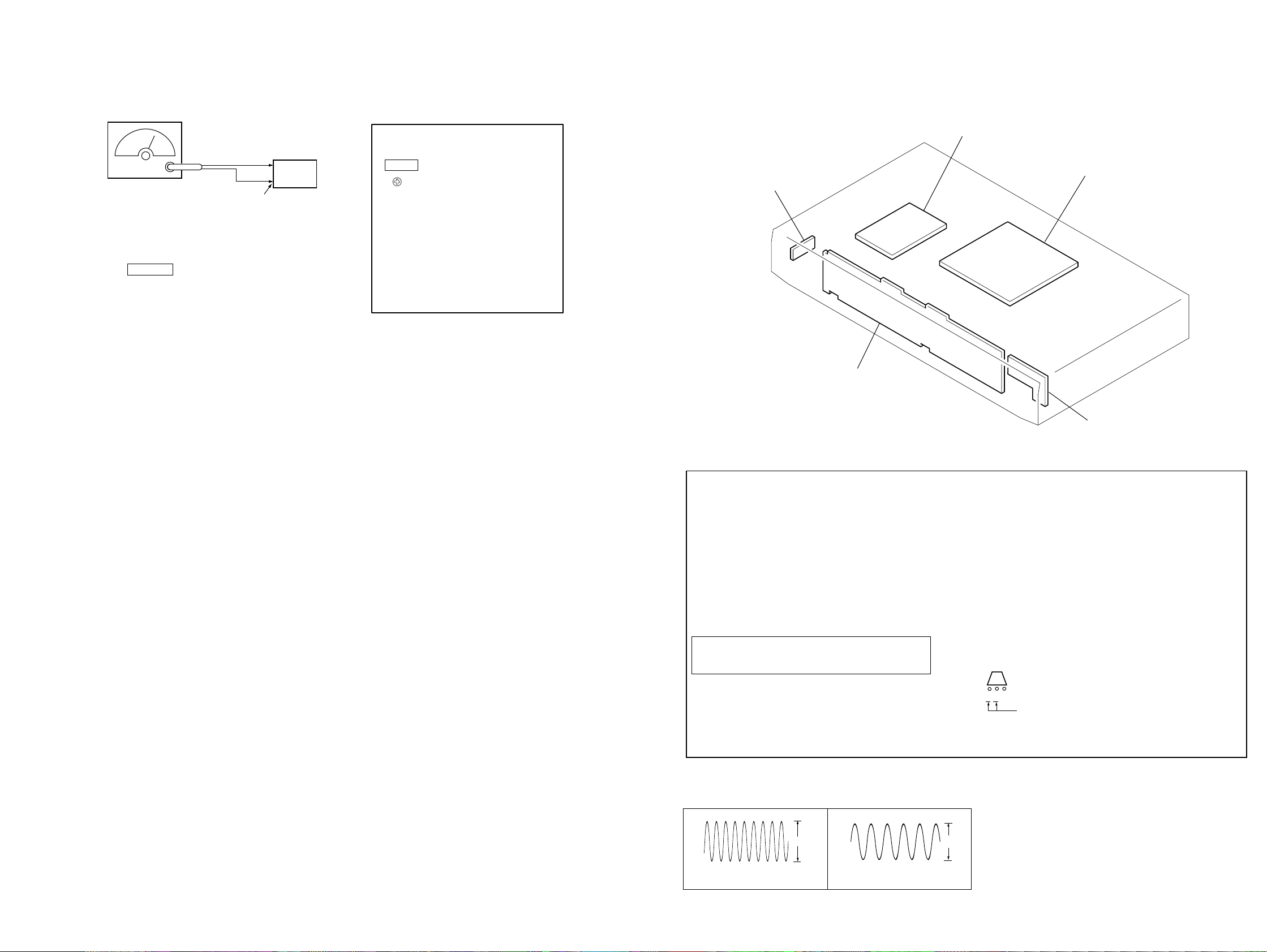
SECTION 3
AC SW board
ENCODER board
TRANSFORMER board
DISPLAY board
TUNER board
4.3Vp-p
4.19MHz
ELECTRICAL ADJUSTMENTS
SECTION 4
DIAGRAMS
FM Signal Level Adjustment
FM RF signal
generator
set
Carrier frequency : 98 MHz
Modulation : 1 kHz, 40 kHz deviation
Output level : 6.3 mV (76dBµ)
(75 Ω open)
FM ANTENNA
75 Ω coaxial
(TB101)
Procedure:
1. Tune the set to 98 MHz.
2. Push the DISPLAY button for digital signal meter indication.
3. Adjust RV201 to the place where level and “70dB M” indication lights on fluorescent indicator tube.
Adjustment Location:
[TUNER BOARD] — Component Side —
IC201
RV201
FM SIGNAL LEVEL
4-1. CIRCUIT BOARDS LOCATION
THIS NOTE IS COMMON FOR PRINTED WIRING
BOARDS AND SCHEMATIC DIAGRAMS.
(In addition to this, the necessary note is printed
in each block.)
For schematic diagrams.
Note:
• All capacitors are in µF unless otherwise noted. pF: µµF
50 WV or less are not indicated except for electrolytics
and tantalums.
• All resistors are in Ω and 1/
specified.
• 2 : nonflammable resistor.
• C : panel designation.
Note: The components identified by mark 0 or dotted line
with mark 0 are critical for safety.
Replace only with part number specified.
• U : B+ Line.
• V : B– Line.
• H : adjustment for repair.
• Voltages and waveforms are dc with respect to ground
under no-signal (detuned) conditions.
no mark : FM
: Can not be measured.
∗
4
W or less unless otherwise
WAVEFORMS
• Voltages are taken with a V OM (Input impedance 10 MΩ).
Voltage variations may be noted due to normal production tolerances.
• Waveforms are taken with a oscilloscope.
Voltage variations may be noted due to normal production tolerances.
• Circled numbers refer to waveforms.
• Signal path.
F : FM
For printed wiring boards.
Note:
• X : parts extracted from the component side.
• x : parts mounted on the conductor side.
• b : Pattern from the side which enables seeing.
• Indication of transistor
C
EB
These are omitted
1
4.8Vp-p
4.332MHz
IC802 qf
5
5
2
IC701 qs
Page 6

ST-SE520
4-2. SCHEMATIC DIAGRAM – TUNER SECTION –
• See page 5 for Waveform.
• See page 11 for IC Block Diagram.
(Page 8) (Page 8)
6
6
Page 7

4-3. PRINTED WIRING BOARD –TUNER SECTION –
• See page 5 for Circuit Boards Location.
ST-SE520
• Semiconductor Location
Ref. No. Location
D201 A-5
D901 B-5
D902 B-5
D903 C-5
D904 C-5
D905 C-4
D906 D-5
D907 C-3
D908 C-3
Ref. No. Location
IC201 B-1
IC302 A-4
IC802 D-3
IC901 C-3
Q301 A-3
Q302 A-2
Q303 A-3
Q304 A-3
Q702 D-1
Q901 C-2
(Page 9)
(Page 9)
7
7
Page 8

ST-SE520
4-4. SCHEMATIC DIAGRAM – DISPLAY SECTION –
• See page 5 for Waveform.
• See page 10 for IC Pin function.
(Page 6)
(Page 6)
PIN
FUNCTION
8
8
Page 9

4-5. PRINTED WIRING BOARD – DISPLAY SECTION –
• See page 5 for Circuit Boards Location.
ST-SE520
(Page 7)
(Page 7)
9
9
Page 10

4-6. IC PIN FUNCTION
• IC701 System Control (µPD78205GF-040-3BA)
10
11
12
13
14
15
16
17
18
19
20
21
22
23
24
25
26
27
28
29
30
31
32
33
34
35
36
37
38
39
40
1
2
3
4
5
6
7
8
9
Pin Name
VDD
ANT
ANT
BAND 1
BAND 2
IF-B
NC
MONO
TUN
RESET
X2
4.19MHz
GND
NC
LOCK
VDD
CLK
DA TA
D-IN
CE
BLN
ST
CAL
AST
AVSS
MUTE
E ON
PGM
DATA RDS
R2
KEY 2
KEY 1
SI
AVDD
AVREF
R IN
R 1
RDS CLK
POWER
GND
I/O Function
Power supply (+5V)
—
Not used
—
—
Not used
Not used
—
Not used
—
—
Not used
Not used
—
Not used
—
—
Not used
System reset input
I
Oscillation signal output (4.19MHz)
O
I
Oscillation signal output (4.19MHz)
Ground
—
Not used
—
I
Lock signal input
Power supply (+5V)
—
PLL clock to TB101
O
O
PLL data to TB101
PLL clock from TB101
I
PLL Latch to TB101
O
—
Not used.
I
Stereo display detection.
Not used
—
I
Auto stop signal detection
—
Ground
Muting signal output
O
O
External control
—
Not used
RDS data input
I
O
Rotary encoder phase detection
I
Key input
Key input
I
I
Signal input
—
Analog power supply (+5V)
Reference voltage (+5V)
I
I
Remote control input
I
Rotary encoder number of rotation detection
RDS data clock input
I
I
Power supply ON/OFF monitor
—
Ground
Pin No.
41
42
43
44
45
46
47 to 78
79
80 to 84
85
86 to 100
• Abbreviation
FL: FLUORESCENT INDICATOR TUBE
Pin Name
IS 5
IS 4
IS 3
IS 2
IS 1
VDD
P1 to P32
V LOAD
P33 to P37
G16
G15 to G1
I/O
I
I
Model detection
I
I
I
Power supply (+5V)
—
FL segment output
O
Power supply (–30V)
—
FL segment output
O
Not used
—
FL grid output
O
Function
10
10
Page 11

4-7. IC BLOCK DIAGRAMS
D
• T uner section
IC201 LA1235
MUTING
CIRCUIT
LEVEL
DET
NULL METER
FM IF AMP
LIMITER
3 6
2 5 81 4
IC802 BU1922
RDCL
1415 12 91016 13
METER
DRIVE
IF OFF
SHORTING
GND
QUADRATURE
TS7
IC901 LA5667
11
B+
DETUNE
DET
AF/NULL
DET
AF AMP
OSCO
141516 13 12 11 10 9
METER
OSCI
7
DDD
V
REG
GND
1 234
VSSD
TEST
CONTROL
REG
567
TSTL
QUAL
QUALITY BIT
GENERATOR
DEFFERENTIAL
DECODER
RDDA
TEST LOGIC AND OUTPUT
SELECTOR SWITCH
OSCILLATOR
AND
DIVIDER
BIPHASE
SYMBOL
DECODER
321 4 5 6 7 8
Vref
RECONSTRUCTION
FILTER
MUX
DDA
V
57kHz
BANDPASS
(8th ORDER)
CONTAS LOOP
VARIABLE AND
FIXED DIVIDER
CLOCK REGENERATION
AND SYNC
REFERENCE
VOLTAGE
VSSA
VP1
ANTI-
ALIASING
FILTER
CLOCKED
COMPARATOR
CIN
SCOUT
11
Page 12

SECTION 5
)
EXPLODED VIEW
NOTE:
• Items marked “*” are not stocked since they are
seldom required for routine service. Some delay
should be anticipated when ordering these items.
• Color Indication of Appearance Parts Example:
KNOB, BALANCE (WHITE)
X
Cabinets color
12
10
24
20
5
11
26
6
FL701
Supplied
7
with RV701
7
• The mechanical parts with no reference number in
the exploded views are not supplied.
• Accessories and packing materials are given in the
last of this parts list.
13
12
23
29
19
12
28
20
14
26
20
15
14
The components identified by
mark 0 or dotted line with mark
0 are critical for safety.
Replace only with part number
specified.
25
PC901(UK)
23
18
22
PC901(AEP
21
20
9
8
23
3
2
1
Ref. No. Part No. Description Remark
1 4-997-882-01 KNOB (T)(BLACK)
1 4-997-882-11 KNOB (T)(SILVER)
2 X-4949-582-2 PANEL ASSY, FRONT (BLACK)
2 X-4949-583-2 PANEL ASSY, FRONT (SILVER)
3 4-977-593-01 RING (DIA. 50), ORNAMENTAL
4 4-977-358-31 CUSHION
5 3-931-429-71 BUTTON (POWER)(BLACK)
5 3-931-429-81 BUTTON (POWER)(SILVER)
* 6 1-668-814-11 AC SW BOARD
7 4-981-264-01 BUTTON (4)(BLACK)
7 4-981-264-21 BUTTON (4)(SILVER)
8 4-997-881-01 ESCUTCHEON (BLACK)
8 4-997-881-11 ESCUTCHEON (SILVER)
* 9 1-668-815-11 ENCODER BOARD
* 10 A-4407-375-A DISPLAY BOARD, COMPLETE
4
17
27
23
16
23
Ref. No. Part No. Description Remark
* 14 3-346-265-31 HOLDER, PC BOARD
* 15 3-697-679-01 CUSHION, LS
16 X-4947-124-1 FOOT ASSY (F50150S)(SILVER)
16 X-4947-207-1 FOOT ASSY (F50150S)(BLACK)
* 17 4-215-931-01 PANEL, BACK (AEP)
17 4-215-931-51 PANEL, BACK (UK)
18 3-703-244-00 BUSHING, CORD
* 19 A-4407-374-A TUNER BOARD, COMPLETE
20 4-951-620-01 SCREW (2.6X8), +BVTP
21 3-703-685-21 SCREW (+BV 3X8)
22 3-704-515-31 SCREW (BV/RING)
23 7-685-646-79 SCREW +BVTP 3X8 TYPE2 IT-3
24 4-963-404-21 EMBLEM (5-A), SONY
25 1-773-002-11 WIRE (FLAT TYPE)(15 CORE)
* 26 4-921-941-01 CUSHION (FL)
* 11 4-945-292-01 HOLDER, INDICATION TUBE
12 3-710-901-01 SCREW, TAPPING (SILVER)
12 3-710-901-11 SCREW, TAPPING (BLACK)
* 13 4-978-901-41 CASE (407026)(BLACK)
* 13 4-985-744-01 CASE (407026)(SILVER)
12
27 1-693-410-21 TUNER (PACK)
* 28 3-669-610-00 SPACER
* 29 1-668-816-11 TRANSFORMER BOARD
FL701 1-517-177-21 INDICATOR TUBE, FLUORESCENT
0 PC901 1-575-651-21 CORD, POWER (AEP)
0 PC901 1-751-523-11 CORD, POWER (UK)
Page 13

SECTION 6
ELECTRICAL PARTS LIST
Note:
The components identified by
mark 0 or dotted line with mark
0 are critical for safety.
Replace only with part number
specified.
When indicating parts by reference
number, please include the board
name.
Ref. No. Part No. Description Remark Ref. No. Part No. Description Remark
* 1-668-814-11 AC SW BOARD
***********
< CAPACITOR >
0 C951 1-113-915-11 CERAMIC 0.001uF 20% 250V
< SWITCH >
0 S901 1-572-267-51 SWITCH, PUSH (AC POWER)(1 KEY)(!)
**************************************************************
* A-4407-375-A DISPLAY BOARD, COMPLETE
***********************
* 4-921-941-01 CUSHION (FL)
* 4-945-292-01 HOLDER, INDICATION TUBE
7-685-872-09 SCREW +BVTT 3X8 (S)
< CAPACITOR >
C701 1-162-306-11 CERAMIC 0.01uF 20% 16V
C702 1-162-306-11 CERAMIC 0.01uF 20% 16V
C703 1-162-209-31 CERAMIC 27PF 5% 50V
C704 1-162-209-31 CERAMIC 27PF 5% 50V
C705 1-162-306-11 CERAMIC 0.01uF 20% 16V
C706 1-164-159-21 CERAMIC 0.1uF 50V
C707 1-126-947-11 ELECT 47uF 20% 35V
C708 1-162-306-11 CERAMIC 0.01uF 20% 16V
C709 1-162-306-11 CERAMIC 0.01uF 20% 16V
C710 1-162-306-11 CERAMIC 0.01uF 20% 16V
C711 1-126-964-11 ELECT 10uF 20% 50V
C712 1-104-905-11 CAPACITOR 0.22F 5.5V
C713 1-162-306-11 CERAMIC 0.01uF 20% 16V
C714 1-126-959-11 ELECT 0.47uF 20% 50V
C717 1-162-286-21 CERAMIC 220PF 10% 50V
< DIODE >
• Due to standardization, replacements in the parts list
may be different from the parts specified in the
diagrams or the components used on the set.
• -XX, -X mean standardized parts, so they may have
some difference from the original one.
• Items marked “*” are not stocked since they are
seldom required for routine service. Some delay
should be anticipated when ordering these items.
• RESISTORS
All resistors are in ohms
METAL: Metal-film resistor
METAL OXIDE: Metal Oxide-film resistor
F : nonflammable
Q701 8-729-119-78 TRANSISTOR 2SC2785-HFE
R701 1-249-437-11 CARBON 47K 5% 1/4W
R703 1-249-429-11 CARBON 10K 5% 1/4W
R704 1-249-419-11 CARBON 1.5K 5% 1/4W F
R705 1-249-419-11 CARBON 1.5K 5% 1/4W F
R707 1-249-441-11 CARBON 100K 5% 1/4W
R708 1-249-441-11 CARBON 100K 5% 1/4W
R709 1-247-807-31 CARBON 100 5% 1/4W
R710 1-249-406-11 CARBON 120 5% 1/4W F
R711 1-249-406-11 CARBON 120 5% 1/4W F
R712 1-249-407-11 CARBON 150 5% 1/4W F
R713 1-249-408-11 CARBON 180 5% 1/4W F
R714 1-247-815-91 CARBON 220 5% 1/4W
R715 1-249-410-11 CARBON 270 5% 1/4W F
R716 1-249-411-11 CARBON 330 5% 1/4W
R717 1-249-413-11 CARBON 470 5% 1/4W F
R718 1-249-414-11 CARBON 560 5% 1/4W F
R719 1-249-416-11 CARBON 820 5% 1/4W F
R720 1-249-418-11 CARBON 1.2K 5% 1/4W F
R721 1-249-421-11 CARBON 2.2K 5% 1/4W F
R722 1-249-424-11 CARBON 3.9K 5% 1/4W F
R724 1-247-807-31 CARBON 100 5% 1/4W
R725 1-249-406-11 CARBON 120 5% 1/4W F
R726 1-249-406-11 CARBON 120 5% 1/4W F
R727 1-249-407-11 CARBON 150 5% 1/4W F
R728 1-249-408-11 CARBON 180 5% 1/4W F
R729 1-247-815-91 CARBON 220 5% 1/4W
R730 1-249-410-11 CARBON 270 5% 1/4W F
R731 1-249-411-11 CARBON 330 5% 1/4W
R732 1-249-413-11 CARBON 470 5% 1/4W F
0 R733 1-249-414-11 CARBON 560 5% 1/4W F
• SEMICONDUCTORS
• CAPACITORS
• COILS
< TRANSISTOR >
< RESISTOR >
AC SW
In each case, u: µ , for example:
uA...: µ A..., uPA...: µ PA..., uPB...: µ PB...,
uPC...: µ PC..., uPD...: µ PD...
uF : µ F
uH : µ H
DISPLAY
D701 8-719-991-33 DIODE 1SS133T-77
D702 8-719-991-33 DIODE 1SS133T-77
D703 8-719-991-33 DIODE 1SS133T-77
D705 8-719-991-33 DIODE 1SS133T-77
D707 8-719-991-33 DIODE 1SS133T-77
< FLUORESCENT INDICATOR >
FL701 1-517-177-21 INDICATOR TUBE, FLUORESCENT
< IC >
IC701 8-759-495-96 IC uPD780205GF-040-3BA
IC702 8-749-014-66 IC NJL64H400A
R734 1-249-416-11 CARBON 820 5% 1/4W F
R735 1-249-418-11 CARBON 1.2K 5% 1/4W F
R736 1-247-807-31 CARBON 100 5% 1/4W
R738 1-249-401-11 CARBON 47 5% 1/4W F
R739 1-249-417-11 CARBON 1K 5% 1/4W F
R740 1-247-863-91 CARBON 22K 5% 1/4W
R741 1-247-895-91 CARBON 470K 5% 1/4W
R742 1-249-413-11 CARBON 470 5% 1/4W F
R743 1-249-413-11 CARBON 470 5% 1/4W F
R744 1-249-413-11 CARBON 470 5% 1/4W F
R745 1-249-413-11 CARBON 470 5% 1/4W F
R746 1-249-413-11 CARBON 470 5% 1/4W F
13
Page 14

DISPLAY
Ref. No. Part No. Description Remark Ref. No. Part No. Description Remark
R747 1-249-413-11 CARBON 470 5% 1/4W F
R749 1-249-413-11 CARBON 470 5% 1/4W F
R750 1-249-413-11 CARBON 470 5% 1/4W F
R751 1-249-413-11 CARBON 470 5% 1/4W F
R752 1-249-413-11 CARBON 470 5% 1/4W F
R753 1-249-413-11 CARBON 470 5% 1/4W F
R754 1-249-413-11 CARBON 470 5% 1/4W F
ENCODER
TRANSFORMER TUNER
< CONNECTOR >
CNP901 1-580-230-11 PIN, CONNECTOR (PC BOARD) 2P
CNP951 1-564-321-00 PIN, CONNECTOR 2P
< LEAD >
ECP900 1-690-880-51 LEAD (WITH CONNECTOR)
< SWITCH >
S701 1-554-303-21 SWITCH, TACTILE (SHIFT)
S702 1-554-303-21 SWITCH, TACTILE (1)
S703 1-554-303-21 SWITCH, TACTILE (2)
S704 1-554-303-21 SWITCH, TACTILE (3)
S705 1-554-303-21 SWITCH, TACTILE (4)
S706 1-554-303-21 SWITCH, TACTILE (5)
S707 1-554-303-21 SWITCH, TACTILE (6)
S708 1-554-303-21 SWITCH, TACTILE (7)
S709 1-554-303-21 SWITCH, TACTILE (8)
S710 1-554-303-21 SWITCH, TACTILE (9)
S711 1-554-303-21 SWITCH, TACTILE (0)
S712 1-554-303-21 SWITCH, TACTILE (DIRECT)
S713 1-554-303-21 SWITCH, TACTILE (MENU)
S714 1-554-303-21 SWITCH, TACTILE (RETURN)
S717 1-554-303-21 SWITCH, TACTILE (DISPLAY)
S718 1-554-303-21 SWITCH, TACTILE (PTY)
S719 1-554-303-21 SWITCH, TACTILE (EON NEWS/INFO)
S720 1-554-303-21 SWITCH, TACTILE (EON TA )
S721 1-554-303-21 SWITCH, TACTILE (AUTO-BETICAL SELECT)
S722 1-554-303-21 SWITCH, TACTILE (MEMORY)
S723 1-554-303-21 SWITCH, TACTILE (FM MODE)
S724 1-554-303-21 SWITCH, TACTILE (BAND)
S727 1-554-303-21 SWITCH, TACTILE (CHARACTER)
S728 1-554-303-21 SWITCH, TACTILE (TUNE MODE)
< TRANSFORMER >
0 PT901 1-423-525-11 TRANSFORMER, POWER
**************************************************************
* A-4407-374-A TUNER BOARD, COMPLETE
*********************
1-690-880-41 LEAD (WITH CONNECTOR)
< CAPACITOR >
C101 1-162-306-11 CERAMIC 0.01uF 20% 16V
C102 1-126-964-11 ELECT 10uF 20% 50V
C103 1-162-306-11 CERAMIC 0.01uF 20% 16V
C104 1-126-964-11 ELECT 10uF 20% 50V
C105 1-124-463-00 ELECT 0.1uF 20% 50V
C201 1-162-288-31 CERAMIC 330PF 10% 50V
C202 1-162-306-11 CERAMIC 0.01uF 20% 16V
C203 1-162-306-11 CERAMIC 0.01uF 20% 16V
C204 1-162-306-11 CERAMIC 0.01uF 20% 16V
C205 1-126-967-11 ELECT 47uF 20% 16V
C206 1-162-306-11 CERAMIC 0.01uF 20% 16V
C207 1-162-306-11 CERAMIC 0.01uF 20% 16V
C301 1-126-963-11 ELECT 4.7uF 20% 50V
C302 1-126-963-11 ELECT 4.7uF 20% 50V
C303 1-126-964-11 ELECT 10uF 20% 50V
< VIBRATOR >
X701 1-760-422-11 VIBRATOR, CRYSTAL (4.192MHz)
**************************************************************
* 1-668-815-11 ENCODER BOARD
*************
< RESISTOR >
R723 1-249-430-11 CARBON 12K 5% 1/4W
< VARIABLE RESISTOR >
RV701 1-475-696-11 ENCODER, ROTARY (TUNING/SELECT)
< SWITCH >
S715 1-554-303-21 SWITCH, TACTILE (ENTER)
**************************************************************
* 1-668-816-11 TRANSFORMER BOARD
*****************
< CAPACITOR >
C952 1-162-306-11 CERAMIC 0.01uF 20% 16V
C304 1-126-964-11 ELECT 10uF 20% 50V
C305 1-110-335-11 MYLAR 100PF 5% 50V
C306 1-110-335-11 MYLAR 100PF 5% 50V
C308 1-126-963-11 ELECT 4.7uF 20% 50V
C309 1-126-963-11 ELECT 4.7uF 20% 50V
C319 1-126-934-11 ELECT 220uF 20% 16V
C352 1-130-471-00 MYLAR 0.001uF 5% 50V
C353 1-130-471-00 MYLAR 0.001uF 5% 50V
C806 1-102-527-11 CERAMIC 82PF 5% 50V
C807 1-102-852-91 CERAMIC 47PF 5% 50V
C808 1-162-306-11 CERAMIC 0.01uF 20% 16V
C809 1-126-967-11 ELECT 47uF 20% 16V
C810 1-126-961-11 ELECT 2.2uF 20% 50V
C811 1-162-306-11 CERAMIC 0.01uF 20% 16V
C812 1-162-291-31 CERAMIC 560PF 10% 50V
C813 1-162-306-11 CERAMIC 0.01uF 20% 16V
C814 1-162-306-11 CERAMIC 0.01uF 20% 16V
C901 1-101-004-00 CERAMIC 0.01uF 50V
C902 1-101-004-00 CERAMIC 0.01uF 50V
C903 1-126-967-11 ELECT 47uF 20% 50V
C904 1-126-967-11 ELECT 47uF 20% 50V
C905 1-126-953-11 ELECT 2200uF 20% 35V
C906 1-126-969-11 ELECT 220uF 20% 50V
C907 1-126-935-11 ELECT 470uF 20% 6.3V
C908 1-126-964-11 ELECT 10uF 20% 50V
The components identified by mark 0 or dotted
line with mark 0 are critical for safety.
Replace only with part number specified.
14
Page 15

TUNER
Ref. No. Part No. Description Remark Ref. No. Part No. Description Remark
C909 1-126-967-11 ELECT 47uF 20% 16V
C910 1-126-964-11 ELECT 10uF 20% 50V
C911 1-126-959-11 ELECT 0.47uF 20% 50V
< CONNECTOR >
R310 1-247-815-91 CARBON 220 5% 1/4W
0 R316 1-249-405-11 CARBON 100 5% 1/4W F
R317 1-249-417-11 CARBON 1K 5% 1/4W F
R318 1-249-417-11 CARBON 1K 5% 1/4W F
0 R319 1-249-405-11 CARBON 100 5% 1/4W F
CN101 1-568-834-11 SOCKET, CONNECTOR 15P
CNJ203 1-566-212-11 PIN, CONNECTOR 3P (EON CONTROL OUT)
CNJ301 1-568-250-11 JACK, PIN 2P (LINE OUT)
* CNP701 1-568-936-11 PIN, CONNECTOR 9P
* CNP702 1-568-935-11 PIN, CONNECTOR 8P
CNP952 1-766-267-11 PIN, CONNECTOR (PC BOARD) 5P
< DIODE >
D201 8-719-991-33 DIODE 1SS133T-77
D901 8-719-200-82 DIODE 11ES2
D902 8-719-200-82 DIODE 11ES2
D903 8-719-200-82 DIODE 11ES2
D904 8-719-200-82 DIODE 11ES2
D905 8-719-110-69 DIODE RD27ES-B4
D906 8-719-109-97 DIODE RD6.8ES-B2
D907 8-719-200-82 DIODE 11ES2
D908 8-719-991-33 DIODE 1SS133T-77
< IC >
IC201 8-759-812-35 IC LA1235
IC302 8-759-634-51 IC M5218AP
IC802 8-759-450-86 IC BU1922
IC901 8-759-820-09 IC LA5667
< COIL >
L351 1-410-509-11 INDUCTOR 10uH
L352 1-410-509-11 INDUCTOR 10uH
0 R320 1-249-381-11 CARBON 100 5% 1/4W F
R331 1-247-815-91 CARBON 220 5% 1/4W
R332 1-247-815-91 CARBON 220 5% 1/4W
R333 1-249-417-11 CARBON 1K 5% 1/4W F
R334 1-249-417-11 CARBON 1K 5% 1/4W F
R361 1-249-437-11 CARBON 47K 5% 1/4W
R362 1-249-437-11 CARBON 47K 5% 1/4W
R806 1-249-421-11 CARBON 2.2K 5% 1/4W F
0 R807 1-249-401-11 CARBON 47 5% 1/4W F
R808 1-247-815-91 CARBON 220 5% 1/4W
R809 1-247-807-31 CARBON 100 5% 1/4W
R811 1-249-429-11 CARBON 10K 5% 1/4W
0 R812 1-249-405-11 CARBON 100 5% 1/4W F
0 R902 1-247-752-11 CARBON 1K 5% 1/2W F
R903 1-249-441-11 CARBON 100K 5% 1/4W
R904 1-249-437-11 CARBON 47K 5% 1/4W
R905 1-249-437-11 CARBON 47K 5% 1/4W
R906 1-249-437-11 CARBON 47K 5% 1/4W
R909 1-249-417-11 CARBON 1K 5% 1/4W F
R910 1-249-417-11 CARBON 1K 5% 1/4W F
R911 1-249-417-11 CARBON 1K 5% 1/4W F
R912 1-249-417-11 CARBON 1K 5% 1/4W F
< VARIABLE RESISTOR >
RV201 1-241-765-11 RES, ADJ, CARBON 22K
< VIBRATOR >
< TRANSISTOR >
Q301 8-729-922-37 TRANSISTOR 2SD2144S-UVW
Q302 8-729-922-37 TRANSISTOR 2SD2144S-UVW
Q303 8-729-922-37 TRANSISTOR 2SD2144S-UVW
Q304 8-729-922-37 TRANSISTOR 2SD2144S-UVW
Q702 8-729-119-78 TRANSISTOR 2SC2785-HFE
Q901 8-729-029-56 TRANSISTOR DTA144ESA
< RESISTOR >
0 R101 1-249-401-11 CARBON 47 5% 1/4W F
R104 1-249-429-11 CARBON 10K 5% 1/4W
R105 1-249-429-11 CARBON 10K 5% 1/4W
R201 1-249-413-11 CARBON 470 5% 1/4W F
0 R202 1-249-405-11 CARBON 100 5% 1/4W F
R203 1-249-393-11 CARBON 10 5% 1/4W F
R301 1-249-441-11 CARBON 100K 5% 1/4W
R302 1-249-441-11 CARBON 100K 5% 1/4W
R303 1-249-441-11 CARBON 100K 5% 1/4W
R304 1-249-441-11 CARBON 100K 5% 1/4W
R305 1-247-843-11 CARBON 3.3K 5% 1/4W
R306 1-247-843-11 CARBON 3.3K 5% 1/4W
R307 1-249-420-11 CARBON 1.8K 5% 1/4W F
R308 1-249-420-11 CARBON 1.8K 5% 1/4W F
R309 1-247-815-91 CARBON 220 5% 1/4W
X801 1-579-900-21 VIBRATOR, CRYSTAL (4.332MHz)
**************************************************************
MISCELLANEOUS
*************
25 1-773-002-11 WIRE (FLAT TYPE)(15 CORE)
27 1-693-410-21 TUNER (PACK)
FL701 1-517-177-21 INDICATOR TUBE, FLUORESCENT
0 PC901 1-575-651-21 CORD, POWER (AEP)
0 PC901 1-751-523-11 CORD, POWER (UK)
**************************************************************
ACCESSORIES & PACKING MATERIALS
*******************************
1-501-594-11 ANTENNA (FM)
1-501-721-11 ANTENNA (LOOP)
1-558-271-11 CORD, CONNECTION (AUDIO, 108cm)
1-765-383-11 CORD (WITH CONNECTOR)
3-865-569-12 MANUAL, INSTRUCTION
(ENGLISH,FRENCH,SPANISH,PORTUGUESE)(AEP,UK)
3-865-569-22 MANUAL, INSTRUCTION
(GERMAN,DUTCH,SWEDISH,ITALIAN)(AEP)
3-865-569-32 MANUAL,INSTRUCTION (DANISH,FINNISH)(AEP)
The components identified by mark 0 or dotted
line with mark 0 are critical for safety.
Replace only with part number specified.
15
Page 16

ST-SE520
9-922-832-12
16
Sony Corporation
Home Audio Division Company
Printed in Hungary © 2000. 4
2000D097511-1
Published by Quality Assurance Dept.
 Loading...