Sony STSDB-900 Service manual
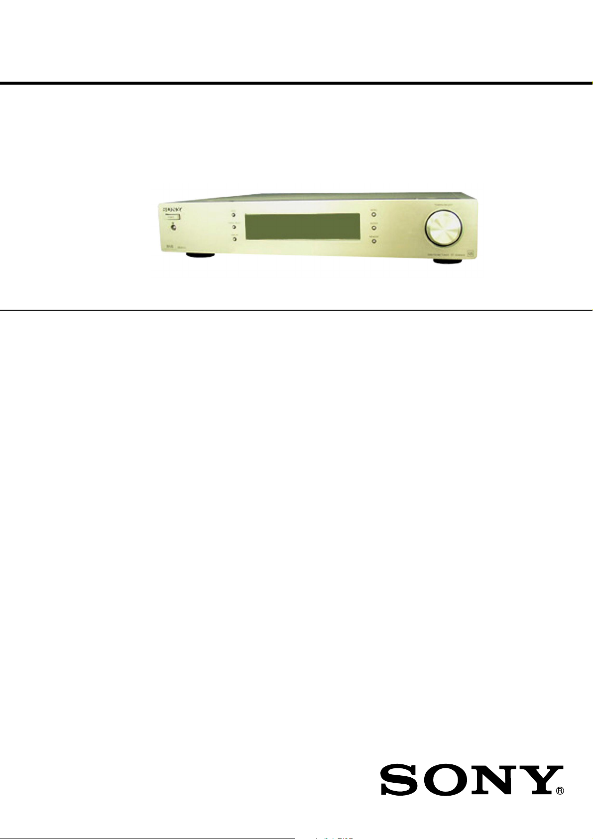
ST-SDB900
SERVICE MANUAL
Ver 1.0 2004.07
Manufactured under license from Dolby Laboratories.
“Dolby”, “Pro Logic” and the double-D symbol are
trademarks of Dolby Laboratories.
“DTS” and “DTS Digital Surround” are trademarks of Digital
Theater Systems, Inc.
SPECIFICATIONS
AEP Model
UK Model
DAB tuner section
Frequency range 174.928 (5A) – 239.200 (13F) MHz
For details, see “DAB frequency table”
below.
Sensitivity –99 dBm
Signal-to-noise ratio 97 dB
THD+N 0.009% (1 kHz)
Channel separation 87 dB (1 kHz)
Selectivity 40 dB (at adjacent channel)
Frequency response +0.5/–0.5 dB (5 Hz – 20 kHz)
Digital output Optical
Sampling frequency:
48 kHz
Aerial terminal 75 Ω, F female
Analog output level 2 Vrms
FM tuner section
Frequency range 87.5 – 108.0 MHz (50 kHz step)
IHF Sensitivity 1.0 µV
Signal-to-noise ratio at 40 kHz deviation 70 dB (stereo)
THD+N 1 kHz, 40 kHz deviation 0.5% (stereo)
Channel separation 45 dB (1 kHz)
Selectivity at 400 kHz 60 dB
Frequency response +0.5/–2.0 dB (30 Hz – 15 kHz)
Aerial terminal 75 Ω, IEC male
AM tuner section
Frequency range 531 – 1,602 kHz (9 kHz step)
Sensitivity (with AM loop aerial)
330 µV/m
Signal-to-noise ratio 54 dB
THD+N 0.5% (400 Hz)
Selectivity at 9 kHz 35 dB
Aerial terminal Push lever
General
Power requirements 230 V AC, 50/60 Hz
Power consumption 12 W
Dimensions 430 x 85 x 300 mm (w/h/d)
Weight 4.5 kg
Remote control capabilityIR
Station preset capacity DAB maximum of 99
FM maximum of 30
AM maximum of 30
Supplied accessories
• Audio cord (1)
• AM loop aerial (1)
• FM wire aerial (1)
• DAB wire aerial (1)
• Remote commander (1)
• R6 (size AA) batteries (2)
Design and specifications are subject to change without notice.
9-879-012-01
2004G0278-1
© 2004.07
DAB/FM/AM TUNER
Sony Corporation
Home Audio Company
Published by Sony Engineering Corporation

ST-SDB900
DAB frequency table
Band-III (174 to 240 MHz)
Frequency Label Frequency Label
174.928MHz 5A 209.936MHz 10A
176.640MHz 5B 211.648MHz 10B
178.352MHz 5C 213.360MHz 10C
180.064MHz 5D 215.072MHz 10D
181.936MHz 6A 216.928MHz 11A
183.648MHz 6B 218.640MHz 11B
185.360MHz 6C 220.352MHz 11C
187.072MHz 6D 222.064MHz 11D
188.928MHz 7A 223.936MHz 12A
190.640MHz 7B 225.648MHz 12B
192.352MHz 7C 227.360MHz 12C
194.064MHz 7D 229.072MHz 12D
195.936MHz 8A 230.784MHz 13A
197.648MHz 8B 232.496MHz 13B
199.360MHz 8C 234.208MHz 13C
201.072MHz 8D 235.776MHz 13D
202.928MHz 9A 237.488MHz 13E
204.640MHz 9B 239.200MHz 13F
206.352MHz 9C
208.064MHz 9D
TABLE OF CONTENTS
1. GENERAL ................................................................... 3
2. TEST MODE ............................................................... 4
3. DIAGRAMS
3-1. Block Diagram ................................................................ 9
3-2. Printed Wiring Board – MAIN Board (Side A) –............ 10
3-3. Printed Wiring Board – MAIN Board (Side B) –............ 11
3-4. Schematic Diagram – MAIN Board (1/3) – .................... 12
3-5. Schematic Diagram – MAIN Board (2/3) – .................... 13
3-6. Schematic Diagram – MAIN Board (3/3) – .................... 14
3-7. Printed Wiring Board
– TRANS, AC SW, JOG, RM Board –............................ 15
3-8. Printed Wiring Board – DISPLAY Board – .................... 16
3-9. Schematic Diagram – DISPLAY Board – ....................... 17
4. EXPLODED VIEWS
4-1. Case, Front Panel Section................................................ 20
4-2. Chassis Section................................................................ 21
5. ELECTRICAL PARTS LIST .................................. 22
* This tuner does not support L-Band reception.
SAFETY-RELATED COMPONENT WARNING!!
COMPONENTS IDENTIFIED BY MARK 0 OR DOTTED LINE
WITH MARK 0 ON THE SCHEMATIC DIAGRAMS AND IN THE
PARTS LIST ARE CRITICAL TO SAFE OPERATION. REPLACE
THESE COMPONENTS WITH SONY PARTS WHOSE P AR T NUMBERS APPEAR AS SHOWN IN THIS MANUAL OR IN SUPPLEMENTS PUBLISHED BY SONY.
Unleaded solder
Boards requiring use of unleaded solder are printed with the leadfree mark (LF) indicating the solder contains no lead.
(Caution: Some printed circuit boards may not come printed with
the lead free mark due to their particular size.)
: LEAD FREE MARK
Unleaded solder has the following characteristics.
• Unleaded solder melts at a temperature about 40°C higher than
ordinary solder.
Ordinary soldering irons can be used but the iron tip has to be
applied to the solder joint for a slightly longer time.
Soldering irons using a temperature regulator should be set to
about 350°C.
Caution: The printed pattern (copper foil) may peel away if the
heated tip is applied for too long, so be careful!
• Strong viscosity
Unleaded solder is more viscous (sticky, less prone to flow)
than ordinary solder so use caution not to let solder bridges
occur such as on IC pins, etc.
• Usable with ordinary solder
It is best to use only unleaded solder but unleaded solder may
also be added to ordinary solder.
Notes on chip component replacement
• Never reuse a disconnected chip component.
• Notice that the minus side of a tantalum capacitor may be damaged by heat.
2
SECTION 1
GENERAL
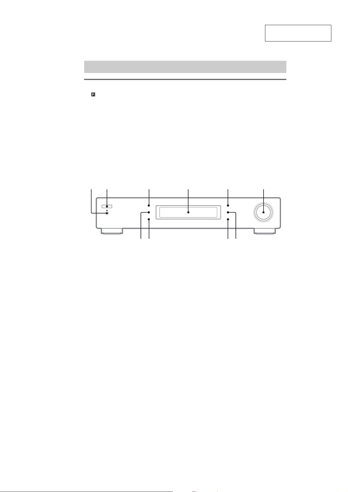
List of button locations and reference pages
Main unit
1 (remote sensor)
2 POWER switch
3 BAND
4 Display window
5 MENU
6 TUNING/SELECT
7 ENTER
8 MEMORY
9 DISPLAY
q; TUNING MODE
ST-SDB900
This section is extracted
from instruction manual.
1
2
q;
6534
89
7
3
ST-SDB900
SECTION 2
TEST MODE
1. Entering test mode
1. Turn OFF the power.
2. While pressing [DISPLAY] button and [MENU] button together, turn ON the [POWER] button.
3. When test mode starts “DIAG MENU” is displayed for a few seconds, then test mode starts.
[ FACTORY RESET ]
2. Leaving test mode
1. Turn OFF the power.
3. Selecting the test mode
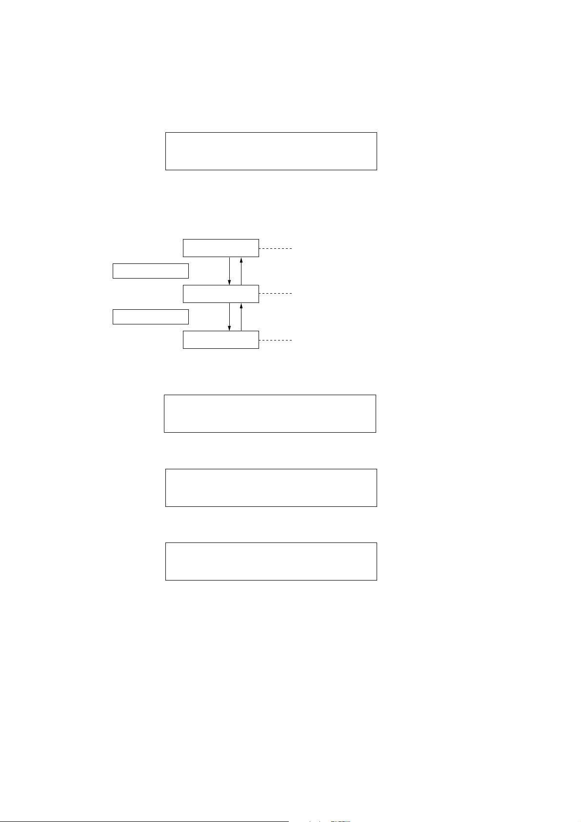
When you enter test mode, if you turn the [TUNING/SELECT] JOG dial, this switches the display to the test menu.
FACTORY RESET
TUNING/SELECT
TUNING/SELECT
3-1. Restoring the factory settings
1. Enter test mode, then turn the [TUNING/SELECT] dial to display “FACTORY RESET”.
dial
FL/KEY TEST
dial
VERSION
Screen display
Restores the factory settings
Fluorescent lamp display and button test
Version display
[ FACTORY RESET ]
2. Press the [ENTER] button. The “Executing” display.
Screen display
[ FACTORY RESET ]
Executing
3. After 3-4 seconds, the “Executing” disappears. Factory Reset is completed.
Screen display
[Contents of factory settings]
• BAND ................. DAB
• DAB Module ................. Service List Clear
................. DRC Off
................. DAB preset all clear
• FM Mode ................. STEREO
• 30 FM Preset ................. All 87.50 MHz
• 30 AM Preset ................. All 531 kHz
• Preset Station Name........ All clear
• DIMMER Full (duty 100)
4
[ FACTORY RESET ]
ST-SDB900
3-2. FL/KEY TEST MODE
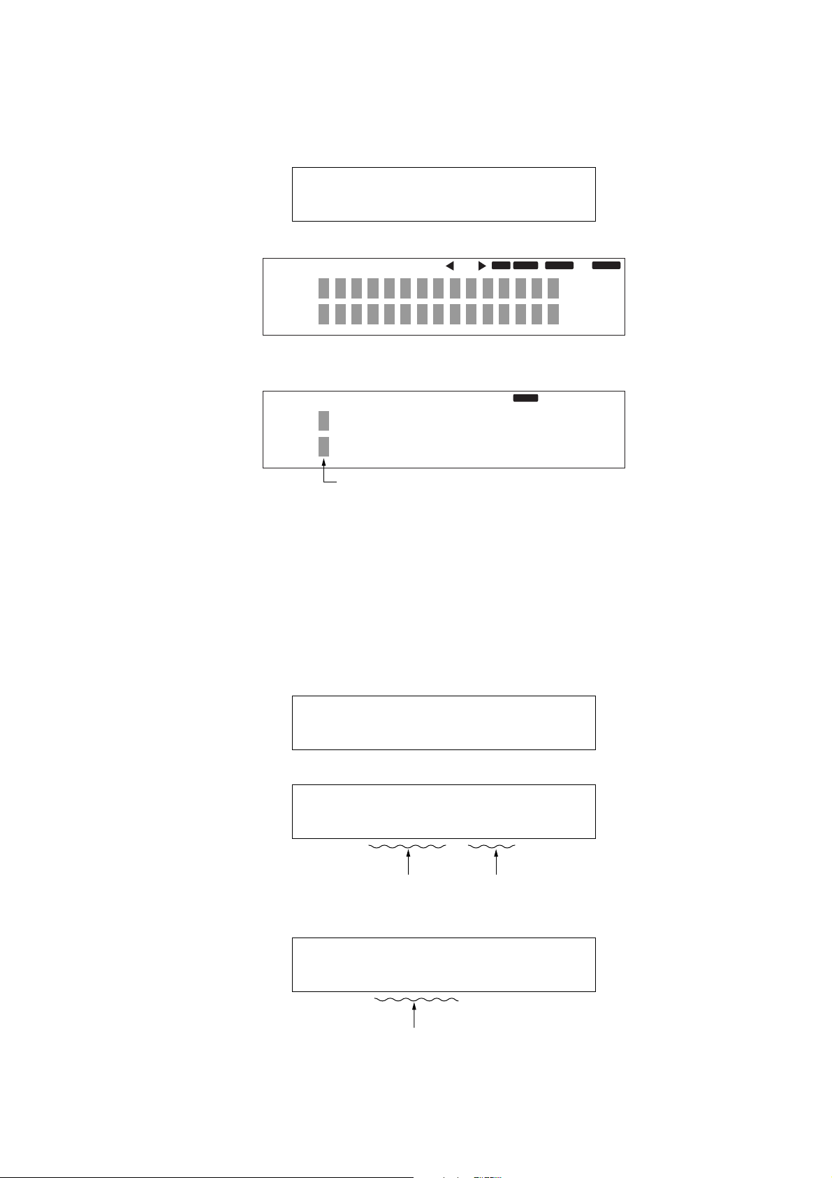
1. Enter test mode, then turn the [TUNING/SELECT] dial to display “FL/KEY TEST”.
Screen display
[ FL / KEY TEST ]
2. Press the [ENTER] button. The entire screen lights up.
Screen display
PTY
PTY
MEMORY
SECONDARYRDS TP STEREO
DAB
FM
AM
MONO
DUAL DRC
TUNED
AUTO
MANUALPRESET
3. Turning the [TUNING/SELECT] dial displays the dial check screen. When you turn the [TUNING/SELECT] dial left and right, the character
display moves left and right.
Screen display
TP
DAB
AM
MONO
DRC
TUNED
PRESET
Character display
4. To check operation of each button, press it and verify that the corresponding display goes out.
[BAND] button ................. “TP” display
[TUNING MODE] button..... “MONO” display
[DISPLAY] button .............. “DRC” display
[MENU] button ................. “TUNED” display
[ENTER] button ................. “PRESET” display
[MEMORY] button.............. “PTY” display
5. Press the [DAB] button on remote control after checking front panel button, “O” and “K” light up on a character display.
6. Turn OFF the power.
3-3. VERSION display
1. Enter test mode, then turn the [TUNING/SELECT] dial to display “VERSION”.
Screen display
[ VERSION ]
2. Press the [ENTER] button. The System Version is displayed.
Screen display
[ VERSION ]
sys v1.03 4415
Syscon Firmware
Version
3. Turn the [TUNING/SELECT] to the right to display the DAB version.
Screen display
Check sum
[ VERSION ]
dev v1.8 - 3
DAB Module Firmware Version
Turn the [TUNING/SELECT] dial to the left to display the System Version.
4. Press the [ENTER] button to return to test mode.
5
ST-SDB900
4. Temporary PRESET setting mode
This device is not adjusted but reception can be checked with the temporary Preset values.
1. Turn OFF the power.
2. While pressing [DISPLAY] button and [MEMORY] button together, turn ON [POWER] button.
3. When you enter temporary PRESET setting mode, the “MEMORY” display flashes. The only dif ference in this mode is the use of t he
temporary Preset values. Otherwise, operation is normal.
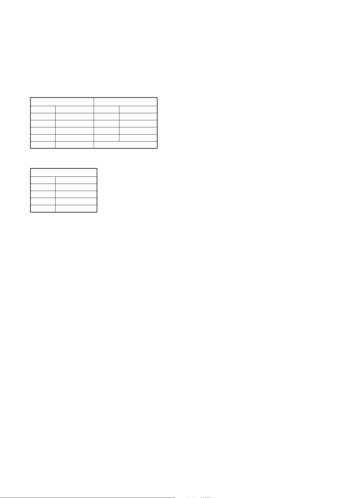
4. For the FM and AM band, the PRESET values are as follows.
FM band AM band
FM01 87.50 MHz AM01 531 kHz
FM02 88.00 MHz AM02 603 kHz
FM03 98.00 MHz AM03 999 kHz
FM04 100.00 MHz AM04 1404 kHz
FM05 106.00 MHz AM05 1602 kHz
FM06 108.00 MHz –
5. For the DAB band, there are no temporary Preset values.
Instead, the CH labels handle this with “MENU” - “DAB TUNE AID” as follows.
DAB band
5A (174.928 MHz)
5B (176.640 MHz)
8D (201.072 MHz)
12B (225.648 MHz)
13F (239.200 MHz)
6. End temporary PRESET mode with a Power OFF.
6
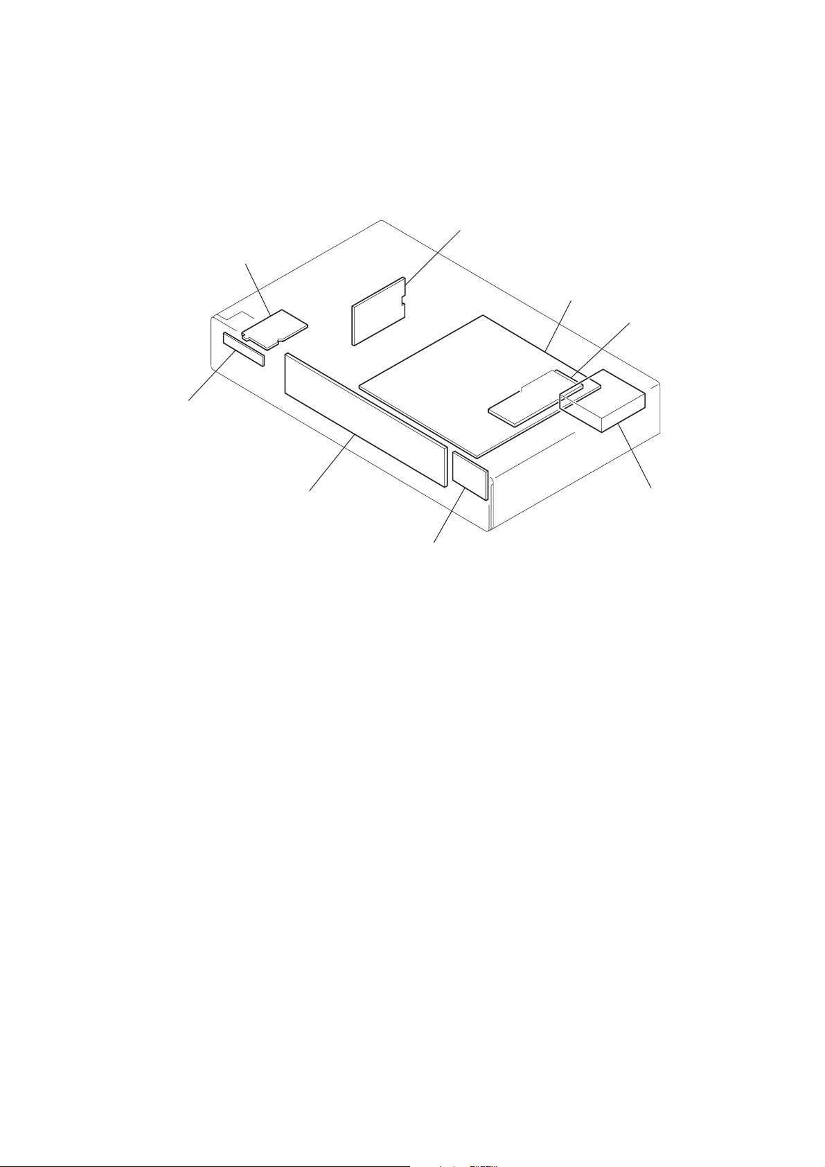
• Circuit Boards Location
AC SW board
RM board
ST-SDB900
SECTION 3
DIAGRAMS
TRANS board
MAIN board
DAB tuner module
DISPLAY board
tuner unit
JOG board
7
ST-SDB900
NOTE FOR PRINTED WIRING BOARDS AND SCHEMATIC DIAGRAMS
(In addition to this necessary note is printed in each block.)
Note on Schematic Diagram:
• All capacitors are in µF unless otherwise noted. (p: pF)
50 WV or less are not indicated except f or electrolytics and
tantalums.
• All resistors are in Ω and 1/
specified.
• % : indicates tolerance.
• f : internal component.
• 2 : nonflammable resistor.
• C : panel designation.
Note: The components identified by mark 0 or dotted
line with mark 0 are critical for safety.
Replace only with part number specified.
• A : B+ Line.
• B : B– Line.
•Voltages and w av ef orms are dc with respect to ground under no-signal conditions.
No mark : FM
•Voltages are tak en with a VOM (Input impedance 10 MΩ).
Voltage variations may be noted due to normal production
tolerances.
•Waveforms are taken with a oscilloscope.
Voltage variations may be noted due to normal production
tolerances.
• Circled numbers refer to waveforms.
• Signal path.
F : FM
g : ANALOG OUT
I : DIGITAL OUT
4
W or less unless otherwise
Note on Printed Wiring Board:
• X : parts extracted from the component side.
• a : Through hole.
• : Pattern from the side which enables seeing.
Caution:
Pattern face side: Parts on the parts face side seen from
(Side A) the parts face are indicated.
Parts face side: Parts on the pattern face side seen from
(Side B) the pattern face are indicated.
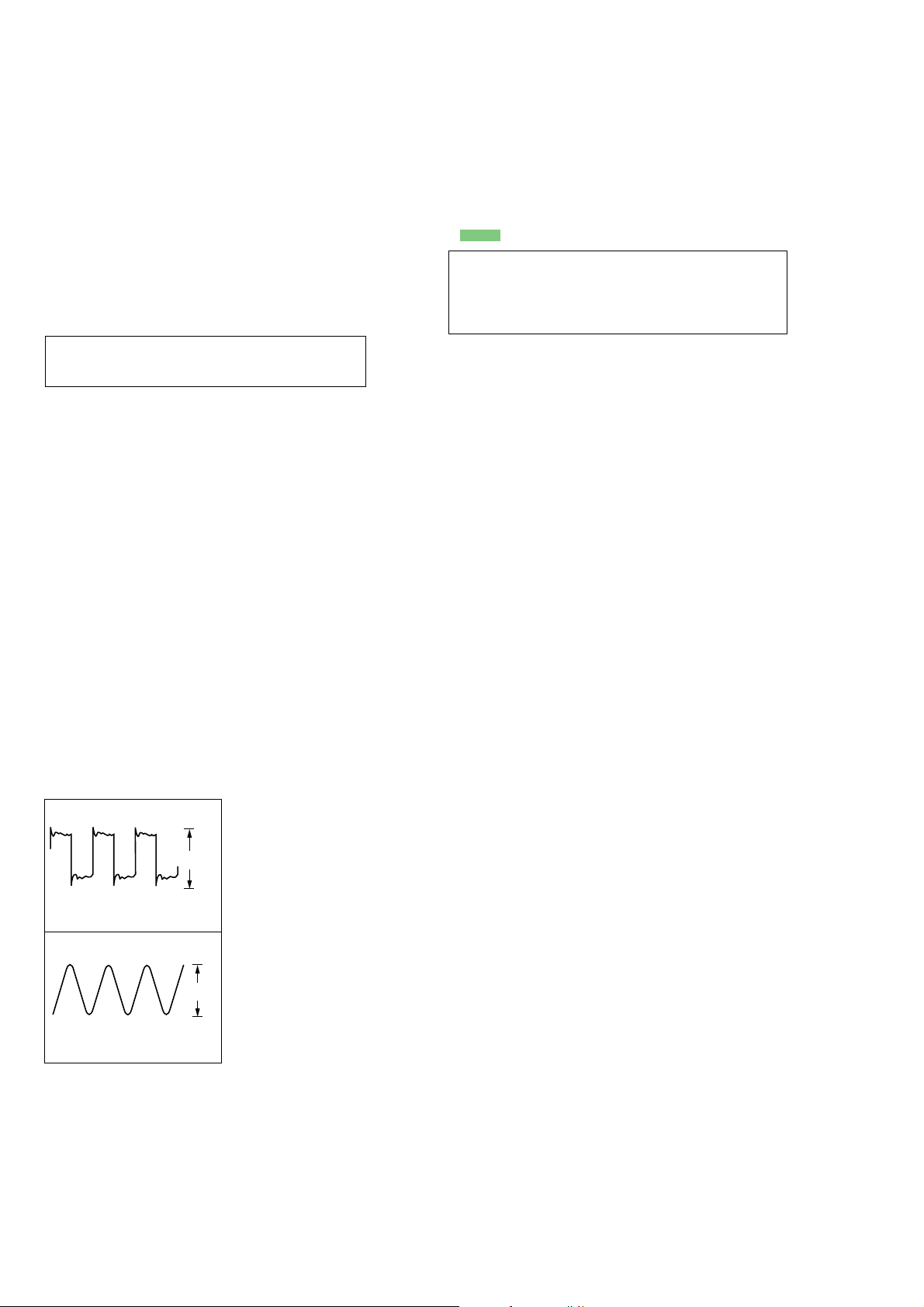
•Waveforms
– MAIN Board –
1 IC300 wl SCKO
1.8432 MHz
2 IC300 is XO
16 MHz
4.5 Vp-p
2V AC/DIV
0.2
µ
sec/DIV
1 Vp-p
0.5V AC/DIV
50nsec/DIV
8
DAB
MODULE
AUDIO_LEFT_OUT
AUDIO_RIGHT_OUT
Q151,
D101-103
OR GATE
SPDIF
S1_IN
S1_DOUT
DAB_OUT
DAB_IN
AM
AC_STOP
86
EEPROM
IC301
IC401
MUTE
Q200
MUTE
Q250
L
R
J201
ANALOG
OUT
DAB
DIGITAL
OPTICAL OUT
59
FL-DATA
53
IC300
SYSTEM CONTROL
52
43
75
74
DAB_IO1
28
DAB_IO2
27
DAB_OUT
DAB_IN
FLASH1
AC_STOP
X_L_MUTING
85
RSTX
77
SDA
34
X0
82
X1
83
SCL
33
X301
16MHz
5
6
54
SIRCS
60
FL CLK
63
FL-CS1
62
FL-CS0
61
FL RST
IC800
FL DRIVER
DA
63
CP
62
CS
61
RESET
60
4
AD1
3
AD2
P36-70
P1-35
5
39
40
55
SEG1
SEG35
COM1
COM16
FLUORESCENT
INDICATOR
TUBE
NC
FL800
IC801
FL DRIVER
DA
63
CP
62
CS
61
RESET
60
4
AD1
3
AD2
539SEG1
SEG35
FF1
FF2
SIRCS
IC802
1
38
KEY_AD0
39
KEY_AD1
55
KEY3
FUNCTION
KEY
ROTARY
ENCORDER
RV801
S831-833
D201
AC
IN
S901
POWER
-30V REG
Q912
IC907
+5V
REG
5
4
FL -30V
D922-924
Q909
5
4
AC DETECT
IC912
D918
AU -6V
RECT
D901-904
IC901
+10V
REG
1
3
D919
FM+3.3V
D+3.3V
IC903
-6V
REG
2
3
RECT
D911
T901
AU +6V
FM +10V
T902
MUTE +3.3V
POWER
CONTROL
Q910,911
30
DAB_PWR
48
AC_STOP
: DIGITAL OUT
: FM
• Signal path
: ANALOG OUT
GATE
IC403
P36
P71
P72
G1-16
66
JOG_P
67
JOG_M
S841-843
RECT
D914-916
Q910
FMAM +3.3V
DAB +5V
POWER
CONTROL
Q906,908
31
DAB_PWR5
IC910
+3.3V
REG
2
3
D913
IC911
+3.3V
REG
1
2
1
Q202
BUFFER
IC200
Q201
4
DABSEL
4
12
13
3
5
11
9
LPF
IC202
AMP
IC203
FM
COAXIAL
75Ω
FM/AM
TUNER
ANTENA
LCH
RCH
CE
TUNED
STEREO
MUTING
FM_S-METER
RDS_INT
RDS_DATA
SLATCH
TUNED
STEREO
TU_MUTING
S-METER
RDS_INT
RDS_DATA
DAB
COAXIAL
75Ω
ANTENA
CL
DO
DI
TUN_CLK
TUN_DIO2
TUN_DIO1
73
78
14
76
15
SLATCH
TUNED
STEREO
TU_MUTING
S-METER
RDS_INT
RDS_DATA
TUN_CLK
TUN_DIO2
TUN_DIO1
SLATCH
TUNED
STEREO
TU_MUTING
FM_SIG_OUT
RDS_INT
RDS_DATA
TUN_CLK
TUN_DIO2
TUN_DIO1
D +3.3V
IC100
RESET
2
1
1
2
3
6
7
8
FLASH2
RESET
MD0
MD2
51
49
MD0
MD2
FLASH2
FLASH1
FLASH1
FLASH2
WP
32
7
SDA
SCL
WP
X1
83
X302
1.8432MHz
2
POWER
TRNSFORMER
IC902
+6V
REG
1
3
14
IC201
SELECTOR
DIGITAL
TRNSMITTER
CN306
FLASH
PROGRAM
TUNING/
SELECT
REMOTE
SENSOR
D930
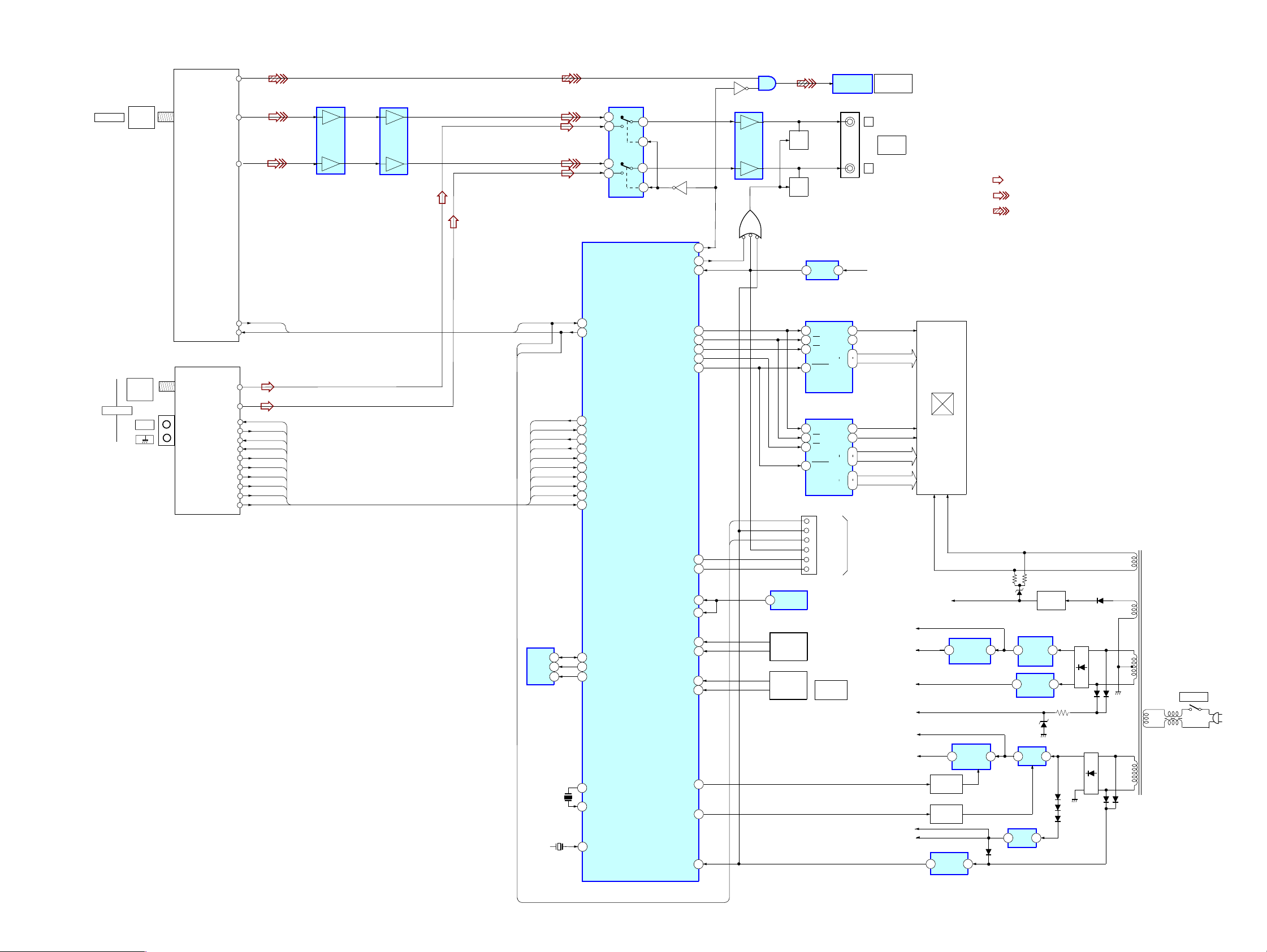
3-1. BLOCK DIAGRAM
ST-SDB900
ST-SDB900
99
 Loading...