

Sony STR-KS1000 Service Manual
STR-KS1000
Q
Q
3
7
6
3
1
5
1
5
0
SERVICE MANUAL
Ver. 1.2 2006.08
TEL 13942296513 QQ 376315150 892498299
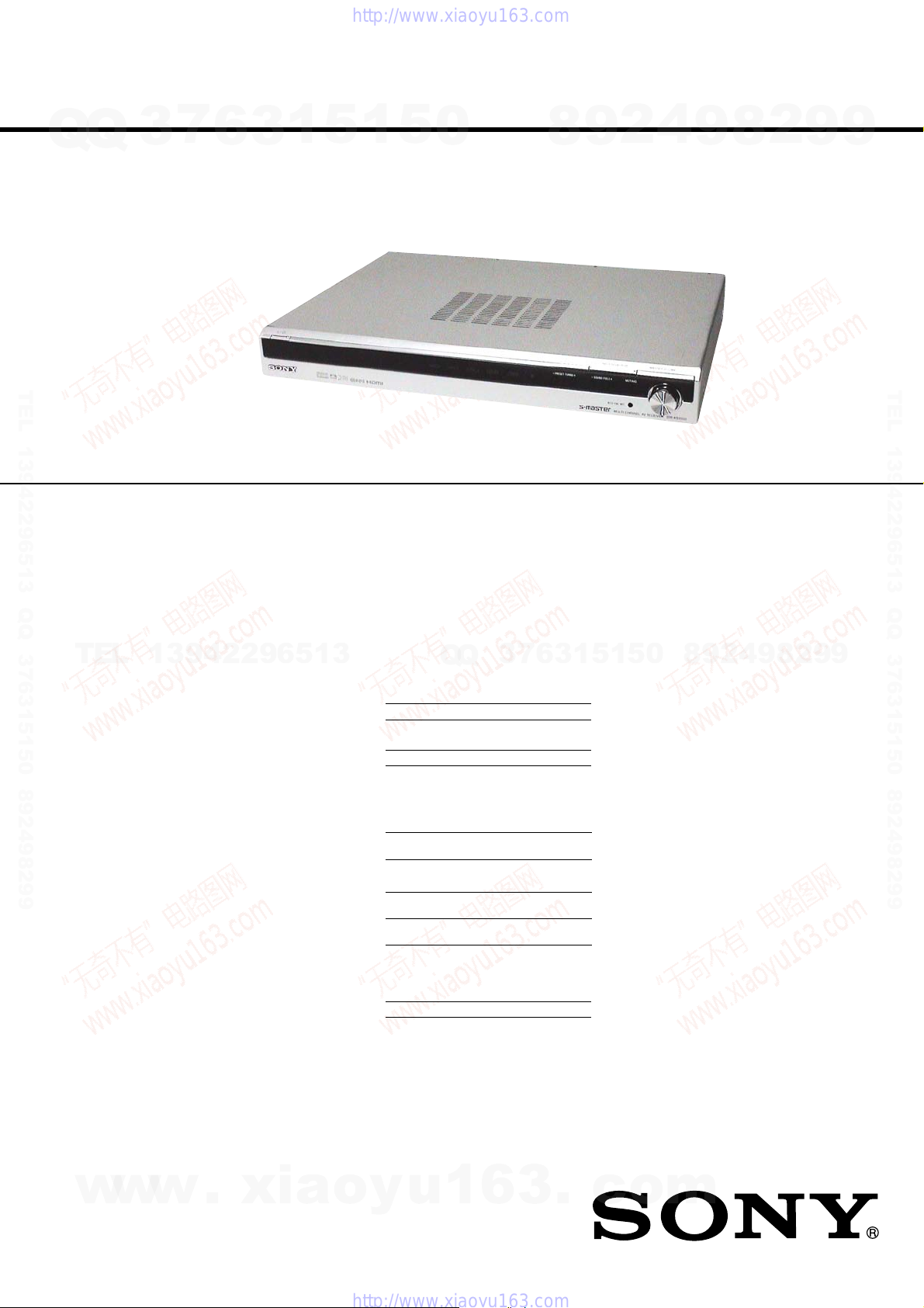
• STR-KS1000 is the receiver section in HT-SF1000/SS1000.
This receiver incorporates Dolby* Digital and Pro
Logic Surround and the DTS ** D igital Surround
System.
*Manufactured under license from Dolby
Laboratories.
“Dolby”, “Pro Logic” and the double-D symbol
are trademarks of Dolb y Laboratories.
**“DTS” and “DTS Digital Surround” are
registered trademarks of Digital Theater
Systems, Inc.
This receiver incorporates High-Definition
Multimedia Interface (HDMI
HDMI, the HDMI logo and High-Definition
Multimedia Interface are trademarks or registered
trademarks of HDMI Licensing LLC.
TM
) technology.
8
9
2
4
9
2
8
9
AEP Model
UK Model
E Model
9
TEL 13942296513 QQ 376315150 892498299
TEL
13942296513
Amplifier section
HT-SF1000 only
Power Output
Stereo mode (rated) 70 W + 70 W
Music power output (reference)
HT-SS1000 only
Power Output
Stereo mode (rated) 70 W + 70 W
Music power output (reference)
1)
(4 ohms at 1 kHz, 0.7%)
FRONT
(With SS-FSP1000)
CENTER
(With SS-CNP1000F)
2)
SUR
(With SS-FRP1000)
SUBWOOFER
(With SS-WP1000)
1)
(4 ohms at 1 kHz, 0.7%)
FRONT
(With SS-MSP1000)
CENTER
(With SS-CNP1000)
2)
SUR
(With SS-SRP1000)
SUBWOOFER
(With SS-WP1000)
2)
: 143 W/ch
2)
: 143 W
: 143 W/ch
2)
: 143 W/ch
2)
: 143 W
: 143 W/ch
2)
: 28
2)
: 285 W
5 W
3
6
7
3
Q
Q
SPECIFICATIONS
1)
Measured under the following conditions:
Area code Power requirements
CEL, CEK, SP, MY,AR230 V AC, 50 Hz
E51
2)
Depending on the sound field settings and the
source, there may be no sound output.
Inputs (Analog)
SA-CD/CD,
VIDEO 1, 2
Inputs (Digit al)
DVD (Coaxial) Sensitivity: −
VIDEO 2, SA-CD/
CD (Optical)
Reproduction frequency range:
Tone
Gain levels ±6 dB, 1 dB step
240 V AC, 50 Hz
Sensitivity: 1 V
Impedance: 50 kohms
Impedance: 75 ohms
Sensitivity: −
Impedance: −
28 − 20,000 Hz
1
5
4
2
9
8
0
5
1
FM tuner section
Tuning range 87.5 - 108.0 MHz
Antenna FM wire antenna
Antenna terminals 75 ohms, unbalance d
Intermediate frequency
AM tuner section
Tuning range
Models of area code CEL, CEK SP, MY,
With 9-kHz tuning scale:
Models of area code E51
With 10-kHz tuning scale:
With 9-kHz tuning scale:
Models of area code AR
With 10-kHz tuning scale:
Antenna Loop antenna
Intermediate frequency
3)
You can c h a nge the AM tuning scale to 9 kH z or
10 kHz. After tuning in any AM station, turn off
the receiver. While holding down PRESET
TUNING +, press ?/1. All preset stations will be
erased when you change the tuning scale. To reset
the scale to 10 kHz (or 9 kHz), repeat the
procedure.
10.7 MHz
531 − 1,602 kHz
530 − 1,610 kHz
531 − 1,602 kHz
530 − 1,610 kHz
450 kHz
– Continued on next page –
9
8
2
9
9
3)
3)
w
w
9-887-058-03
2006H05-1
© 2006.08
w
.
xia
Sony Corporation
Home Audio Division
Published by Sony Techno Create Corporation
o
y
u
1
6
MULTI CHANNEL AV RECEIVER
3
.
c
o
m

STR-KS1000
T
Ver. 1.2
General
Power requirements
Q
Q
Area code Power requirements
CEL, CEK 230 V AC, 50/60 Hz
AR
E51 120 − 240 V AC,
SP, MY 230 − 240 V AC,
Power consumption
Po
wer consumption (during standby mode)
Dimensions (w/h/d) (Approx.)
Mass (Approx.) 3.5 kg
TEL 13942296513 QQ 376315150 892498299
Design and specifications are subject to change
without notice.
• Abbreviation
AR : Argentina model
E51 : Chilean and Peruvian models
MY : Malaysia model
SP : Singapore model
About area codes
The area code of the receiver you purchased is
shown on the lower portion of the rear p anel (see
the illustration below).
OR OUT
TEL
– +
– + – + – + – + – +
FRONT R
FRONT L
SUR R SUR L CENTER
Any differences in operation, acco rding to t he area
code, are clear ly indi cated i n the te xt, fo r exam ple,
“Models of area code AA only”.
Notes on chip component replacement
• Never reuse a disconnected chip component.
• Notice that the minus side of a tantalum capacitor may be
damaged by heat.
7
3
220 − 230 V AC,
50/60 Hz
50/60 Hz
50/60 Hz
110 W
0.3 W
430 × 64 × 338 mm
including project i ng parts
and controls
13942296513
SUBWOOFER
6
3
Area code
1
5
1
5
0
1. SERVICING NOTES ............................................... 3
2. GENERAL ................................................................... 4
3. DISASSEMBLY
3-1. Disassembly Flow ........................................................... 6
3-2. Case (SL06)..................................................................... 6
3-3. Front Panel Assy.............................................................. 7
3-4. HDMI Board
(Except Chilean, Peruvian and Argentina models).......... 7
3-5. MAIN Board.................................................................... 8
4. TEST MODE.............................................................. 9
5. DIAGRAMS
5-1. Block Diagram – MAIN Section –................................. 11
5-2. Block Diagram – AMP Section – ................................... 12
5-3. Block Diagram – HDMI Section
(Except Chilean, Peruvian and Argentina models) –....... 13
5-4. Block Diagram
– PANEL, POWER SUPPLY Section – .......................... 14
5-5. Printed Wiring Board – IO Board –................................ 16
5-6. Printed Wiring Board – ADCC Board –......................... 17
5-7. Schematic Diagram – IO Section – ................................ 18
5-8. Printed Wiring Board
– MAIN Board (Component Side) – ............................... 20
5-9. Printed Wiring Board
– MAIN Board (Conductor Side) – ................................. 21
5-10. Printed Wiring Board – SPEAKER Board – .................. 22
5-11. Schematic Diagram – MAIN Section (1/7) – ................. 23
Q
Q
5-12. Schematic Diagram – MAIN Section (2/7) – ................. 24
5-13. Schematic Diagram – MAIN Section (3/7) – ................. 25
5-14. Schematic Diagram – MAIN Section (4/7) – ................. 26
5-15. Schematic Diagram – MAIN Section (5/7) – ................. 27
5-16. Schematic Diagram – MAIN Section (6/7) – ................. 28
5-17. Schematic Diagram – MAIN Section (7/7) – ................. 29
5-18. Printed Wiring Board – HDMI Board
5-19. Schematic Diagram – HDMI Board
5-20. Printed Wiring Boards – DISPLAY Section –................ 32
5-21. Schematic Diagram – DISPLAY Section –.................... 33
7
3
(Except Chilean, Peruvian and Argentina models) –....... 30
(Except Chilean, Peruvian and Argentina models) –....... 31
TABLE OF CONTENTS
4
2
9
8
8
0
5
1
5
1
3
6
9
9
8
2
4
2
9
8
9
2
9
9
TEL 13942296513 QQ 376315150 892498299
9
SAFETY-RELATED COMPONENT WARNING!!
COMPONENTS IDENTIFIED BY MARK 0 OR DOTTED LINE
WITH MARK 0 ON THE SCHEMATIC DIAGRAMS AND IN
THE PARTS LIST ARE CRITICAL TO SAFE OPERATION.
w
w
REPLACE THESE COMPONENTS WITH SONY PARTS WHOSE
PART NUMBERS APPEAR AS SHOWN IN THIS MANUAL OR
IN SUPPLEMENTS PUBLISHED BY SONY.
2
w
.
xia
6. EXPLODED VIEWS
6-1. Overall Section ................................................................ 44
6-2. MAIN Section ................................................................. 45
7. ELECTRICAL PARTS LIST................................ 46
o
y
u
1
6
3
.
c
o
m
SECTION 1
SERVICING NOTES
UNLEADED SOLDER
Q
TEL 13942296513 QQ 376315150 892498299
Boards requiring use of unleaded solder are printed with the lead-
Q
free mark (LF) indicating the solder contains no lead.
(Caution: Some printed circuit boards may not come printed with
Unleaded solder has the following characteristics.
• Unleaded solder melts at a temperature about 40 °C higher
• Strong viscosity
• Usable with ordinary solder
7
3
the lead free mark due to their particular size)
: LEAD FREE MARK
than ordinary solder.
Ordinary soldering irons can be used but the iron tip has to be
applied to the solder joint for a slightly longer time.
Soldering irons using a temperature regulator should be set to
about 350 °C.
Caution: The printed pattern (copper foil) may peel away if
Unleaded solder is more viscou-s (sticky, less prone to flow)
than ordinary solder so use caution not to let solder bridges
occur such as on IC pins, etc.
It is best to use only unleaded solder but unleaded solder may
also be added to ordinary solder.
6
the heated tip is applied for too long, so be careful!
3
1
5
1
5
0
8
9
2
4
9
STR-KS1000
2
8
9
9
TEL 13942296513 QQ 376315150 892498299
TEL
13942296513
Q
Q
3
7
6
3
1
5
1
5
0
8
9
2
4
9
8
2
9
9
w
w
w
.
xia
o
y
u
1
6
3
.
c
o
m
3
STR-KS1000
q;9 8 7
89q;qaq
q
q
4 3
Ver. 1.2
SECTION 2
GENERAL
This section is extracted from
instruction manual.
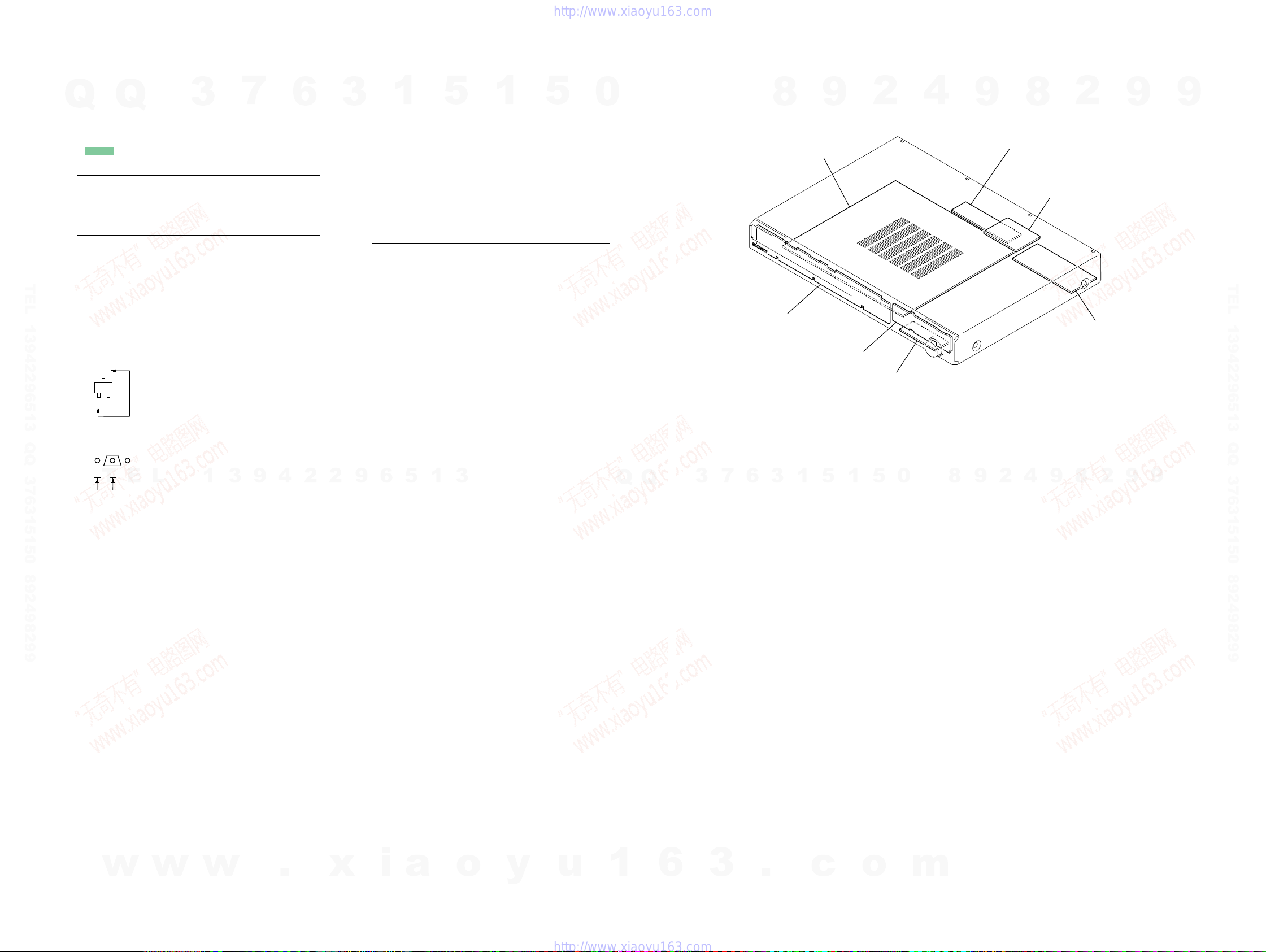
LOCATION OF CONTROLS
Q
Q
Getting Started
3
7
6
3
1
5
1
5
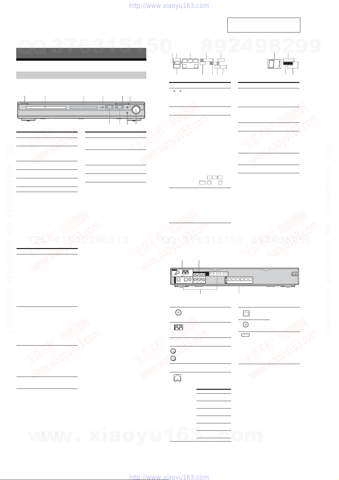
Description and location of parts
Receiver
Front panel
1 52 4 63
MASTER VOLUME
?/1
Name Function
A ?/1 Press to turn the receiver
TEL 13942296513 QQ 376315150 892498299
B Display The current status of the
C Input lamps The lamp of the chosen
D Remote sensor Receives signals from
E INPUT
SELECTOR
F MUTING Press to mute the sound.
on or off.
selected component or a
list of selectable items
appears here.
input source lights up.
remote commander.
Press to select the input
source to playback.
VIDEO 1 VIDEO 2 DVD
SA-CD/CD
TUNER
Name Function
G MASTER
VOLUME
H AUTO CAL MIC
jack
I SOUND FIELD
+/–
J PRESET TUNING
+/–
INPUT SELECTOR
PRESET TUNING SOUND FIELD MUTING
AUTO CAL MIC
Turn to adjust the volume
level of all speaker s at the
same time.
Connects to the supplied
ECM-AC2 optimizer
microphone for the Auto
Calibration function.
Press to select a sound,
field.
Press to select a preset
station.
About the indicators on the display
21 3 4 5 6 7
0
SLEEP
L
CR
LFE
SL SR
SW
S
f
Name Function
A Lights up when the disc being
LFE
played back contains an LFE
(Low Frequency Effect) channel
and the LFE channel signal is
B SLEEP Lights up when the sleep timer is
C Playback
channel
indicators
L
R
C
SL
SR
S
D ;DIGITAL Lights up when Dolby Digital
actually being reproduced.
activated.
The letters (L, C, R, etc.) indicate
the channels being played back.
The boxes around the letters vary
to show how the receiver
downmixes the source sound.
Front Left
Front Right
Center (monaural)
Surround Left
Surround Right
Surround (monaural or the
surround components obtained
by Pro Logic processing)
Example:
Recording format (Front/
Surround): 3/2.1
Sound Field: A.F.D. AUTO
signals are input.
Note
When playing a Dolby Digital
format disc, be sure that you have
made digital connections and the
audio input mode for VIDEO 2
input or SA-CD/CD input is not
set to “V2 ANLG” or “CD
ANLG”.
8
DIGITAL
DTS
d
L
SW
SL SR
9
HDMI
PL
OPT
s
CR
COAX
4
2
Name Function
E HDMI
(Except for
models of
Chilean and
Peruvian)
F Preset
station
indicators
G D.RANGE Lights up when dynamic range
H Tuner
indicators
I MEMORY Lights up when a memory
J COAX Lights up when the DVD input is
8
9
Lights up when a playback
component is connected to this
receiver using a HDMI jack.
Lights up when using the
receiver to tune in radio stations
you have preset. For details on
presetting radio stations.
compression is activated.
Lights up when using the
receiver to tune in radio stations,
etc.
No
“RDS” lights up for models of
area code CEL, CEK only.
function, such as Preset Memory,
etc., is activated.
selected.
2
D.RANGE
MEMORY
ST MONO
9
RDS
9
TEL 13942296513 QQ 376315150 892498299
TEL
Name Function
K OPT Lights up when
L ;PL(II) Lights up when the receiver
M DTS Lights up when DTS signals are
N SW Lights up when the audio signal
w
13942296513
–audio input mode for VIDEO 2
input is set to “V2 AUTO” and
the source signal is a digital
signal being input through
VIDEO 2 OPT IN jack.
–audio input mode for SA-CD/
CD input is set to “CD AUTO”
and the source signal is a
digital signal being input
through SA-CD/CD OPT IN
jack.
–audio input mode for VIDEO 2
input or SA-CD/CD input is set
to “V2 OPT” or “CD OPT”.
applies Pro Logic processing to 2
channel signals in order to output
the center and surround channel
signals. “; PLII” lights up
when the Pro Logic II Movie/
Music decoder is activated.
Note
Dolby Pro Logic and Dolby Pro
Logic II decoding do not
function for DTS format signals.
input.
Note
When playing a DTS format
disc, be sure t ha t y o u have made
digital connections and the audio
input mode for VIDEO 2 input
or SA-CD/CD input is not set to
“V2 ANLG” or “CD ANLG”.
is output from the
SUBWOOFER jack.
w
w
.
xia
o
y
u
3
Q
Q
Rear panel
1 2
ANTENNA
AM
U
OPT IN
OPT IN
DIGITAL
SA-CD/CD
VIDEO 2
A ANTENNA section
B AUDIO INPUT section
White (L)
Red (R)
C SPEAKER section
1
6
3
6
7
SA-CD/CD
VIDEO 2
VIDEO 1
LRL
HDMI
R
COAX IN
AUDIO IN
AUDIO IN
AUDIO IN
DVD
FM
ANTENNA
AM
ANTENNA
AUDIO IN
jack
Connects to speakers.
The following table shows
the respective color for the
speaker jacks.
Speaker jack Color
FRONT R
(Front right speaker)
FRONT L
(Front left speaker)
SUR R
(Surround right speaker)
SUR L
(Surround left speaker)
CENTER
(Center speaker)
SUBWOOFER
(Sub woofer)
3
.
1
5
1
DVD IN VIDEO 2 IN MONITOR OUT
Connects to the
FM wire antenna
supplied with this
receiver.
Connects to the
AM loop antenna
supplied with this
receiver.
Connects to a
satellite tuner, CD
player, etc.
Red
White
Grey
Blue
Green
Purple
c
2
9
8
0
5
– +
– + – + – + – + – +
FRONT R
FRONT L
SUR R SUR L CENTER
SUBWOOFER
D DIGITAL INPUT/OUTPUT section
OPTICAL
IN jack
COAXIAL
IN jack
HDMI IN/
MONITOR
OUT jack
(Except for
models of
Chilean,
Peruvian
and
Argentina)
o
m
2
8
9
4
Connects to a DVD
player, etc. The COAX
IN jack provides a better
quality of loud sound.
Connects to a DVD
player or a satellite tuner.
An image and the sound
are output to a TV or a
projector.
9
9
4
F DUAL MONO Press to select the language
you want during digital
broadcast.
G FM MODE Press to select FM monaural
or stereo reception.
H D.TUNING Press to enter direc t tuni ng
mode.
D.SKIP Press to skip disc of the CD
player or DVD player (multidisc changer only).
I ENTER Press to enter the value after
selecting a channel, disc or
track using the numeric
buttons.
MEMORY Press to store a station.
J DVD MENU Press to display the menu of
the DVD player on the TV
screen. Then, use the control
buttons to perform menu
operations.
K TOOLS Press to display options
applicable to the enti re disc
(e.g. disc protection), recorder
(e.g. audio settings during
recording), or multiple items
on a list menu (e.g. erasing
multiple titles).
L MUTING Press to mute th e sound.
M TV VOL
+
a)
/–
Press TV VOL +/– and TV
(P) at the same time to adjust
the TV volume level.
MASTER
VOL +
a)
/–
Press to adjust the volume
level of all speakers at the
same time.
N MENU Press to display the menus of
the VCR, DVD player, or
satellite tuner on the TV
screen. Then, use the control
buttons to perform menu
operations.
Name Function Name Function
O ./> Press to skip tracks of the CD
player, DVD player, MD
deck, or tape deck.
REPLAY /
ADVANCE
Press to replay the previous
scene or fast forward the
current scene of the VCR or
DVD player.
m/M Press to
–search tracks in the forward/
backward direction of the
DVD player.
–fast forward/rewind of the
VCR, CD player, MD deck,
or tape deck.
H
a)
Press to start playback of the
VCR, CD player, DVD player ,
MD deck, or tape deck.
X Press to pause playback or
recording of the VCR, CD
player, DVD player, MD
deck, or tape deck. (Also
starts recording with
components in recording
standby.)
x Press to stop playback of the
VCR, CD player, DVD player ,
MD deck, or tape deck.
TV CH +/– Press TV CH +/– and TV (P)
at the same time to select
preset TV channels.
PRESET +/– Press to select
–preset stations.
–preset channels of the VCR
or satellite tuner.
TUNING +/– Press to scan a station.
P TV To ac tivate t he buttons with
orange printing, press TV and
the button with orange
printing simultaneously.
Q RETURN/
EXIT O
Press to
–return to the previous menu.
–exit the menu while the
menu or on-screen guide of
the VCR, DVD player, or
satellite tuner is displayed
on the TV screen.
<
<
STR-KS1000
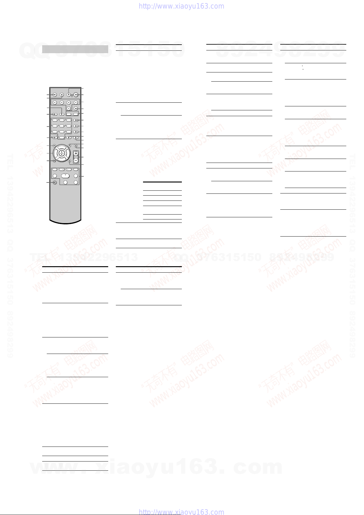
Remote commander
Q
TEL 13942296513 QQ 376315150 892498299
You can operate the receiver with the supplied
Q
remote. You can also use the remote to control
the Sony audio/video components that the
remote is assigned to operate.
RM-AAU006
wg
wf
wd
ws
wa
w;
ql
qk
qj
RETURN/EXIT
qh
7
3
TV/VIDEO
SLEEP
VIDEO 1 VIDEO 2 DVD SA-CD/CD
2CH A.F.D.
123
46
78
>10/
-
CLEAR
Gg
TV CH –
PRESET –
.
TUNING –
TV
TV
AUTO
AV
CAL
?/1
SYSTEM STANDBY
TUNER
AMP MENU
MOVIE MUSIC
DUAL MONO
FM MODE
5
D.TUNING
9
D.SKIP
MEMORY DVD MENU
0/10
ENTER
MUTING
TOOLSDISPLAY
F
TV VOL
MASTER VOL
f
MENU
TV CH +
REPLAY ADVANCE
PRESET +
<
<
TUNING +
HmM
Xx
?/1
?/1
>
6
AV ?/1
1
(on/standby) switch
TV ?/1, ?/1
2
(
on/standby) switch
3
4
5
6
7
8
9
q;
qa
qs
qd
qf
qg
3
Name Function
A AV ?/1 Press to turn on or off the
1
5
1
5
Sony audio/video components
that the remote is assigned to
operate.
If you press ?/1 (B) at the
same time, it will turn off the
receiver and other
components (SYSTEM
STANDBY).
Note
The function of the AV ?/1
switch changes automatically
each time you press the input
B TV ?/1 Press TV ?/1 and TV (P) at
?/1 Press to turn the receive r on or
C Input buttons Press one of the buttons to
D AMP MENU Press to display the menu of
E MOVIE,
MUSIC
buttons (C).
the same time to t u r n the TV
on or off.
off.
To t urn off all components,
press ?/1 and A V ?/1 (A) at
the same time (SYSTEM
STANDBY).
select the component you
want to use. When you press
any of the input buttons, the
receiver turns on. The buttons
are factory assigned to control
Sony components as follows.
You can change the button
assignments following the
steps in “Changing button
assignments”.
Button Assigned Sony
component
VIDEO 1 VCR (VTR mode 3)
VIDEO 2 VCR (VTR mode 2)
DVDDVD player
SA-CD/CD Super Audio CD/CD
player
TUNER Built-in tuner
the receiver. Then, use the
control buttons to perform
menu operations.
Press to select sound fields for
movie or music.
0
8
9
2
4
9
8
2
9
9
TEL 13942296513 QQ 376315150 892498299
TEL
w
13942296513
Name Function
R Control
buttons
S DISPLAY Press to
T -/-- Press -/-- and TV (P ) at the
>10/
CLEAR Press to
U Numeric
buttons
(number 5
V 2CH Press to select 2CH STEREO
W A.F.D. Press to select A.F.D. mode.
X AUTO CAL Press to activate the Auto
w
After pressing AMP MENU
(D), DVD MENU (J), or
MENU (N), press the control
button V, v, B or b to select
the settings. When you press
DVD MENU or MENU, press
the control button to enter the
selection.
–s el ect i nformation displayed
–select information displayed
same time to select the
channel entry mode, either
one or two digits of the TV.
x
Press to select
–track numbers over 10 of the
–channel numbers of the
–clear a mistake when you
–return to continuous
Press to
–preset/tune to preset
a)
)
–select track numbers of the
–select channel numbers of
Press the numeric buttons and
TV (P) at the same time to
select the TV cha nnels.
mode.
Calibration function.
w
on the receiver’s display (for
TUNER input only).
on the TV screen of the
VCR, satellite tuner, CD
player, DVD player, or MD
deck.
VCR, satellite tuner, CD
player or MD deck.
Digital CATV terminal.
press the incorrect numeric
button.
playback, etc. of the satellite
tuner or DVD player.
stations.
CD player, DVD player or
MD deck. Press 0/10 to
select track number 10.
the VCR or satellite tuner.
b)
.
xia
Q
Name Function
Y TV/VIDEO Pre ss TV/VIDEO and TV
SLEEP Press to activate the Sleep
a)
The number 5, MASTER VOL +, TV V O L +, and
H buttons have tactile dots. Use the tactile dots as
references when operating th e receiver.
b)
Models of area code CEL, CEK only.
Notes
Some functions explained in this section may not
work depending on the model.
The above explanation is intended to serve as an
example only. Therefore, depending on the
component, the above operation may not be
possible or may operate dif ferently than described.
(P) at the same time to select
the input signal (TV input or
video input).
Timer function and the
duration which the receiver
turns off automatically.
o
y
u
1
Q
3
6
6
7
3
3
.
1
1
5
c
0
5
o
9
8
m
2
4
9
8
2
9
9
5
s
STR-KS1000
• This set can be disassembled in the order shown below.
7
Q
Q
3-1. DISASSEMBLY FLOW
3
SET
3-2. CASE (SL06)
(Page 6)
6
3
1
5
SECTION 3
DISASSEMBLY
1
5
0
8
9
2
4
9
8
2
9
9
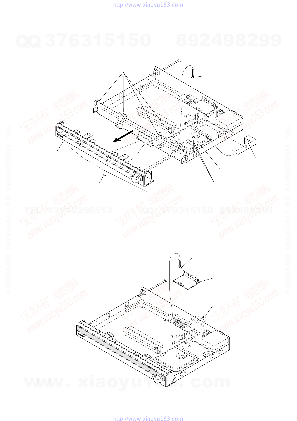
3-3. FRONT PANEL ASSY
(Page 7)
TEL 13942296513 QQ 376315150 892498299
Note: Follow the disassembly procedure in the numerical order given.
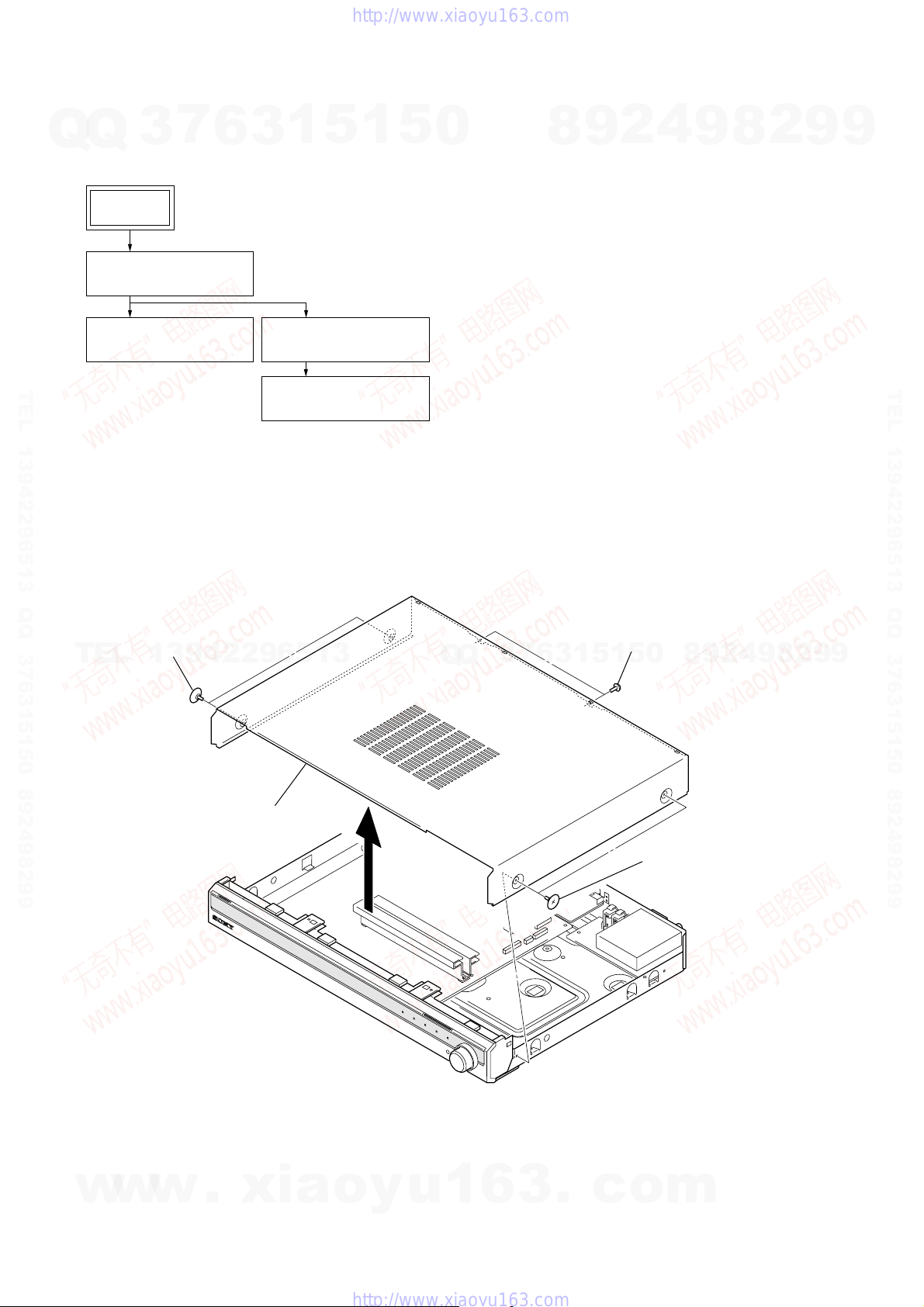
3-2. CASE (SL06)
2
TEL
two tapping screws
13942296513
3-4. HDMI BOARD
(Page 7)
3-5. MAIN BOARD
(Page 8)
Q
Q
3
7
6
3
1
5
1
1
two screws
(BVTP3 × 8)
0
5
8
9
2
4
9
8
2
9
TEL 13942296513 QQ 376315150 892498299
9
w
w
w
3
case (SL06)
.
xia
o
y
u
1
6
3
.
c
2
two tapping screw
o
m
6
3
screw
(BVTP3
×
6)
5
four screws
(BVTP3
×
6)
7
front panel assy
4
two harnesses
6
four claws
1
wire (flat type) (17 core)
(CNS193)
2
connector
(CNP196)
d
Q
3-3. FRONT PANEL ASSY
7
Q
3
6
3
1
5
1
5
0
8
9
2
4
9
STR-KS1000
2
8
9
9
TEL 13942296513 QQ 376315150 892498299
TEL
13942296513
3-4. HDMI BOARD
(Except Chilean, Peruvian and Argentina models)
Q
Q
3
7
6
3
1
1
5
1
connector
(CN5004)
5
0
8
9
2
4
9
8
2
9
TEL 13942296513 QQ 376315150 892498299
9
w
w
w
3
HDMI boar
.
xia
o
y
u
1
6
3
.
c
2
three screws
×
6)
(B3
o
m
7
STR-KS1000
Ver. 1.2
3-5. MAIN BOARD
7
Q
Q
TEL 13942296513 QQ 376315150 892498299
qa
3
qd
two radiation sheets (AMP)
6
connector
(CN901)
six screws
(BVTP3
×
6)
6
9
heat sink (AMP)
3
1
5
7
1
screw
(BVTP3
5
×
12)
8
two screws
(BVTP3
0
×
8)
0
three screws
(BVTP3
×
6)
4
2
9
8
5
connector (CNP196)
2
wire (flat type) (15 core) (AEP, UK)
wire (flat type) (11 core) (Singapore,
Malaysia, Chilean, Peruvian and
Argentina models) (CNS195)
3
9
wire (flat type) (13 core)
(CNS198)
8
2
9
9
TEL 13942296513 QQ 376315150 892498299
qs
MAIN board
TEL
13942296513
Q
Q
3
6
7
3
1
two connector
(CNP500, CNP510)
1
5
8
0
5
1
4
wire (flat type) (17 core)
(CNS193)
9
2
4
9
8
2
9
9
8
w
w
w
.
xia
o
y
u
1
6
3
.
c
o
m
SECTION 4
TEST MODE
STR-KS1000
FACTORY PRESET MODE
Q
TEL 13942296513 QQ 376315150 892498299
All preset contents are reset to the default setting.
Q
Procedure:
1. While pressing the [SOUND FIELD --] and [PRESET TUNING
2. The message “FACTORY” appears and the present contents
ALL CLEAR MODE
All preset contents are cleared when this mode is activated. Use
this mode before returning the product to clients upon completion
of repair.
Procedure:
1. While pressing the [INPUT SELECTOR] and [PRESET TUNING
2. The message “CLEARED” appears.
FL CHECK MODE
All fluorescent segments are tested. When this test is activated, all
segments turn on at the same time, then each segment turns on one
after another.
Procedure:
1. While pressing the [MUTING] and [PRESET TUNING --] buttons,
2. All segments and all LEDs turn on.
3. Press the [INPUT SELECTOR] button.
4. Half of segments and [VIDEO 1], [SA-CD/CD] LEDs turn on.
5. Press the [INPUT SELECTOR] button once again.
6. Others half of segments and [VIDEO 2], [DVD] LEDs turn on.
7. Press the [INPUT SELECTOR] button once again.
8. All segments and all LEDs turn off.
TEL
VERSION MODE
When this mode is used, the model, the destination and the software
version number are displayed.
Procedure:
1. While pressing the [SOUND FIELD +] and [PRESET TUNING --]
2. The model, the destination and the software version number
KEY CHECK MODE
This mode is used to check the key.
Procedure:
1. While pressing the [MUTING] and [INPUT SELECTOR] buttons,
2. The message “REST 06” appears.
3. Every pressing of any button other than the I/1 button counts
4. When all buttons are pressed, the message “REST 00” appears.
PROTECTOR AUTO OFF MODE
When this mode is used, a protector on state is maintainable.
Procedure:
1. While pressing the [MUTING] and [SOUND FIELD --] buttons,
2. The message “PROT EVER” appears.
7
3
+] buttons, press the
are reset to the default values.
+] buttons, press the I/1 button to turn on the main power.
press the I/1 button to turn on the main po wer.
6
13942296513
buttons, press the I/1 button to turn on the main power.
appear.
press the I/1 button to turn on the main power.
down the buttons. The b uttons which are already counted once
are not counted again.
press the I/1 button to turn on the main power.
1
5
1
3
I/1 button to turn on the main power .
5
0
Q
Q
SOUND FIELD CLEAR MODE
The preset sound field is cleared when this mode is activated. Use
this mode before returning the product to clients upon completion
of repair.
Procedure:
1. While pressing the [SOUND FIELD +] button, press the I/1
2. The message “SF. CLR.” appears and initialization is
RDS AUTOBETICAL MODE
(AEP AND UK MODELS ONLY)
Procedure:
1. While pressing the [INPUT SELECTOR] button, press the I/1
2. The message “AUTO-BET” appears and scans and stores all
3. When done, the message “FINISH” appears.
VACS OFF MODE
This mode is used to switch off the VACS (Variable Attenuation
Control System).
Procedure:
1. While pressing the [SOUND FIELD --] and [PRESET TUNING --]
2. The message “VACS OFF” appears and the switch off the
TUNER CHECK MODE
Tuner is tested
Procedure:
1. While pressing the [SOUND FIELD +] and [INPUT SELECTOR]
7
3
2. The message “TUN CHK” appears and tuner is tested.
SWAP ALL MODE
When this mode is used, output the audio signal of front L/R channel
to all channel.
Procedure:
1. While pressing the [MUTING] and [PRESET TUNING +] buttons,
2. The message “SWP. ALL” appears .
3. Each time [PRESET TUNING +] or [PRESET TUNING --] button
CHANGE-OVER THE AM TUNING INTERVAL
(CHILEAN AND PERUVIAN MODELS ONLY)
The AM tuning interval can be changed over 9 kHz or 10 kHz.
Procedure:
1. While pressing the [PRESET TUNING +] button, press the I/1 button
2. The AM turning interval changed over 9 kHz or 10 kHz.
4
2
9
8
button to turn on the main power.
performed.
button to turn on the main power.
the FM and FM RDS stations in the broadcast area.
buttons, press the I/1 button to turn on the main power.
VACS .
0
5
1
5
1
3
6
buttons, press the I/1 button to turn on the main power.
press the I/1 button to turn on the main power.
is pressed, output channel is switched.
to turn on the main power.
9
8
9
2
8
4
2
9
8
9
2
9
9
9
TEL 13942296513 QQ 376315150 892498299
w
w
w
.
xia
o
y
u
1
6
3
.
c
o
m
9
STR-KS1000
DCAC FACTORY TEST MODE
Procedure:
Q
Q
1. Press the buttons of standard commander (RM-AAU002) (PART
No. : 1-479-148-11 ) in order of [TUNER] → [JUMP] → [JUMP] →
[JUMP] → [MASTER VOL +] → [DUAL MONO].
2. The following content is displayed on the fluorescent indicator
tube, and DCAC factory test mode is started.
When the error happens, the following content is displayed
on the fluorescent indicator tube.
TEL 13942296513 QQ 376315150 892498299
7
3
DCAC X
ERR SD0X
1
6
3
figure of 1 to 4
1: Abnormality of D1502 or R1100
2: Abnormality of D1501
3: Abnormality of D1500
5
1
5
0
8
9
2
4
9
8
2
9
9
TEL 13942296513 QQ 376315150 892498299
3. Connect front L-ch speaker of receiver and AUTO CAL
microphone.
4. Turn the [MASTER VOLUME] jog, there will be test tone sound
output from front L-ch speaker, and the following content is
displayed on the fluorescent indicator tube.
AD - XXX
figure of 0 to 255
(depends on loudness of test tone)
TEL
13942296513
Q
Q
3
7
6
3
1
5
1
5
0
8
9
2
4
9
8
2
9
9
10
w
w
w
.
xia
o
y
u
1
6
3
.
c
o
m
SECTION 5
DIAGRAMS
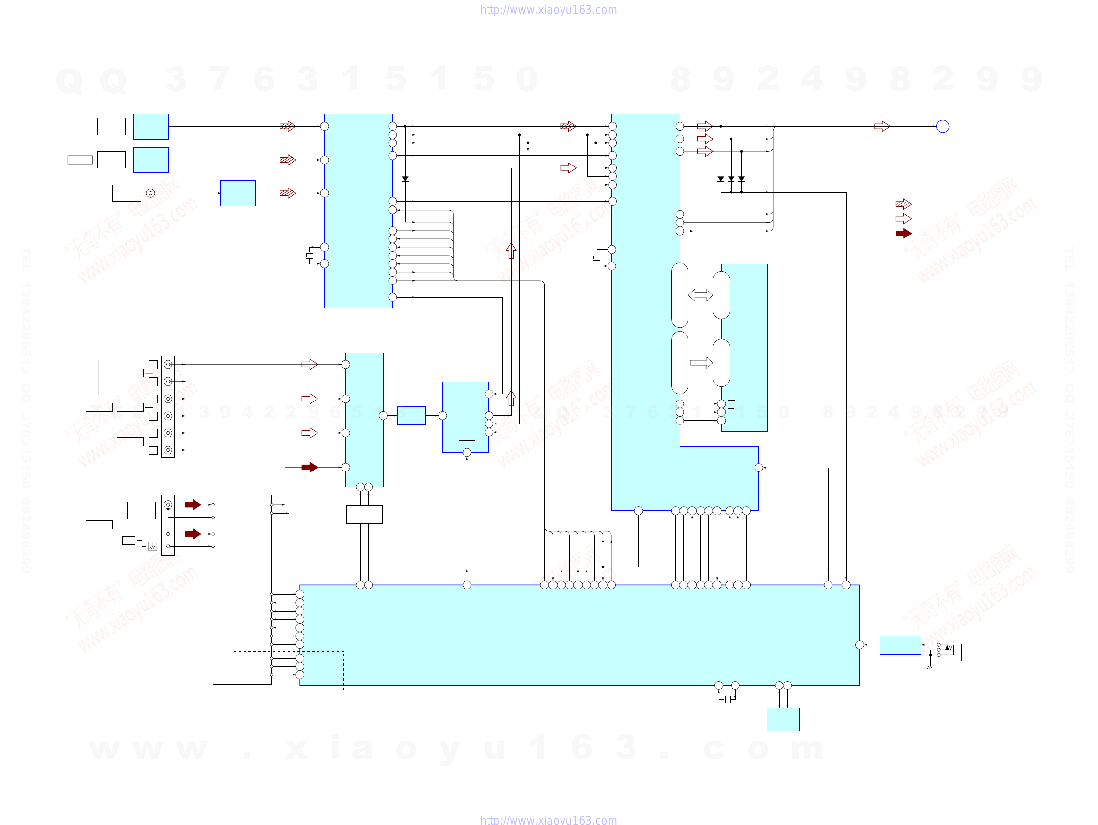
5-1. BLOCK DIAGRAM – MAIN Section –
Q
DIGITAL
Q
OPT IN
SA-CD/CD
OPT IN
VIDEO 2
J1700
COAX IN
DVD
OPTICAL
RECEIVER
IC1700
OPTICAL
RECEIVER
IC1701
3
7
SCHMITT
TRIGGER
IC1702
6
3
TEL 13942296513 QQ 376315150 892498299
X1301
12.288MHz
1
DIGITAL AUDIO
INTERFACE RECEIVER
DIN0
3
DIN1
4
DIN2
5
21
XOUT
22
XIN
IC1301
DATAO
BCK
LRCK
CKOUT
AUDIO
CKSEL1
CLK
XMODE
XSTATE
ERROR
XMCLK
5
DO
DI
CE
STR-KS1000
Ver. 1.2
1
16
14
15
13
D1301
24
47
35
36
38
37
48
17
34
20
DIR CKSEL
DIR DATA0
DIR DO
DIR DI
DIR CLK
DIR CE
DIR XMODE
DIR XSTATE
DIR ERROR
5
0
X1502
13.9MHz
DIGITAL AUDIO
SIGNAL PROCESSOR
IC1501
SDI2
30
BCKI2
29
LRCKI2
28
KFSIO
22
SDI1
18
BCKI1
17
LRCKI1
15
GP8
69
12
MCLK2
9
MCLK1
SDO1
SDO2
SDO3
SCKOUT
BCKO
LRCKO
8
23
24
25
14
20
19
D0 – D15A0 – A15
9
D1502
7 – 10, 13 – 16,
98, 80 – 77, 75 – 72
108, 107, 105 – 102, 99,
29 – 32, 35 – 38
D1501
S-RAM
IC1502
D0 – D15
D1500
2
DATA1
DATA2
DATA3
SCK
BCK
LRCK
4
9
8
DATA1 – DATA3,
SCK, BCK, LRCK
• R-ch is omitted due to same as L-ch.
• SIGNAL PATH
2
A
: DIGITAL INPUT
: ANALOG INPUT
: TUNER
9
(Page 12)
9
TEL 13942296513 QQ 376315150 892498299
J1710
T
ANTENNA
E
SA-CD/CD
VIDEO 2AUDIO IN
L
VIDEO 1
FM 75Ω
COAXIAL
AM
ANALOG AUDIO
X
1
B
21
SELECT_B
SELECT_A
INPUT SELECT
13
3
IC1710
BUFFER
IC1600
A/D CONVERTER
IC1602
LIN
1
PDWN
7
10
SCKI
DOUT
BCK
LRCK
AD_RST
A0 – A15
1
HCLK
HCS
5
HACN
5 – 1, 44 – 42,
27 – 24, 21 – 18
OE
41
CS
6
1
WE
17
113
7 6 9
PM
GP9
X0
X1
82 83
X1101
24MHz
BST
XRST2GP12
37
GP12
XRST
5
56
0
SDA33SCL
34
EEPROM
IC1131
8
9
9
2
8
9
4
2
9
3
55
BST
ADCC_INT
ADCC2
44
MIC AMP
IC2000
J2000
AUTO
CAL MIC
82 – 85, 66 – 64
15
12
11
10
Q
DIR DATA0
1
Q
DIR DI
DIR DO
DIR CLK
98DI97
95CE96
DO
CLK
DATA0
SYSTEM CONTROLLER
DIR CE
DIR XMODE
DIR XSTATE
93
100
XMODE
IC1601 (1/4)
3
DIR CKSEL
DIR ERROR
99
94
ERROR
XSTATE
CKSEL1
7
6
EXLOCK
59
112, 110, 109, 97 – 92,
OE0
43
CS0
44
3
WE0
45
HDOUT35HDIN33HCLK34HCS36HACN32GP968PM
18 19 20 4 5 2
HDIN
HDOUT
X2
6
15
X1
14
5
X0
12
X3
11
10A9
INVERTER
Q1710, 1711
22
L
R
L
R
L
R
1
R-CH
R-CH
R-CH
3
9
4
2
2
TUNER
FM ANT
GND
AM ANT
GND
L CH
R CH
DO/ST
DI
CLOCK
CE
MUTE
TUNED
ST
RDS DATA
RDS_CL
FM SIG OUT RDS SIGNAL
(AEP, UK)
R-CH
88
86
85
87
89
66
90
53
52
43
9
T_DO
T. DATA
T. CLK
SLATCH
T_MUTE
TUNED
ST
RDS DATA
RDS CLK
STR-KS1000
w
w
w
.
x
i
a
o
y
u
1
6
1111
3
.
c
o
m
STR-KS1000
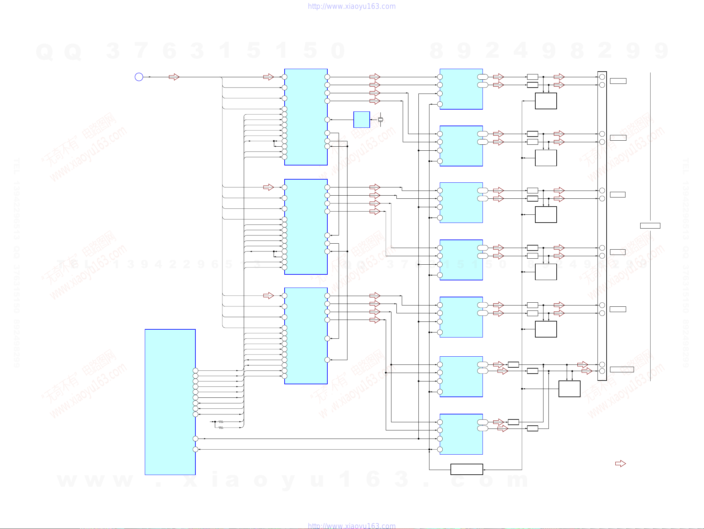
5-2. BLOCK DIAGRAM – AMP Section –
Q
Q
3
(Page 11)
7
A
6
DATA1 – DATA3,
SCK, BCK, LRCK
3
1
TEL 13942296513 QQ 376315150 892498299
T
E
L
1
3
9
4
SYSTEM CONTROLLER
2
IC1601 (2/4)
SOFT_MUTE
POWER_RST
POWER_SD
2
SCDT
SHIFT
LAT1
LAT2
LAT3
INT
OVF
OVFW
9
6
62
61
65
58
69
64
68
78
63
3.3V
32
26
D1
BCK
LRCK
SCK
D2
BCK
LRCK
SCK
5
D3
BCK
LRCK
SCK
SCDT
SHIFT
LAT1
LAT2
LAT3
INIT
OVF
OVF2
SOFT MUTE
PGMUTE
NSP MUTE
1
5
SCDT
SHIFT
LAT1
INIT
NSP MUTE
OVF
SOFT MUTE
PGMUTE
SCDT
SHIFT
LAT2
INIT
NSP MUTE
OVF
SOFT MUTE
PGMUTE
3
SCDT
SHIFT
LAT3
INIT
NSP MUTE
OVF2
OVF
SOFT MUTE
PGMUTE
1
31 DATA
30 BCK
29 LRCK
36 XFSIIN
21 SCDT
22 SCSHIFT
23 SCLATCH
27 INIT
18 NSPMUTE
24 OVF FLAGR
25
19 SOFT MUTE
20 PGMUTE
31 DATA
30 BCK
29 LRCK
36 XFSIIN
21 SCDT
22 SCSHIFT
23 SCLATCH
27 INIT
18 NSPMUTE
24 OVF FLAGR
25
19 SOFT MUTE
20 PGMUTE
31 DATA
30 BCK
29 LRCK
36 XFSIIN
21 SCDT
22 SCSHIFT
23 SCLATCH
27 INIT
18 NSPMUTE
24 OVF FLAGR
25 FLAGL OVF
19 SOFT MUTE
20 PGMUTE
5
STREAM PROCESSOR
IC108
XFSOIN
XFSOOUT 14
FLAGL OVF
STREAM PROCESSOR
FLAGL OVF
FSOCKO
IC109
XFSOIN
XFSOOUT
OUTL1 11
OUTL2 9
OUTR1
OUTR2
FSOI
OUTL1 11
OUTL2
OUTR1
OUTR2
FSOI
0
6
4
48
37
38
9
6
4
48
14
38
Q
STREAM PROCESSOR
IC110
OUTR1 6
4
OUTR2
11
OUTL1
9
OUTL2
48
XFSOIN
FSOI
38
CLOCK
BUFFER
IC305
Q
X450
49.152MHz
3
7
6
8
3
2
17
4
13
2
17
4
13
2
17
4
13
2
17
4
13
2
17
4
13
2
17
4
13
17
4
13
9
DIGITAL POWER AMP
IC102
PWM_BP OUT_B
PWM_AP
/RST
/SD
DIGITAL POWER AMP
PWM_BP OUT_B
PWM_AP
/RST
/SD
DIGITAL POWER AMP
PWM_BP OUT_B
PWM_AP
/RST
/SD
DIGITAL POWER AMP
PWM_BP OUT_B
PWM_AP
/RST
1
/SD
DIGITAL POWER AMP
PWM_BP OUT_B
PWM_AP
/RST
/SD
DIGITAL POWER AMP
PWM_BP OUT_B
PWM_AP
/RST
/SD
DIGITAL POWER AMP
PWM_BP
PWM_AP
/RST
/SD
OUT_A
IC101
OUT_A
IC104
OUT_A
IC103
OUT_A
5
IC105
OUT_A
IC106
OUT_A
IC107
OUT_B2
OUT_A
PROTECT DETECT
Q301
1
29, 30
25, 26
29, 30
25, 26
29, 30
25, 26
29, 30
25, 26
29, 30
25, 26
29, 30
25, 26
29, 30
25, 26
2
5
0
4
L.P.F.
L.P.F.
L.P.F.
L.P.F.
L.P.F.
L.P.F.
L.P.F.
L.P.F.
L.P.F.
L.P.F.
8
L.P.F.
L.P.F.
L.P.F.
L.P.F.
9
OVER LOAD
DETECT
Q103, 104
OVER LOAD
DETECT
Q101, 102
OVER LOAD
DETECT
Q107, 108
9
OVER LOAD
DETECT
Q105, 106
OVER LOAD
DETECT
Q109, 110
2
OVER LOAD
Q111, 112
8
4
DETECT
9
2
TM500
+
_
+
_
+
_
+
_
8
+
_
+
_
9
FRONT L
FRONT R
SURR L
SURR R
9
2
CENTER
SUB WOOFER
• SIGNAL PATH
: AUDIO
9
TEL 13942296513 QQ 376315150 892498299
SPEAKERS
9
STR-KS1000
w
w
w
.
x
i
a
o
y
u
1
6
1212
3
.
c
o
m

5-3. BLOCK DIAGRAM – HDMI Section (Except Chilean, Peruvian and Argentina models) –
Q
CN5001
DVD IN
HDMI
1
3
4
6
7
9
10
12
Q
DATA2+
DATA2–
DATA1+
DATA1–
DATA0+
DATA0–
CLOCK+
CLOCK–
3
7
6
3
HDMI RECIVER, HDMI TRANSCEIVER
77
76
74
73
71
70
68
67
A24
B24
A23
B23
A22
B22
A21
B21
1
IC5001
5
Y4
25
Z4
26
Y3
28
Z3
29
Y2
31
Z2
32
Y1
34
Z1
35
1
5
0
HDMI MONITOR OUT
DATA2+
DATA2–
DATA1+
DATA1–
DATA0+
DATA0–
CLOCK+
CLOCK–
CN5003
1
3
4
6
7
9
10
12
8
9
2
4
9
8
2
STR-KS1000
9
9
Ver. 1.2
SCL (5V)
15
SDA (5V)
16
SCL2
64
SDA2
63
TEL 13942296513 QQ 376315150 892498299
+5V POWER
18
19
CN5002
HDMI
VIDEO IN
1
3
4
6
7
9
10
12
15
16
18
19
HOT PLUG DET
DATA2+
DATA2–
DATA1+
DATA1–
DATA0+
DATA0–
CLOCK+
CLOCK–
T
SCL (5V)
SDA (5V)
+5V POWER
HOT PLUG DET
E
L
1
3
9
4
2
2
HPD2
62
A14
15
B14
14
A13
12
B13
11
A12
9
B12
8
A11
6
B11
5
9
6
SCL1
3
SDA1
2
HPD1
80
SCL_SINK
38
SDA_SINK
39
HPD_SINK
40 19
5
1
3
Q
+5V
REGULATOR
IC5002
SCL (5V)
SDA (5V)
+5V POWER
HOT PLUG DET
Q
15
16
18
3
7
6
3
1
5
1
5
0
8
9
2
4
9
8
2
9
TEL 13942296513 QQ 376315150 892498299
9
STR-KS1000
w
ANALOG SWITCH
w
LEVEL SHIFT
IC5004
IC5005
13
HDMI-DET
w
.
x
S1
21
42
12
14
HDMI-SW1
SYSTEM CONTROLLER
i
a
OEB
HDMI-OEB
IC1601 (3/4)
o
y
1
+5.6V
REGULATOR
IC5006
16
HDMI-CTL
+8VHDMI +3.3V
6
+3.3V
REGULATOR
IC5003
u
1313
3
.
c
• SIGNAL PATH
: HDMI
o
m
STR-KS1000
Ver. 1.2
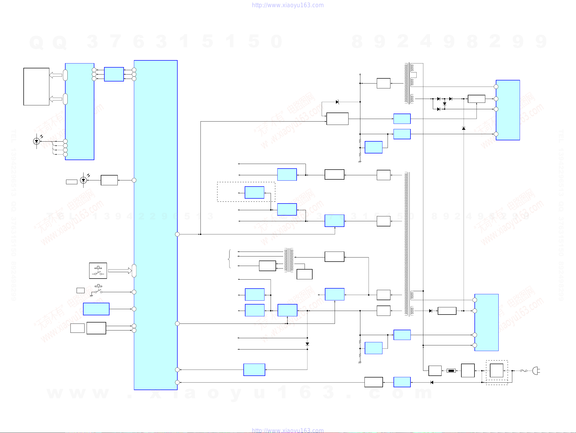
5-4. BLOCK DIAGRAM – PANEL, POWER SUPPLY Section –
Q
Q
INDICATOR TUBE DRIVER,
FLUORESCENT
LED DRIVER
IC700
3
7
6
3
1
5
1
5
0
8
9
2
MAIN POWER
TRANSFORMER
T901
4
9
8
2
9
9
72
73
74
FL_DATA
FL_CLK
FL_STB
FLUORESCENT
INDICATOR TUBE
FL700
14 – 29
SEG1 – SEG16
42 – 31
GRID1 – GRID12
DIN
CLK
STB
7
LEVEL SHIFT
8
9
IC1651
TEL 13942296513 QQ 376315150 892498299
1
DVD LED
2
SA-CD LED
3
E
VIDEO2 LED
4
VIDEO1 LED
D710
TUNER
L
1
LED DRIVE
Q710
3
9
67
4
TUNER_LED
SYSTEM CONTROLLER
IC1601 (4/4)
2
2
9
6
D705 – 708
(PANEL INDICATOR)
T
5
1
3
(AEP, UK)
RDS +3.3V
AMP +12V
A +5V
D +9V
+8V
+3.3V
REGULATOR
IC1711
+5V
REGULATOR
IC1033
+9V
REGULATOR
IC1712
Q
Q
3
D932
POWER ON/OFF
CONTROL
Q943, 947
B+ SWITCH
Q945
+12V
6
7
REGULATOR
IC941
AMP +30.5V
3
SHUNT
REGULATOR
IC931
1
5
RECT
D931
RECT
D944
RECT
D941
1
ISOLATOR
PC903
ISOLATOR
PC901
SUB POWER
TRANSFORMER
T902
5
0
D905
D914, 915
8
9
D908
D906, 907
D910
2
B+ SWITCH
4
Q901
9
POWER CONTROL
3
D
4
VCC
1
OCP/SYNC
5
FB/OLP
8
2
IC901
9
TEL 13942296513 QQ 376315150 892498299
9
S701 – 705
S706
I/1
MASTER
VOLUME
REMOTE CONTROL
RECEIVER
IC701
ROTARY
ENCODER
RV700
A/D0 – A/D2
38 – 40
56
POWER_KEY
54
SIRCS
71
VOLA
70
VOLB
17P-CONT2
DC/DC CONVERTER
T700
FL
VEE
3.3V
AMP +1.8V
DSP +1.8V
E4V
STBY +3.3V
FL
+1.8V
REGULATOR
IC303
+1.8V
REGULATOR
IC1034
RESET SIGNAL
GENERATOR
IC1111
RECT
D700 – 703
+3.3V
REGULATOR
IC943
D. DCON +5V
D1006
OSC
Q801
FOR FLUORESCENT
INDICATOR TUBE
46P. CONT1
77RSTX
48STOP P. STOP
B+ SWITCH
Q946
+5V
REGULATOR
IC942
SHUNT
REGULATOR
IC951
AC DETECT
Q961
RECT
D942
RECT
D943
ISOLATOR
PC902
ISOLATOR
PC904
D922
D904
RECT
D901
B+ SWITCH
Q921
TH901
LINE
FILTER
LF902
POWER CONTROL
IC921
1
DRAIN
4
VCC
6
FB/OLP
8
STARTUP
(EXCEPT Chilean, Peruvian and Argentina)
LINE
FILTER
LF901
(Chilean, Peruvian and Argentina)
F901
(AC IN)
STR-KS1000
w
w
w
.
x
i
a
o
y
u
1
6
1414
3
.
c
o
m
HDMI board
(Except Chilean, Peruvian and Argentina models)
SPEAKER board
ADCC board
VOLUME board
IO board
DISPLAY board
MAIN board
STR-KS1000
Ver. 1.2
• Note for Printed Wiring Boards and Schematic Diagrams
3
7
9
4
6
2
2
3
9
Q
Note on Printed Wiring Board:
• X : parts extracted from the component side.
• Y : parts extracted from the conductor side.
•
• : Pattern from the side which enables seeing.
(The other layers' patterns are not indicated.)
TEL 13942296513 QQ 376315150 892498299
• HDMI board is multi-layer printed board.
• Indication of transistor
Q
f
: internal component.
Caution:
Pattern face side: Parts on the pattern face side seen from
(Conductor Side) the pattern face are indicated.
Parts face side: Parts on the parts face side seen from
(Component Side) the parts face are indicated.
Caution:
Pattern face side: Parts on the pattern face side seen from
(Side B) the pattern face are indicated.
Parts face side: Parts on the parts face side seen from
(Side A) the parts face are indicated.
However, the patterns of intermediate-layer have not been included in diagram.
C
Q
B
E
B
T
Q
CE
E
These are omitted.
L
These are omitted.
3
1
1
Note on Schematic Diagram:
• All capacitors are in µF unless otherwise noted. (p: pF)
50 WV or less are not indicated except for electrolytics
and tantalums.
• All resistors are in Ω and 1/
specified.
• f : internal component.
• 2 : nonflammable resistor.
• C : panel designation.
Note: The components identified by mark 0 or dotted line
• A : B+ Line.
• B : B– Line.
• Voltages and waveforms are dc with respect to ground
under no-signal (detuned) conditions.
no mark : TUNER
• Voltages are tak en with a V OM (Input impedance 10 MΩ).
Voltage variations may be noted due to normal production tolerances.
• Waveforms are taken with a oscilloscope.
Voltage variations may be noted due to normal production tolerances.
• Circled numbers refer to waveforms.
• Signal path.
J : DIGITAL INPUT
F : ANALOG INPUT
f : TUNER
E : HDMI
• Abbreviation
AR : Argentina model
E51 : Chilean and Peruvian models
MY : Malaysia model
SP : Singapore model
6
5
with mark 0 are critical for safety.
Replace only with part number specified.
5
1
3
1
4
W or less unless otherwise
5
0
Q
Q
• Circuit Boards Location
8
1
3
6
7
3
9
5
1
2
5
0
4
8
9
9
2
8
4
9
2
8
2
9
9
9
TEL 13942296513 QQ 376315150 892498299
9
STR-KS1000
w
w
w
.
x
i
a
o
y
u
1
6
1515
3
.
c
o
m
STR-KS1000
Ver. 1.2
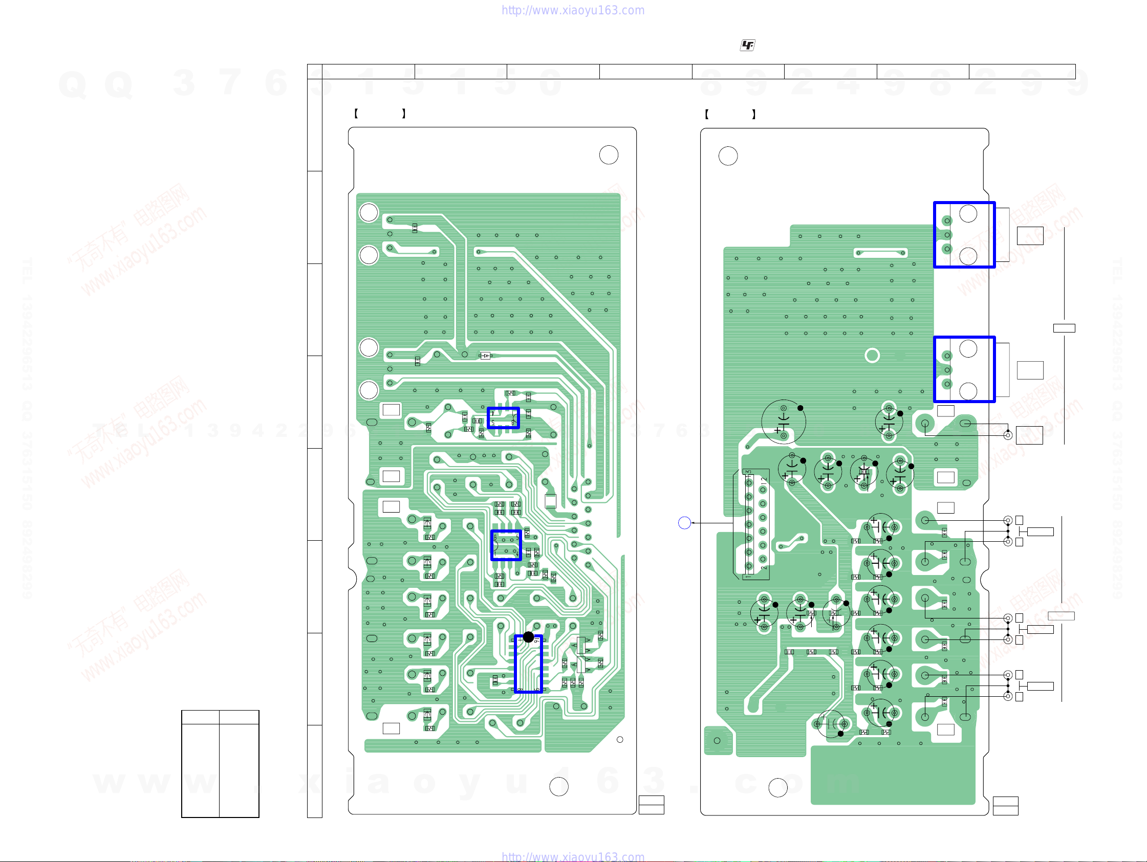
5-5. PRINTED WIRING BOARD – IO Board –
1 2 3 4 5 6 7 8
• See page 15 for Circuit Boards Location.
: Uses unleaded solder.
Q
Q
3
7
6
3
1
IO BOARD
A
B
TEL 13942296513 QQ 376315150 892498299
C
D
T
E
w
L
w
1
3
9
• Semiconductor
Location
Ref. No. Location
D1700 C-2
IC1600 F-2
IC1700 B-7
IC1701 D-7
IC1702 D-2
IC1710 G-3
w
Q1710 G-3
Q1711 G-3
4
.
2
2
E
F
G
H
x
9
6
i
5
a
5
(COMPONENT SIDE)
C1700
C1701
R1701
1
3
FB1701
R1707
FB1700
R1706
FB1705
R1711
FB1704
R1710
FB1703
R1709
FB1702
R1708
o
1
C1704
C1705
R1702
IC1600
C1723
y
5
D1700
IC1702
R1703
R1604
C1602
R1602
C1651
IC1710
R1705
R1610
u
R1652
C1601
C1441
C1652
0
C1708
C1707
R1704
R1651
L1603
R1605
R1654
R1601
R1728
1
Q
R1729
R1730
Q
Q1711
Q1710
R1732
E
E
6
R1733
R1731
1-869-118-
3
7
3
11, 12, 13
(11, 12, 13)
6
A
MAIN
BOARD
CNS198
(Page 21)
.
8
IO BOARD
1
3
9
(CONDUCTOR SIDE)
1
5
CNS197
C1726
C1722
c
C1706
C1608
o
2
5
C1724
R1725
R1727
0
C1655
4
R1716
C1715
R1715
C1727
C1720
R1712
R1724
C1719
R1726
R1714
C1718
R1713
C1725
m
8
C1604
C1603
R1717
9
9
C1716
C1717
R1723
C1703
R1722
R1721
R1718
R1720
C1605
R1719
2
IC1700
IC1701
9
C1710
C1709
C1714
C1713
C1712
C1711
1-869-118-
2
8
8
3
1
3
1
4
2
11, 12, 13
(11, 12, 13)
9
OPT IN
SA-CD/CD
OPT IN
VIDEO 2
J1700
COAX IN
9
DVD
L
SA-CD/CD
R
L
VIDEO 2
R
L
VIDEO 1
R
9
TEL 13942296513 QQ 376315150 892498299
DIGITAL
9
J1710
AUDIO IN
STR-KS1000
1616
5-6. PRINTED WIRING BOARD – ADCC Board –
1 2 3 4 5
• See page 15 for Circuit Boards Location.
STR-KS1000
Ver. 1.2
: Uses unleaded solder.
Q
TEL 13942296513 QQ 376315150 892498299
Q
ADCC BOARD
A
B
R2009
C2015
C
T
D
E
R2008
R2007
L
3
C2009
R2010
D863
IC2000
R2002
R2005
C2003
C2005
C2006
R2006
1
7
(COMPONENT SIDE)
D864
R2011
R2012
C2008
R2003
R2001
R2004
3
9
4
C2017
6
2
2
3
(CHASSIS)
9
BOARD
CNP196
(Page 21)
1
(CHASSIS)
6
B
MAIN
5
ADCC BOARD
C2011
C2002
C2001
4
5
1
3
CNP2000
1
1
(CONDUCTOR SIDE)
R2013
C2016
R2014
C2004
C2010
R2015
BR1
5
C2007
1
2
5
0
J2000
AUTO
Q
CAL MIC
Q
3
7
6
8
3
1
9
5
0
4
8
9
9
2
8
4
9
2
8
2
9
9
9
TEL 13942296513 QQ 376315150 892498299
9
E
w
w
w
1-869-116-
.
11, 12, 13
(11, 12, 13)
x
i
a
(CHASSIS)
o
BR2
y
1-869-116-
u
11, 12, 13
(11, 12, 13)
1
6
3
.
c
o
m
STR-KS1000
1717

STR-KS1000
Ver. 1.2
5-7. SCHEMATIC DIAGRAM – IO Section –
3
7
9
4
J1710
AUDIO IN
6
6P
DIGITAL
2
SA-CD/CD
VIDEO 2
VIDEO 1
OPT IN
SA-CD/CD
OPT IN
VIDEO 2
J1700
1P
COAX IN
DVD
2
3
9
L
R
L
R
L
R
Q
Q
3
TEL 13942296513 QQ 376315150 892498299
T
E
L
1
1
OPTICAL RECEIVER
6
5
IC1700
TORX147L
IC1701
TORX147L
1
• See page 34 for IC Block Diagrams.
5
C1700
0.1
C1701
0.1
C1709
3
C1710
100p
C1711
100p
C1712
100p
C1713
100p
C1714
100p
R1701
C1703
C1704
75
22
50V
0.1
1
OPTICAL RECEIVER
R1702
1k
FB1700
FB1701
FB1702
FB1703
FB1704
FB1705
R1706
R1707
R1708
R1709
R1710
5
SCHMIT TRIGGER
GND
47k
47k
47k
47k
47k
R1712
R1713
R1714
R1715
R1716
C1715
10 50V
1k100p
C1716
10 50V
1k
C1717
10 50V
1k
C1718
10 50V
1k
C1719
10 50V
1k
C1720R1711
10 50V1k
47k
47k
47k
R1719
R1720
R1721
47k
R1722
47k
R1718
0
IC1702
TC7WU04F
(TE12R)
47k
R1717
47k
R1723
R1704
0
R1728
4
C1603C1604
0.1100
16V
R1610
4.7k
C1652
220p
10k
R1732
10k
R1730
R1729
100
100
R1654
10k
R1601C1441
10k0.0033
C1726
100
16V
8
Q1710,1711
INVERTER
R1605
4.7k
C1651R1602
220p470
9
9
L1603
10µH
C1608
10
50V
C1655
10
50V
C1605
10
50V
2
10 50V
C1725
Q1710
DTC124EKA-T146
Q1711
DTC124EKA-T146
8
4
BUFFER
IC1600
NJM4565M(TE2)
VCC
1
2
GND
5
C1601
220p
R1727
IC1710
10k
1
R2
9
5
8
D1700
1SS355WTE-17
560k
C1706
Q
C1707 C1708
1000
0.1 47p
6.3V
R1705
100
Q
R1724
10k
0.1
R1725 C1723
C1722
3
10k 0.1
R1651
10k
C1724
R1652
10k
C1602
220p
R1604
470
R1726
10k
100
16V
3
6
7
ANALOG INPUT SELECT
MC14052 BD
C1705R1703
1p22k
VCC
9
2
8
R1731
10k
R1733
10k
CNS197
2
TUNER_L
TUNER_R
OPT1
OPT2
COAX
DGND
AGND
13P
3.3V
L_IN
R_IN
IO_A
IO_B
9
9V
9
9
TEL 13942296513 QQ 376315150 892498299
9
(Page 23)
STR-KS1000
w
w
w
.
R2014
4.7k
C2007
C2017
0.1
R2015
2.2k
R2016 C2003
J2001
AUTO
CAL MIC (CHASSIS)
x
i
2.2k 47
a
C2008
1
50V 1
R2008
1k
o
C2016
100p
C2010
R2009
R2011
560k
56p
10k
y
0.033
IC2001
NJM4565TE
GND
u
VCC
R2007
MIC AMP
1
10k
C2006
R2006
6
33p
C2005
50V
D864
C2018
C2002
16V
R2012
C2012
0.47
R2003
R2005
4.7k
1k
1M
R2004
10k
C2009
0.033
R2010
10k
3
R2002
4.7k
C2011
1
50V
D863
1SS355WTE-17
C2004
0.1
1SS355WTE-17
.
0.1
47
16V
18k
c
50V
CNP2001
R2013
22k
ADCC2
4P
9V
AGND
NC
o
1818
(Page 25)
m
C1727
10 50V
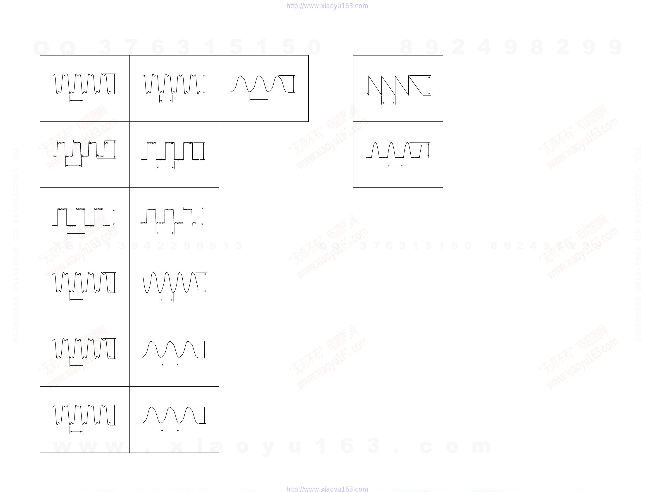
• Waveforms
– MAIN Board –
Q
Q
IC1301 qd (CKOUT)
1
3
7
7
6
IC1501 qf (SCKOUT)
3
1
qd
5
IC305 2
1
5
0
– DISPLAY Board –
IC700 5 (OSC)
wa
8
9
2
4
9
8
2
STR-KS1000
9
9
4 Vp-p
81.5 ns
1 V/DIV, 50 ns/DIV
IC1301 qf (BCK)
2
TEL 13942296513 QQ 376315150 892498299
326 ns
1 V/DIV, 100 ns/DIV
IC1301 qg (LRCK)
3
20.8 µs
1 V/DIV, 10 µs/DIV
T
E
IC1301 w; (XMCK)
4
L
4 Vp-p
3.9 Vp-p
1
3
8
9
9
q;
81.5 ns
1 V/DIV, 50 ns/DIV
IC1501 ql (LRCKO)
20.8 µs
1 V/DIV, 10 µs/DIV
IC1501 w; (BCKO)
326 ns
1 V/DIV, 100 ns/DIV
4
2
2
IC1601 id (X1)
4.3 Vp-p
4.3 Vp-p
4.7 Vp-p
9
6
5
1
20.3 µs
200 mV/DIV, 10 ns/DIV
3
0.7 Vp-p
Q
Q
2.4 µs
1 V/DIV, 1 µs/DIV
Q700, 701 (Collector)
ws
13.1 µs
5 V/DIV, 5 µs/DIV
6
7
3
3
2.2 Vp-p
20.8 Vp-p
5
1
1
5
0
8
9
2
4
9
8
2
9
TEL 13942296513 QQ 376315150 892498299
9
81.5 ns
1 V/DIV, 50 ns/DIV
IC1301 wa (XOUT)
5
81.5 ns
1 V/DIV, 50 ns/DIV
IC1501 qs (MCLK2)
6
72 ns
1 V/DIV, 50 ns/DIV
w
w
4.3 Vp-p
4.3 Vp-p
4.5 Vp-p
w
41.7 ns
1 V/DIV, 20 ns/DIV
IC109 qf (XFSOOUT)
qa
20.8 µs
1 V/DIV, 10 ns/DIV
IC108 qf (XFSOOUT)
qs
20.8 µs
1 V/DIV, 10 ns/DIV
.
x
3.4 Vp-p
3 Vp-p
3 Vp-p
i
a
o
y
u
1
6
3
.
c
o
m
STR-KS1000
1919

STR-KS1000
Ver. 1.2
5-8. PRINTED WIRING BOARD – MAIN Board (Component Side) –
• See page 15 for Circuit Boards Location.
: Uses unleaded solder.
1 2 3 4 5 6 7 8 9 10 11
3
MAIN BOARD
1
(COMPONENT SIDE)
Q
Q
• Semiconductor
Location
3
Ref. No. Location
D914 G-10
7
6
A
D915 G-10
D923 J-10
D925 J-10
D926 J-10
D932 D-9
D1301 G-4
D1500 G-4
D1501 G-4
B
D1502 G-4
D1600 F-3
D1661 F-3
IC101 E-7
IC102 E-6
TEL 13942296513 QQ 376315150 892498299
IC103 E-5
C
IC104 E-5
IC105 E-4
IC106 E-3
IC107 E-2
IC108 F-6
IC109 F-5
IC110 F-3
D
IC303 E-8
IC305 F-6
IC1111 J-4
IC1131 I-3
IC1301 H-3
IC1501 H-5
IC1502 H-6
IC1503 G-4
IC1601 I-4
IC1602 G-3
E
R120
IC1651 H-2
T
E
L
1
Q943 E-9
3
9
4
2
2
9
6
Q945 J-6
Q946 J-6
F
Q947 E-9
G
FB1102
7
8
0
1
R
6
7
0
1
R
R1260
R1261
i
w
w
w
.
H
4
1
3
1
B
I
F
J
x
K
5
C274
R167
C273
C272
IC107
R147
C218
R128
R119
C146
1
3
R319
L1604
C1067
5
R157
C147
C1068
IC1651
L1600
a
(E51, SP, MY, AR)
2
5
2
1
R
1
5
2
1
R
JR1202
FB1315
C1065
C1066
1
R
R
(AEP, UK)
R1145
R1164
(AEP, UK)
(E51, SP, MY, AR)
(AEP, UK)
o
0
C1139
1
8
IC106
C200
R166
R384
7
4
3
R
R317
R1618
C
2
7
6
1
R
IC1131
6
R1158
2
7
0
R1175
1
1
C
R1058
R1059
R156
5
4
3
R
R316
R353
5
6
1
2
7
1
6
1
C
10
5
7
6
1
C
X1301
8
2
1
1
R
R
8
0
C271
R146
2
0
8
8
3
4
12
R
R
13
IC110
24
25
D1661
C1658
9
7
0
6
1
R
R1671
R510
R1310
IC1301
8
3
5
R
L503
R1159
1
1
R
7
0
1
1
C
1
R
C1124
0
9
1
1
R
R
6
3
6
1
1
1
R
1
R118
R117
1
8
3
0
R379
R
8
3
R
R383
1
36
R326
R356
D1600
C1674
20
11
C1659
L1605
C1309
C1310
25
36
37 48
R1318
R1311
2
0
3
1
R1079
FB
R1092
(EXCEPT E51, AR)
31
7
5
1
1
R
6
5
1
2
4
R1220
50
5
3
6
1
4
0
1
1
C
9
2
5
1
0
1
1
R
1
C
4
2
y
C210 C209
C199
R145
R165
R155
C145
48
37
8
2
3
R
C406
IC1602
R1608
R1607
R1606
5
9
0
0
3
3
1
1
R
FB
R1308
1324
12
R1304
JR1102
JR1101
1
R1700
R1362
R1313
R1312
(E51, AR)
R1078
R1081
R1089
R1082
3
4
8
8
0
0
1
1
R
R
IC1601
9
1
8
7
3
2
9
1
1
8
8
7
7
6
7
1
1
1
1
1
1
1
R
1
1
1
1
1
1
R
R
R
R
R
R
5
C105
R116
JR1104
7
1
0
0
3
3
1
1
6
R
D
0
3
1
R
3
0
3
1
C1304
C
C1302
R1316
R1315
1
5
1
1
R
1
0
2
5
1
1
1
1
R
R
5
0
5
3
0
1
8
5
7
1
1
0
1
R
1
1
1
R
R
R
u
1
5
5
0
5
3
1
1
B
F
R
1
0
3
1
0
6
3
1
R
R1303
9
4
1
1
R
6
8
3
1
2
1
1
R
1
R
C1138
IC1111
C114
R329
B
F
4
4
1
1
R
3
4
1
1
R
R
130
100
81
8051
2
2
1
1
R
3
R115
2
1
3
R
R1508
R
2
4
1
1
R
4
0
1
9
8
1
1
R
1
45
0
C208
C198
R164
C144
IC109
13
24
8
1
3
R
0
1
3
R
D1502
D1500
9
0
5
1
6
7
3
3
1
1
1
1
R
R
4
1
0
1
1
X
7
7
2
0
1
1
1
1
1
R
C
R
6
1
1
R
7
3
1
1
C
C207 C206 C205 C204 C203
IC104IC105
R114 R113
6
7
3
R
1
36
R327
4
4
5
1
3
3
R
R
3
1
3
R
1
3
R
3
0
5
1
4
R
0
5
1
R
48
37
R
1
1
3
R
5
R375
Q
R
7
5
3
C
2
0
3
R
2
0
5
1
R
6
5
5
1
R
C190
R163
C143
4
2
3
5
0
4
0
0
3
R
C1520
3
0
5
1
FB
R1523
R1515
31
8
7
3
R
12
25
R
3
0
4
C
R144
R154
Q
4
4
3
D1501
6
0
5
1
R
30
7
7
3
R
5
0
3
R
5
0
5
1
R
IC1501
60
0
7
R1511
5
1
R
R1135
R1134
R1140
R1042
R1041
5
2
1
1
R
7
6
1
6
2
1
1
8
R
1
R1183
R1166
R1221
R
R
R1163
1
8
1
5
1
C
6
1
1
4
8
1
1
R
5
1
1
1
6
IC103
R153
3
0
3
R
1
5
3
R
X1502
1
120
91
9061
1
7
5
1
R
2
7
5
1
R
4
0
3
R
R143
4
0
4
C
1
C
3
7
5
1
R
IC108
R322
C
6
0
3
R
1
1
5
R
R1548
R1549
R1550
4
7
5
1
R
R112
R325
2
0
4
8
0
3
R
C1521
4
1
5
1
0
0
5
1
B
R
2
0
5
1
B
R
3
6
4
3
R
3
0
5
1
B
R
R111
12
13
24
8
4
3
R
1
0
5
1
B
R
C189
R162
R372
4
3
7
7
3
3
R
R
25
R323
5
5
3
R
IC1502
R1542
4
0
5
1
B
R
1
4
9
R
R958
5
9
R
3
IC102
2
4
1
C
R371
1
7
36
8
5
3
R
R1528
G
7
S
R142
48
37
5
0
5
1
B
R
D915
9
2
8
R911
R919
1
1
9
C
7
0
9
R
R918
9
9
2
1-869-115-
9
TEL 13942296513 QQ 376315150 892498299
9
11, 12
(11, 12)
0
R938
D932
Q947
1
5
9
R
2
5
9
R
m
4
0
7
4
3
9
9
R
R
R949
Q943
E
E
8
9
9
8
4
2
0
9
1
0
9
9
R
R
D914
D923
D925
3
6
2
2
9
9
C
D
8
C202
9
0
5
3
C
C201
IC101
R109
R141
C188
C141
1
8
3
C
3
R108
R151
1
R946
R948
C119
C374
5
6
6
9
R
c
R161
R110
2
5
1
X450
R
6
9
3
R
13
R393
45
6
IC305
R321
0
2
3
R
5
5
5
1
R
1
4
5
1
R
6
0
5
1
B
R
8
7
9
R
6
G
5
4
D
4
D
9
9
Q
S
Q
9
6
9
R
L947
.
2
2
3
4
5
7
7
7
7
4
4
4
4
R
R
R
R
R965
R932
R931
1
3
5
4
1
IC303
o
5
1
4
9
L
STR-KS1000
2020
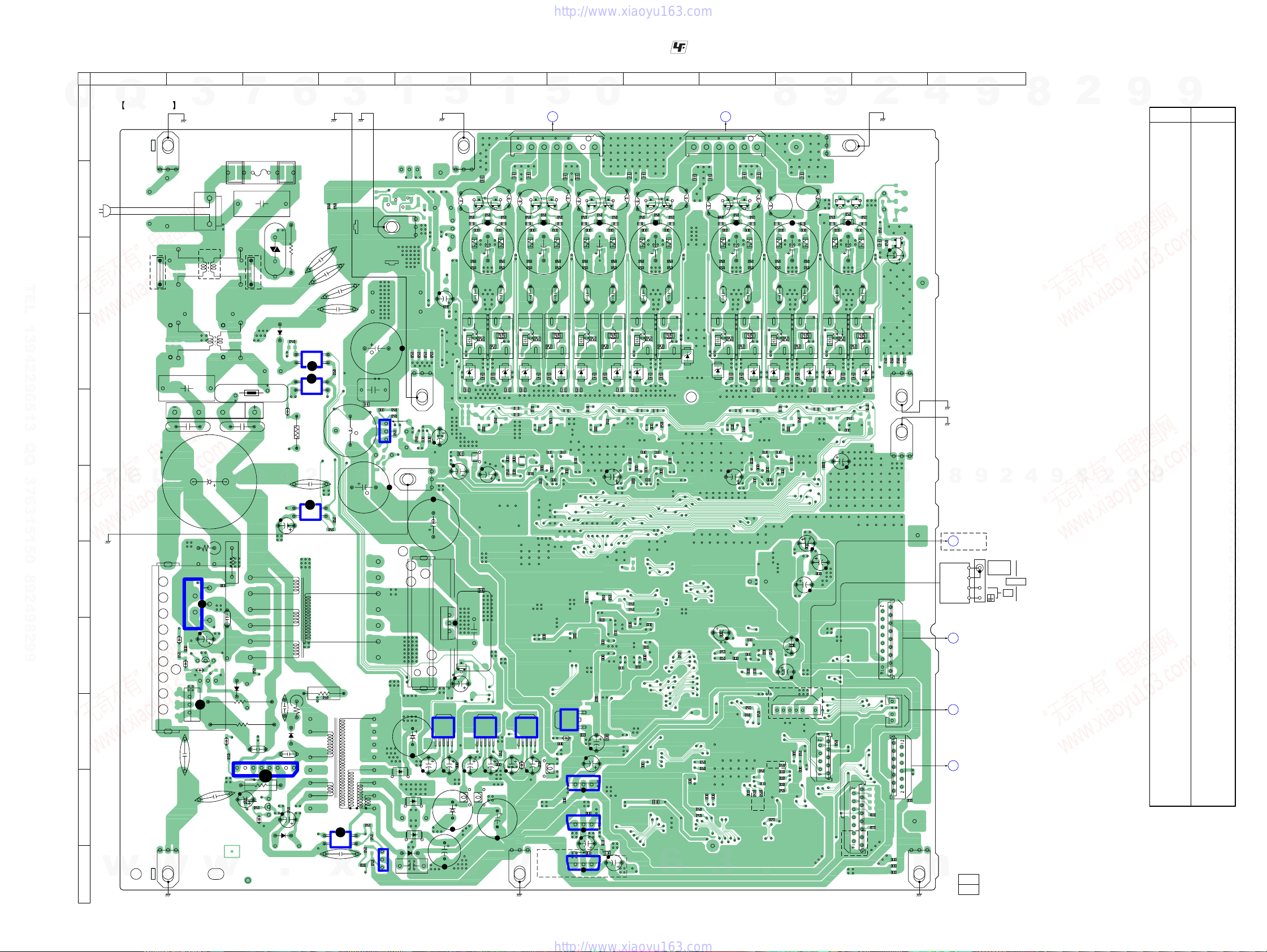
5-9. PRINTED WIRING BOARD – MAIN Board (Conductor Side) –
• See page 15 for Circuit Boards Location.
STR-KS1000
Ver. 1.2
: Uses unleaded solder.
1 2 3 4 5 6 7 8 9 10 11 12
LF902
C912
D901
3
7
(E51, AR)
TH901
C920
F901
9
6
FH901FH902
C901
1
0
1
9
0
R
9
D
R
V
2
0
9
W
J
4
0
9
D
D
9
0
9
4
R915
K
A
C
E
8
0
9
R
C963
PC904
PC903
C938
2
3
(CHASSIS)(CHASSIS)
4
0
2
3
9
9
R
R
C964
C965
C966
E
C
0
6
9
R
A
K
1
3
9
L
2
9
PC901
T901
MAIN POWER
TRANSFORMER
R967
C
E
A
K
5
3
9
R
R934
R968
T902
SUB POWER
TRANSFORMER
PC902
C928
x
R956
C952
C
E
C910
4
1
9
R
C909
1
6
0
5
9
C
E
5
0
9
R
5
0
9
D
1
2
R903
R904
0
1
9
D
C905
5
2
9
R
IC921
R927
C924
R923
1
9
2
C
9
R
1
2
9
D
C925
18
C929
6
2
2
E
2
9
9
1
2
9
Q
R
R
C922
4
2
9
D
D922
.
Q
Q
MAIN BOARD
A
B
(AC IN)
(E51, AR)
1
0
TEL 13942296513 QQ 376315150 892498299
C
9
JW
3
(CONDUCTOR SIDE)
(CHASSIS)
EB901
(EXCEPT E51, AR)
1
CN901
2
LF901
D
C902
E
T
E
L
C918
C903
1
F
7
0
9
D
6
0
9
R
IC901
2
4
C908
7
0
9
C
6
0
9
D
3
1
9
D
Q901
A
K
D908
R912
(CHASSIS)
G
H
I
3
1
9
C
J
EB902
K
w
w
w
1
EB909
C934
C939
C936
R933
C937
R936
1
9
3
3
9
R
C933
6
D943
D942
9
4
5
R
5
9
R
3
5
9
IC951
5
i
D944
D941
1
3
A
K
R
STR-KS1000
5
EB908
Q101
1
0
1
L
E
R361
R401
C281
C251
1
1
2
R
R490
R459
C366
1
1
2
C
C367
1
2
1
L
1
6
1
C
FB301
3
C329
1
Q961
C961
9
2
4
9
L
o
R191
1
0
1
D
C101
1
0
3
L
C380
C935
1
3
9
C
E
IC942
5
5
9
C
5
4
9
C
5
4
9
L
7
9
8
6
7
7
7
7
4
4
4
4
R
R
R
R
EB911
IC931
5
7
3
C
0
0
4
R
8
1
6
7
3
3
C
C
EB903
5
1
2
3
9
C
3
9
D
A
K
A
IC943
0
4
9
C
15 15 15
8
4
4
9
9
C
C
4
4
9
C
6
4
9
C
a
C953
1
5
7
2
C
Q102
C391
C261
1
L
R201
1
5
1
C
1
3
1
C
7
4
9
C
1
4
9
C
R402
9
1
C
R489
3
1
C171
1
8
1
C
1
4
2
R
9
R
C954
1
1
1
L
E
C282
1
2
2
R
R458
1
2
2
C
1
C111
R131
R171
4
8
3
C
4
9
3
R
3
4
9
C
y
6
7
2
C
2
4
EB904
7
R403
C283
1
0
2
D
C102
3
8
3
C
2
8
3
C
IC941
R457
2
1
2
C
2
0
3
L
5
4
9
D
Q103
2
0
1
L
C252
2
1
2
R
2
1
L
2
6
1
C
C303
C
7
7
2
C
E
R488 R487
2
R192
2
5
1
2
0
C
1
D
2
3
1
R
2
3
1
C
C304
2
0
3
C
0
1
3
C
1
5
9
C
3
4
9
IC1712
(AEP, UK)
IC1711
5
SPEAKER BOARD
E
CN303
Q104
E
R404
R362
C392
C262
2
9
1
C
R456
2
3
1
L
C172
R202
2
8
1
C
C112
2
4
2
R
C305
1
0
3
C
C309
9
1
5
1
C
2
D1006
0
5
9
L
1
5
7
1
C
C1731
u
0
(Page 22) (Page 22)
CNP510
1
E
R363
3
5
1
C
3
3
1
C
0
5
1
3
0
1
Q106
E
R406
C393
C263
3
9
1
C
R460
R491
1
L
C173
R203
3
8
1
C
3
4
2
R
C332
1
2
0
1
5
5
1
1
R
R
1
0
5
1
C
4
1
5
1
C
3
1
5
1
C
2
1
0
5
1
B
5
F
IC1033
3
0
2
1
R
J
FB1313
1
C1732
8
9
2
C
3
1
1
L
R407
C287
C286
C254
3
4
2
1
2
2
R
R
R461 R462
R492
3
4
2
1
2
2
C
C
3
3
1
L
4
6
1
C
3
0
2
D
C104
R173
R134
C314
3
1
3
C
C
2
1
3
C
Q
Q
9
1
3
C
R1513
R566
3
0
5
1
C
C1507
C1508
3
6
1
1
C
FB1101
9
8
9
7
2
2
C
C
2
3
1
0
1
1
L
L
R405
C285
C284
C253
3
2
1
2
2
2
R
R
R464
R463
2
3
2
1
2
2
C
C
1
L
3
6
1
C
2
0
2
D
C103 C113
R172
3
3
1
R
6
0
3
C
8
0
3
C
2
2
5
1
C
C1034
C1037
C1750
C1729
C1728
Q105
3
2
R193
3
0
1
D
9
0
5
1
C
C1510
FB
3
IC1034
1
C
13
13
13
4
0
1
L
2
3
C318
Q107
4
1
7
9
2
C
R194
4
0
1
D
R174
1
C1505
6
0
5
1
C
E
R364
C394
C264
4
9
1
C
C174
R204
4
5
1
C
4
3
1
C
C315
C1504
6
SPEAKER BOARD
8
F
CNP500
6
CN302
8
6
6
9
2
2
C
C
4
Q108
1
1
5
L
0
E
R408
C288
4
2
2
R
R493
4
2
2
C
4
3
1
L
4
8
1
C
4
4
2
R
6
1
3
C
7
1
3
C
1
1
R
2
1
C
1
L
R409
C289
C255
5
1
2
R
R450
R481
5
1
2
C
2
1
L
5
6
1
C
4
0
2
D
5
0
1
D
7
3
C1306
R1302
R1043
R1049
0
9
3
2
1
1
1
1
C
C
3
9
R1180
R1179
0
9
3
2121
1
9
9
7
6
2
2
C
C
Q109
5
1
1
L
Q110
E
E
R365
R410
C395
C290
C265
5
2
2
R
5
9
1
C
R451
R483 R484
R482
5
2
2
C
5
5
3
1
L
C175
R195
R205
5
0
2
D
5
5
5
8
1
1
C
C
C115
R175R135
5
4
2
R
5
3
1
C
C323
2
2
3
1
2
3
C
C
C1301R1301
5
0
3
1
C
R1161
R1162
C
C
C327
6
8
2
3
C
C536
2
1
3
1
C
C1314
3
5
1
1
3
3
1
1
C
C
0
6
1
1
R
(E51, SP, MY, AR)
R1100
C1620
2
0
1
1
3
4
9
9
0
0
1
1
R
R
(E51, SP, MY, AR)
R1088
C335
.
C106
R
3
R1095
C1120
C1125
C1121
D
1
0
2
3
C291
C256
6
1
2
R
R452
6
1
2
C
L
6
6
1
C
6
0
1
6
3
C324
4
1
3
1
R
6
R1165
6
0
1
L
6
2
1
R196
6
5
1
C
1
C
5
2
3
C
6
2
3
C
C1656
C1673
C1331
C542
(EXCEPT E51)
C
R206
6
3
CNP195
2
1
1
0
8
2
C
C292
C176
1
3
2
1
1
C
2
C266
6
9
1
C
L
C1670
R453
3
1
6
8
1
C
6
4
2
R
3
7
0
1
R
(NC)
6
6
0
2
D
C116
0
3
3
1
C
c
6
2
2
R
R176
1
6
1
1
L
6
2
2
C
C1671
C293
R
N
C
9
EB906
R411
C257
7
1
2
C
1
L
7
6
1
C
C107
R137
9
0
3
5
4
5
6
1
C
2
9
1
S
Q111
C396
7
1
2
R
2
R197
7
0
1
D
C120
• Semiconductor
Location
9
Ref. No. Location
D101 D-5
D102 D-6
D103 D-7
D104 D-8
D105 D-9
D106 D-9
D107 D-10
D201 D-6
D202 D-7
D203 D-7
D204 D-8
D205 D-9
D206 D-10
D207 D-11
D901 E-2
D904 D-3
D905 H-2
D906 H-2
D907 H-2
D908 H-2
D909 E-3
D910 I-2
D913 I-2
D921 I-3
D922 J-3
D924 J-3
D931 H-5
D941 K-5
D942 J-5
D943 J-5
D944 J-5
D945 I-6
D1006 I-7
IC901 G-2
9
9
IC921 I-3
IC931 E-4
IC941 I-6
IC942 I-6
IC943 I-5
IC951 K-4
IC1033 J-7
IC1034 I-7
IC1711 K-7
IC1712 J-7
Q101 B-6
Q102 B-6
Q103 B-6
Q104 B-7
Q105 B-7
Q106 B-7
Q107 B-8
Q108 B-8
Q109 B-9
Q110 B-9
Q111 B-10
Q112 B-11
Q301 C-11
Q901 H-2
Q921 J-3
Q961 H-5
PC901 F-3
PC902 J-4
PC903 D-3
PC904 D-3
9
TEL 13942296513 QQ 376315150 892498299
9
2
8
2
5
1
9
0
3
3
R
Q
E
C158
9
6
4
R
EB910
EB907
0
3
6
9
1
P
1
3
1
S
N
C
C1153
C1150
C1151
1
0
7
7
4
4
R
R
8
9
C1152
EB905
m
(CHASSIS)(CHASSIS)(CHASSIS)
4
(CHASSIS)
(CHASSIS)
(EXCEPT E51)
(Page 17)
(Page 16)
1-869-115-
8
HDMI BOARD
D
CN5004
TUNER
C
DISPLAY
BOARD
CNS703
(Page 32)
B
ADCC
BOARD
CNP2000
A
IO
BOARD
CNS197
11, 12
(11, 12)
9
9
(Page 30)
FM 75Ω
COAXIAL
2
8
4
ANTENNA
AM
2
(CHASSIS)(CHASSIS)
Q112
E
E
R366
R412
C294
9
3
1
R
C267
5
8
3
C
7
9
1
7
C
2
2
R
7
2
2
C
7
7
3
1
L
C177
R207
7
5
1
C
R247
C137
1
7
9
0
1
R
S
N
C
(AEP, UK)
8
6
4
R
7
0
7
2
8
D
1
C
C117
7
7
1
R
5
9
1
S
N
C
N
C
5
9
1
C1252
C1251
o
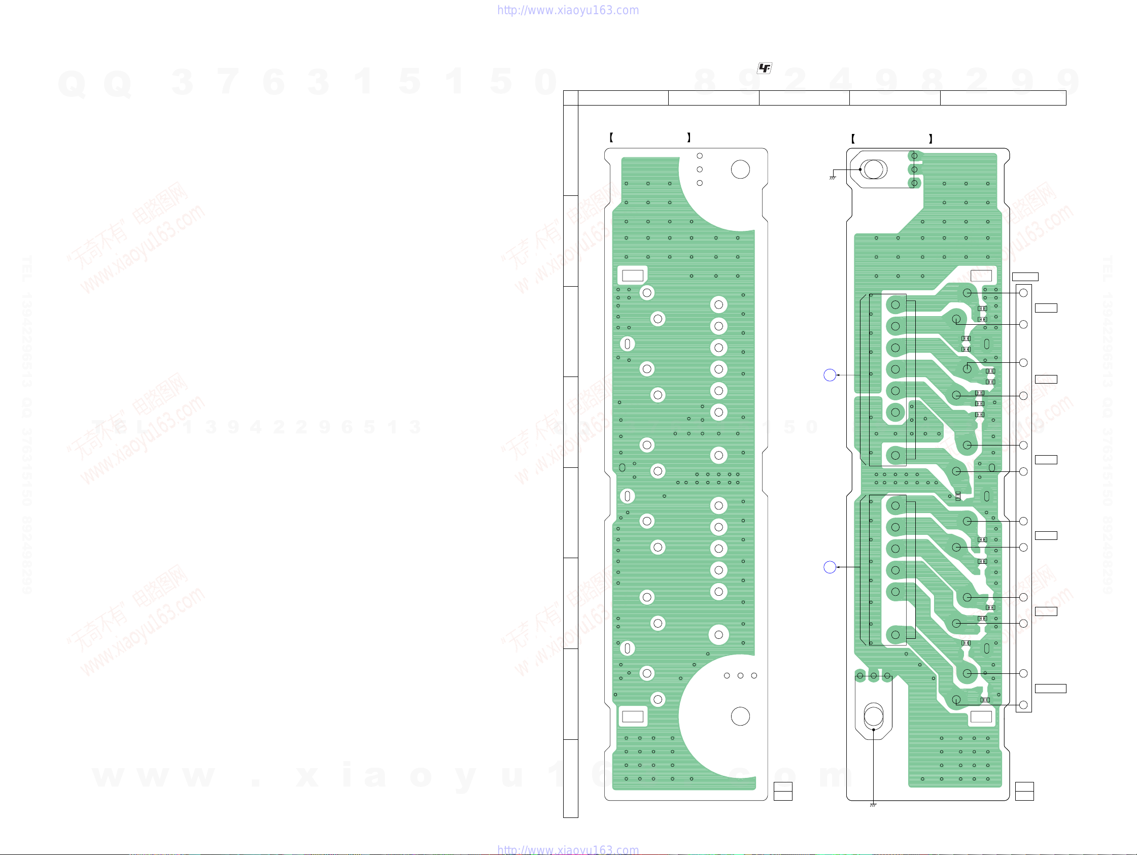
STR-KS1000
Ver. 1.1
5-10. PRINTED WIRING BOARD – SPEAKER Board –
3
7
9
4
6
2
2
3
9
Q
TEL 13942296513 QQ 376315150 892498299
T
Q
E
L
3
1
1
6
5
1
5
3
1
5
• See page 15 for Circuit Boards Location.
0
Q
A
B
C
D
Q
1 2 3 4 5
SPEAKER BOARD (COMPONENT SIDE)
6
7
3
8
3
1
9
5
: Uses unleaded solder.
(CHASSIS)
BOARD
(Page 21)
0
4
E
MAIN
CN303
1
2
5
9
C515
C500
2
C514
C501
C512
C503
C513
C502
C505
8
2
EP501
2
8
4
9
SPEAKER BOARD (CONDUCTOR SIDE)
7
CNP510
9
8
1
9
TM500
SPEAKERS
–
+
–
+
9
–
+
9
TEL 13942296513 QQ 376315150 892498299
FRONT L
FRONT R
9
SURR R
STR-KS1000
w
w
w
.
x
i
a
o
y
E
F
G
u
1
2222
H
6
3
.
c
1-869-117-
o
11, 12
(11, 12)
F
MAIN
BOARD
CN302
(Page 21)
m
EP500
(CHASSIS)
6
CNP500
1
C511
C504
C507
C506
C508
C510
C509
1-869-117-
–
SURR L
+
–
CENTER
+
–
SUB WOOFER
+
11, 12
(11, 12)
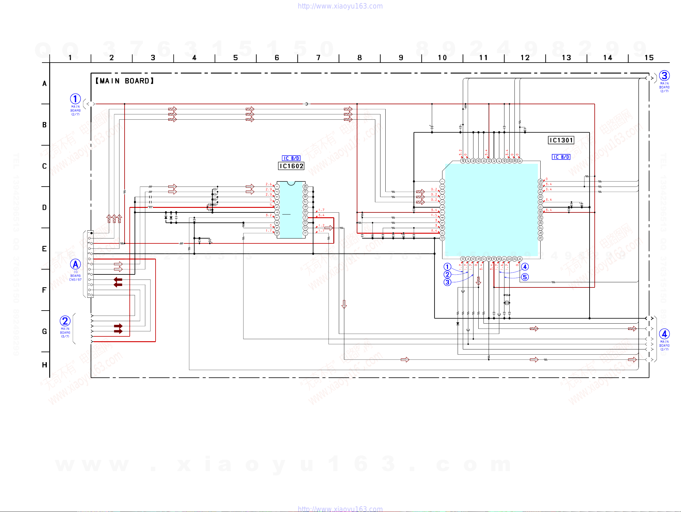
STR-KS1000
Ver. 1.2
5-11. SCHEMATIC DIAGRAM – MAIN Section (1/7) –
Q
Q
(Page 24)
3
A1
7
6
(1/7)
• See page 19 for Waveforms. • See page 34 for IC Block Diagrams.
3
1
TEL 13942296513 QQ 376315150 892498299
R1609
470
R1618
C1654
C1671
L1604
D1600
1SS355WTE-17
4
470
0.1
0.1
10µH
D1661
1SS355WTE-17
2
C1674
0.001
L1605
R1672
2
C1673
47 10V
C1672
0.1
C1675
0.01
C1653
10
C1659
50V
0.1
0
100
9
6
T
(Page 18)
(Page 25)
E
TUNER_R
TUNER_L
L
IO_B
IO_A
L503
0
CNS198
13P
OPT1
OPT2
3.3V
COAX
DGND
9V
L_IN
R_IN
AGND
TUNER_L
TUNER_R
IO_A
IO_B
A5V
9V
1
R538
0
3
9
C1657
C1658
C1656
C1670
5
0.01
0.01
10 50V
10 50V
1
5
R1671
0
R510
100
3
1
A/D CONVERTER
IC1602
PCM1803DBR
LIN
MODE1
RIN
MODE0
V_REF_1
V_REF2
VCC
AGND
PDWN
BYPASS
FSYNC
LRCK
5
FMT1
FMT0
OSR
SCKI
VDD
DGND
DOUT
BCK
FB1302
0
R1606
100
Q
R1302
4.7k
R1607
Q
9
C1331
2
9
9
A8
(Page 24)
TEL 13942296513 QQ 376315150 892498299
R1314
10k
R1315
100
9
100
100
9
DIR_AUDIO
DIR_XSTAE
DIR_DATA0
DIR_D1
DIR_DO
AD_RST
ERR
A2
A7
A3
A4
A6
(Page
A5
24)
R1313
C1330
10
0.1
50V
C1312
0.1
8
R1312
2
DOSEL1
LC89056W-E
DATAO
100
1309
R
DOSEL0
XSTATE
0
R1608
IC1301
2.2k
DVDD
DGND
4
DGND
DVDD
0.1
6
C53
2
JR1104
8
DIGITAL AUDIO
INTERFACE RECEIVER
4
R1311
100
0
9
DIR_CLK
DIR_HCE
.1
0
4
131
C
MODE1
XMCK
8p
1
09
1305
13
FB
C
MODE0
XOUT
XSEL
XIN
8
R1310
1M
X1301
12.288MHz
C1310
18p
CL
EMPHA
R1316
C1313
100p
CE
AUDIO-
100
DI
DO
ERROR
BPSYNC
LOCK
DGND
DVDD
VF
F2
F1
F0
CSFLAG
9
1
9
C542
220
10V
5
D1301
1SS355WTE-17
DISEL
SPDIF
DIN0
DIN1
DIN2
DGND
DVDD
R
VIN
LPF
AVDD
AGND
FB1301
8
100
R1362
R1700
100
R1301
5.6k
1k
C1302
R1303
0.01
C1303 C1305 C1304
33k
0.1 0.1 0.01
3
7
JR1101
JR1102
R1304
C1306
47
16V
6
C1301
0.1
0
0
100
3
1
100
8
30
1
R
DIR_CKSEL1
DIR_XMODE
0.1
5
10k
131
C
1318
R
XMODE
CKOUT
100
100
0
5
136
130
R
R
551
1
FB
2
CKSEL0
CKSEL1
LRCK
BCK
5
390
100
6
7
130
130
R
R
STR-KS1000
w
w
w
.
x
i
a
o
y
u
1
6
2323
3
.
c
o
m
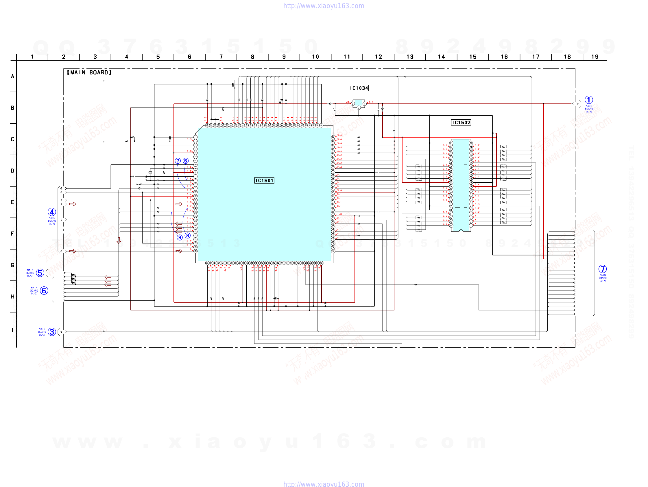
STR-KS1000
Ver. 1.2
5-12. SCHEMATIC DIAGRAM – MAIN Section (2/7) –
(2/7)
7
R1501
100
Q
Q
3
DSP_PM
DSP_RST
• See page 19 for Waveforms. • See page 34 for IC Block Diagrams. • See page 38 for IC Pin Function Description.
6
C1511R1512
3
0.11k
TEL 13942296513 QQ 376315150 892498299
C1521
10p
(Page 25)
(Page 26)
(Page 23)
T
ADCC_INT
LRCKO
D-GND
X1502
13.9MHz
C1520
10p
1
LRCKO
MCKO
LRCKO
BCKO
D1
D2
D3
3
D1
D2
D3
BCKO
MCKO
A2
A3
A4
A5
A6
E
L
A7
1SS355WTE-17
D1
D2
D3
BCKO
SCK
D1502
1SS355WTE-17
D1501
1SS355WTE-17
D1500
9
FB1503
4
2
R1515R1523C1503
1M2200.1
R1513R566
10k10k
R1556
100
100
R1502
100
R1503
R1504
100
R1505
100
R1506
100
2
9
6
1
0.1
C1501
VSS
XRST
EXTIN
LRCK13
VDDI
BCK13
PLOCK
VSS
MCLK1
VDDI
VSS
MCLK2
MS
SCKOUT
LRCKI1
VDDE
BCKI1
SDI1
LRCKO
BCKO
VSS
KFSIO
SDO1
SDO2
SDO3
SDO4
SPDIF
LRCKI2
BCK2
SDI2
VDDI
5
VSS
100
1508
R
5
0.1
1509
C
R1514
10k
SDI3
SDI4
TST2
TST3
GP11
SYNC
1
3
GP12
HCS
HDOUT
HDIN
HCLK
HACN
100
1509
R
1
D1
D4
D2
D0
D3
0.1
14
C15
VDDE
IC1501
CXD9862R
WE0
20
2
1541
R
D5
D2
D4
D3
VSS
WMD1
VDDE
A2
A0
A1
220
220
220
49
48
50
15
15
15
R
R
R
A0
A1
A2
D1
PM
GP13
C1504 C1506C1505
0.1 0.10.1
D0
VSS
DIGITAL AUDIO
SIGNAL PROCESSOR
VS0
OE0
VSS
GP15
VDDI
GP14
00
20
1
2
1542
1555
R
R
5
0.1
0.1
13
10
15
C
C15
D5
VSS
VDDI
VSS
WMD0
PAGE2
0
A8
A5
A3
A7
A4
D7
D6
A6
+1.8V REGULATOR
IC1034
NJM2885DL-I8
OGI
C1034
0.1
C1035
FB1502
220
10V
8
FB1501
9
2
4
9
8
2
9
A1
9
(Page 23)
5
S-RAM
12TLI
NC
NC
A11
A12
A10
A13
A9
A14
A8
A15
NC
WE
D8
D7
D9
D6
D10
D5
D11
D4
VDD
VSS
VSS
VDD
D12
D3
D13
D2
D14
D1
D15
D0
CSBLE
A0
BHE
A1
OE
A7
A2
A6
A3
A5
A4
0
8
C1519
0.1
RB1503
9
100
RB1504
RB1505
RB1506
2
A10
A11
A12
A9
100
D8
D9
D10
D11
100
D12
D13
D14
D15
100
A7
A8
A13
A15
A14
4
9
DIR_CKSEL1
DIR_XMODE
DIR_CLK
DIR_DO
DIR_HCE
8
DIR_D1
DIR_XSTAE
DSP_RST
DIR_DATA0
ACK
DIN
D_CLK
DSP_DO
DSP_HCE
GP12
GP9
DSP_PM
ERR
AD_RST
2
DIR_CKSEL1
DIR_XMODE
DIR_CLK
DIR_DO
9
DIR_HCE
DIR_D1
D-GND
D3.3V
DIR_XSTAE
DSP_XRST
DIR_DATA0
DSP_ACK
DSP_HDIN
DSP_HCLK
DSP_HDOUT
DSP_HCS
DSP_GP12
DSP_GP9
DSP_PM
DIR_ERROR
DSP_BST
AD_RST
9
(Page
25)
TEL 13942296513 QQ 376315150 892498299
D6
PAGE1
D7
PAGE0
A3
TST1
BOOT
VSS
TDI
TCK
XTRST
TMS
TDO
A10
A11
A12
A9
VSS
D8
D9
D10
D11
VDDE
D12
D13
D14
D15
VSS
VDDI
GP8
GP9
GP10
A13
A14
A15
A16
Q
Q
A17
VSS
VDDI
EXLOCK
MOD1
MOD0
BST
3
R1574
R1573
R1572
R1571
R1570
C1507
R1511
R1528
A8
A6
A7
A5
A4
C1522 IC1502
10k
10k
10k
10k
10k
0.1
100
220
7
0.1 1S61WV6416BLL
A0
A1
3
A2
D0
D1
D2
D3
D4
D5
D6
D7
A3
A4
A5
A6
1
RB1500
RB1501
RB1502
100
100
100
5
R1130
C1508
C1518
6
A10
A11
A12
A9
0.1
D8
D9
D10
D11
D12
D13
D14
D15
0.1
A13
A14
A15
1
100
(Page 23)
STR-KS1000
A8
w
w
w
.
x
i
ACK
DIN
a
D_CLK
DSP_DO
DSP_HCE
GP12
o
y
ERR
u
1
6
2424
3
DIR_AUDIO
GP9
.
c
o
m
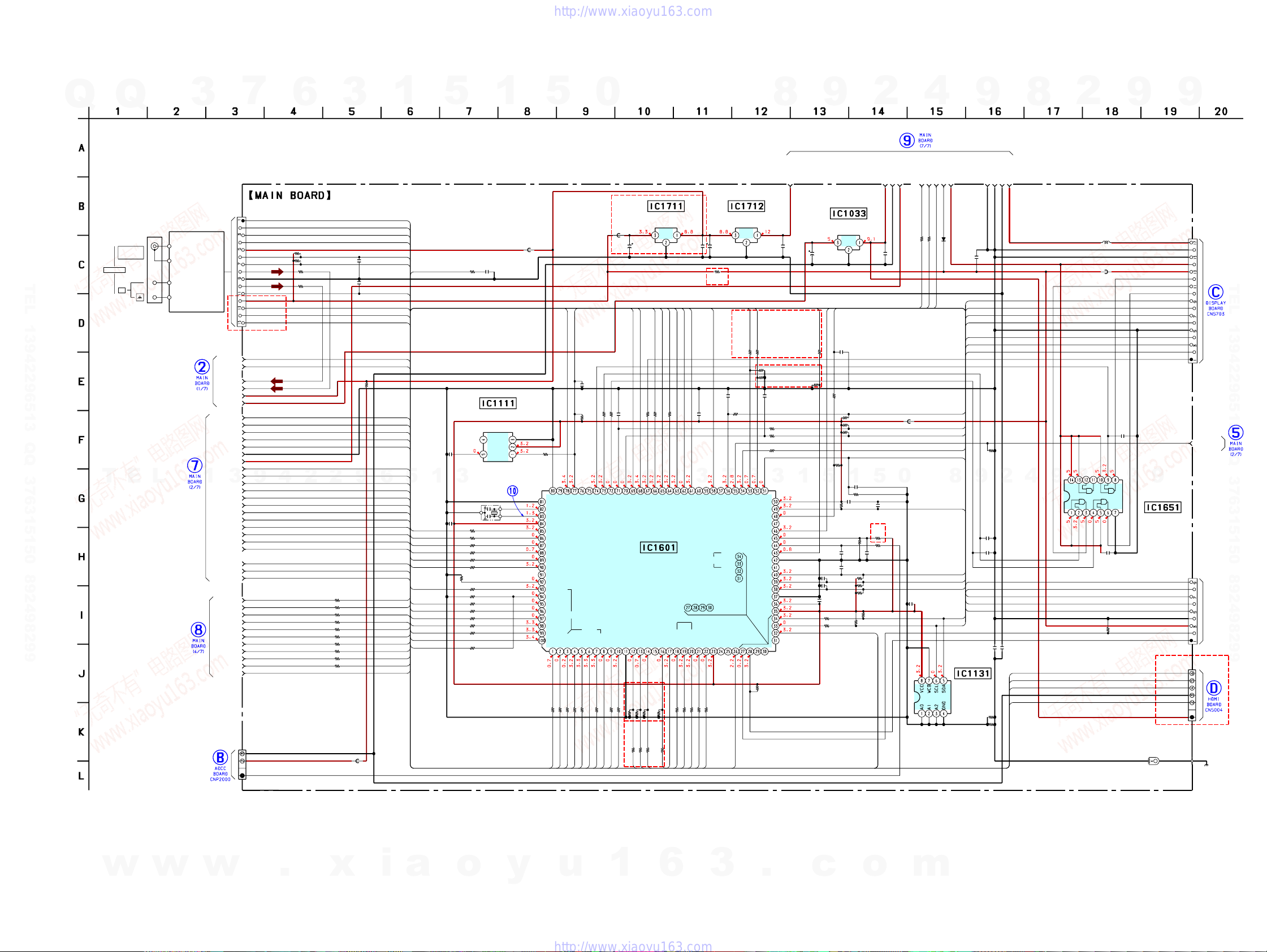
STR-KS1000
Ver. 1.2
5-13. SCHEMATIC DIAGRAM – MAIN Section (3/7) –
Q
Q
3
7
6
• See page 19 for Waveforms. • See page 38 for IC Pin Function Description.
3
1
(3/7)
CLOCK
DO/ST
DI
CE
TUNER_R
TUNER_L
DIR_CLK
DIR_HCE
DIR_XSTAE
DSP_XRST
DSP_ACK
DSP_HDIN
DSP_HCLK
DSP_HCS
DSP_GP12
DSP_GP9
DSP_PM
DSP_BST
~~~~~~~~~~~~~~~~~
DIR_DO
DIR_D1
AD_RST
D-GND
D3.3V
RESET
IO_B
IO_A
3
OVF2
OVF1
LAT3
LAT2
LAT1
SHIFT
SCDT
INIT
~~~~~~~
+9V
TUNED
ST
L CH
GND
R CH
N.C
RDS(3.3V)
FM SIG OUT
RDS_CL
RDS DATA
(AEP,UK)
CNS195
11P(E51,SP,MY,AR)
15P(AEP,UK)
9V
A5V
9
SD~~~
CNP196
3P
AGND
9V
ADCC2
4
R1251
R1252
R1260
R1261
2
39k
39k
0
0
JR1203
0
2
9
R1184
100
R1170
100
R1183
100
R1166
100
R1185
100
R1187
100
R1188
100
R1171
100
R1172
100
R1173
100
FB1314
FM 75Ω
COAXIAL
ANTENNA
TEL 13942296513 QQ 376315150 892498299
AM
TUNER
(Page 23)
DIR_XMODE
T
E
L
1
DIR_DATA0
(Page 24)
DSP_HDOUT
DIR_ERROR
DIR_CKSEL1
(Page 26)
SOFT MUTE
TCLK
TDO
TDA
LAT
TUNED
C1252
0.1
C1251
0.1
T_MUTE
FMSO
RCL
RDATA
IO_B
IO_A
DIR_XMODE
DIR_CLK
DIR_DO
DIR_HCE
DIR_D1
DIR_XSTAE
DSP_XRST
DIR_DATA0
6
DSP_ACK
DSP_HDIN
DSP_HCLK
DSP_HDOUT
DSP_HCS
DSP_GP12
DSP_GP9
DSP_PM
DIR_ERROR
DSP_BST
AD_RST
DIR_CKSEL1
OVFW
OVF
RESET
LAT3
LAT2
LAT1
SHIFT
SCDT
SMUTE
INT
(Page 18)
5
1
5
0
8
9
2
4
9
8
2
9
9
(Page 29)
V
T
NT2
O
-DE
FB1101
C1139
k
1
1
2
2
1
R
T2
ON
P.C
0(AEP,UK)
2.2k(E51)
4.7k(SP,MY)
47k(AR)
0.1
V
CONT1
PC
P
AC
D.DCON5
E4
7
-1
E
T
W
5
5
3
S
k
S
1
1
0
6
2
0
2
0
1
1
R
D
T1
-DET
P.CON
AC
POW SW
2A
2B
SIRCS
MD2
8
MD0
*R1165
AD2
AD1
AD0
SDA
SCL
BR24L16FJ-WE2
GND
V
12V
(AEP,UK)
+9V REGULATOR+3.3V REGULATOR
IC1711
C1732
47
16V
VF
T3
O
LA
3
B
T
L
A
O
L
V
SYSTEM CONTROLLER
1
W
S
IM
S
D
S
H
V
k
k
0
0
1
1
1
2
8
8
0
0
1
1
R
R
0
0
0
0
1
1
8
9
7
7
0
0
1
1
R
R
1
ET
SW
D
(EXCEPT E51,AR)
0
0
1
3
5
0
1
R
Q
F
V
O
MB90488BPF-G
T
E
D
I-
M
D
H
(E51,AR)
k
0
1
3
8
0
1
R
0
0
1
9
8
0
1
R
OEB
TA7809LS
C1731
0.1
T
T
ED
UTE
IN
CD
LAT1
S
M
HIFT
S
TUN
k
1
9
1
1
1
R
S
0
0
1
9
6
1
1
C1138
R
0.1
3
EINT
E
T
T
1
D
D
T
T
E
E
A
N
L
L
U
R
T
E
N
U
T
IC1601
-181E1
B
L
E
E
T
R
O
IP
I-C
I-
M
M
M
D
D
D
H
H
H
k
0
1
4
8
0
1
R
0
0
1
2
9
0
1
R
CLT
S
D
IF
U
C
H
U
S
M
S
O
_
N
T
F
O
S
EEPROM
POWER_RST
1
2
E
S
H
H
S
S
U
A
A
O
L
L
N
F
F
DSP
B
2
_
T
T
T
C
N
U
K
E
O
IN
O
L
L
C
D
D
E
-C
H
H
S
H
P
0
0
0
0
0
0
0
0
100
1
1
1
1
0
7
1
2
6
8
6
6
1
0
1
1
1
1
1
1
R
R1076
R
R
R
T
U
IN
LK
DO
T2
N
_HC
_HD
P_H
_A
SP
SP
IO_B
D
DS
IO
D
P.CO
FB1315
FB1313
ST
V-CONTROL
C1137
0.01
5
1
C1299
0.1
TCLK
TDA
LAT
TDO
T_MUTE
ST
DIR_XMODE
DIR_CLK
DIR_HCE
SD
DIR_D1
DIR_DO
DIR_ERROR
DIR_XSTAE
DIR_CKSEL1
3
X1101
24MHz
R1049
R1042 100
C1163R1163
0.14.7k
RESET SIGNAL GENERATOR
IC1111
S-80929CNM
R1167
100
R1168
100
R1125
1k
R1126
1k
R1115
100
R1116
100
10k
R1041
100
R1043
10k
R1140
100
R1134
100
R1135
100
R1136
100
R1137
100
T
ESE
OVFW
R
C1107
0.1
0
0
0
0
1
1
2
3
2
2
1
1
R1189
1
1
10k
G
V
ONCCD
R1127
100
C1130
R
R
0.01
Q
E
E
S
A
S
V
X0
X1
VCC3
T.CLK
T.DATA
SLATCH
T_DO
T_MUTE
ST
NO USE
LRCK_SW
XMODE
CKSEL1
CLK
CE
DI
DO
E
T
A
T
S
X
0
0
1
4
4
0
1
R
0
ATA
IR_D
D
ERROR
A
0
1
X
X
O
9
A
P
T
G
A
D
0
0
1
2
4
1
1
R
P9
_G
SP
D
B
K
X
W
S
T
F
S
V
U
R
O
O
N
DIR
DSP
N
C
S
T
A
C
S
H
H
B
0
0
0
0
0
0
1
1
1
4
3
9
4
4
4
1
1
1
1
1
1
R
R
R
CK
_HCS
_A
_BST
P
SP
D
DS
DSP
A
IN
S
T
L
L
D
S
C
O
U
_
_
_
V
L
O
L
L
F
F
F
N
A
T
D
S
_
T
R
2
M
S
_
1
P
M
R
D
W
P
X
A
G
P
0
0
0
0
0
0
1
1
1
0
1
1
5
2
5
1
1
1
1
1
1
R
R
R
L
T
O
P12
RS
TR
ST
_PM
_X
R
ON
P_G
SP
SP
AD_
D
DS
D
V-C
IC1712
TA7809LS
OGIOGI
C1728
47
16V
JR1202
(E51,SP,MY,AR)
0
LAT2
7
E
E
2
Y
T
S
S
E
A
K
U
U
L
R
O
O
E
N
N
W
O
P
SDA
SCL
NO USE
E
S
U
O
N
A
_
E
E
T
S
S
C
5
E
U
U
C
L
O
O
C
E
V
S
N
N
C1729
0.1
L
A
(AEP,UK)
RC
AT
D
R
(E51,SP,MY,AR)
10k
R1093
10k
R1094
R1095
C1129
R1129
100
D
S
0.01
10k
R1186
R1105
10k
R1124
100
1
3
6
T
MD2
K
A
S
S
S
L
T
C
D
D
IN
MD1
C
A
R
R
_
IR
D
C
S
MD0
C
D
STOP P.
A
STOP
FUSE
DETECT
P.CONT1
VERSION
ADCC2
RDS
SIGNAL
VSS
NO USE
A/D2
A/D1
A/D0
AVSS
AVRH
AVCC
D
S
_
R
E
W
O
P
R1086
10k
+5V REGULATOR
TA7805LS
C1750 C1751
47
16V
T
SO
T1
FM
C-DE
A
.CON
P
C1108
0.1
R1175R1058R1059
100220220
10k
5
C1142
0.1
C1123
C1124
R1156
R1157
R1128C1102
1000.1
k
0
1
0
9
1
1
R
(E51,SP,MY,AR)
IC1033
OI
G
1
R1635
C1125
0.1
0.1
0.1
0
0
R1088
R1179
R1180
C1105
R1636
C1104
2.2k
R1165 R1164
*
R1158
RESET
M
8
3.3V
0.1
10k
10k
10k
0
5
0.1
2.2k
0.1
C1620
0.1
47k
R1145
100
C1121C1122
0.10.1
10k
R1073
10k
R1072
10k
R1071
R1159
3.3k
3.3k
EEPROM
IC1131
2A
2B
POW SW
SIRCS
AD2
AD1
AD0
SDA
SCL
MD2
MD0
RESET
9
C1152
C1151
0
903
D
_EB
ND
N
D
N
DG
A-G
6V
G
CNS193
17P
+3.3V(STBY)
VOL_JOG(2A)
VOL_JOG(2B)
9
LEVEL SHIFT
IC1651
TC74VHCT08AFT
EB905
POWER SW
TUNER LED
HDMI-CTL
HDMI-DET
HDMI-OEB
HDMI-SW1
FLASH2
FLASH1
FL_LAT
FL_CLK
FL_DIN
CNS192
RESET
CNP195
SIRCS
+7V
+6.0V
9P
6P
GND
GND
+5V
GND
AD2
AD1
AD0
SDA
SCL
MD2
MD0
GND
VDD
GND
TEL 13942296513 QQ 376315150 892498299
(Page 33)
ADCC_INT
(Page 24)
(NC)
(EXCEPT E51)
(Page 31)
(CHASSIS)
10µH
L1600
C1037
0.1
R1100
100k
8
9
4
2
C1066
220p
C1065
220p
C1153
0.1
0.1
CLT
DET
OEB
SW1
C1150
0
C
C
V
2
C1068
0.1
FB1102
R1097
C1067
220p
9
D
N
G
100k
STR-KS1000
w
w
w
.
x
i
a
o
y
u
1
6
2525
3
.
c
o
m
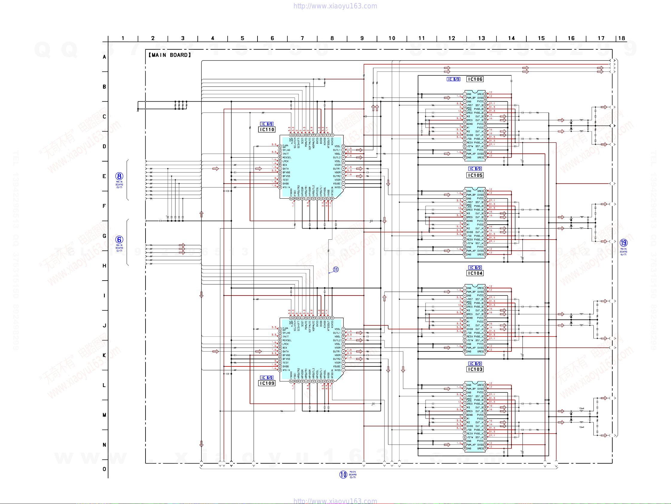
STR-KS1000
5-14. SCHEMATIC DIAGRAM – MAIN Section (4/7) –
Q
Q
3
7
(CHASSIS)
EB907
EB910
6
R468
000
R469
3
R470
R471
0
TEL 13942296513 QQ 376315150 892498299
OVF2
T
E
w
L
w
(Page
25)
1
3
(Page
24)
w
SOFT MUTE
~~~~~~~~~~~~~~~~~
RESET
D-GND
9
LRCKO
OVF1
SD~~~
LAT3
LAT2
LAT1
SHIFT
SCDT
~~~~~~~
INIT
D1
D2
D3
BCKO
SCK
4
.
100
R309
100
R308
100
R306
100
R305
100
R304
100
R303
100
R302
100
R351
100
R300
V
0
5
.1
0
0
2
1
C
C406
0.0047
100
R310
100
R311
100
R312
0
R313
2
100
R314
0
R315
SOFT MUTE
1
p
p
p
0
0
0
0
.0
0
0
0
0
1
1
1
5
4
3
2
0
0
0
0
4
4
4
4
C
C
C
C
2
9
x
(4/7)
RESET
SHIFT
DATA1
DATA2
DATA3
1
NSP MUTE
SOFT MUTE
PGMUTE
SCDT
SHIFT
LAT3
OVF2
INIT
LRCK
OVF2
BCK
OVF
DATA3
SD
LAT3
LAT2
LAT1
SCK
SCDT
INIT
BCK
6
LRCK
SCK
NSP MUTE
SOFT MUTE
PGMUTE
SCDT
SHIFT
LAT2
INIT
LRCK
BCK
DATA2
SCK
2
i
A
5
3
a
A
• See page 19 for Waveforms. • See page 34 for IC Block Diagrams.
5
R319
10k
R353
100
C327
0.1
R326
0
R356
33
C328
0.1
1
3
R354
100
C318
0.1
R327
0
R357
33
C319
0.1
5
4
o
A
A
1
R317
470
STREAM PROCESSOR
R316
470
R318
470
R344
470
STREAM PROCESSOR
6
A
y
5
R328 C320 C322
0 0.1 0.1
C317 C316
0.1 0.1
u
0
R345
R347
10k
10k
C325C326
0.10.1
IC110
CXD9876R
C321
0.1
R329
0
Q
IC109
CXD9876R
C311
0.1
1
R480
0
C324
0.1
R380
C323
R379
C335
16V
Q
C313C312R324 C332
0.10.10 47 16V
6
3
R378
C315
R377
R376
C314
R375
7
A
47
R383R384
560560
R382
560
R381
560
560
0.1
560
7
560
0.1
560
560
0.1
560
3
P6SMB39AT3
P6SMB39AT3
P6SMB39AT3
P6SMB39AT3 1
9
2
D206
D106
D205
D105 L125
8
9
C292
L136
10µH
L126
10µH
0.0022
C266
C226
0.0022
1
R226
2.7
R216
2.7
C256
C216
0.0022
1
C291
0.0022
9
B1
B2
B3
B4
B5
B6
B7
TEL 13942296513 QQ 376315150 892498299
B9
B10
C290
0.0022
C225
C215
2
C265
1
0.0022
R225
2.7
R215
2.7
C255
0.0022
C289
0.0022
B11
9
9
(Page
L135
10µH
10µH
4
IC106
C106
IC105
0
C105
9
C116
1
C186
0.033
C272
0.22
C271 C166 R196
0.22 0.22 3.3
C156
0.033
C196
2200
1
35V
C185
0.033
C210 C175 R205
0.22 0.22 3.3
C209 C165 R195
0.22 0.22 3.3
C155
0.033
9
8
C195
2200
1
35V
C176 R206
0.22 3.3
2
8
C115
1
4
1
2
DIGITAL POWER AMP
CXD9775M
DIGITAL POWER AMP
CXD9775M
5
8
T
D
E
S
S
E
R
3
6
9
R119
22k
R176
0
0.1
C200
0
R166
C146
0.1
R156
0
R146
R246
C136
R117
22k
C145
0.1
R245
C135
0.1
1
0
100
0.1
R136
0
22k
R118
R175
0
0.1
C199
R165
0
R155
0
R145
0
100
R135
0
22k
R116
5
28)
DIGITAL POWER AMP
IC104
DIGITAL POWER AMP
o
CXD9775M
IC103
CXD9775M
C104
C103
m
C184
0.033
C208 C174 R204
0.22 0.22 3.3
C207 C164 R194
0.22 0.22 3.3
C154
0.033
C194
2200
1
35V
C183
0.033
C206 C173 R203
0.22 0.22 3.3
C153
0.033
C193
2200
1
35V
C114
1
C113
1
R193C163C205
3.30.220.22
2
1
A
D204 L134
P6SMB39AT3
D104
P6SMB39AT3
D203
P6SMB39AT3
D103
P6SMB39AT3
4
1
A
C224
1
10µH
L124
C214
10µH
1
L133
C223
1
L123
C213
1
B12
C288
0.0022
C264
0.0022
R224
2.7
R214
2.7
C254
0.0022
C287
0.0022
B13
B14
B15
C286
0.0022
C263
0.0022
R223
2.7
R213
2.7
C253
0.0022
C285
0.0022
B16
R115
22k
R174
0
C198
0.1
R164
100
100
R154
R144
R134
R114
R173
C190
R163
R153
R143
R133
R112
c
0
0
0
0
22k
0
0.1
0
0
0
0
22k
C144
0.1
R244
C134
0.1
R113
22k
C143
0.1
R243
C133
0.1
1
9
8
.
1
A
A
A
STR-KS1000
(Page 27)
2626
 Loading...