

Sony STR-K740P,STR-K840P Service Manual
STR-K740P/K840P
US Model
Canadian Model
AEP Model
UK Model
E Model
SERVICE MANUAL
FM STEREO FM-AM RECEIVER
— Continued on next page —
SPECIFICATIONS
Ver 1.0 2002. 02
Dolby Laboratories Licensing Corporation.
“DOLBY” the double-D symbol ; “AC-3” and “PRO LOGIC”
are trademarks of Dolby Laboratories Licensing Corporation.
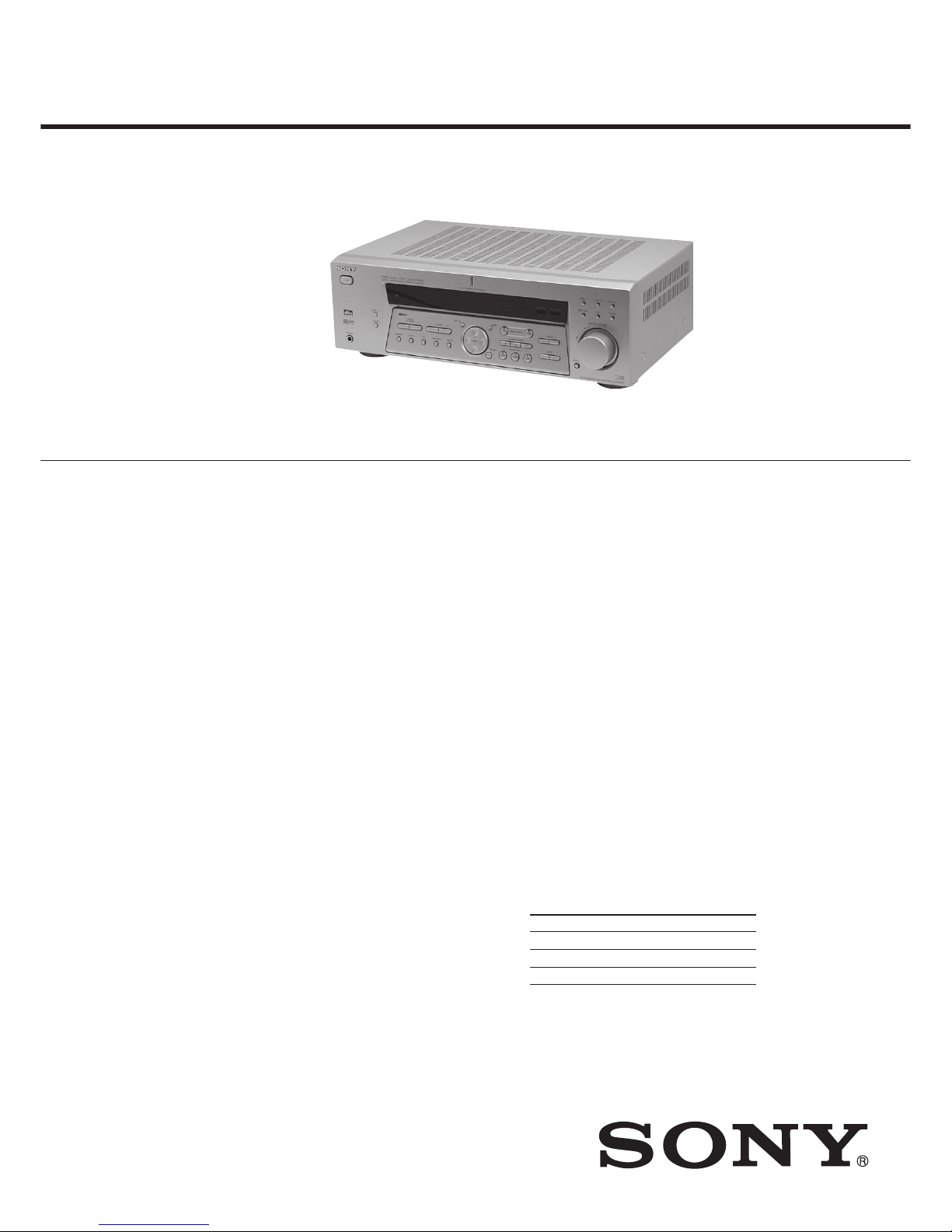
Photo : STR-K840P (SILVER model)
Sony Corporation
Home Audio Company
Published by Sony Engineering Corporation
9-873-544-01
2002B1600-1
© 2002.02
POWER OUTPUT AND TOTAL
HARMONIC DISTORTION:
With 8 ohm loads, both channels driven, from
40 – 20,000 Hz; rated 100 watts (STR-K840P
only)/80 watts (STR-K740P only) per channel
minimum RMS power, with no more than
0.09 % total harmonic distortion from 250
milliwatts to rated output (Models of area code
U only).
Amplifier section
POWER OUTPUT
Models of area code U, CA
Rated Power Output at Stereo Mode
(8 ohms 40 Hz – 20 kHz, THD 0.09 %)
STR-K840P: 100 W + 100 W
STR-K740P: 80 W + 80 W
Reference Power Output
(8 ohms 1 kHz, THD 0.7 %)
STR-K840P: FRONT
1)
:100 W/ch
CENTER
1)
: 100 W
SURR
1)
: 100 W/ch
STR-K740P: FRONT
1)
: 80 W/ch
CENTER
1)
: 80 W
SURR
1)
: 80 W/ch
Models of area code CEL,CEK
Rated Power Output at Stereo Mode
(8 ohms 1 kHz, THD 0.7 %)
STR-K840P: 100 W + 100 W
2)
STR-K740P: 80 W + 80 W
2)
Reference Power Output
2)
(8 ohms 1 kHz, THD 0.7 %)
STR-K840P: FRONT
1)
: 100 W/ch
CENTER
1)
: 100 W
SURR
1)
: 100 W/ch
STR-K740P: FRONT
1)
: 80 W/ch
CENTER
1)
: 80 W
SURR
1)
: 80 W/ch
Models of area code AR, SP
Rated Power Output at Stereo Mode
(8 ohms 1 kHz, THD 0.7 %)
STR-K840P: 90 W + 90 W
Reference Power Output
2)
(8 ohms 1 kHz, THD 10 %)
STR-K840P: FRONT
1)
: 120 W/ch
CENTER
1)
: 120 W
SURR
1)
: 120 W/ch
Models of other area code
Rated Power Output at Stereo Mode
(8 ohms 1 kHz, THD 0.7 %)
STR-K840P: 100 W + 100 W
2)
STR-K740P: 80 W + 80 W
2)
Reference Power Output
2)
(8 ohms 1 kHz, THD 10 %)
STR-K840P: FRONT
1)
: 120 W/ch
CENTER
1)
: 120 W
SURR
1)
: 120 W/ch
STR-K740P: FRONT
1)
: 100 W/ch
CENTER
1)
: 100 W
SURR
1)
: 100 W/ch
1) Depending on the sound field settings and the
source, there may be no sound output.
2) Measured under the following conditions:
Area code Power requirements
E 240 V AC, 50 Hz
SP, CEL, CEK, AR 230 V AC, 50 Hz
MX 120 VAC, 60 Hz
• STR-K740P/K840P are the tuner and the
amplifier section in HT-DDW740/DDW840.

2
STR-K740P/K840P
Inputs (Digital)
DVD/LD (Coaxial)
VIDEO 2 (Optical)
Outputs
MD/TAPE (OUT),
VIDEO 1
(AUDIO OUT)
SUB WOOFER
Tone
Gain levels: ±6 dB, 1 dB step
FM tuner section
Tuning range 87.5 - 108.0 MHz
Antenna terminals 75 ohms, unbalanced
Intermediate Frequency
10.7 MHz
Sensitivity
Mono: 18.3 dBf, 2.2 µV/75 ohms
Stereo:
38.3 dBf, 22.5 µV/75 ohms
Usable sensitivity 11.2 dBf, 1 µV/75 ohms
S/N
Mono: 76 dB
Stereo: 70 dB
Harmonic distortion at 1 kHz
Mono: 0.3%
Stereo: 0.5%
Separation 45 dB at 1 kHz
Frequency response 30 Hz – 15 kHz,
+0.5/–2 dB
Selectivity 60 dB at 400 kHz
AM tuner section
Tuning range
Models of area code U, CA
With 10-kHz tuning scale: 530 – 1710 kHz
6)
With 9-kHz tuning scale: 531 – 1710 kHz
6)
Models of area code E, AR, MX
With 10-kHz tuning scale: 530 – 1610 kHz
6)
With 9-kHz tuning scale: 531 – 1602 kHz
6)
Models of area code MY, SP, CEL, CEK
With 9-kHz tuning scale: 531 – 1602 kHz
Antenna Loop antenna
Intermediate Frequency
450 kHz
Usable sensitivity 50 dB/m (at 1,000 kHz or
999 kHz)
S/N 54 dB (at 50 mV/m)
Harmonic distortion 0.5 % (50 mV/m, 400 Hz)
Selectivity
At 9 kHz: 35 dB
At 10 kHz: 40 dB
6) You can change the AM tuning scale to 9 kHz or
10 kHz. After tuning in any AM station, turn off
the receiver. Hold down PRESET TUNING + and
press . All preset stations will be erased when
you change the tuning scale. To reset the scale to
10 kHz (or 9 kHz), repeat the procedure.
Video section
Inputs
Video: 1 Vp-p, 75 ohms
Outputs
Video: 1 Vp-p, 75 ohms
Sensitivity: –
Impedance: 75 ohms
S/N: 100 dB
(A, 20 kHz LPF)
Sensitivity: –
Impedance: –
S/N: 100 dB
(A, 20 kHz LPF)
Voltage: 250 mV
Impedance: 10 kilohms
Voltage: 2 V
Impedance: 1 kilohms
General
Power requirements
Area code Power requirements
U, CA, MX 120 V AC, 60 Hz
CEL, CEK 230 V AC, 50/60 Hz
MY, SP, AR 220 – 230 V AC, 50/60 Hz
E 120/220/240 V AC, 50/60 Hz
Power consumption
Area code Power consumption
U, MX STR-K840P: 210 W
STR-K740P: 180 W
CA STR-K840P: 300 VA
STR-K740P: 260 VA
CEL, CEK, MY, SP, STR-K840P: 180 W
E, AR STR-K740P: 155 W
Power consumption (during standby mode)
0.5 W
Dimensions 430 145 298 mm
(16 7/8 5 6/8 11 6/8
inches) including
projecting parts and
controls
Mass (Approx.) 7.0 kg (15 lb 7 oz)
Design and specifications are subject to change
without notice.
Frequency response
MULTI CH IN3), CD,
MD/TAPE, DVD/LD,
VIDEO 1, 2
Inputs (Analog)
MULTI CH IN3), CD,
MD/TAPE, DVD/LD,
VIDEO 1, 2
3) HT-DDW840 only
4) INPUT SHORT (with sound field and tone
bypassed).
5) Weighted network, input level.
10 Hz – 50 kHz
+0.5/–2 dB (with sound
field, and tone bypassed)
Sensitivity: 250 mV
Impedance: 50 kilohms
S/N
4)
: 96 dB
(A, 250 mV
5)
)
• Abbreviation
U : US model.
CA : Canadian model.
CEL : AEP model.
CEK : UK model.
SP : Singapore model. (Malaysia model included.)
MX : Mexican model.
MY : Malaysia model.
AR : Argentine model.
3
STR-K740P/K840P
SAFETY-RELATED COMPONENT WARNING!!
COMPONENTS IDENTIFIED BY MARK 0 OR DOTTED LINE WITH
MARK 0 ON THE SCHEMATIC DIAGRAMS AND IN THE PARTS
LIST ARE CRITICAL TO SAFE OPERATION. REPLACE THESE
COMPONENTS WITH SONY PARTS WHOSE PART NUMBERS
APPEAR AS SHOWN IN THIS MANUAL OR IN SUPPLEMENTS
PUBLISHED BY SONY.
After correcting the original service problem, perform the
following safety checks before releasing the set to the customer:
Check the antenna terminals, metal trim, “metallized” knobs, screws,
and all other exposed metal parts for AC leakage. Check leakage as
described below.
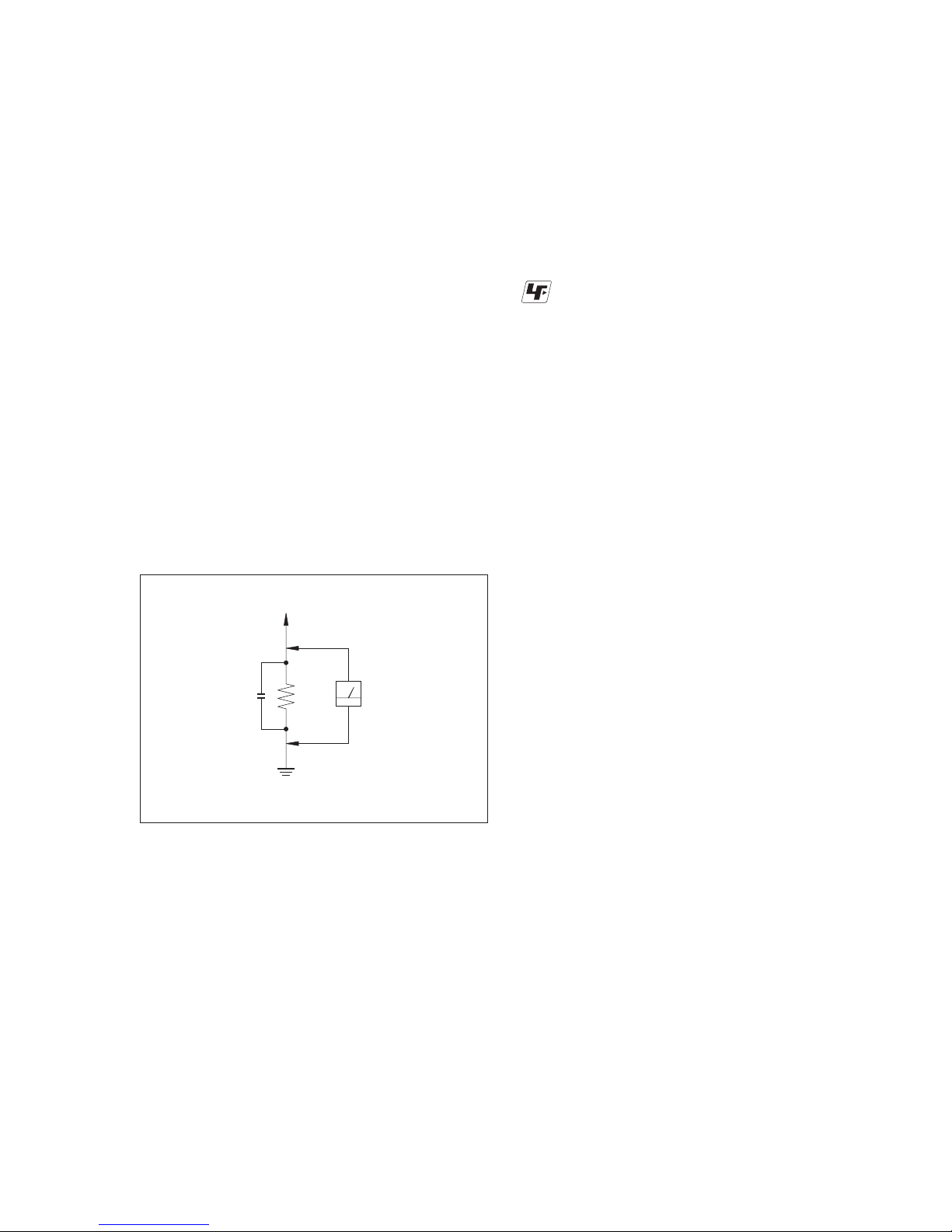
LEAKAGE
The AC leakage from any exposed metal part to earth ground
and from all exposed metal parts to any exposed metal part having
a return to chassis, must not exceed 0.5 mA (500 microamperes).
Leakage current can be measured by any one of three methods.
1. A commercial leakage tester, such as the Simpson 229 or RCA
WT -540A. Follo w the manufactur ers’ instructions to use these
instruments.
2. A battery-operated AC milliammeter. The Data Precision 245
digital multimeter is suitable for this job.
3. Measuring the voltage drop across a resistor by means of a
VOM or battery-operated A C voltmeter . The “limit” indication
is 0.75 V, so analog meter s must ha v e an accurate lo w-v olta ge
scale. The Simpson 250 and Sanwa SH-63Trd ar e examples of
a passive VOM that is suitable. Nearly all battery operated
digital multimeters that have a 2V AC range are suitable. (See
Fig. A)
SAFETY CHECK-OUT
ATTENTION AU COMPOSANT AYANT RAPPORT
À LA SÉCURITÉ!
LES COMPOSANTS IDENTIFÉS PAR UNE MARQUE 0 SUR LES
DIAGRAMMES SCHÉMATIQUES ET LA LISTE DES PIÈCES SONT
CRITIQUES POUR LA SÉCURITÉ DE FONCTIONNEMENT. NE
REMPLACER CES COMPOSANTS QUE PAR DES PIÈSES SONY
DONT LES NUMÉROS SONT DONNÉS DANS CE MANUEL OU
DANS LES SUPPÉMENTS PUBLIÉS PAR SONY.
To Exposed Metal
Parts on Set
0.15 µF
1.5 kΩ
AC
Voltmeter
(0.75 V)
Earth Ground
Fig. A. Using an AC voltmeter to check AC leakage.
Notes on chip component replacement
• Never reuse a disconnected chip component.
• Notice that the minus side of a tantalum capacitor may be
damaged by heat.
Unleaded solder
Boards requiring use of unleaded solder are printed with the leadfree mark (LF) indicating the solder contains no lead.
(Caution: Some printed circuit boards may not come printed with
the lead free mark due to their particular size.)
: LEAD FREE MARK
Unleaded solder has the following characteristics.
• Unleaded solder melts at a temperature about 40°C higher than
ordinary solder.
Ordinary soldering irons can be used but the iron tip has to be
applied to the solder joint for a slightly longer time.
Soldering irons using a temperature regulator should be set to
about 350°C.
Caution: The printed pattern (copper foil) may peel away if the
heated tip is applied for too long, so be careful!
• Strong viscosity
Unleaded solder is more viscous (sticky , less prone to flo w) than
ordinary solder so use caution not to let solder bridges occur such
as on IC pins, etc.
• Usable with ordinary solder
It is best to use only unleaded solder but unleaded solder may
also be added to ordinary solder.
4
STR-K740P/K840P
TABLE OF CONTENTS
1. GENERAL
·········································································· 5
2. TEST MODE ······································································6
3. DIAGRAMS ········································································ 8
3-1. Circuit Board Location ··················································8
3-2. Block Diagrams – MAIN Section – ···························· 10
– DISPLAY/POWER Section –··································· 11
3-3. Printed Wiring Board – DIGITAL Section –··············· 12
3-4. Schematic Diagram – DIGITAL Section (1/2) –·········13
3-5. Schematic Diagram – DIGITAL Section (2/2) –·········14
3-6. Printed Wiring Board – MAIN Section – ···················· 15
3-7. Schematic Diagram – MAIN Section (1/2) – ··············16
3-8. Schematic Diagram – MAIN Section (2/2) – ··············17
3-9. Printed Wiring Board – DISPLAY Section – ··············18
3-10.Schematic Diagram – DISPLAY Section – ················· 19
3-11.Printed Wiring Board – VIDEO Section – ·················· 20
3-12.Schematic Diagram – VIDEO Section – ·····················20
3-13.Printed Wiring Board – POWER Section –················· 21
3-14.Schematic Diagram – POWER Section – ··················· 22
3-15.IC Block Diagrams ······················································ 23
3-16.IC PIN FUNCTION DESCRIPTIONS ······················· 25
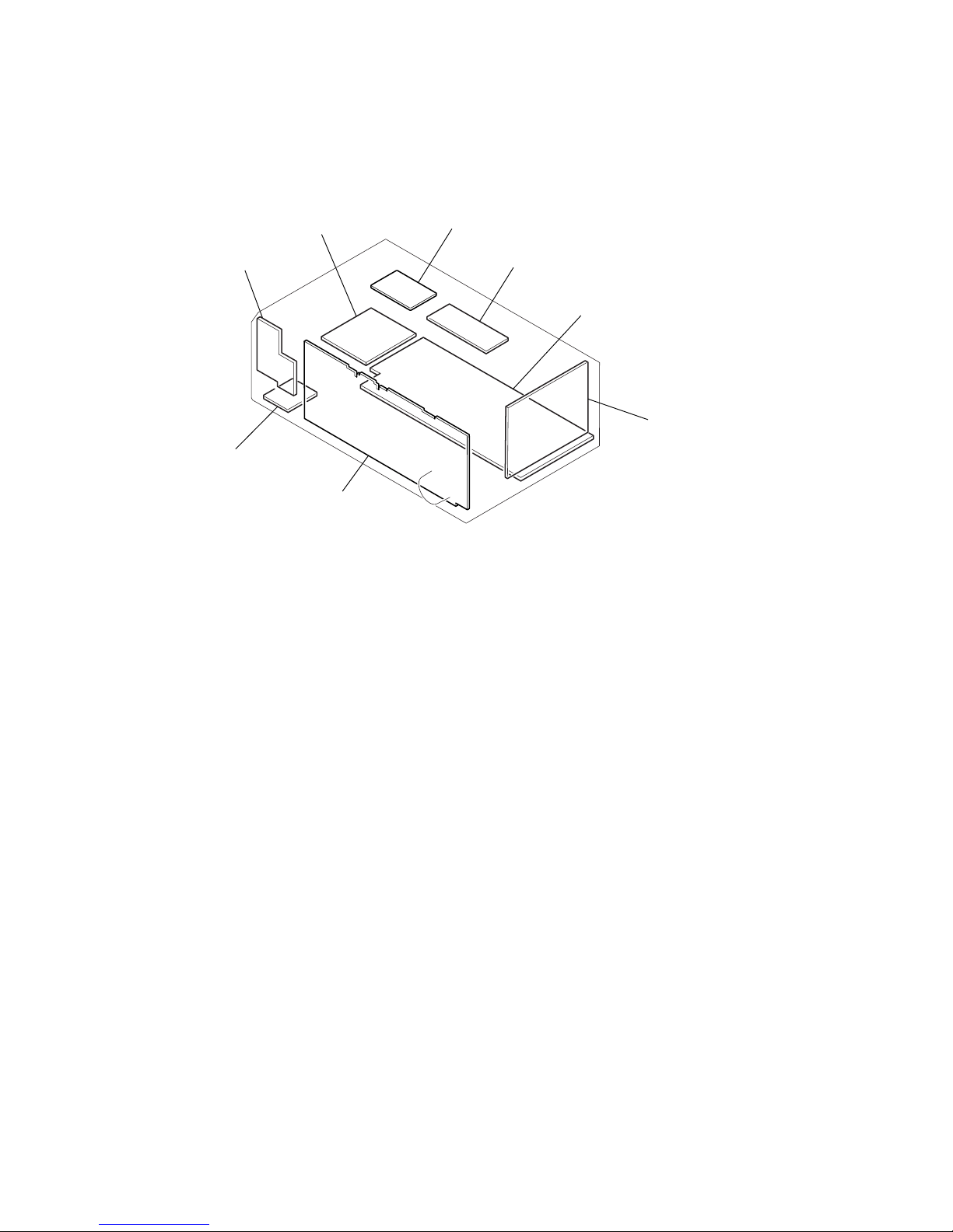
4. EXPLODED VIEWS ······················································ 27
4-1. Front Panel Section ····················································· 27
4-2. Chassis Section-1 ························································ 28
4-3. Chassis Section-2 ························································ 29
5. ELECTRICAL PARTS LIST ·······································30
MODEL IDENTIFICATION
— BACK PANEL —
Parts No.
MODEL PARTS No.
K740P : US 4-238-189-2s
K740P : Canadian 4-238-189-3s
K740P : Malaysia,Singapore 4-238-189-4s
K740P : E 4-238-189-5s
K740P : AEP 4-238-189-6s
K740P : UK 4-238-189-7s
K840P : US 4-238-193-0s
K840P : Canadian 4-238-193-1s
K840P : Malaysia, Singapore 4-238-193-2s
K840P : E 4-238-193-3s
K840P : AEP 4-238-193-4s
K840P : UK 4-238-193-5s
K840P : Argentine 4-238-193-8s
K840P : Mexican 4-238-193-9s
5
STR-K740P/K840P
SECTION 1
GENERAL
This section is extracted
from instruction manual.
g
+
–
1 74 523
6
90qaqsqdqf qg qhqjqkqlw; waws8
FM MODE (Models of area code
CEL, CEK only) ed, (Except for
models of area code CEL, CEK)
ef (32)
INPUT MODE qg (22)
IR (receptor) 4 (39, 46, 52)
LEVEL 0 (16, 20, 28, 57)
M
MASTER VOLUME wd (20, 50)
MD/TAPE qj (22)
MEMORY eh (31, 33)
MENU +/– e; (16, 28, 36, 37, 57)
MENU </> ea (16, 28, 36, 37, 57)
MODE wj (25, 30, 51)
MULTI CHANNEL DECODING
(indicator) (HT-DDW840 only)
7 (22)
MULTI CH IN (HT-DDW840
only) qf (22)
MUTING wf8 (22, 50)
N – S
NAME (36)
PHONES (jack) ek (22, 51)
PRESET/PTY SELECT +/–
(Models of area code CEL, CEK
only) 3 (33, 34)
PRESET TUNING +/– (Except
for models of area code CEL,
CEK) 3 (33, 54)
PTY (models of area code CEL,
CEK only) ef (34)
SET UP 6 (4, 16, 37, 57)
SHIFT eg (33)
SLEEP (HT-DDW740 only) qf
(37)
SURR qd (28, 57)
T – Z
TREBLE +/– qh (30, 57)
TUNER ws (22, 32, 33, 36)
TUNING +/– 5 (32)
VIDEO 1 qk (22)
VIDEO 2 w; (22)
BUTTON DESCRIPTIONS
?/1 (power) 1 (4, 15, 20, 21,
30, 31, 54)
ALPHABETICAL ORDER
0 – 9
2 CH wh (26)
A – D
A.DEC wk (24, 26)
AM (Except for models of area
code CEL, CEK) es (31, 32)
BASS +/– wg (19, 30, 57)
CD ql (22)
CINEMA STUDIO EX A, B, C
9 (25)
Digital Cinema Sound (indicator)
qs (24)
DIMMER ej (23)
DISPLAY 2 (23, 34, 52)
Display qa (23)
DVD/LD wa (22)
E – L
ENTER wl (36)
FM (Except for models of area
code CEL, CEK) ed (31, 32)
FM/AM (Models of area code
CEL, CEK only) es (31, 32)
ek ej eh eg ef ed es ea e; wl wk wj wh wg wf wd
• Abbreviation
CEK : UK model.
CEL : AEP model.
6
STR-K740P/K840P
SECTION 2
TEST MODE
FACTORY PRESET MODE
* All preset contents are reset to the default setting.
* Procedure:
While depressing the VIDEO 1 and the 2CH buttons simultaneously, press the po wer
?/1
button to turn on the main power .
The message “FACTORY” appears and switch off the set.
While depressing the VIDEO 1 and the 2CH buttons simultaneously, press the power
?/1
button again. The message
“FACTORY” appears and the present contents are reset to the
default values.
AM CHANNEL STEP 9 KHZ/10 KHZ
SELECTION MODE
* Either the 9 kHz step or 10 kHz step can be selected for the AM
channel step.
* Procedure:
Set the FUNCTION to AM. Turn off the main power.
While depressing the TUNING+ button or the
PRESET+ button, press the power
?/1
button to turn on the
main power. Either the message “9 k STEP” or “10 k STEP”
appears. Select the desired step.
* For US/Canadian/E model only
SPEAKER SIZE SELECTION MODE
*Either Normal Speaker or Micro Satellite Speaker can be selected.
*Procedure:
While depressing the LEVEL button, press the po wer
?/1
button
to turn the main power.
Either the message “NORM. SP.” or “MICRO SP.” is displayed.
Select the desired speaker size.
FLUORESCENT INDICATOR TUBE TEST MODE
* All fluorescent segments are tested. When this test is activated,
all segments turn on at the same time, then each segment turns on
one after another.
* Procedure:
While depressing the MD/T APE and the SHIFT b uttons simultaneously, press the po wer
?/1
button to turn on the main power .
1. All segments turn on.
MULTI CHANNEL DECODING , Digital Cinema Sound ,
A.F.D. , MODE , 2CH and SET UP LED turn on.
2. Press the VIDEO button, confirm display.
A.F.D. , MODE , LEVEL , SET UP , and Digital Cinema Sound
LED turn on.
3. Press the VIDEO button, confirm display
MULTI CHANNEL DECODING , 2CH , SURR and NAME
LED turn on.
4. Press the VIDEO button, All segments turn off.
5. Every pressing of the VIDEO button turns on each
segment and LED one after another in the same order.
(Not only the VIDEO button, b ut also the other buttons such as
DVD/LD , TV/SAT , MD/TAPE , CD , TUNER and AUX can
be used.)
SOUND FIELD CLEAR MODE
* The preset sound field is cleared when this mode is activated.
Use this mode before returning the product to clients upon
completion of repair.
* Procedure:
While depressing the MODE button, press the power
?/1
button
to turn on the main power.
The message “SURR. CLR.” appears and initialization is
performed.
DEMONSTRATION MODE
* Demonstration is performed.
* Procedure :
While depressing the SET UP button, press the power
?/1
button. The message appears and demonstration is performed.
* To finish DEMONSTRATION MODE, press the power
?/1
button while the introduction message appears in the display.
SOFTWARE VERSION DISPLAY MODE
* The software version is displayed.
* Procedure:
While depressing the ENTER and the A.F.D buttons
simultaneously, press the po wer
?/1
button to turn on the main
power . The model name, destination and the software version are
displayed.
KEY CHECK MODE
* Button check
* Procedure:
While depressing the VIDEO 1 and the SHIFT buttons
simultaneously, press the po wer
?/1
button to turn on the main
power.
“REST 39” appears. (AEP, UK, model: “RESET 38”)
Every pressing of any button other than ?/1 and SPEAKERS
counts down the buttons. The b uttons which are already counted
once are not counted again. When all buttons are pressed “REST
00” appears.
When MASTER VOLUME is rotated in clockwise direction,
“VOL MIN”, “VOL 1” to “VOL 48”, “VOL MAX” appear.
SW
LSLCR
SSR
SLEEP
SP.OFF
( ( ( L F E ) ) )
DIGITAL
OPT COAX MULTI CH IN
PRO LOGIC DTS MPEGSTEREO MONORDS MEMORY
MUTINGINFONEWSTAEQD.RANGE
D
D
dB
kHz
mft.
MHz
SW
LR
S
SLEEP
L F E
COAX
PRO LOGIC MPEGSTEREO RDS
MUTINGINFOTAD.RANGE
D
D
k
m
MHz
SL
C
SR
SP.OFF
( ( ( ) ) )
DIGITAL
OPT MULTI CH IN
DTS MONO MEMORY
NEWSEQ
dB
Hz
ft.

7
STR-K740P/K840P
AUTO BETICAL MODE
* This mode is installed in the Europe models only. When this mode
is used, the receiver scans the broadcasts that can be received by
the tuner, and sets up the broadcasts. Be sure to start scanning
after connecting the antenna.
* Procedure:
1. Check that the antenna is connected.
2. Press the ?/1 button to turn on the power while pressing the
MEMORY button.
3. The message “AUTO-BETICAL SELECT” appears and the
receiver starts scanning.
8
STR-K740P/K840P
SECTION 3
DIAGRAMS
3-1. Circuit Board Location
VIDEO board
DIGITAL board
MAIN board
DISPLAY board
HEADPHONE board
POWER SW board
STANDBY board
AC SELCT board (E model only)
99
STR-K740P/K840P
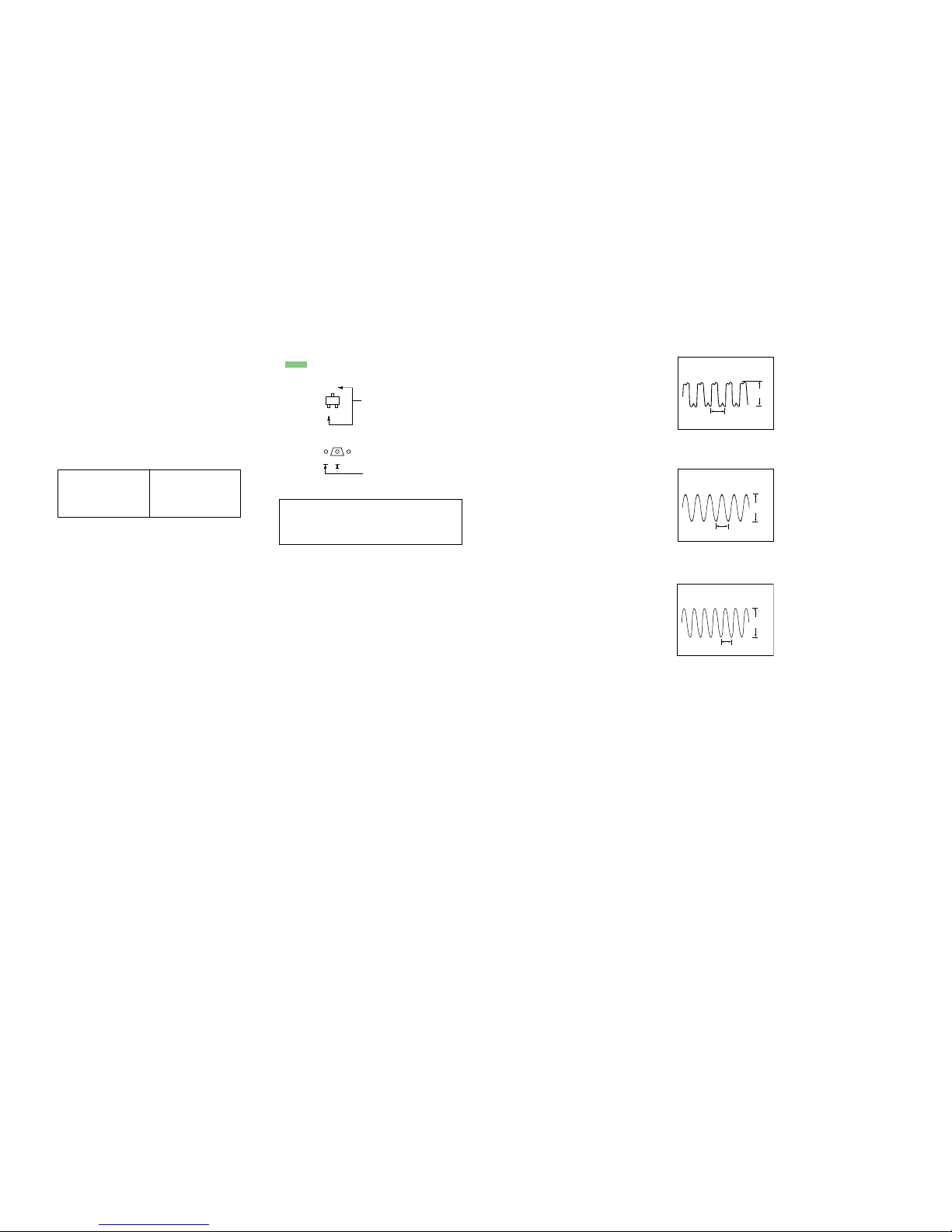
• Waveform
DIGITAL Board
1 IC1101 wa (XOUT)
4.4Vp-p
81ns
(12.288MHz)
2 IC1201 9 (MCLK1)
3.3Vp-p
73ns (13.59MHz)
3 IC1601 id (XI)
2.8Vp-p
5ns (20MHz)
For schematic diagrams.
Note:
• All capacitors are in µF unless otherwise noted. p : pF. 50
WV or less are not indicated except for electrolytics and
tantalums.
• All resistors are in Ω and 1/
4
W or less unless otherwise
specified.
• % : indicates tolerance.
•f: internal component.
• 2 : nonflammable resistor.
• 5 : fusible resistor.
• C : panel designation.
• A : B+ Line.
• B : B– Line.
• Voltages and waveforms are dc with respect to ground
under no-signal (detuned) conditions.
No mark : FM
• Voltages are taken with a VOM (Input impedance 10 MΩ).
Voltage variations may be noted due to normal production tolerances.
• Waveforms are taken with a oscilloscope.
• Circled numbers refer to waveforms.
• Signal path.
F : FM
J : CD (ANALOG)
c : DVD (DIGITAL)
• Abbreviation
CND : Canadian model
MY : Malaysia model
SP : Singapore model
AR : Argentine model
MX : Mexican model
THIS NOTE IS COMMON FOR PRINTED WIRING
BOARDS AND SCHEMATIC DIAGRAMS.
(In addition to this necessary note is printed in each
block.)
Note:
The components identified by
mark 0 or dotted line with mark
0 are critical for safety.
Replace only with part number
specified.
Note:
Les composants identifiés par
une marque 0 sont critiques
pour la sécurité.
Ne les remplacer que par une
pièce portant le numéro spécifié.
Caution:
Pattern face side: Parts on the pattern face side seen from
(Side A) the pattern face are indicated.
Parts face side: Parts on the parts face side seen from
(Side B) the parts face are indicated.
For printed wiring boards.
Note:
• X : parts extracted from the component side.
•
a
: Through hole.
•
f
: internal component.
• : Pattern from the side which enables seeing.
C
B
These are omitted.
E
Q
B
These are omitted.
CE
1010
STR-K740P/K840P
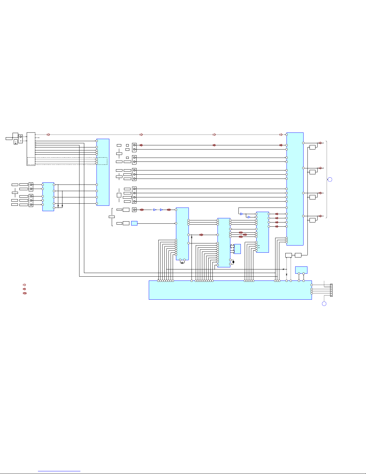
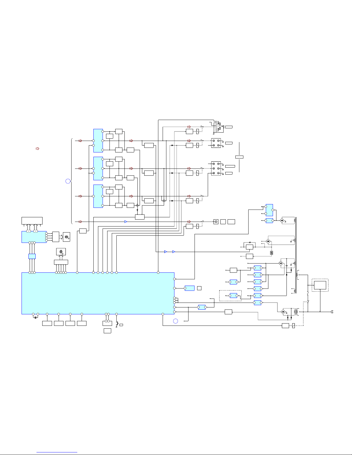
3-2. Block Diagrams – MAIN Section –
AUDIO IN
AUDIO IN
AUDIO IN
MULTI
CH IN
FRONT
SURROUND
CENTER
SUB WOOFER
J401
PROC.
L IN9
2
L REC3
67
L IN7
71
L IN2
63
L REC1
61
L IN1
62
51
L OUT
L IN5
69
47
SL OUT
39
C OUT
35
SW OUT
MUTING
Q361
DATA
20
CLK
21
LATCH
22
MUTING
Q365
MUTING
Q363
MUTING
Q364
15
CLK
SDA
SCL
16
LATCH
14
DATA
SYSTEM CONTROL
IC1601(2/3)
J404
DVD/LD
IN
VIDEO 2
IN
J1101
35
62
IC1102
DIGITAL AUDIO
I/F RECEIVER
IC1101
L
DIN2
5
DO
35
DI
36
CLK
38
CE
37
ERROR
34
XSTATE
17
XMODE
48
13
CK OUT
14
BCK
15
LRCK
16
DATAO
IC1102
X1101
12.288MHz
AUDIO DSP
IC1201
KFSI0
22
SDI2
30
HCLK
34
HCS
36
HACN
32
PM
113
BST
56
XRST
2
23
SDO1
24
SDO2
25
SDO3
BCKI2
29
LRCKI2
28
IC1202
SRAM
AUDIO CODEC
IC1501
MCLKI
39
CDT1
43
CCLK
42
CS
41
PD
17
S.MUTE
3
27
L OUT1
BCK
4
LRCK
5
SDTO
9
SDTI1
6
SDTI2
7
SDTI3
8
25
L OUT2
23
L OUT3
24
R OUT3
LIN+
30
LIN-
29
21
IC1502
67
IC1502
ANALOG SOUND
AL IN
11
SL
13
16
15
AL OUT
10
DL IN
27
29
31
32
ASL IN
ASW IN
AC IN
SL
C
SW
DSL IN
DC IN
DSW IN
A
98 97 95 96 99100 94 1
DO
DI
CLK
CE
ERROR
XSTATE
CKSEL1
DATA0
20
HCLK
4
HCS
5
HACN
7PM3
BST
6
XRST
10
CDT1
12
SCL
13CS8PD9
SMUTE
24
ANA/DIG
MUTING
CONT
Q1601,1602
21
5 6
34 33
F.MUTING
MUTING
SWITCH
Q379
49MD0
51
MD2
28
SP SWITCH/FLASH 1
27
FLASH 2
MD0
VDD
MD2
FLASH 1
FLASH 2
RESET
+3.3V
CNS3
B
J403
J402
CD
MD/TAPE
DVD/LD
VIDEO 2
AUDIO OUT
OPTICAL
IN
IC1105
DIN1
4
• Signal Path
• R-CH is omitted due to same as L-CH.
: FM
: CD(ANALOG)
: DVD (DIGITAL)
22 21
XIN XOUT
93
XMODE
CKSEL1
47
GP9
68
HD OUT
35
HD IN
33
2
GP9
18
HD OUT
19
HD IN
9
MCLK1
12
MCLK2
X1201
13.5MHz
14
SCK OUT
20
BCKO1
19LRCKO
18SDI1
24AUDIO
GP8
69
EXLOCK
59
L IN8
1
FLASH
FOR
PROGRAMMING
TUNER PACK
FM
75 Ω
COAXIAL
AM
R-CH
ST-DI
ST-DO
CLK
CE
STEREO
TUNED
MUTING
FM
AM
R CH
L CH
SYSTEM CONTROL.
IC1601(1/3)
DO
76
J200
V1 OUT
15
V1
13
M.OUT
1
14
SW1
VIDEO SELECT
VIDEO OUT
VIDEO OUT
VIDEO 1
MONITOR
J201
V2
5
DVD
3
DVD/LD
VIDEO 1
VIDEO IN
VIDEO IN
VIDEO IN
VIDEO 2
IC103
10
SW2
4
SW3
6
SW4
2
SW5
SLATCH
78
STEREO
74
TUNED
73
MUTING
75
RDS-DATA
RDS DATA
53
RDS-INT
RDS CLOCK
52
FM SIG OUT
RDS SIGNAL
43
SW1
90
SW2
89
SW3
88
SW4
87
IN
OUT
IN
COAXIAL
OPTICAL
DIGITAL
ANTENNA
AEP, UK
D204
D203
-
-
D1101
IC201
D1601
SDA SCL
EEPROM
IC1604
1111
STR-K740P/K840P
– DISPLAY/POWER Section –
IN2
8
12
+V OUT2
POWER AMP
IC701
POWER AMP
IC702
9
NF2
LIMITER
Q701,702
11
-V OUT2
IN2
12
+V OUT2
9
NF2
11
-V OUT2
BOOSTER
Q703
BOOSTER
Q704
CURRENT
DETECT
Q705,706
AF POWER
PROTECT
Q740
LIMITER
Q651,652
BOOSTER
Q653
BOOSTER
Q654
CURRENT
DETECT
Q655,656
IN+
1
6
+V OUT
POWER AMP
IC501
2
IN-
LIMITER
Q501,502
5-V OUT
BOOSTER
Q503
BOOSTER
Q504
CURRENT
DETECT
Q505,506
D721
PROTECT
SWITCH
Q722,723,725
RELAY
DRIVE
Q790
RY791
RELAY
DRIVE
Q710
RY701
D731
RELAY
DRIVE
Q610
RY601
D733
RELAY
DRIVE
Q550
RY501
D734
IC401
5
7
RELAY
DRIVE
Q560
RY560
L
R
SR
SL
C
R-CH
R-CH
R-CH
PHONES
TM601
TM602
AUDIO
OUT
J405
67
PROTECTOR
68
HEADPHONE RELAY
72
PREOUT/FRONT RELAY
70
REAR RELAY
71
CENTER RELAY
69
WOOFER RELAY
LED DRIVE
Q100-104
RV102
ENCODER
3 1
VOL(B)59VOL(A)
60
POWER KEY
56
?/1
S145
77
RSTX
48
STOP
54
SIRCS
55
FUSE DETECT
REMOTE
CONTROL
RECEIVER
1
IC102
D910-913
AC
IN
T902
RY901
D915
F901
D914
RELAY
DRIVE
Q901
D820-823
23
VCC5
84
VCC3
-5V
REG
3 2
+5V
REG
3 1
-7V
REG
3 2
+7V
REG
1 3
AUDIO
+7V
VIDEO
+5V
VIDEO
-5V
IC801
IC802
IC807
IC804
POWER RELAY
66
RELAY
+B
D902-905
82 83
X0
X1
X1601
20.0MHz
F1
F2
L
SLSL
C
SW
A
MUTING
1
MUTING
1
POWER
MUTING
Q747,748
22
AC MUTING
J791
FLUORESCENT
INDICATOR TUBE
FL101
61
DIN
62
CLK
63
FL_STB
7
DIN8CLK9STB
14 29
SEG1-16
42 31
GRID1-12
F1 F2
1
SW1
2
SW2
3
SW3
4
SW4
FL DRIVE
IC100
D111-114
29
BLUE LED
30
MODE LED
31
2CH LED
32
AFD LED
26
DCS LED
FUNCTION
KEY
A/D0
38
S110-119S100-109
FUNCTION
KEY
A/D1
39
FUNCTION
KEY
A/D2
40
S120-128
FUNCTION
KEY
A/D3
41
S130-137,
S143,144
B
RESET
SYSTEM CONTROL
IC1601(3/3)
• Signal Path
• R-CH is omitted due to same as L-CH
: FM
AF POWER
PROTECT
Q640
AF POWER
PROTECT
Q540
IC601
21
FRONT
SURROUND
CENTER
IC601
57
25
HP DETECT
BUFFER
IC101
D100-104
35
AVCC
+3.3V
REG
3 1
IC1904
AUDIO
-7V
D899
D898
+10V
REG
3 1
TUNER
+10V
IC1902
T901
+3.3V REG
Q471
Q921
AC DET
+3.3V
REG
3 1
IC1905
1 2
IC1602
TUNER
+3.3V
+3.3V
D802
+B
-B
-B SW
Q691,692
-30V REG
Q801
FL101
-30V
POWER AMP
-B
+5V
REG
3 1
IC1903
+5V
+2.5V
REG
5
+2.5V
+3.3V
REG
2
4
IC1901
+3.3V
+5V
REG
3 1
IC1503
AUDIO
+5V
SPEAKERS
SUB
WOOFER
MASTER
VOLUME
8
Q107-111
LED
DRIVE
RESET
+3.3V(STBY)
K740P:AEP,UK
K840P:AEP,UK
S901
VOLTAGE
SELECTOR
K740P:E/K840P:E MODEL ONLY
g
1212
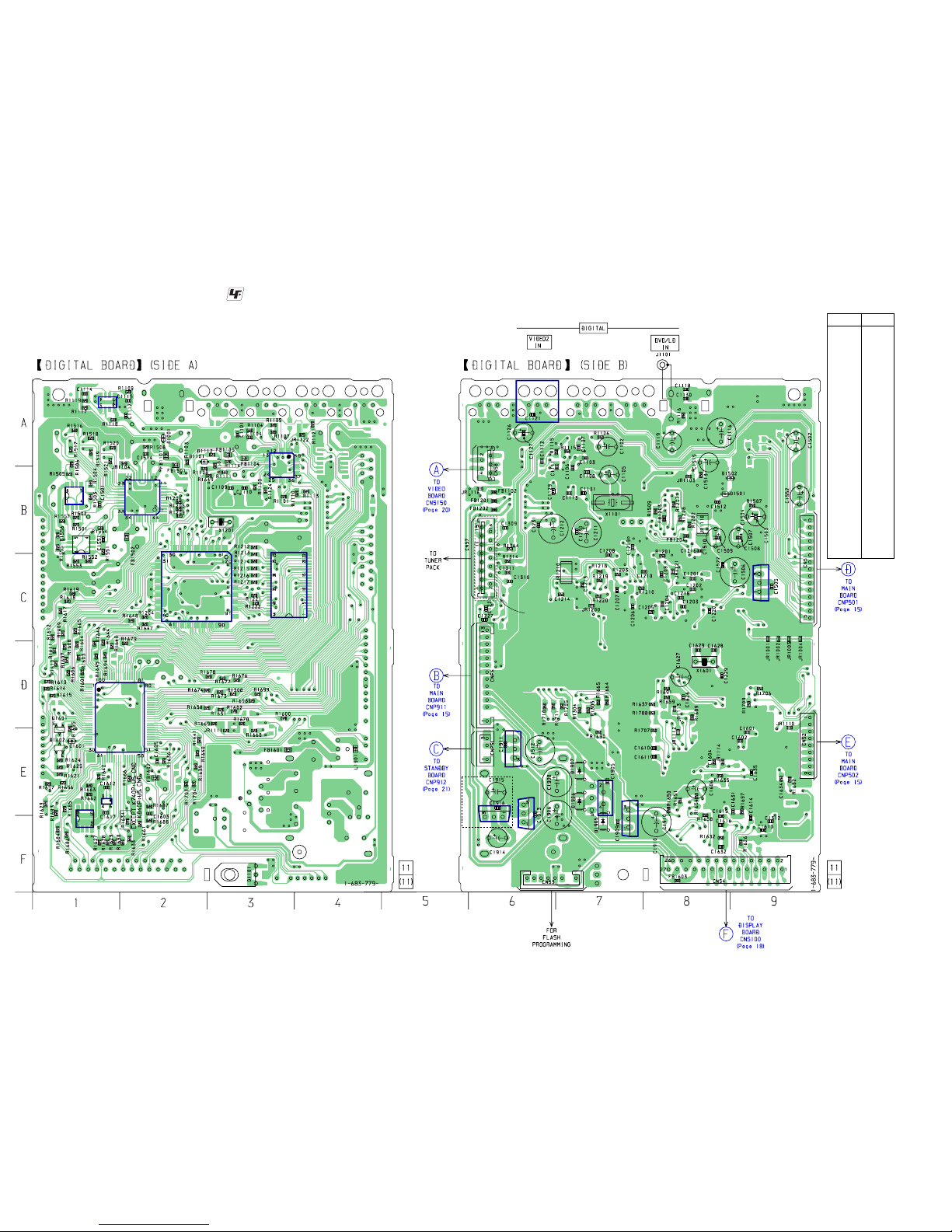
STR-K740P/K840P
• See page 8 for Circuit Boards Location.
3-3. Printed Wiring Board – DIGITAL Section –
IC1102
IC1502
IC1501
IC1101
IC1552
IC1201
IC1202
IC1601
IC1604
IC1602
IC1105
IC1503
IC1904
IC1902
IC1905
IC1901
IC1903
11P:EXCEPT K740P:AEP,UK/K840P:AEP,UK
15P:K740P:AEP,UK/K840P:AEP,UK
K740P:AEP,UK/K840P:AEP,UK
• : Uses unleaded solder.
Ref. No. Location
D1001 A-2
D1101 A-3
D1501 B-8
D1502 B-8
D1601 E-1
D1905 F-7
D1906 E-7
D1907 E-7
IC1101 A-3
IC1102 A-1
IC1105 A-6
IC1201 C-2
IC1202 C-3
IC1501 B-2
IC1502 B-1
IC1503 C-9
IC1552 B-1
IC1601 D-1
IC1602 E-1
IC1604 F-1
IC1901 E-7
IC1902 E-6
IC1903 F-7
IC1904 E-6
Q1601 D-1
Q1602 E-1
• Semiconductor
Location
1313
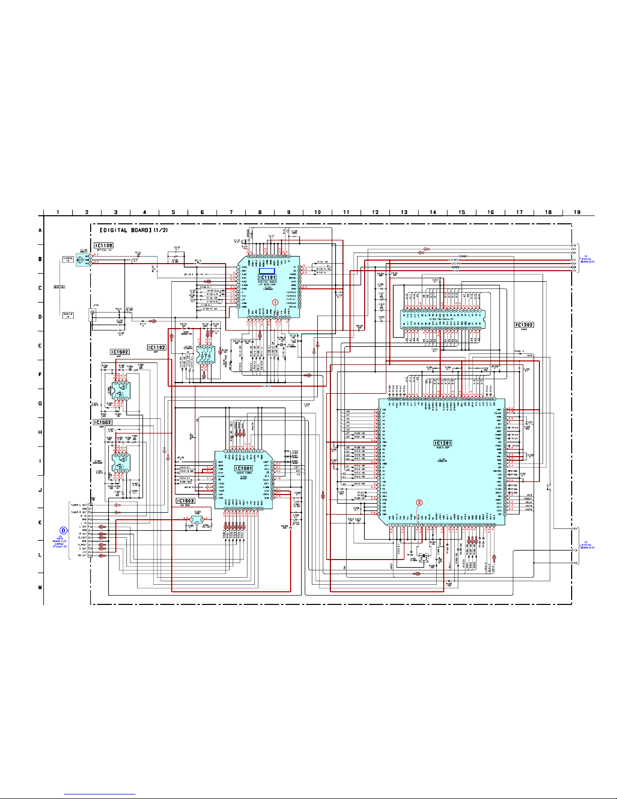
STR-K740P/K840P
3-4. Schematic Diagram – DIGITAL Section (1/2) –
• See page 9 for Waveform. • See page 23 for IC Block Diagrams.
IC B/D
1414
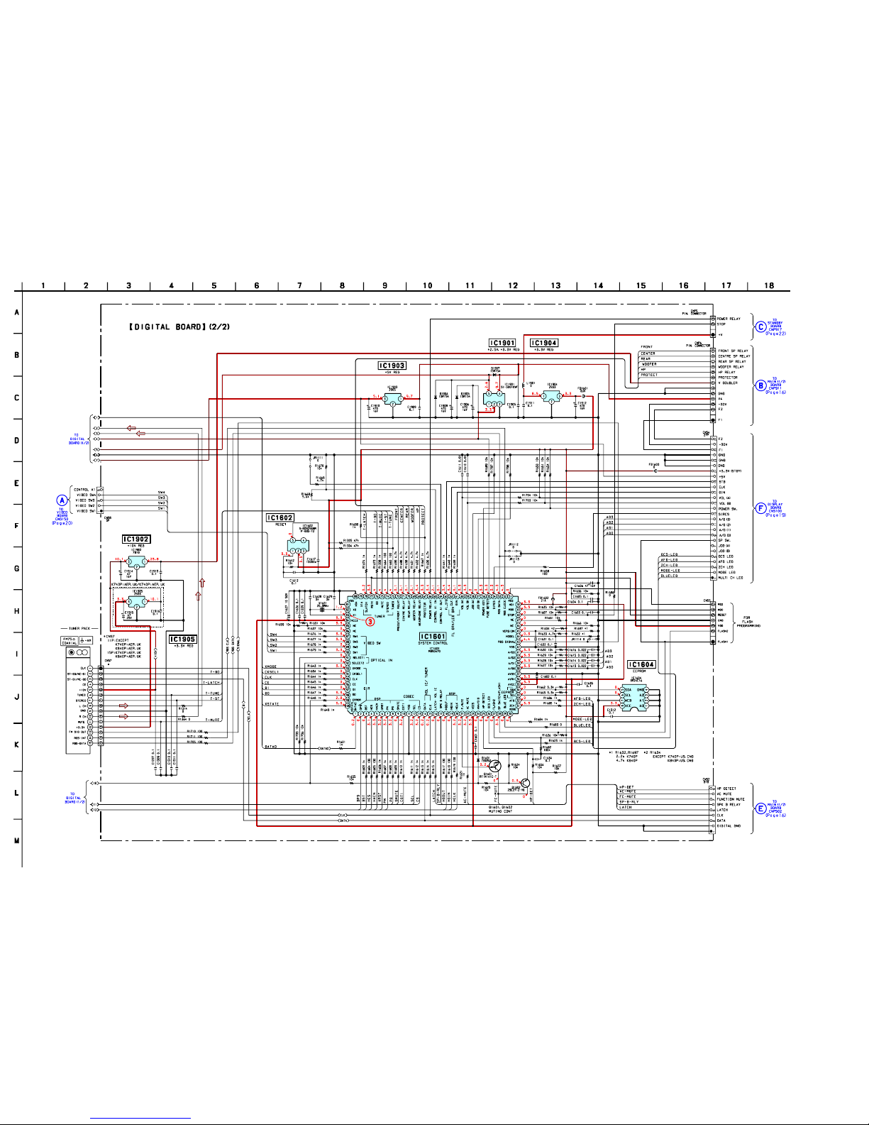
STR-K740P/K840P
3-5. Schematic Diagram – DIGITAL Section (2/2) –
• See page 9 for Waveform. • See page 25 for IC Pin Function Description.
 Loading...