

STR-K7200
SERVICE MANUAL
Ver. 1.0 2008.02
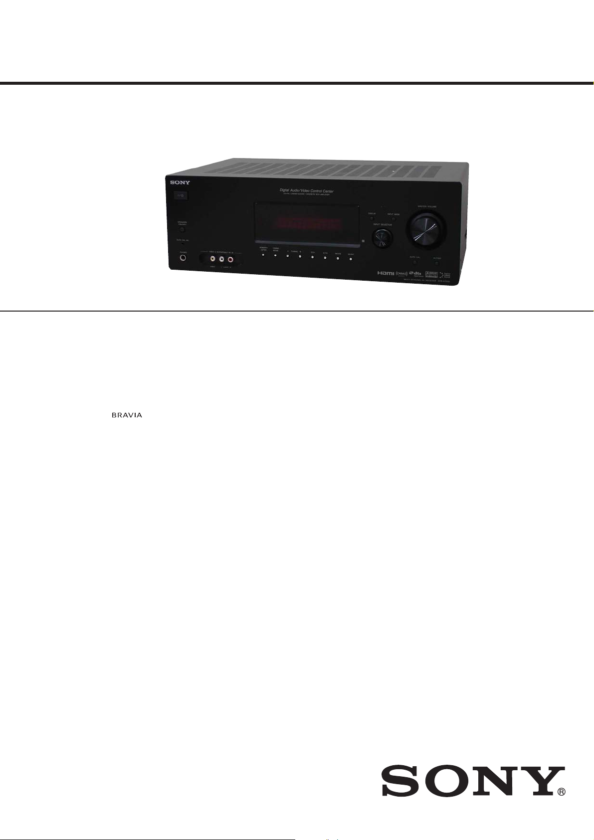
• STR-K7200 is the receiver section in HT-7200DH.
This receiver incorporates Dolby* Digital and Pro Logic Surround and the DTS** Digital Surround System.
* Manufactured under license from Dolby Laboratories. Dolby, Pro Logic, and the double-D symbol are
trademarks of Dolby Laboratories.
** Manufactured under license under U.S. Patent #’s: 5,451,942; 5,956,674; 5,974,380; 5,978,762; 6,487,535
& other U.S. and worldwide patents issued & pending. DTS and DTS Digital Surround are registered
trademarks and the DTS logos and Symbol are trademarks of DTS, Inc. © 1996-2007 DTS, Inc.
All Rights Reserved.
This receiver incorporates High-Definition Multimedia Interface (HDMI
and High-Definition Multimedia Interface are trademarks or registered trademarks of HDMI Licensing LLC.
The XM name and related logo are registered trademarks of XM Satellite Radio Inc. All rights reserved.
“x.v.Color” and “x.v.Color” logo are trademarks of Sony Corporation.
“BRAVIA” and are trademarks of Sony Corporation.
TM) technology.HDMI, the HDMI logo
US Model
AUDIO POWER
SPECIFICATIONS
POWER OUTPUT AND TOTAL
HARMONIC DISTORTION:
With 6 ohm loads, both channels driven, from
120 – 20,000 Hz; rated 90 watts per channel
minimum RMS power, with no more than 1%
total harmonic distortion from 250 milliwatts
to rated output.
Amplifier section
Power Output
Stereo mode (rated)
(6 ohms 1
Surround mode (reference)
(6 ohms 1 kHz
1)
kHz, THD 1%)
90 W + 90 W
, THD 10%)
RMS Output
FRONT: 140 W
per channel
CENTER: 140 W
SURROUND: 140 W
per channel
2)
SPECIFICATIONS
1)
Measured under 120 V AC, 60 Hz
2)
Reference power output for front, center and
surround speakers. Depending on the sound field
settings and the source, there may be no sound
output.
Inputs
Analog
Digital (Coaxial) Impedance: 75 ohms
Outputs (Analog)
AUDIO OUT Voltage: 800 mV/
SUB WOOFER Voltage: 2 V/1 kohm
Tone
Gain levels ±6 dB, 1 dB step
Reproduction frequency range
FM tuner section
Tuning range 87.5 – 108.0 MHz
Antenna FM wire antenna
Antenna terminals 75 ohms, unbalanced
Intermediate frequency
Sensitivity: 800 mV/
50 kohms
10 kohms
28 – 20,000 Hz
10.7 MHz
AM tuner section
Tuning range
With 10-kHz tuning scale:
With 9-kHz tuning scale:
Antenna Loop antenna
Intermediate frequency
3)
You can change the AM tuning scale to 9 kHz or
10 kHz. After tuning in any AM station, turn off
the receiver. While holding down TUNING
MODE, press ?/1. All preset stations will be
erased when you change the tuning scale. To reset
the scale to 10 kHz (or 9 kHz), repeat the
procedure.
Video section
Inputs/Outputs
Video: 1 Vp-p, 75 ohms
COMPONENT VIDEO:
530 – 1,710 kHz
531 – 1,710 kHz
450 kHz
Y: 1 Vp-p, 75 ohms
P
B/CB: 0.7 Vp-p, 75 ohms
P
R/CR: 0.7 Vp-p, 75 ohms
80 MHz HD Pass Through
3)
3)
– Continued on next page –
9-887-947-01
2008B05-1
2008.02
©
MULTI CHANNEL AV RECEIVER
Sony Corporation
Audio Business Gourp
Published by Sony Techno Create Corporation
STR-K7200
General
Power requirements 120 V AC, 60 Hz
Power output (DIGITAL MEDIA PORT)
DC OUT 5 V, 0.7A MAX
Power consumption 170 W
Power consumption (during standby mode)
0.3 W (when “CONTROL
FOR HDMI” in VIDEO
menu is set to “CTRL
OFF”)
Dimensions (w/h/d) (Approx.)
17 × 6 1/4 × 12 5/8 inches
(430 × 157.5 × 318 mm)
including projecting parts
and controls
Mass (Approx.) 17 lb 4 oz (7.8 kg)
Design and specifi cations are subject to
change without notice.
SAFETY CHECK-OUT
After correcting the original service problem, perform the following safety check before releasing the set to the customer:
Check the antenna terminals, metal trim, “metallized” knobs,
screws, and all other exposed metal parts for AC leakage.
Check leakage as described below.
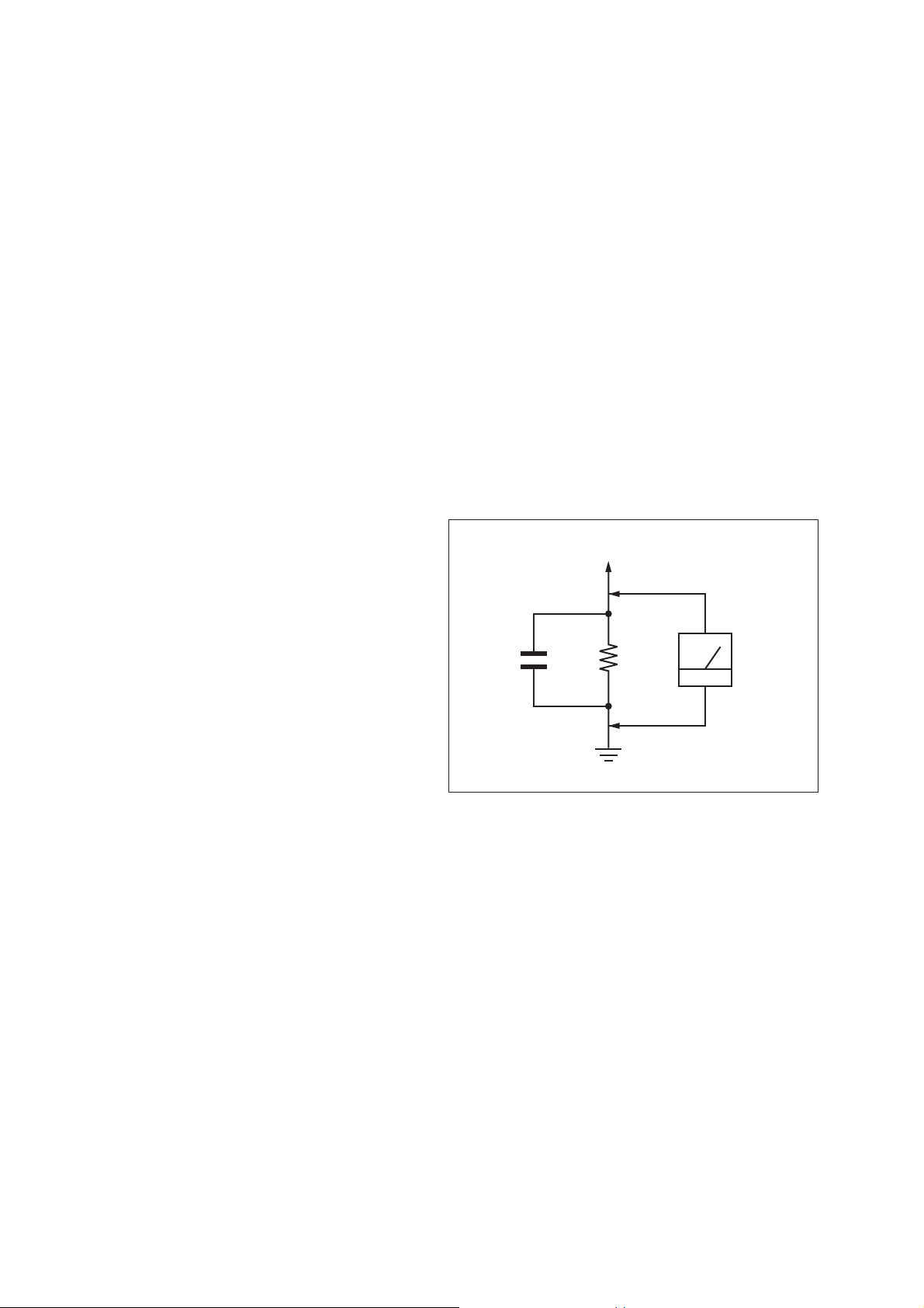
LEAKAGE TEST
The AC leakage from any exposed metal part to earth ground and
from all exposed metal parts to any exposed metal part having a
return to chassis, must not exceed 0.5 mA (500 microamperes.).
Leakage current can be measured by any one of three methods.
1. A commercial leakage tester, such as the Simpson 229 or RCA
WT-540A. Follow the manufacturers’ instructions to use these
instruments.
2. A battery-operated AC milliammeter. The Data Precision 245
digital multimeter is suitable for this job.
3. Measuring the voltage drop across a resistor by means of a
VOM or battery-operated AC voltmeter . The “limit” indication
is 0.75 V, so analog meters must have an accurate low-voltage
scale. The Simpson 250 and Sanwa SH-63Trd are examples
of a passive VOM that is suitable. Nearly all battery operated
digital multimeters that have a 2 V AC range are suitable. (See
Fig. A)
To Exposed Metal
Parts on Set
AC
1.5 kΩ0.15 μF
Earth Ground
voltmeter
(0.75 V)
Fig. A. Using an AC voltmeter to check AC leakage.
Notes on chip component replacement
• Never reuse a disconnected chip component.
• Notice that the minus side of a tantalum capacitor may be damaged by heat.
SAFETY-RELATED COMPONET WARNING!
COMPONENTS IDENTIFIED BY MARK 0 OR DOTTED LINE
WITH MARK 0 ON THE SCHEMATIC DIAGRAMS AND IN
THE PARTS LIST ARE CRITICAL TO SAFE OPERATION.
REPLACE THESE COMPONENTS WITH SONY PARTS
WHOSE PART NUMBERS APPEAR AS SHOWN IN THIS
MANUAL OR IN SUPPLEMENTS PUBLISHED BY SONY.
2

SECTION 1
SERVICING NOTES
STR-K7200
TABLE OF CONTENTS
1. SERVICING NOTES ............................................. 3
2. GENERAL .................................................................. 4
3. DISASSEMBLY
3-1. Disassembly Flow .......................................................... 9
3-2. Case ................................................................................. 9
3-3. Back Panel Block ............................................................ 10
3-4. Front Panel Block .......................................................... 10
3-5. Main Block ..................................................................... 11
3-6. MAIN Board ................................................................... 11
4. TEST MODE ............................................................ 12
5. ELECTRICAL CHECK ......................................... 14
6. DIAGRAMS
6-1. Block Diagram - MAIN Section - ................................... 15
6-2. Block Diagram - HDMI Section - ................................... 16
6-3. Block Diagram - DSP/XM Section - .............................. 17
6-4. Block Diagram - AUDIO Section - ................................. 18
6-5. Block Diagram - POWER SUPPLY Section - ................ 19
6-6. Printed Wiring Board - MAIN Board - ........................... 21
6-7. Schematic Diagram - MAIN Board (1/3) - ..................... 22
6-8. Schematic Diagram - MAIN Board (2/3) - ..................... 23
6-9. Schematic Diagram - MAIN Board (3/3) - ..................... 24
6-10. Schematic Diagram - DIGITAL AB Board (1/5) -.......... 25
6-11. Schematic Diagram - DIGITAL AB Board (2/5) -.......... 26
6-12. Schematic Diagram - DIGITAL AB Board (3/5) -.......... 27
6-13. Schematic Diagram - DIGITAL AB Board (4/5) -.......... 28
6-14. Schematic Diagram - DIGITAL AB Board (5/5) -.......... 29
6-15. Printed Wiring Board
- DIGITAL AB Board (Component Side) -..................... 30
6-16. Printed Wiring Board
- DIGITAL AB Board (Conductor Side) - ...................... 31
6-17. Printed Wiring Board - XM Board - ............................... 32
6-18. Schematic Diagram - XM Board - .................................. 33
6-19. Printed Wiring Boards
- MIC/HEADPHONE Section - ...................................... 34
6-20. Schematic Diagram - MIC/HEADPHONE Section - ..... 35
6-21. Printed Wiring Board - HDMI Board (Side A) - ............ 36
6-22. Printed Wiring Board - HDMI Board (Side B) - ............ 37
6-23. Schematic Diagram - HDMI Board (1/2) - ..................... 38
6-24. Schematic Diagram - HDMI Board (2/2) - ..................... 39
6-25. Printed Wiring Boards - VIDEO Section - ..................... 40
6-26. Schematic Diagram - VIDEO Section - .......................... 41
6-27. Printed Wiring Boards - PANEL Section - ..................... 42
6-28. Schematic Diagram - PANEL Section - .......................... 43
6-29. Printed Wiring Board - DCDC CONVERTER Board - .. 44
6-30. Schematic Diagram - DCDC CONVERTER Board - .... 45
6-31. Printed Wiring Board - STANDBY Board - ................... 46
6-32. Schematic Diagram - STANDBY Board - ...................... 47
UNLEADED SOLDER
Boards requiring use of unleaded solder are printed with the leadfree mark (LF) indicating the solder contains no lead.
(Caution: Some printed circuit boards may not come printed with
the lead free mark due to their particular size)
: LEAD FREE MARK
Unleaded solder has the following characteristics.
• Unleaded solder melts at a temperature about 40 °C higher
than ordinary solder.
Ordinary soldering irons can be used but the iron tip has to be
applied to the solder joint for a slightly longer time.
Soldering irons using a temperature regulator should be set to
about 350 °C.
Caution: The printed pattern (copper foil) may peel away if the
heated tip is applied for too long, so be careful!
• Strong viscosity
Unleaded solder is more viscou-s (sticky, less prone to fl ow)
than ordinary solder so use caution not to let solder bridges
occur such as on IC pins, etc.
• Usable with ordinary solder
It is best to use only unleaded solder but unleaded solder may
also be added to ordinary solder.
NOTE OF REPLACING THE IC3511 AND IC3513 ON
THE HDMI BOARD
IC3511 and IC3513 on the HDMI board cannot exchange with single. When IC3511 and IC3513 on the HDMI board are damaged,
exchange the entire mounted board.
NOTE OF REPLACING THE IC1131 ON THE DIGITAL
AB BOARD
IC1131 on the DIGITAL AB board cannot exchange with single.
When IC1131 on the DIGITAL AB board is damaged, exchange
the entire mounted board.
7. EXPLODED VIEWS
7-1. Front Panel Section ......................................................... 65
7-2. Back Panel Section ......................................................... 66
7-3. MAIN Section ................................................................. 67
8. ELECTRICAL PARTS LIST .............................. 68
3
STR-K7200
Receiver
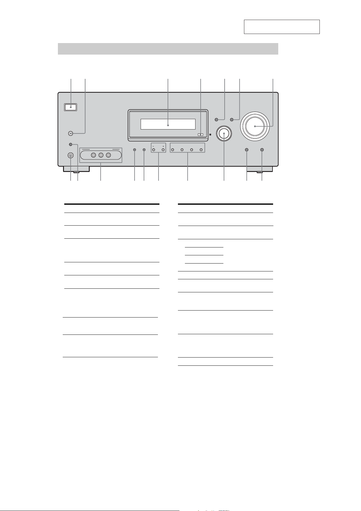
Front panel
SECTION 2
GENERAL
Thia section is extracted from
instruction manual.
SPEAKERS
(ON/OFF)
AUTO CAL MIC
PHONES
VIDEO 2 IN/PORTABLEAV IN
VIDEO L AUDIO R
MEMORY/
ENTER
TUNING
MODE
RHRIRK
Name Function
" /
(on/standby)
# SPEAKERS
(ON/OFF)
$ Display The current status of the
% Remote sensor Receives signals from
& DISPLAY Press to select information
' INPUT MODE Press to select the input
( MASTER
VOLUME
) MUTING Press to turn off the sound
Presstoturn thereceiveron
or off.
Press to turn the speaker
system on or off.
selectedcomponentora list
of selectable items appears
here.
remote commander.
displayed on the display.
mode when the same
components are connected
to both digital and analog
jacks.
Turn to adjust the volume
level of all speakers at the
same time.
temporarily.
PressMUTINGagainto
restore the sound.
TUNING 2CH A.F.D. MOVIE MUSIC
RTRERG
RB
Name Function
* AUTO CAL Press to activate the Auto
+ INPUT
SELECTOR
, 2CH Press to select a sound
A.F.D.
MOVIE
MUSIC
- TUNING +/– Press to scan a station.
. TUNING M ODE Press to select the tuning
/ MEMORY/
ENTER
0 VIDEO 2 IN/
PORTABLEAVIN
jacks
1 AUTO CAL MIC
jack
2 PHONES jack Connects to headphones.
DISPLAY INPUT MODE
INPUT SELECTOR
AUTO CAL
R
Calibration function.
Turn to select the input
source to play back.
field.
mode.
Press to store a station or
enter the selection when
selecting the settings.
Connect to a portable
audio/video component
such as a camcorder or
video game.
Connects to the supplied
optimizer microphone for
the Auto Calibration
function.
MASTERVOLUME
MUTING
4
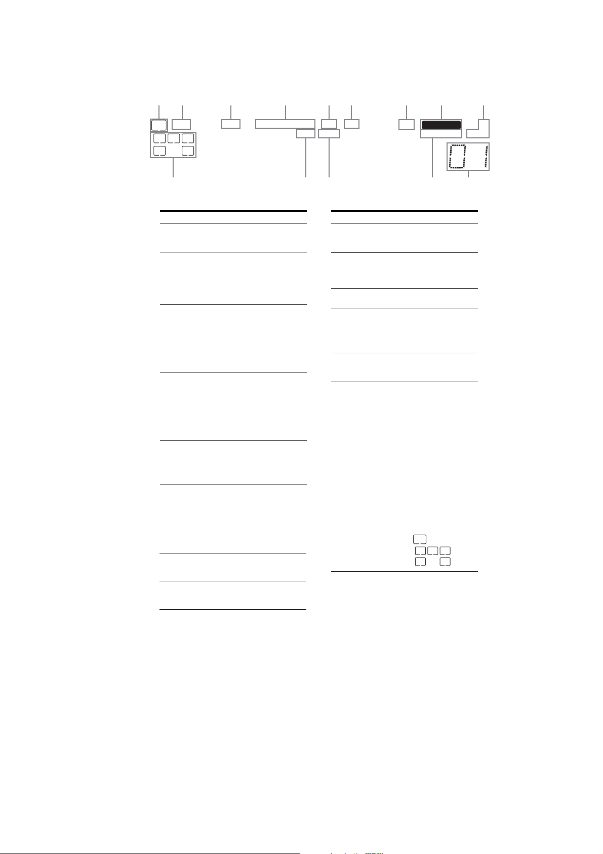
About the indicators on the display
STR-K7200
SW
LFE
LCR
S
SR
SL
Name Function
" SW Lights up when the audio signal
# LFE Lights up when the disc being
$ D Lights up when the receiver is
% PL/
PLII
& OPT Lights up when INPUT MODE
' DTS Lights up when the receiver is
( CAT Lights up when category mode
) MEMORY Lights up when a memory
is output from the SUB
WOOFER jack.
played back contains an LFE
(Low Frequency Effect)
channel and the LFE channel
signal is actually being
reproduced.
decoding Dolby Digital signals.
Note
When playing a Dolby Digital
formatdisc,besurethatyou
have made digital connections
and that INPUT MODE is set to
“AUTO”.
“PL”lightsupwhenthe
receiver applies Pro Logic
processing to 2 channel signals
in order to output the center and
surroundchannel signals.
“PLII” lights up when the
ProLogicIIMovieorMusic
decoder is activated.
isset to “AUTO” and the source
signal is a digital signal being
input through the OPTICAL
jack.
decoding DTS signals.
Note
When playing a DTS format
disc, be sure that you have made
digital connections and that
INPUT MODE is set to
“AUTO”.
is set to “ONE CAT” during
XM Radio operation.
function, such as Preset
Memory, etc., is activated.
D
PLII
HDMI
COAX
DTSOPT
CAT
PL
TRGR RE RRB
Name Function
* Tuner
indicators
+ Preset
station
indicators
, D.RANGE Lights up when dynamic range
- COAX Lightsup when INPUT MODE
. HDMI Lightsup when the receiver
/ Playback
channel
indicators
L
R
C
SL
SR
S
Lights up when using the
receiver to tune in radio stations,
etc.
Lights up when using the
receiver to tune in radio stations
you have preset. For details on
presetting radio stations, see.
compression is activated.
isset to “AUTO” andthe source
signal is a digital signal being
input through the COAXIAL
jack.
recognizes a component
connectedvia an HDMI INjack.
The letters (L, C, R, etc.)
indicate the channelsbeing
played back. The boxes around
the letters vary to show how the
receiver downmixes the source
sound.
Front Left
Front Right
Center (monaural)
Surround Left
Surround Right
Surround (monaural or the
surround components obtained
by Pro Logic processing)
Example:
Recording format (Front/
Surround): 3/2.1
Sound Field: A.F.D. AUTO
SW
SL SR
MEMORY
D.RANGE
LCR
ST
MONO
5
STR-K7200
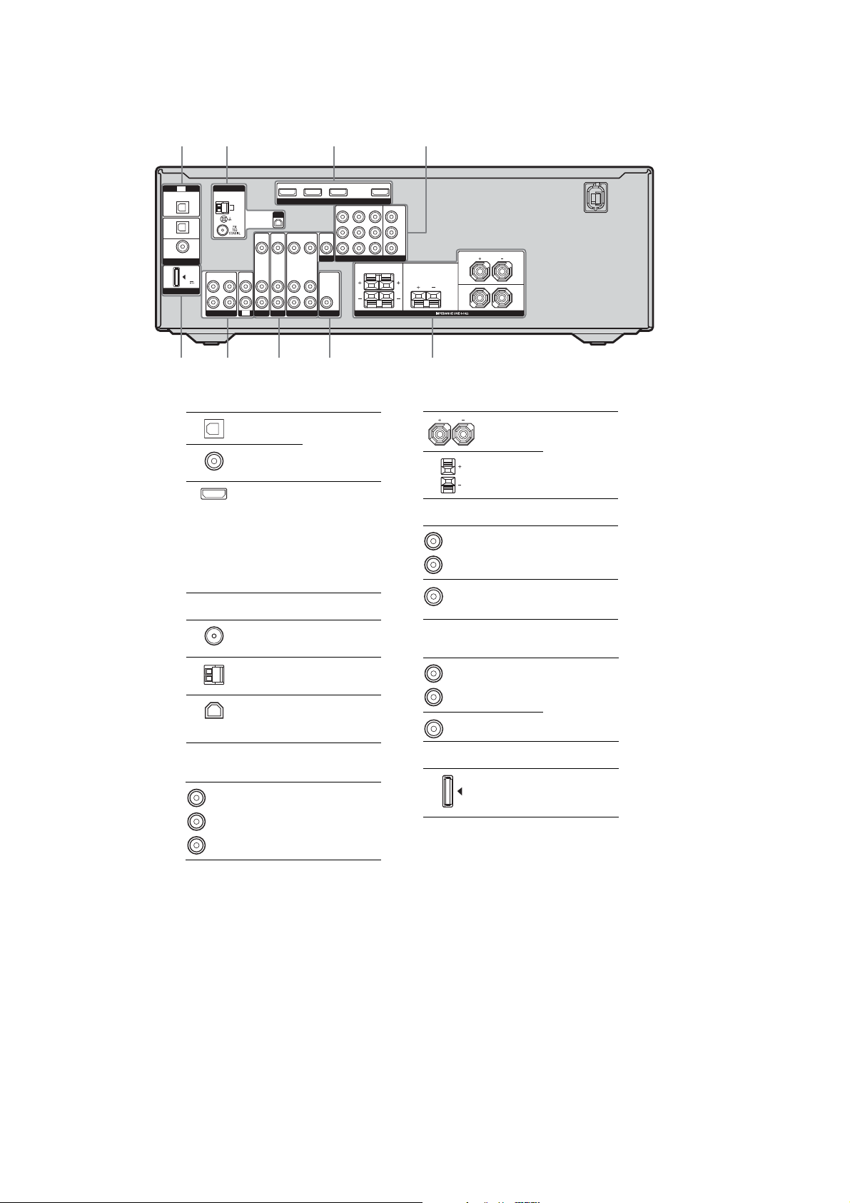
Rear panel
OPTICAL
IN
SAT
IN
OPTICAL
DVD
IN
COAXIAL
DIGITAL
DMPORT
TV
(ASSIGNABLE)
DC5V
0.7A MAX
ANTENNA
OUT IN IN
L
R
SA-CD/CD/CD-R
AM
SAT IN DVD IN BD IN OUT
XM
VIDEO
VIDEO
VIDEO
IN
IN
OUT
AUDIO
AUDIO
AUDIO
IN
IN
OUT
TV
SAT
DVD
VIDEO 1
VIDEO
AUDIO
" DIGITAL INPUT/OUTPUT section
OPTICAL
IN jacks
COAXIAL IN
jack
HDMI IN/
OUT* jacks
# ANTENNA section
FM
ANTENNA
jack
AM
ANTENNA
terminals
XM terminal Connects to the XM
Connects to a DVD
player, etc. The
COAXIAL jack
provides a better
sound quality.
Connects to a DVD
player, Blu-ray disc
player, etc. The
image is output to a
TV or a projector
while the sound can
be outputfrom a TV
or/and speakers
connected to this
receiver.
Connects to the
supplied FM wire
antenna.
Connects to the
supplied AM loop
antenna.
Mini-Tuner and
Home Dock (not
supplied).
HDMI
SAT IN DVD IN VIDEO 1 IN MONITOR OUT
VIDEO
IN
OUT
MONITOR
AUDIO
IN
OUT
SUB WOOFER
COMPONENT VIDEO
SURROUND CENTER
LR
Y
P
B
/
B
C
PR/
C
R
SPEAKERS
FRONT
L
R
% SPEAKERS section
& AUDIO INPUT/OUTPUT section
AUDIO IN/
White (L)
OUT jack
Red (R)
AUDIO OUT
Black
jack
' VIDEO/AUDIO INPUT/OUTPUT
section
AUDIO IN/
White (L)
OUT jacks
Red (R)
VIDEO IN/
Yellow
OUT* jacks
Connects to the
supplied speakers.
Connects to a
Super Audio CD
player, etc.
Connects to the
supplied sub
woofer.
Connects to a
VCR, DVD player,
etc.
$ COMPONENT VIDEO INPUT/
OUTPUT section
Green
(Y)
Blue
(P
B/CB)
Red
(P
R/CR)
Y,PB/CB,PR/CR
IN/OUT* jacks
Connects to a DVD
player, TV,
satellite tuner, etc.
You can enjoy high
quality image.
( DMPORT
Connects to a
DIGITAL MEDIA
PORT adapter.
* You can watch the selected input image when you
connect the HDMI OUT or MONITOR OUT jack
to a TV.
6
STR-K7200
Remote commander
You can use the supplied RM-AAU021
Remote Commander to operate the receiver
and to control the Sony audio/video
components that the remote is assigned to
operate.
R
RB
RT
XB
X
RM
RL
RK
RI
RH
RG
RE
TV INPUT
SLEEP
VIDEO 1 VIDEO 2 BD DVD
SAT TV SA-CD/CD TUNER
2CH A.F.D.
123
46
78
>10
CLEAR
DISPLAY
0
RETURN/EXIT
TV CH –
PRESET –
TUNING –
TV
TV
DMPORT
AV
SYSTEM STANDBY
MOVIE MUSIC
5
9
MEMORY
0/10
ENTER
TOOLS/
OPTIONS
MENU/HOME
– CATEGORY +
REPLAY ADVANCE
CATEGORY MODE
).N
9Y
THEATER
DVD/BD
AUTO CAL
D.TUNING
D.SKIP
AMP MENU
TV VOL
MASTER VOL
PRESET +
TUNING +
FM MODE
MENU
MUTING
TV CH +
Name Function
" TV /
(on/standby)
AV /
(on/standby)
# /
(on/standby)
$ Input buttons Press one of the buttons to
Press TV / and TV (.)at
the same time to turn the TV
on or off.
Presstoturnonoroffthe
Sonyaudio/video components
that the remote is assigned to
operate.
If you press / (#)atthe
same time, it will turn off the
receiver and other Sony
components (SYSTEM
STANDBY).
Note
The function of the AV /
switch changes automatically
each time you press the input
buttons ($).
Press to turn the receiver on or
off.
To turn off all Sony
components, press / and
AV / (")atthesametime
(SYSTEM STANDBY).
select the component you
want to use. When you press
any of the input buttons, the
receiver turns on. The buttons
are factory assigned to control
Sony components as follows.
You can change the button
assignments following the
steps in “Changing button
assignments”.
Button Assigned Sony
DMPORT DIGITALMEDIA
VIDEO 1 VCR (VTR mode 3)
VIDEO 2 VCR (VTR mode 2)
BD Blu-ray disc player
DVD DVD player
SAT Digital Satellite
TV TV
SA-CD/CD Super Audio CD/
TUNER Built-in tuner
component
PORTadapter
Receiver
CD player
Name Function
% 2CH Press to select a sound field.
A.F.D.
MOVIE
MUSIC
& THEATER Press to enjoyoptimal image
' DVD/BD
MENU
AUTO CAL Pressto activate the Auto
( D.TUNING Press to enter direct tuning
D.SKIP Pressto skip a disc when
) AMP MENU Press to display the menu of
* ENTER Press to enter the value after
MEMORY Presstostoreastation.
+ MUTING Press to turn off the sound
, TV VOL
a)
+
/–
MASTER
a)
VOL +
suited for movies and to
output the sound from the
speakers connected to this
receiver automatically.
Note
This button will only function
if your TV is compatible with
Theater Mode.
Refer to the operating
instructions supplied with the
TV for details.
Press to display the menu of
the DVD or Blu-ray disc on
the TVscreen. Then, use 7, W,
#, C and (1) to perform
menu operations.
Calibration function.
mode.
using a multi-disc changer.
the receiver. Then, use 7, W,
#, C and (1) to perform
menu operations.
selecting a channel, disc or
track using the numeric
buttons of the TV, VCR or
satellite tuner.
temporarily.
Press MUTING again to
restore the sound.
Press MUTING and TV (.)
at the same time to activate
the TV’s muting function.
Press TV VOL +/– and TV
(.) at thesame time toadjust
the volume level of the TV.
Press to adjust the volume
/–
level of all speakers at the
same time.
7
STR-K7200
Name Function
- /
REPLAY /
ADVANCE
N/.
)
9
Y
TV CH +/– PressTVCH+/–andTV(.)
CATEGORY
+/–
PRESET +/– Press to select
TUNING +/– Press to scan a station.
CATEGORY
MODE
FM MODE Press to select the FM
. TV Press TV and the button with
b)
PresstoskipatrackoftheCD
player, DVD player orBlu-ray
disc player.
Press to replay the previous
scene or fast forward the
current scene of the VCR,
DVD player or Blu-ray disc
player.
b)
Press to
– search tracks in the forward/
reverse directionof the DVD
player.
– start fast forward/rewind of
the VCR, CD player or Bluray disc player.
a)b)
Press to start playback of the
VCR,CD player, DVD player,
or Blu-ray disc player.
b)
Press to pause playback or
recording of the VCR, CD
player, DVD player orBlu-ray
disc play er. (Also starts
recording with components in
recording standby.)
b)
Presstostopplaybackofthe
VCR, CD player, DVD player
or Blu-ray disc player.
at the same time to select
preset TV channels.
Press to select a category for
XM Radio.
– preset stations.
– preset channels of the VCR
or satellite tuner.
Press to select the category
mode for XM Radio.
monaural or stereo reception.
orange printing at the same
time to enable TV operation.
Name Function
/ MENU/HOME Press to display the menu of
0 RETURN/
EXIT 0
),
1
7/W/#/C
2 DISPLAY Press to select information
the VCR, DVD player,
satellite tuner or Blu-ray disc
player on the TV screen.
Press MENU/HOME and TV
(.) at the same time to
display the TV’s menu.
Then, use 7, W, #, C and
(1) to perform menu
operations.
Press to
– return to the previous menu.
– exit the menu while the
menu or on-screen guide of
the VCR, D V D player,
satellite tuner or Blu-ray
disc player is displayed on
the TV screen.
PressRETURN/EXITand TV
(.) atthe same time to return
to the previous menu or exit
the TV’s menu while the
menu is displayed on the TV
screen.
After pressing DVD/BD
MENU ('), AMP MENU
()), or MENU/HOME (/
press 7, W, # or C to selectthe
settings. Then, press to
enter the selection if you have
pressed DVD/BD MENU or
MENU/HOME previously.
Press also to enter the
selection of the receiver,
VCR, satellite tuner, CD
player, DVD player or Bluraydiscplayer.
displayed on the TV screen of
the VCR, satellite tuner, CD
player, DVD player or Bluraydiscplayer.
PressDISPLAY and TV (.)
at the same time to display
TV’s information on the TV
screen.
Name Function
3 TOOLS/
OPTIONS
[
4
>10 Press to select track numbers
CLEAR Press to clear a mistake when
5 Numeric
buttons
(number 5
6 TV INPUT PressTVINPUTandTV(.)
SLEEP Pressto activatethe Sleep
a)
The number 5, MASTE R VOL +, TV VOL +, and
) buttonshave tactile dots. Use the tactile dots
as references when operating the receiver.
b)
This button is also available for DIGITALMEDIA
PORT adapter operation. For details on the
functionof the button, refer to the operating
instructions supplied with the DIGITAL MEDIA
PORT adapter.
Press to display and select the
options of the DVD player or
Blu-ray disc player.
Press TOOLS/OPTIONS and
TV (.) at the same time to
display the options applicable
to the Sony TV.
Press to input the decimal
point for channel numbers of
the Digital CATV terminal.
Press
[ and TV (.)atthe
sametimeto inputthedecimal
point for the channel numbers
of the TV.
over 10 of the CD player.
you press the incorrect
numeric button.
Press to
– preset/tune to preset
a)
)
stations.
– select track numbers of the
CD player, DVD player or
Blu-ray disc player. Press
0/10 to select track number
10.
– select channel numbers of
the VCR or satellitetuner.
Press the numeric buttons and
TV (.) at the same time to
select the TV channels.
at the same time to select the
inputsignal(TVinputor
video input).
Timer function and the
duration which the receiver
turns off automatically.
Notes
•Some functions explained in this section may not
work depending on the model.
•The above explanation is intendedto serve as an
example only. Therefore, depending on the
component, the above operationmay not be
possibleor may operate differentlythan described.
8
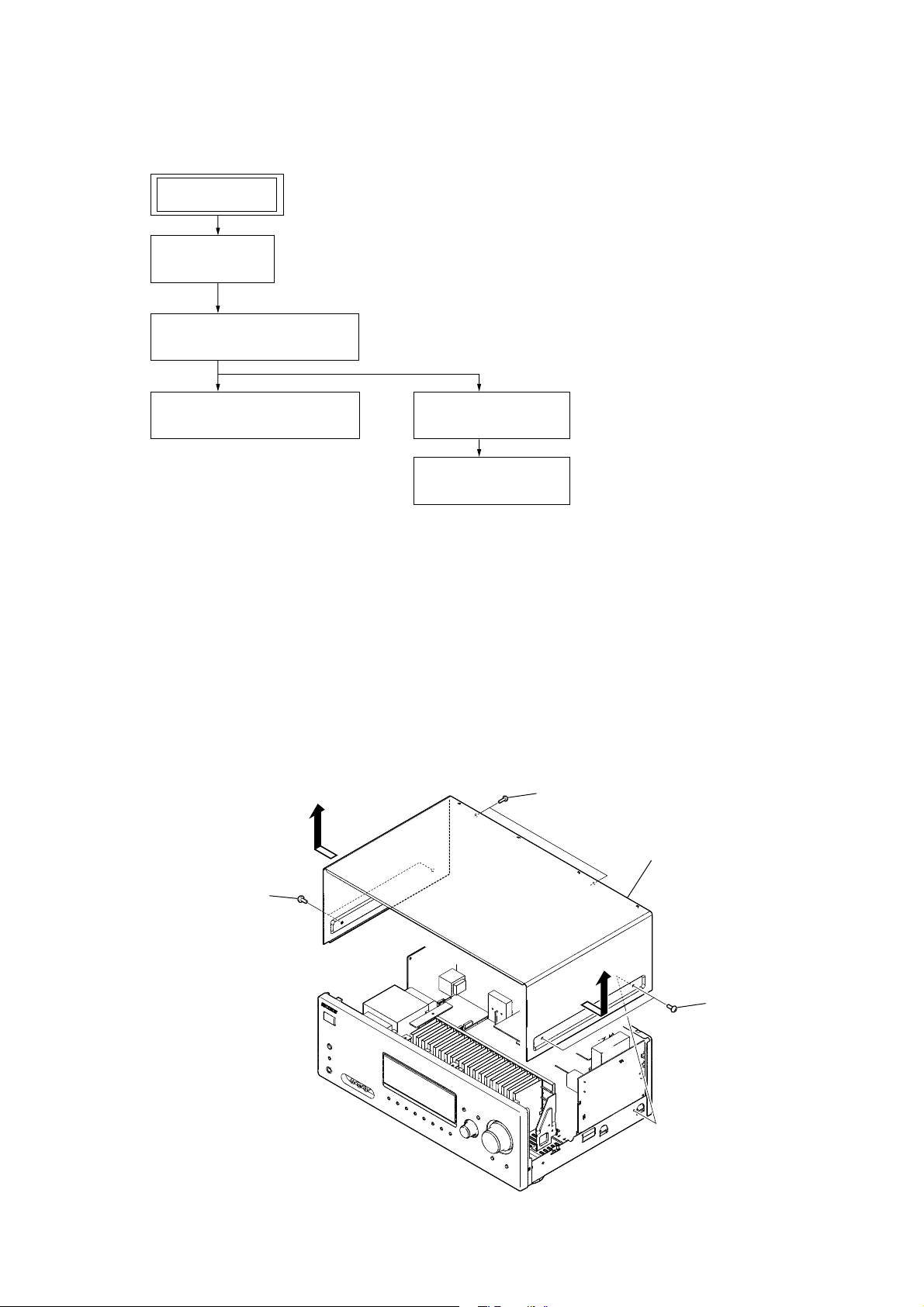
DISASSEMBLY
• This set can be disassembled in the order shown below.
3-1. DISASSEMBLY FLOW
SET
3-2. CASE
(Page 9)
3-3. BACK PANEL BLOCK
(Page 10)
STR-K7200
SECTION 3
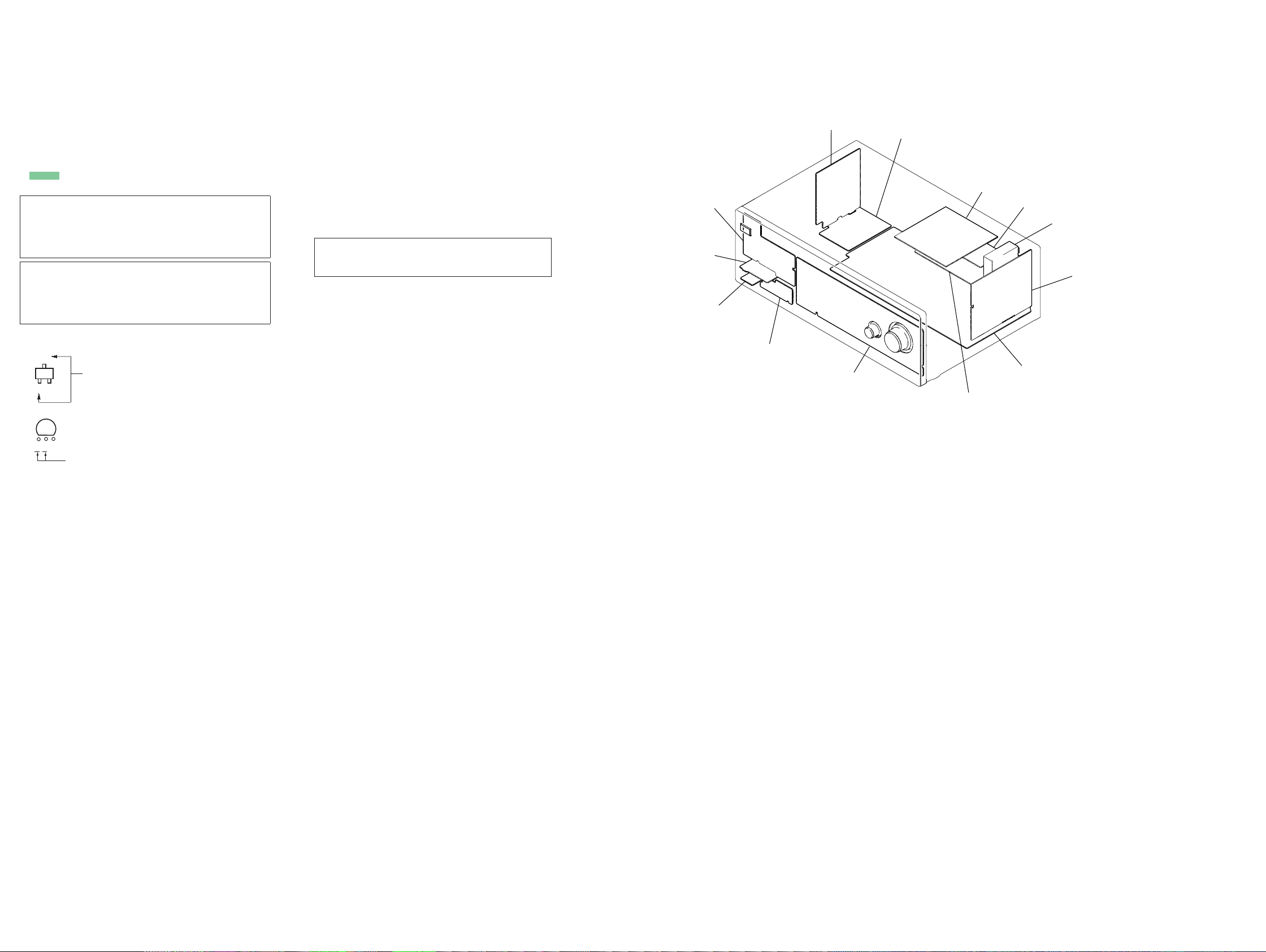
3-4. FRONT PANEL BLOCK
(Page 10)
Note: Follow the disassembly procedure in the numerical order given.
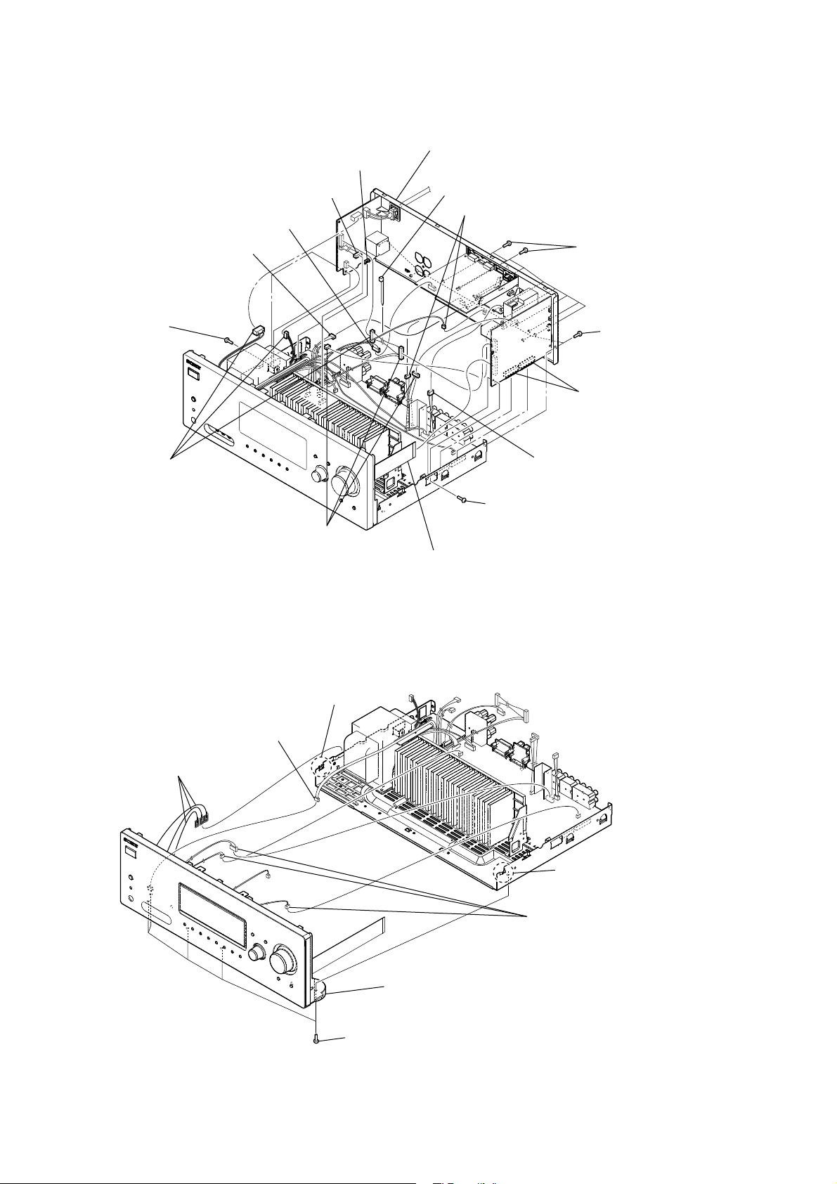
3-5. MAIN BLOCK
(Page 11)
3-6. MAIN BOARD
(Page 11)
3-2. CASE
two screws
(BVTP3 × 8)
case
two screws
(BVST4 × 8)
two screws
(BVST4 × 8)
9
STR-K7200
3-3. BACK PANEL BLOCK
connector
(CNP103)
screw
R
(BVTP3 × 8)
(CNP912)
connector
(CN3509)
connector
connector
RG
(CNP911)
back panel block
RH
clamp
two connectors
(CNP203, CNP204)
nine screws
RT
(BVTP3 × 8)
five screws
RT
(BVTP3 × 8)
two connectors
RE
(CNS501, CNS502)
three connectors
(CNP902, CNP910, CNP913)
(CNP504, CNP505, CNP512)
3-4. FRONT PANEL BLOCK
three leads (with connector)
(TP202, TP790, TP2000)
three connectors
connector
(CN790)
claw
screw
RB
(BVTP3 × 8)
wire (flat type) (17 core)
(CNS510)
connector
(CN102)
10
front panel section
five screws
(BVTP3 × 8)
claw
three connectors
(CNP430, CNP500, CNP930)
3-5. MAIN BLOCK
(CN790)
connector
three screws
(BV3)
two connectors
(CNP921, CNP940)
two screws
(BV3)
main block
STR-K7200
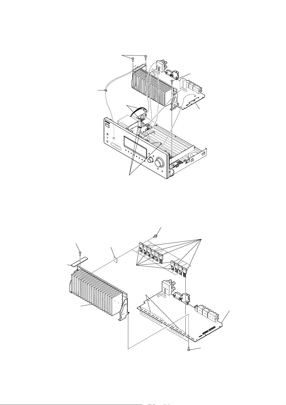
3-6. MAIN BOARD
screw
(BV3)
wire route board
heatsink assy
three connectors
(CNP430, CNP500, CNP930)
ten sheets
five transistor MP1620-OPY-MK
(Q654, Q704, Q754, Q804, Q854)
Remove the
thirty solders.
ten screws
(transistor)
five transistor MN2488-OPY-MK
(Q653, Q703, Q753, Q803, Q853)
MAIN board
R
two screws
(BVTP3 × 8)
11
STR-K7200
SECTION 4
TEST MODE
TUNER AM STEP CHANGE (9 kHz/10 kHz) MODE
The AM tuning interval can be changed over 9 kHz or 10 kHz.
Procedure:
1. Press the [
] button to turn on the main power.
?/1
2. Turn the [INPUT SELECTOR] dial to select the “AM”.
3. Press the [
4. While pressing the [TUNING MODE] button, press the [
] button to turn off the main power.
?/1
?/1
button to turn on the main power.
5. The AM turning interval changed over 9 kHz or 10 kHz.
FL CHECK MODE
All fl uorescent segments are tested. When this test is activated, all
segments turn on at the same time, then each segment turns on one
after another.
Procedure:
1. When pressing the [TUNING MODE] and [DISPLAY] buttons, press the [
] button to turn on the main power.
?/1
2. All segments turn on.
LFE
SW
L CR
S
SR
SL
SB SBRSBL
SP A
SP B
D EX
PL II xPL
OPT
HDMI COAX
DTS-ES 96 / 24
CAT
NEO:6 SAT D.RANGE
MEMORY
dB
k Hz
mft.
MHz
RDS ST
MONO
3. Turn the [INPUT SELECTOR] dial.
4. Test pattern 1 turn on.
k
m
MHz
RDS ST
MONO
LFE
L R
S
D EX
SP B
PL II x
HDMI COAX
DTS-ES
NEO:6 SAT D.RANGE
5. Turn the [INPUT SELECTOR] dial once again.
6. Test pattern 2 turn on.
SW
C
SL SR
SB SBRSBL
D
DTS
PL
CAT
MEMORY
dB
Hz
ft.
ST
KEY CHECK MODE
This mode is used to check the key.
Procedure:
1. While pressing the [SPEAKERS (ON/OFF)] and [2CH] buttons, press the [
] button to turn on the main power.
?/1
2. The message “REST 13” appears.
]
3. Every pressing of any button other than the [
?/1
down the buttons. The buttons which are already counted once
are not counted again.
4. When all buttons are pressed, the message “REST 00” appears.
SWAP ALL MODE
When this mode is used, output the audio signal of front L/R channel to all channel.
Procedure:
1. While pressing the [MEMORY/ENTER)] and [DISPLAY]
buttons, press the [
] button to turn on the main power.
?/1
2. The message “DSP TEST” appears.
3. Press the [AMP MENU] button on the remote commander, and
the message “9_DSPTST” appears.
4. Press the [b] button on the remote commander to enter the
DSP test mode menu.
5. Press the [v] button on the remote commander twice to enter
the swap mode, and the message “SWP.AUTO” appears.
6. Press the [b] button on the remote commander twice to select
“SWP.[]ALL”.
SHIPMENT MODE
All preset contents are cleared when this mode is activated. Use
this mode before returning the product to clients upon completion
of repair.
Procedure:
1. While pressing the [SPEAKERS (ON/OFF)] and [MUSIC] buttons, press the [
] button to turn on the main power.
?/1
2. The message “CLEARING” appears.
] button counts
7. Turn the [INPUT SELECTOR] dial once again. All segments
turn off.
8. Every turning of the [INPUT SELECTOR] dial turns on each
segment one after another on the same order.
S.F. CLEAR MODE
The preset sound fi led is cleared when this mode is activated. Use
this mode before returning the product to clients upon completion
of repair.
Procedure:
1. While pressing the [2CH] button, press the [
] button to turn
?/1
on the main power.
2. The message “S.F CLR.” appears and initialization is performed.
VERSION CHECK MODE
When this mode is used the model, the destination and the software
version number are displayed.
Procedure:
1. While pressing the [SPEAKERS (ON/OFF)] and [DISPLAY] buttons, press the [
] button to turn on the main power.
?/1
2. The model, the distination and the software version number
appear.
DCAC FACTORY TEST MODE
DCAC Factory Test mode have two stages:
1. DCAC DSP Data Line Checking
2. DCAC board Checking
Start Pass Pass
DSP Data Line
Check
Auto Cal Mic
Check
END
Factory Test System Setup
Receiver
DCAC MIC
SPK Front Left
1. When power off :
While pressing the [MEMORY/ENTER] and [MOVIE] but-
tons, press the [
] button to turn on the main power .
?/1
“DCAC FTM” appears.
Afterward, press the [TUNING MODE] to start DCAC factory
test mode.
12

1. DCAC DSP Data Line Checking
After press the [TUNING MODE] button, DCAC Factory test
mode will start, below display will show:
“DCAC x” x = 1, 2, 3, 4
If there is error happen, below display will show:
“ERR SD0x” x = 1 → D1501 or R1530 problem
x = 2 → D1502 problem
x = 3 → D1503 problem
x = 4 → D1504 problem
2. DCAC board Checking
Connect front left speaker of the receiver and AUTO CAL microphone. Turn [MASTER VOLUME] jog, there will be test tone
sound output from front left speaker, and the display will change
accordingly.
“AD - xxx” xxx = 0 to 255 (depends on loudness of test tone)
RE-BOX CLASSIFICATION TEST MODE
Procedure:
1. While pressing the [MEMORY/ENTER] and [INPUTMODE]
buttons, press the [
2. The message “R.BOX[][][]XX” appears.
XX: times set powered on
] button to turn on the main power.
?/1
STR-K7200
VACS CONTROL TEST MODE
The VACS feature of the amplifi er is turned off purposely.
Procedure:
1. While pressing the [MEMORY/ENTER] and [2CH] buttons,
press the [
2. The message “VACS OFF” appears.
] button to turn on the main power.
?/1
13

STR-K7200
SECTION 5
ELECTRICAL CHECK
FM AUTO STOP CHECK
signal
generator
Procedure:
1. Turn on the set.
2. Input the following signal from signal generator to FM antenna
input directly.
Carrier frequency: A = 87.5 MHz, B = 98 MHz, C = 108 MHz
Deviation : 75 kHz
Modulation : 1 kHz
ANT input : 1 kHz
Note: Use 75 ohm coaxial cable to connect signal generator and the set.
You cannot use video cable for checking.
Use signal generator whose output impedance is 75 ohm.
3. Set to FM tuner function and scan the input FM signal with
automatic scanning.
4. Confi rm that input frequency of A, B and C are detected and
automatic scanning stops.
set
When the station signal is received in good condition, automatic
scanning stops.
14
STR-K7200
STR-K7200
1515
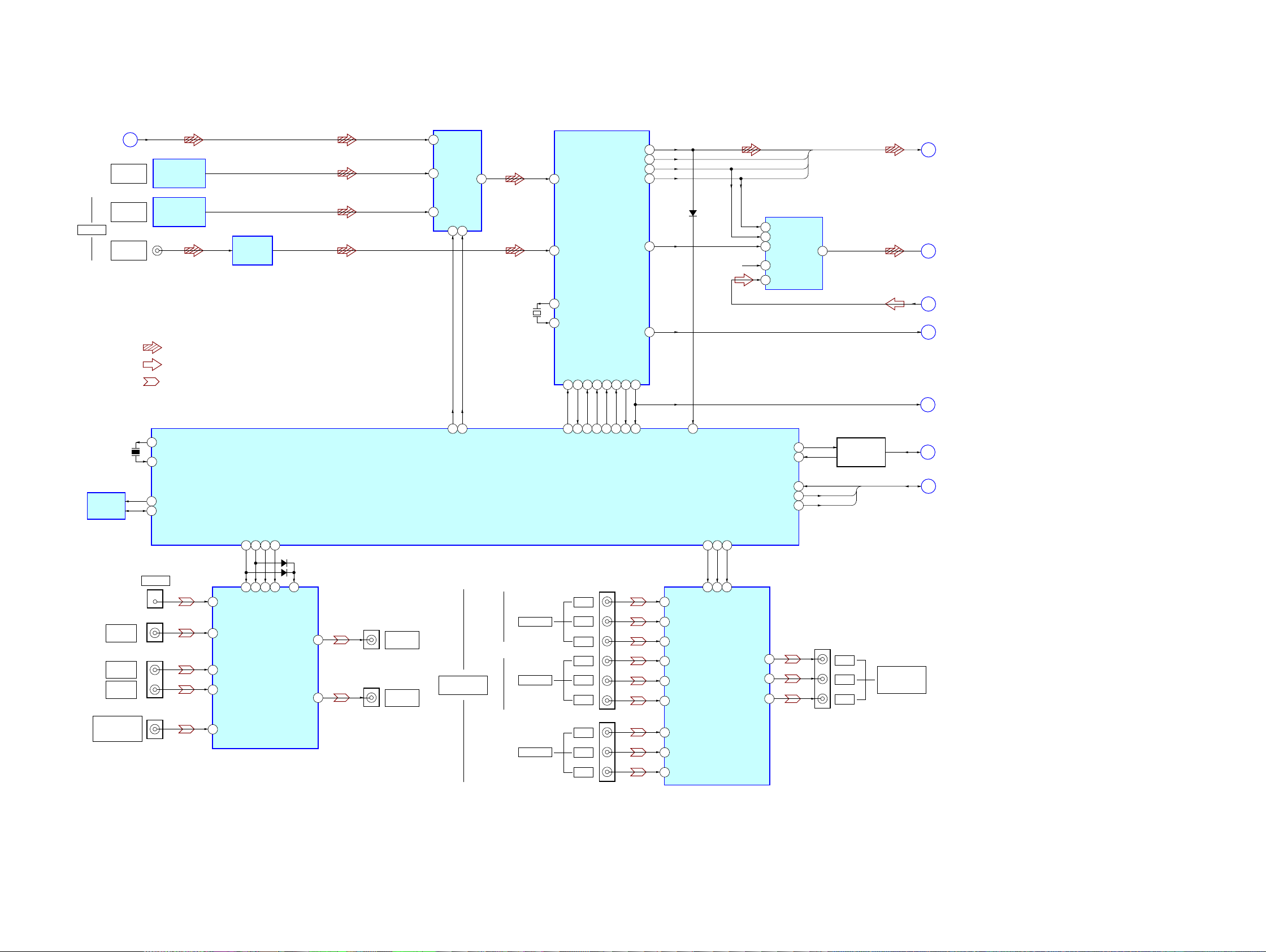
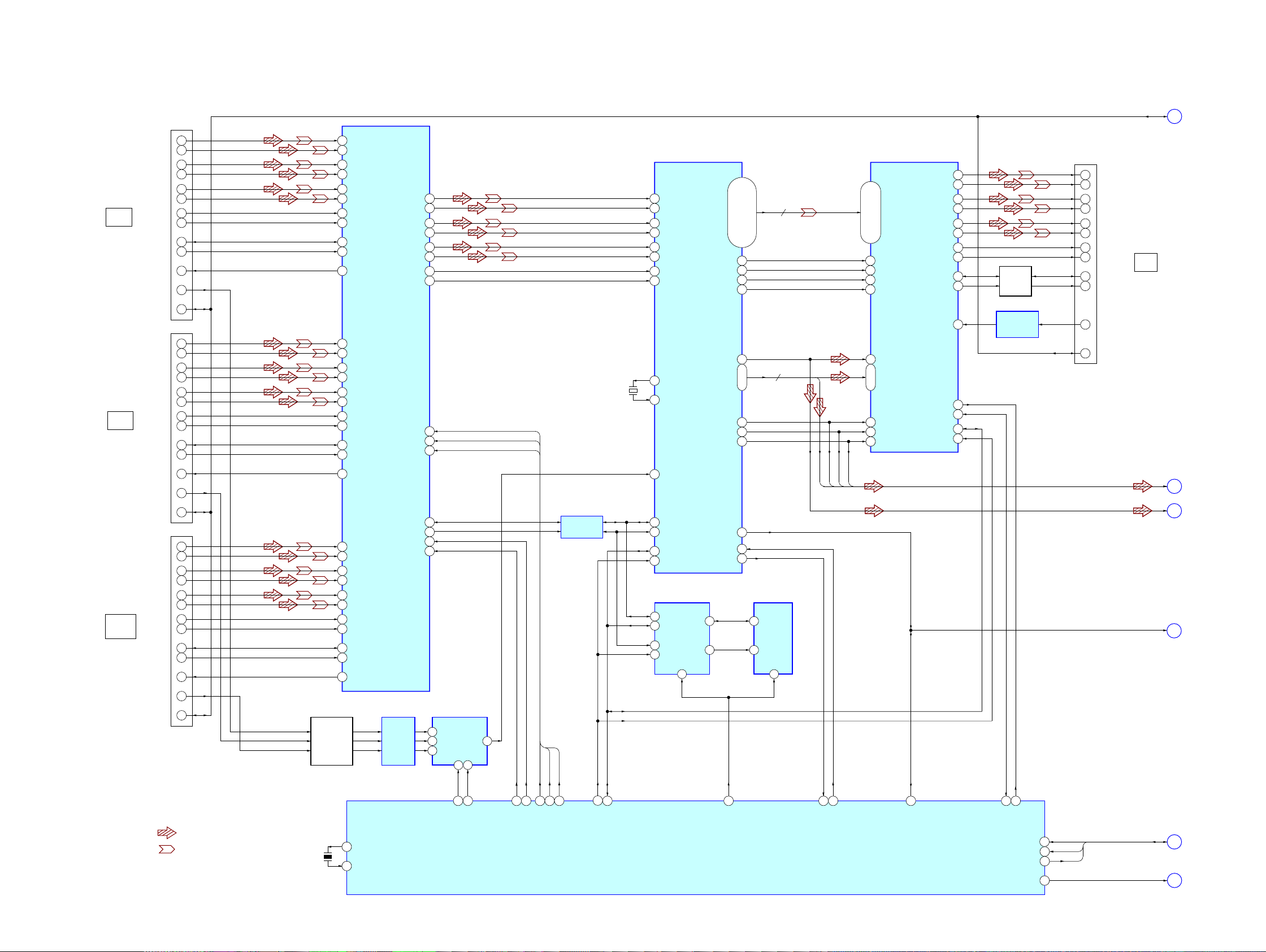
6-1. BLOCK DIAGRAM - MAIN Section -
SECTION 6
DIAGRAMS
EEPROM
IC1131
SYSTEM CONTROLLER
IC1010 (1/4)
DIGITAL OPTICAL
RECEIVER
IC1352
DIR_DO
DIR_DI
DIR_CLK
DIR_CE(LAT)
DIR ERROR
DIR_XMODE (RESET)
DIR_XSTATE
DIR DATA0
63
DATA0, BCK
LRCK, CKOUT
DOUT
7
SCKI
12
BCK
8
LRCK
13
VINL
14
VINR
6
XMCK
20
DATAO
16
BCK
14
LRCK
15
CKOUT
13
AUDIO
24
46
TV OPT
IN
DIGITAL OPTICAL
RECEIVER
IC1351
OPT SAT
IN
SCHMITT
TRIGGER
IC1303
DIGITAL AUDIO
INTERFACE RECEIVER
IC1301
DIN2
J1301
5
COAX IN
DVD
DIGITAL
A/D CONVERTER
IC1401
21
22
X1301
12.288MHz
XOUT
XIN
DIRCKST
39
D1301
57
58
X1
X0
98
EEPROM DATA
78
EEPROM CLK
X1101
12.5MHz
A
• SIGNAL PATH
: AUDIO (ANALOG)
: AUDIO (DIGITAL)
• R-ch is omitted due to same as L-ch.
DATA SELECTOR
IC1302
1C2
5
1C3
3
1C1
6
DIN0
3
1Y
7
2
B
CKSEL0
DOUTDICLKCEXMODE
XSTATE
ERROR
14
A
TC74HC153_A
36
TC74HC135_B
35
CEC DATA
SWITCH
Q1103 – 1106
HDMI_TX
HDMI_RX
HDMI RESET
104
103
103
29
CEC OUT
CEC IN
88
AUDIO
A_AUDIO
D_AUDIO
B
N
M
ERR
C
CEC
D
48 47 45 46 492938
RESET, TX, RX
E
J
SPDIF
R-CH
35 36 38 37 48 17 34
VIDEO 1 IN
VIDEO 1
VIDEO IN
VIDEO 2 IN/
PORTABLE A V IN
VIDEO
DVD
VIDEO IN
SAT
VIDEO IN
DMPORT_VIDEO
17
J1302 (1/2)
J210 (1/2)
J211 (1/2)
J298 (1/2)
DMPORT
VIDEO 1
VIDEO OUT
MONITOR
VIDEO OUT
J210 (2/2)
J220 (1/2)
J221
J211 (2/2)
VIDEO AMP
IC210
VIN3
7
VIN1
13
VIN5
3
VIN4
5
VIN2
9
VOUT1
1
VOUT2
15
SW114SW210SW34SW46SW5
2
34
V_SW133V_SW232V_SW331V_SW4
D211
D210
: VIDEO
COMPONENT
VIDEO
VIDEO AMP
IC220
CH1 IN1
1
CH2 IN1
8
CH3 IN1
17
CH1 IN2
3
CH2 IN2
14
CH3 IN2
15
CH1 IN3
5
CH2 IN3
12
CH3 IN3
13
SW12SW2
4PS23
35
COMP_S136COMP_S237PS(V-MUTE)
PB/CB
Y
P
R/CR
DVD IN
P
B/CB
Y
P
R/CR
SAT IN
P
B/CB
Y
P
R/CR
J220 (2/2)
CH1 OUT
24
CH2 OUT
22
CH3 OUT
20
P
B/CB
Y
P
R/CR
COMPONENT
VIDEO
MONITOR OUT
(Page 16)
(Page 17)
(Page 17)
(Page 18)
(Page 17)
(Page 17)
(Page 16)
(Page 16)
STR-K7200
STR-K7200
1616
6-2. BLOCK DIAGRAM - HDMI Section -
• SIGNAL PATH
: AUDIO (DIGITAL)
: VIDEO
HDMI CONTROLLER
IC3519
CN3501
HDMI
SAT IN
A32
52
B32
51
7
9
A33
55
B33
54
4
6
A34
58
B34
57
1
3
A31
49
B31
48
10
DATA0+
DATA0–
DATA1+
DATA1–
DATA2+
DATA2–
CLOCK+
CLOCK–
SDA (5V)
SCL (5V)
+5V POWER
HOT PLUG DET
18
CEC
13
12
16
15
HDMI
INPUT
SELECTOR
IC3503
55
P5V_SELA
56
P5V_SELB
SDA3
45
19
HPD3
44
SCL3
46
CN3502
HDMI
DVD IN
A22
71
B22
70
7
9
A23
74
B23
73
4
6
A24
77
B24
76
1
3
A21
68
B21
67
10
DATA0+
DATA0–
DATA1+
DATA1–
DATA2+
DATA2–
CLOCK+
CLOCK–
SDA (5V)
SCL (5V)
+5V POWER
HOT PLUG DET
18
CEC
13
12
16
15
SDA2
63
19
HPD2
62
SCL2
64
CN3503
HDMI
VIDEO 2/
BD IN
A12
9
B12
8
7
9
A13
12
B13
11
4
6
A14
15
B14
14
1
3
A11
6
B11
5
10
DATA0+
DATA0–
DATA1+
DATA1–
DATA2+
DATA2–
CLOCK+
CLOCK–
SDA (5V)
SCL (5V)
+5V POWER
HOT PLUG DET
18
CEC
13
12
16
15
SDA1
2
19
HPD1
80
SCL1
3
RX_HPD1
HDMI RECEIVER
IC3511
HDMI
TRANSCEIVER
IC3513
Y1
34
Z1
35
51
50
Y2
31
Z2
32
55
54
Y3
28
Z3
29
59
58
Y4
25
Z4
26
63
RXC+
RXC–
RX0+
RX0–
RX1+
RX1–
RX2+
RX2–
DSDA
DSCL
62
41
PWR5V
44
42
CSDA
CSCL
39
40
SCL_SINK
38
HPD_SINK
40
xOE
42
SDA_SINK
39
S1
21
S2
22
S3
23
LEVEL
SHIFT
IC3501
(1/2)
LEVEL SHIFT
IC3507
S [1]
S [2]
S [3]
SIGNAL SELECTOR
IC3504
2Y2
2
2Y3
4
2Y1
5
3
2-COM
10
9
A
B
21
51 52 53
S [1]
S [2]
S [3]
TMDS_S1
TMDS_S2
TMDS_S3
DATA SELECTOR
IC3521
EEPROM
IC3509
2Y1
5
2Y0
1
1Y1
14
1Y0
12
3
2-COM
13
1-COM
5
SDA
6
SCL
EEPROM1
10
A
7
WP
35
TMDS_OEB
54
RX_RST
19
MUTE
65
RX_INT
20
TX_INT
43
TX_RST
42
CSCL
27
CSDA
28
124 – 121,117 – 114,
111 – 108, 105 – 99,
96 – 92
QE0 – QE23
79 – 75, 70 – 67
65 – 61, 58 – 49
D0 – D23
ODCK
119
HSYNC
128
VSYNC
1
DE
127
SPDIF
70
SD0 – SD3
4
24
MCK
79
SCK
76
WS
75
MUTE
67
RESET
89
INT
91
IDCK
66
HSYNC
1
VSYNC
2
DE
80
74 – 71
SPDIF
5
SD0 – SD3
MCK
6
SCK
12
WS
11
10 – 7
TX0+
30
TX0–
29
7
9
TX1+
33
TX1–
32
4
6
TX2+
36
TX2–
35
1
3
TXC+
27
TXC–
26
10
HPD
DATA0+
DATA0–
DATA1+
DATA1–
DATA2+
DATA2–
CLOCK+
CLOCK–
SDA (5V)
SCL (5V)
HOT PLUG DET
CEC
18 19
12
16
15
13
DSDA
19
DSCL
20
INT
17
RESET
42
CSDA
44
CSCL
43
LEVEL
SHIFT
IC3501 (2/2)
LEVEL
SHIFT
Q3504
CN3504
HDMI
OUT
SPDIF
LRCK
MCK
BCK
SD0 – SD3
85
84
XTALIN
XTALOUT
X3501
28.322MHz
10RESET
RESET, TX, RX
D
13
11
XIN
XOUT
X3502
10MHz
B+ SWITCH
Q3505-3507
F
G
E
33TX
34RX
CEC
MUTE
SD0-3, MCK,
BCK, LRCK
J
41TX_5VPWR
K
5VPWR
(Page 15)
(Page 17)
(Page 15)
(Page 17)
(Page 15)
(Page 19)
STR-K7200
STR-K7200
1717
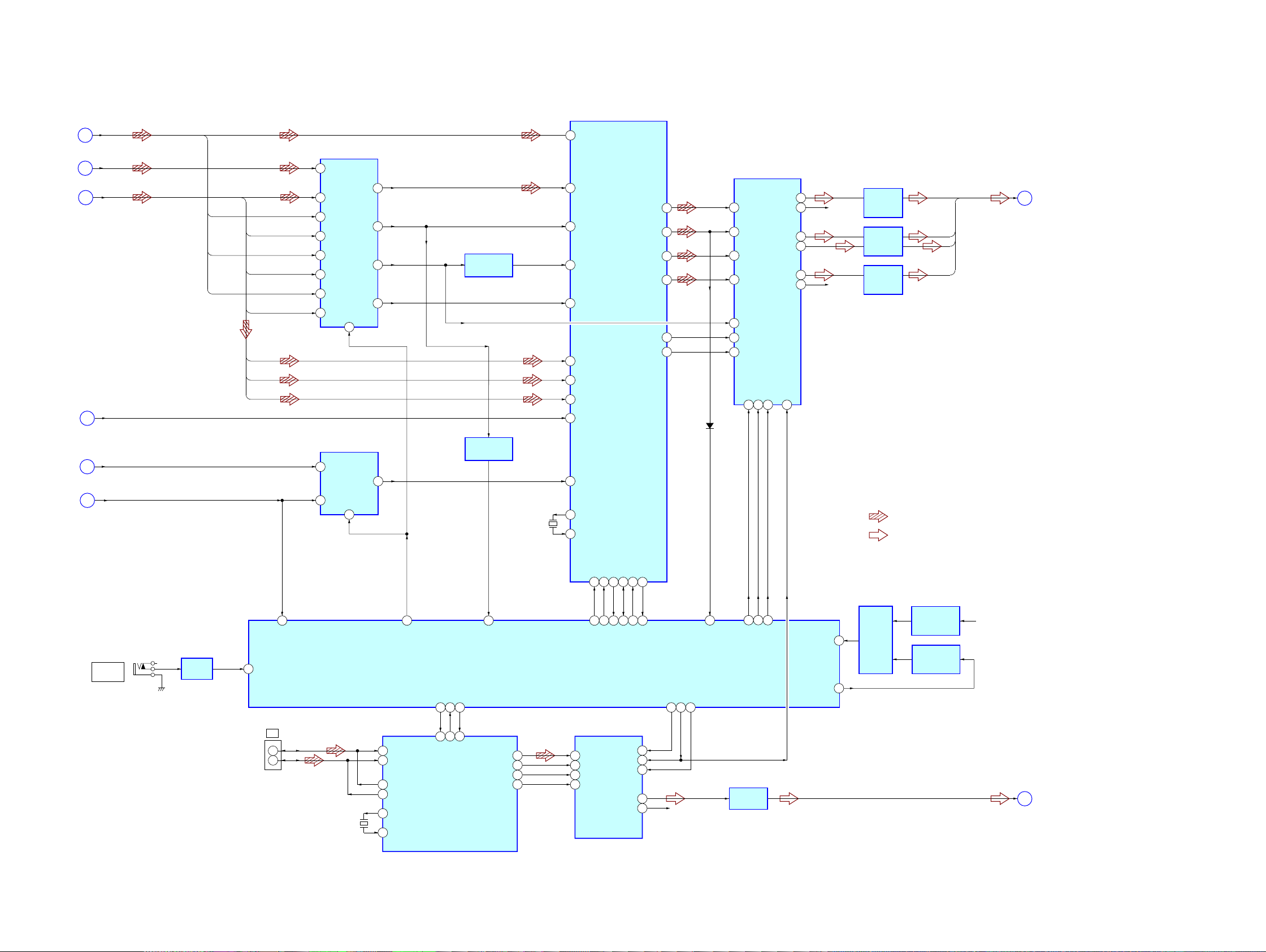
6-3. BLOCK DIAGRAM - DSP/XM Section -
A
M
DATA0, BCK, LRCK, CKOUT
G
MUTE
LRCK
DATA0
SD1
INPUT SELECTOR
IC1008
2
A0
3B0
CKOUT
5A1
6B1
SD0
BCK
SD2
SD3
11 A2
LRCK
BCK
10 B2
MCK
13 B3
Y0
4
Y1
7
Y2
9
S
1
Y3
12
14 A3
• SIGNAL PATH
D_AUDIO
F
DATA SELECTOR
IC1017
1A
2B
Y
5
A/B
6
C
HDMI_ERR
30
DSP_SELECT
22
SYSTEM CONTROLLER
IC1010 (2/4)
D FLIP-FLOP
IC1014
78 DPSIA
79 DPSIB
88 DPLRCK
INVERTER
IC1016
HDMI_RSRATE
50
94 DPFSCK
89 DPBCK
16 FLAG1
82 DPSIE
81 DPSID
80 DPSIC
DSP SPDIF(LAT)
65
DSP RESET
64
DSPINT
81
XSPIDS
XRESET
FLAG0
DSP
IC1009
D/A CONVERTER
IC1452
2MCK
3BCK
4 LRCK
9 DIN3
7 DIN1
8 DIN2
10 DIN4
VO1L
21
VO1R
22
VO2L
23
VO2R
24
VO3L
25
VO3R
26
DPDVLRCK
64
DPDVBCK
DPSOA
DPSOB
DPSOC
DPSOD
87
65
66
67
86
DSP SPICLK
: AUDIO (ANALOG)
: AUDIO (DIGITAL)
143
142
X1302
25MHz
XTAL
CLKIN
SD0-3, MCK, BCK, LRCK
97 XNONAUDIO
B
AUDIO
ERR
115
DCAC_IN
122
121
15
75
DSP MOSI
74
DSP MISO
73
SPICLK
MOSI
MISO
125
121 126
DAC_ATC
26
DCAC_DSP_IN
82
DAC_DI
4
DACMUTE
27
11
13
14
M/I2S
MD/DM
MUTE
12
MC/IWL
LINE AMP
IC1404
LINE AMP
IC1405
LINE AMP
IC1406
5
SRCXIN
3
SCTXOUT
11
RESET∗
19
18
COMRXM
COMRXP
LINE AMP
IC104
XM RECEIVER
IC102
D/A CONVERTER
IC105
J101
XM
+D
-D
3
2
22
23
COMTXM
COMTXP
28
26
OSCIN
OSCOUT
X101
45.1584MHz
15
ML (MS)
1
2
BCK
DATA∗
16
3
SCK
LRCK
39
37
I2SSCLK
I2SDATA
7
VOUTL
8
VOUTR
R-CH
XML
43
41
I2SOCLK
I2SLRCLK
14
MC
13
MD (MDI)
XMRESET94XMIXMO92XMMOXI
93
XMDACMD13XMDACMC1XMDACMS
2
R-CH
R-CH
SL
L, C, SW, SL
C
L
SW
R
P
• R-ch is omitted due to same as L-ch.
AUTO
CAL MIC
J2000
MIC AMP
IC2000
RESET SIGNAL
BUFFER
IC1005
62RESET_TRG
55INIT
RESET SIGNAL
GENERATOR
IC1007
RESET
SWITCH
IC1006
STBY +3.3V
D1504
(Page 15)
(Page 15)
(Page 16)
(Page 15)
(Page 15)
(Page 16)
(Page 18)
(Page 18)
STR-K7200
STR-K7200
1818
SYSTEM CONTROLLER
IC1010 (3/4)
10
DATA11CLK
L CH
R CH
DO
DI
INL1 (TUNER_L)
63
VOL_CLK
10
VOL_DA
11
27
LOUT
76
RECL1
29
FM 75Ω
COAXIAL
72
69
26
DVD
AUDIO IN
ANTENNA
TUNER (FM/AM)
AM
INL2 (DMPORT_L)
61
L+
R+
14
13
CN1302 (2/3)
R-CH
CLINK_RX
CLINK_TX
6
5
CN1302 (3/3)
INPUT SELECTOR,
ELECTRICAL VOLUME
IC400
R-CH
FM ANT
GND
AM ANT
GND
CLOCK
CE
TUN_DO
TUNER DATA
TUNER CLK
TUN_LAT
INL9
47
INL7
51
TV IN
J401 (1/2)
SA-CD/CD
CD-R IN
L
R
L
R
R-CH
R-CH
INL12
41
INL11
43
J403
SAT
AUDIO IN
L
R
L
R
R-CH
R-CH
VIDEO 2 IN/
PORTABLE A V IN
AUDIO
INL5
55
INL15
34
SLIN
68
CIN
70
SWIN
71
LIN
72
J298 (2/2)
L
R R-CH
BUFFER
IC3002
117
SD TUNE SD
100
CLINK_RX
99
CLINK_TX
DET
7
101
C_LINK_DET
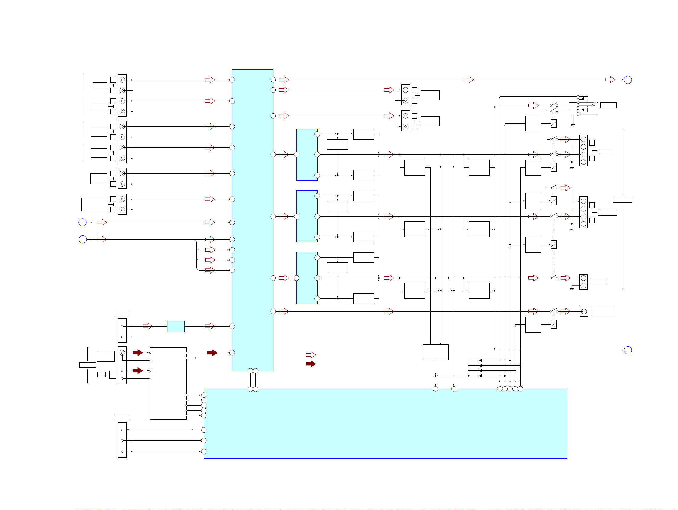
• SIGNAL PATH
: TUNER
: AUDIO (ANALOG)
• R-ch is omitted due to same as L-ch.
A_AUDIO
N
DMPORT
DMPORT
P
XML
VIDEO 1
AUDIO IN
INL13
38
J404 (1/2)
L
R R-CH
FLOUT
14
P_DET
Q
SL
L, C, SW, SL
C
L
SW
R
J401 (2/2)
L
R
SA-CD/CD
CD-R OUT
R-CH
RECL2
27
J404 (2/2)
L
R
VIDEO 1
AUDIO OUT
R-CH
+VOUT1
2
NF1
5
-VOUT1
3
LIMITER
Q701, 702
BOOSTER
Q703
BOOSTER
Q704
CURRENT
DETECT
Q711, 712
IN1
6
POWER AMP
IC700
AF POWER
PROTECT
Q720
RELAY
DRIVE
Q350
RELAY
DRIVE
Q375
PROTECTOR
68
16 17
VACS_CTRL
119
PROTECT
SWITCH
Q320, 321, 325
SLOUT
18
+VOUT1
2
NF1
5
-VOUT1
3
LIMITER
Q801, 802
BOOSTER
Q803
BOOSTER
Q804
CURRENT
DETECT
Q811, 812
IN1
6
POWER AMP
IC800
AF POWER
PROTECT
Q820
COUT
16
+VOUT2
12
NF2
9
-VOUT2
11
LIMITER
Q651, 652
BOOSTER
Q653
BOOSTER
Q654
CURRENT
DETECT
Q661, 662
IN2
8
POWER AMP
IC600
AF POWER
PROTECT
Q670
SWOUT
15
+
−
+
−
RELAY
DRIVE
Q301
RY301
RY355
RY360
RY350
RY375
RELAY
DRIVE
Q360
R-CH
R-CH
+
−
+
−
R-CH
RELAY
DRIVE
Q355
+
−
HP_DETECT
HP_RY
SW RY
C/SUR/SB
12 13
FRONT A RY
14
D1112
D1111
D1108
D1107
J790
PHONES
TB601
L
R
FRONT
TB604
L
R
SURROUND
SPEAKERS
TB607
CENTER
J405
SUB WOOFER
AUDIO OUT
6-4. BLOCK DIAGRAM - AUDIO Section -
(Page 17)
(Page 17)
(Page 15)
(Page 19)
STR-K7200
STR-K7200
1919
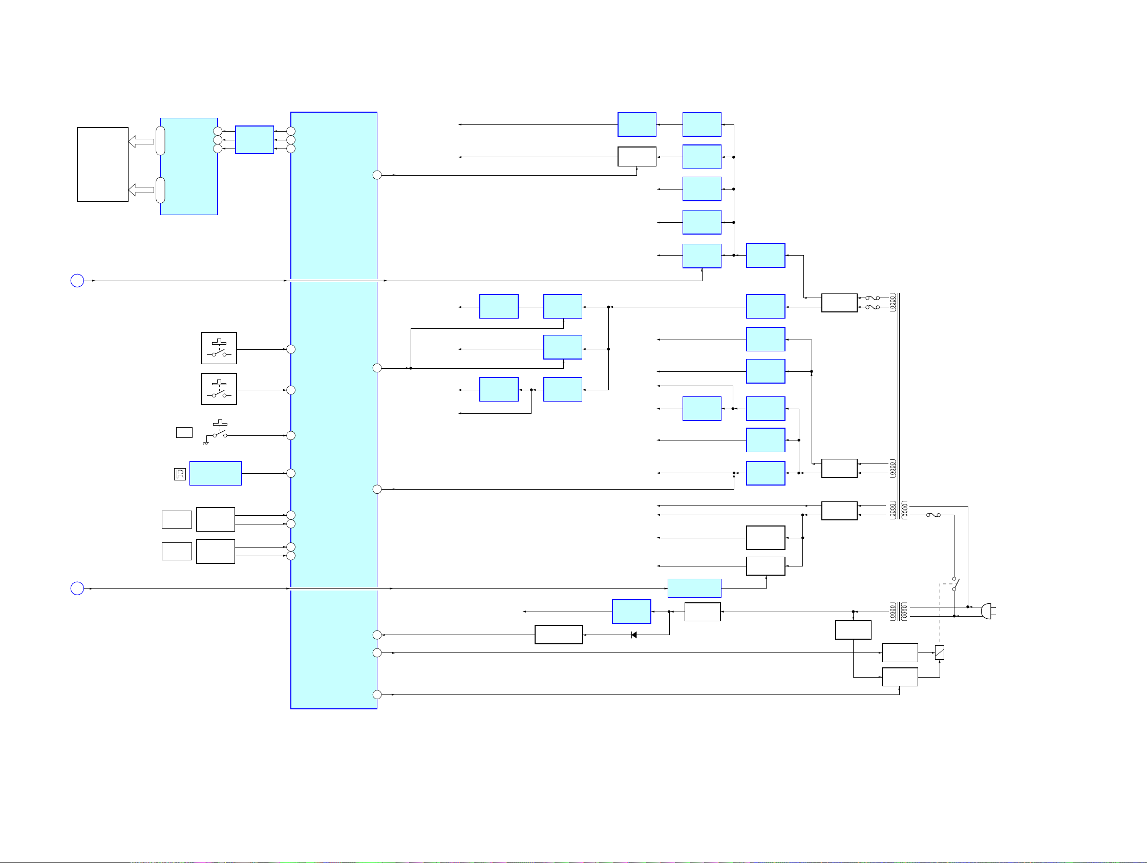
(AC IN)
F901
B+
B-
POWER AMP -45V
FL -20V
TU +9V
VIDEO +5V
DSP +3.3V
DSP +1.2V
HDMI +3.3V
HDMI +1.8V
XM VCC (+5V)
XM +3.3V
HDMI +5V
FL +5V
DMPORT +5V
VIDEO -5V
A-7V
A+5V
A+7V
SYS +3.3V
9
POWER_RY
25FUSE_DETECT
7
86XMDPOWER
HDMI_REG_CTL
SYSTEM CONTROLLER
IC1010 (4/4)
71
FL_DATA
70
FL_CLK
69
FL LAT
FLUORESCENT
INDICATOR TUBE DRIVER
IC100
7
DIN
8
CLK
9
STB
FLUORESCENT
INDICATOR
TUBE
FL101
SEG1 – SEG16,
SEG17
14 – 29, 31
GRID1 – GRID11
42 – 32
84
SIRCS_IN
ROTARY
ENCODER
RV101
LEVEL SHIFT
IC101
REMOTE CONTROL
RECEIVER
IC103
INPUT
SELECTOR
I/
S109 – 112, 115
85
POWER KEY
113
AD_KEY1
S101 – 108
114
AD_KEY2
90
89
INPUT ENCODER A
S100
INPUT ENCODER B
ROTARY
ENCODER
RV102
MASTER
VOLUME
80
79
VOL_JOG (2B)
VOL_JOG (2A)
Q
83STOP
97SUBT
P_DET
K
5VPWR
SUB POWER
TRANSFORMER
T904
RELAY DRIVE
Q901
RECT
D950 – 953
RECT
D910 – 913
RECT
D921
AC OFF DETECT
Q990
RY901
D990, 991
+3.3V
REGULATOR
IC1904
+5V
REGULATOR
IC201
+9V
REGULATOR
IC1902
+4.1V
REGULATOR
IC4100
+3.3V
REGULATOR
IC3527
+1.8V
REGULATOR
IC3528
+1.2V
REGULATOR
IC1002
+3.3V
REGULATOR
IC3526
+3.3V
REGULATOR
IC1013
+6.3V
REGULATOR
IC4001
+7V
REGULATOR
IC350
-20V
REGULATOR
Q930
B- SWITCH
Q500, 501
+5V
REGULATOR
IC1001
+5V
REGULATOR
IC3516
+5V
REGULATOR
IC1031
+5V
REGULATOR
IC1012
+5.5V
REGULATOR
IC106
B+ SWITCH
Q105, 106
+5V
REGULATOR
IC107
+3.3V
REGULATOR
IC101
MAIN POWER
TRANSFORMER
T901
PROTECT DETECT
IC565
RECT
D4001, 4002
-5V
REGULATOR
IC202
-7V
REGULATOR
IC352
F4002
F4001
RECT
D955
B+ SWITCH
Q951, 955
6-5. BLOCK DIAGRAM - POWER SUPPLY Section -
(Page 16)
(Page 18)
STR-K7200
STR-K7200
2020
For Schematic Diagrams.
Note:
• All capacitors are in μF unless otherwise noted. (p: pF)
50 WV or less are not indicated except for electrolytics
and tantalums.
• All resistors are in Ω and 1/4 W or less unless otherwise
specifi ed.
• f : internal component.
• 2 : nonfl ammable resistor.
• 5 : fl usible resistor.
• C : panel designation.
THIS NOTE IS COMMON FOR PRINTED WIRING BOARDS AND SCHEMATIC DIAGRAMS.
(In addition to this, the necessary note is printed in each block.)
• A : B+ Line.
• B : B– Line.
• Voltages and waveforms are dc with respect to ground
under no-signal (detuned) conditions.
no mark : TUNER
• Voltages are taken with a VOM (Input impedance 10 MΩ).
Voltage variations may be noted due to normal production
tolerances.
• Waveforms are taken with a oscilloscope.
V oltage variations may be noted due to normal production
tolerances.
• Circled numbers refer to waveforms.
• Signal path.
J : AUDIO (DIGITAL)
F : AUDIO (ANALOG)
f : TUNER
E : VIDEO
For Printed Wiring Boards.
Note:
• X : Parts extracted from the component side.
• Y : Parts extracted from the conductor side.
• f : Internal component.
• : Pattern from the side which enables seeing.
(The other layers' patterns are not indicated.)
• Indication of transistor.
CEB
These are omitted.
Caution:
Parts face side:
(SIDE A)
Pattern face side:
(SIDE B)
Parts on the parts face side seen from
the pattern face are indicated.
Parts on the pattern face side seen from
the parts face are indicated.
• Circuit Boards Location
Caution:
Pattern face side:
(Conductor Side)
Pattern face side:
(Component Side)
Parts on the pattern face side seen from
the pattern face are indicated.
Parts on the parts face side seen from
the parts face are indicated.
Note: The components identifi ed by mark 0 or dotted
line with mark 0 are critical for safety.
Replace only with part number specifi ed.
C
Q
B
E
These are omitted.
POWER board
DCAC board
HEADPHONE board
VIDEO 2 board
STANDBY board
DISPLAY board
DCDC CONVERTER board
HDMI board
XM board
TUNER (FM/AM)
DIGITAL AB board
MAIN board
VIDEO board
STR-K7200
STR-K7200
2121
E
20
21
41
60
40
61
80
1
E
E
E
D940
R401
D941
R402
D942
R403
D943
R404
R405
R408
R409
R600
Q661
Q662
R602
R605
D375
D761
Q861
R801
Q862
R802
R803
Q670
R804
R805
R806
R807
R808
D770
Q870
D775
R811
R814
R815
R816
R430
R431
R820
R821
R822
R823
R824
C400
C403
C405
R830
R449
R450
R451
R452
R453
R454
R455
C802
R458
C804
R459
R651
R652
R653
R654
R656
R657
R658
C811
R466
R467
R851
R852
R853
C430
R854
C431
R661
R856
R857
R470
R664
R858
R665
R666
C820
R861
R670
R864
R671
R865
R672
R866
R673
R674
R675
R676
C449
R870
R871
R872
R873
C450
R680
R874
Q301
R880
C652
C654
Q501
C852
C854
C661
JR406
Q320
JR605
C861
Q321
JR606
JR607
C670
Q325
C675
Q711
Q712
C870
D811
C489
Q720
D820
C499
JR434
JR435
Q350
Q355
Q360
R301
R304
R501
R502
R503
R504
R505
R506
R507
D661
Q375
Q761
R701
Q762
R702
R703
R704
R705
R706
R707
R320
R708
D861
D670
R325
R326
R327
Q770
R328
D675
R711
R714
R715
R716
D870
R335
R336
R337
R720
R721
R722
R723
R724
R725
R726
CL001
CL003
R730
C500
R350
R353
R930
R931
R355
C702
R358
C704
R360
C900
R363
C711
R751
R752
R753
R754
R756
R757
R758
C720
R375
R378
R761
C725
R764
R765
R766
R770
R771
R772
R773
R774
C350
R775
R776
C352
C933
R780
D301
C940
C941
C752
C754
D500
D501
E
E
C761
D320
JR702
D325
D326
D327
C770
JR320
JR321
D711
JR322
C775
Q811
C3022
Q812
C3025
C3026
C3027
D335
D720
Q820
D725
C3032
C3037
R3010
R3011
R3012
R3013
5
8
1
4
JR340
D350
D352
R3020
D930
R3021
D355
D931
R3022
R3023
D360
5
8
1
4
E
E
E
E
E
E
E
E
E
E
E
E
E
E
E
E
E
E
EB
2
15
1
6
EB
2
14
1
15
2
14
1
15
1
13
1
15
EB
143
173
E
B
153
2
14
1
15
1
3
EB
BECBECBECBE
C
BECBECBECBECBECBE
C
3
213
3
1
1
3
1
3
1
7
1
1
6
3
E
B
E
BEB
EB EBE
B
E
B
Q654
JW758
TB601
CNP912
JW760
Q851
JW761
Q852
JW762
Q853 Q854
HS350
IC350
IC352
JW766
JW767
JW768
JW769
CNP921
JW770
JW771
JW772
JW773
JW776
JW777
R809
JW779
CNP930
R810
JW781
R812
JW782
R813
JW783
JS710
JS711
JW785
JS712
JW789
CNP940
L678
JW790
JS335
JW791
JS336
JS337
JS338
JW794
JS339
JW795
R828
JW798
R829
JW799
L878
C408
C409
JS920
JS922
JWH1
JWH2
JWH3
CN434
JWH4
JWH5
JWH7
JWH9
C801
C803
JS930
C805
C806
C807
C808
C809
R659
R660
R662
R663
JS3001
R859
JS3002
C821
R860
R862
R863
C829
R678
R679
R487
JS578
R488
JS388
C644
JS389
R878
R879
JS3022
JS778
C458
C459
JS392
JS393
JS394
C844
C651
C653
JW600
C655
JW601
C656
JW602
C657
JW603
C658
JW604
Q500
C659
JW605JW606
JW607
JW608
C851
JW609
JS3037
C853
JW800
C855
JW801
C856
JW802
C857
JW803
C858
JW610
JW804
C471
C859
Q701
JW611
Q702
JW612
Q703
JW613
JW807
Q704
JW614
JW615JW616
JW617
JW618
JW619
C671
JW813
JW620
JW814
JW621
JW815
JW622
JW816
JW623
JW817
C679
JW819
JW626
C487
JW627
C488
C871
JW629
IC600
TB604
TB607
JW630
C879
JW631
JW825
JW632
JW826
JW633
JW827
JW634
JW635
JW829
JW636
JW637
IC800
JW638
JW639
JW830
JW831
JW832
JW833
JW640
JW834
JW641
JW835
JW642
JW836
JW643
JW837
JW644
CNP410
JW838
JW645
CNP411
JW839
JW646
JW647
JW648
L728
Q930
JW840
JW841
JW842
JW843
JW650
JW651
JW845
JW652
JW846
JW653
JW655
JW656
JW657
JW658
JW659
R302
R303
JW852
JW660
Q751
JW661
JW855
Q752
Q753
CNP430
Q754
JW664
JW859
JW665
JW667
JS400
JS401
JS402
JW860
JW861
JW862
JW863
JS408
JW864
JW670
JS409
JW671
JW866
JW672
JW867
JW868
R510
R511
JW675
JW676
JW677
JS410
JS411
R709
JW679
JWH10
JW870
JWH11
JW871
JWH12
JW872
R710
CN500
JW681
R712
R713
JW684
JS611
JW685
JW686
JW687
JW688
JW689
JS810
JW690
JW691
JW692
JW693
JW694
JW695
JW696
R728
R729
JW699
JS432
JS628
L778
R545
R351
R546
R352
C701
R356
R932
C703
R357
C705
C706
C707
C320
C708
C709
R361
C325
R362
C904
R940
JS458
JS459
CN350
JS460
JS461
R759
C335
C721
R376
R377
R760
R762
R763
C729
RY301
JS470
C920
CN941
JS471
C921
JS472
C922
JS473
C923
C351
C545
C546
C353
R778
C930
R779
C931
R392
C932
R393
C744
C751
C753
JW700
C755
C756
C757
C758
JW704
C759
JW705
JW706
JW707
JW708
JW321
JW709
JW322
JW323
JW324
JW325
JW326
JW327
JW328
JW710
JW329
Q801
Q802
JW712
Q803
JW713
Q804
JW714
JW715
JW716
JW717
JW330
JW718
JW331
JW332
C771
CN792
JW720
JW721
C3024
RY350
C779
RY355
IC700
W001
ET902
W002
JW731
RY360
C3034
CNP500
JW737
JW738
D921
JW739
JW740
JW741
JW743
JW745
JW746
JW747
JW748
RY375
JW749
L828
JW750
JW751
JW752
JW753JW754
Q651
JW755
Q652
JW756
Q653
J401 J403 J404
J405
IC3002
IC565
IC400
MAIN BOARD
1-875-588-
D
XM BOARD
CN102
H
DCAC
BOARD
CN2000
C
VIDEO 2
BOARD
CNP201
B
A
DIGITAL
AB
BOARD
CNS502
DIGITAL
AB
BOARD
CNS501
J
MAIN POWER
TRANSFORMER
T901
MAIN POWER
TRANSFORMER
T901
L
DIGITAL
AB
BOARD
CNP505
K
STANDBY BOARD
CN912
E
HEADPHONE
BOARD
CNP790
M
DISPLAY
BOARD
CN108
N
G
VIDEO
BOARD
CNP203
F
DIGITAL
AB BOARD
CNP504
LR
TV
IN
LR
SA-CD/CD/
CD-R
IN
LR
SA-CD/CD/
CD-R
OUT
LR
SAT
AUDIO IN
LR
DVD
AUDIO IN
LR
VIDEO 1
AUDIO OUT
LR
VIDEO 1
AUDIO IN
SUB WOOFER
AUDIO OUT
CENTER
SURROUND
RL
FRONT
SPEAKERS
LR
RY350, 355
RY360, 375
-1
-2
RY301
12
(12)
(CHASSIS)
(CHASSIS) (CHASSIS) (CHASSIS) (CHASSIS)
A
B
C
D
E
F
G
H
1 2 3 4 5 6 7 8 9 10 11 12 13 14
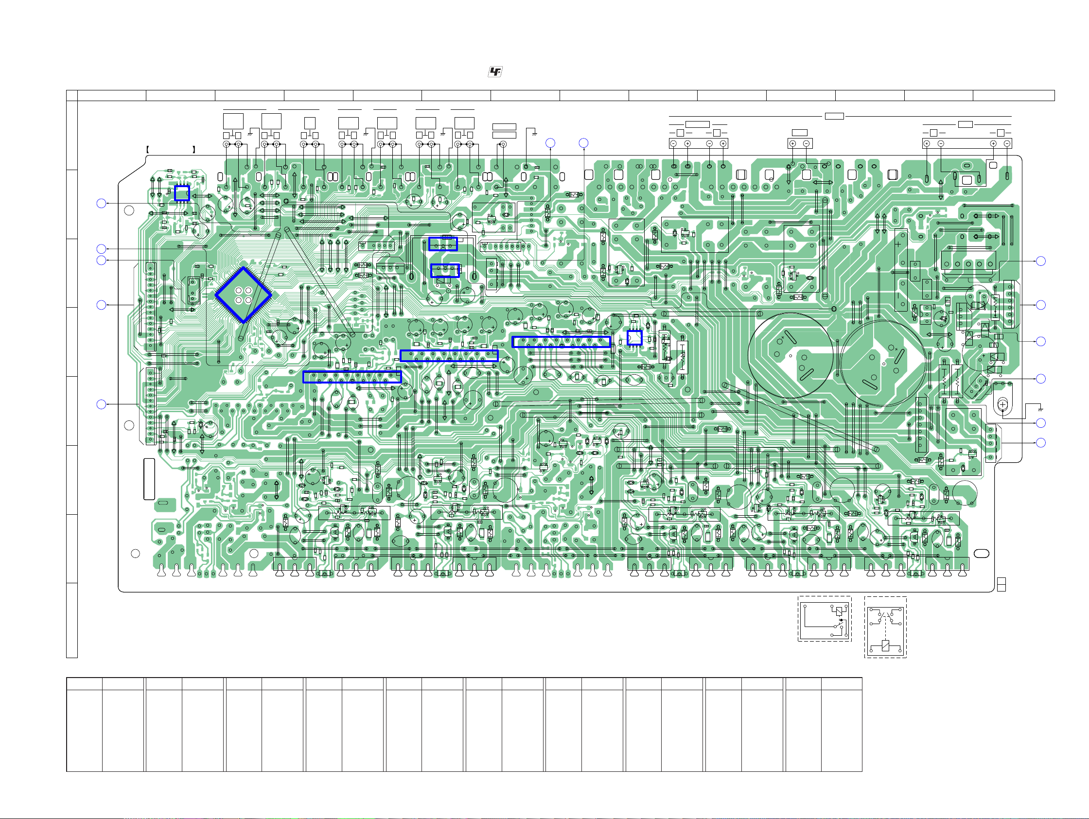
6-6. PRINTED WIRING BOARD - MAIN Board -
• : Uses unleaded solder.
• See page 20 for Circuit Boards Location.
Ref. No. Location Ref. No. Location Ref. No. Location Ref. No. Location Ref. No. Location Ref. No. Location
• Semiconductor Location
Ref. No. Location Ref. No. Location Ref. No. Location Ref. No. Location
D301 B-7
D320 F-8
D325 F-8
D326 E-8
D327 E-8
D335 E-2
D350 C-11
D352 C-6
D355 B-9
D360 C-8
D375 F-13
D500 D-9
D501 D-9
D661 F-4
D670 F-4
D675 F-4
D711 F-9
D720 F-9
D725 F-9
D761 F-6
D770 F-6
D775 F-6
D811 F-12
D820 F-13
D861 F-11
D870 F-11
D921 C-12
D930 C-14
D931 D-13
D940 D-14
D941 D-14
D942 D-13
D943 D-14
IC350 C-6
IC352 C-6
IC400 C-3
IC565 D-9
IC600 E-4
IC700 D-6
IC800 D-7
IC3002 B-2
Q301 B-7
Q320 E-8
Q321 F-7
Q325 E-8
Q350 C-11
Q355 B-9
Q360 C-8
Q375 F-13
Q500 E-9
Q501 D-9
Q651 G-4
Q652 G-4
Q653 G-4
Q654 G-5
Q661 F-5
Q662 F-4
Q670 F-4
Q701 G-9
Q702 G-9
Q703 G-9
Q704 G-10
Q711 F-10
Q712 F-9
Q720 F-9
Q751 G-6
Q752 G-6
Q753 G-5
Q754 G-6
Q761 F-6
Q762 F-6
Q770 F-6
Q801 G-13
Q802 G-13
Q803 G-12
Q804 G-13
Q811 G-13
Q812 G-13
Q820 F-12
Q851 G-11
Q852 G-11
Q853 G-11
Q854 G-11
Q861 F-11
Q862 F-11
Q870 F-10
Q930 D-13
(Page 32)
(Page 34)
(Page 40)
(Page 31)
(Page 31)
(Page 31)
(Page 40)
(Page 46)
(Page 46)
(Page 42)
(Page
31)
(Page
46)
(Page 34)
STR-K7200
STR-K7200
2222
• See page 48 for IC Block Diagrams.
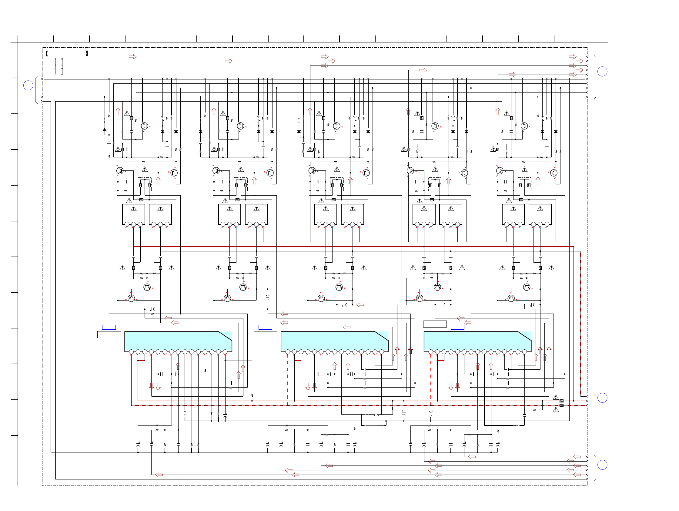
6-7. SCHEMATIC DIAGRAM - MAIN Board (1/3) -
BOARD
MAIN
(2/3)
1
BOARD
MAIN
(2/3)
4
2
BOARD
(3/3)
MAIN
3
(3/3)
BOARD
MAIN
IC B/DIC B/DIC B/D
2.8
1.1
-1.1
-43.2
0.1
0.1
0.1
0.1
-43.2
-1.1
1.1
44.8
-44.8
1.1
0.1
1.1
0.1
-43.2
0.1
2.8
0.1
44.8
-44.8
-43.2
-1.1
-1.1
1.1
0
0
0.1
-43.1
0.1
2.8
0
44.8
-44.8
-44.8
0
-1.1
0
0
0
0
-0.6
-1.1
0.5
1.1 -1. 1
0.5
1.1
-0.6
-1.1
-1.1
0.5
1.1
-0.6
-1.1
-1.1
1.1
0.5
-1.1
-1.1
-0.6
1.1
0.5
-1.1
-1.1
-0.6
-44.8
0
-1.1
44.8
0
1.1
-44.8
-1.1
0
1.1
0
44.8
-44.8
-1.1
0
1.1
0
44.8
-44.8
-1.1
0
1.1
0
44.8
-44.8
-1.1
0
1.1
0
44.8
0
-43.8-43.8
0
0
-43.8
0
0
-43.8
0
0
-43.8
0
0
0
0
0
0
0
0
0
0
0
0
0
0
0
4.14.1
0
4.1
0
4.1
0
4.1
0
560
R658
15kR672
500V
C658
47p
123
MN2488-OPY-MK
Q653
BCE
6.2k
R662
47kR680
2.2k
R656
100kR676
2SA1163L-TE85L
Q662
1.5kR664
2SA1115TP-EF
Q651
50V
10
C671
0.022
C679
82k
R657
4.7kR661
2SA1163L-TE85L
Q661
68kR666
2SC3052EF-T1-LEF
Q670
25V
47
C657
10
R679
123
MP1620-OPY-MK
Q654
BCE
L678
15kR665
0.22
R663
0.01
C670
220p
C661
2SC3623ATP-LK
Q652
500V
47p
C659
4.7
R678
2SA1163L-TE85L
Q711
560
R808
0.22
R813
123
MN2488-OPY-MK
Q803
BCE
47k
R830
0.22
R863
500V
C758
47p
2SA1163L-TE85L
Q862
2SA1115TP-EF
Q701
123
MN2488-OPY-MK
Q753
BCE
25V47C807
4.7kR811
47k
R780
82k
R857
2SA1115TP-EF
Q801
100k
R776
68kR854
2SA1163L-TE85L
Q762
1.5kR764
2SC3623ATP-LK
Q702
4.7kR861
1.5k
R714
100p
C804
500V
C708
47p
0.01C870
560
R708
50V
10
C771
123
MP1620-OPY-MK
Q804
BCE
220p
C711
4.7k
R761
500V3p
C805
25V
47
C857
68kR766
2SC3052EF-T1-LEF
Q770
68kR704
1.5k
R814
R805
22k
25V
47
C757
123
MN2488-OPY-MK
Q703
BCE
10
R779
10
R729
L878
15kR815
500V3p
C855
123
MP1620-OPY-MK
Q754
BCE
15kR822
2SA1163L-TE85L
Q712
2.2k
R706
500V
C858
47p
2SC3052EF-T1-LEF
Q720
0.01C720
1.5kR864
R705
22k
100p
C704
220p
C761
2SC3623ATP-LK
Q752
100p
C754
4.7
R778
560
R758
500V
47p
C709
0.01C820
15kR772
2SA1163L-TE85L
Q811
2SC3623ATP-LK
Q802
68kR754
100p
C854
2.2k
R856
0.022
C879
500V
47p
C809
2SA1163L-TE85L
Q812
2.2k
R756
68kR804
50V10C721
L828
123
MP1620-OPY-MK
Q854
BCE
220p
C861
500V
3p
C705
25V47C707
68kR816
2SA1115TP-EF
Q851
2SA1115TP-EF
Q751
50V10C821
10
R879
82k
R707
L728
2.2k
R806
15kR722
4.7kR711
10
R829
500V
C808
47p
0.022
C779
2SA1163L-TE85L
Q861
82k
R757
560
R858
4.7
R728
0.022
C729
2SA1163L-TE85L
Q761
123
MP1620-OPY-MK
Q704
BCE
6.2kR862
500V
47p
C859
15kR865
2SC3052EF-T1-LEF
Q870
15kR872
68kR866
47k
R880
15kR715
L778
4.7
R878
6.2kR812
15kR765
2SC3623ATP-LK
Q852
0.22
R763
0.01
C770
0.22
R713
0.01
C775
6.2k
R712
82k
R807
500V3p
C755
50V10C871
123
MN2488-OPY-MK
Q853
BCE
0.022
C829
68kR716
4.7
R828
220p
C811
500V
47p
C759
2SC3052EF-T1-LEF
Q820
115 14 13 12 11 10
uPC2581V-S
IC700
115 14 13 12 11 10
uPC2581V- S
IC800
100V
10
C546
1
R546
1
R545
100V
10
C545
500V
3p
C655
100p
C654
50V
C651
10
R605
22k
1k
R651
100p
C652
68kR654
68k
R652
1k
R751
1kR701
50V
C751
10
100p
C752
100p
C702
50V
C701
10
68k
R752
68k
R702
1k
R851
1k
R801
50V
C851
10
100p
C852
100p
C802
50V
C801
10
68k
R852
68k
R802
R730
47k
MA2J1110GLS0D661
MA2J1110GLS0
D675
MA2J1110GLS0D870
MA2J1110GLS0D820
MA2J1110GLS0D861
MA2J1110GLS0
D670
MA2J1110GLS0D811
MA2J1110GLS0D761
MA2J1110GLS0
D770
MA2J1110GLS0D720
MA2J1110GLS0
D775
MA2J1110GLS0D711
MA2J1110GLS0
D725
100k
R726
0.01
C725
0JR605
0JR606
22kR720
22kR670
22kR870
22kR770
22kR820
50V
C644
10
50V
C844
10
50V
C744
10
JR607
0
JS628
3.3kR771
3.3kR821
3.3kR871
22kR824
22kR674
22kR724
22kR874
22kR774
22kR773
22k
R873
22kR723
22kR673
22kR823
100
R760
100
R859
100
R709
100
R809
100
R810
100
R860
100
R710
100
R660
100
R659
100
R759
2.2kR853
2.2k
R703
2.2k
R803
2.2kR753
2.2kR653
JS712
JS710
JS611
JS810
JS711
6.2k
R762
JS337
JS339
JS338
0
R600
0
R602
500V
33p
C853
500V
33p
C803
500V
33p
C653
500V
33p
C703
500V
33p
C753
10V
C706
220
10V
C756
220
10V
C856
220
10V
C656
220
10V
C806
220
JR340 0
JS578
3.3kR671
3.3kR721
10k
R675
10k
R725
10k
R775
0.01
C675
151413121110987654321
uPC2581V-S
IC600
MUTE
+VOUT1
-VOUT1
COMP1
NF1
IN1
GND
IN2
NF2
COMP2
-VOUT2
+VOUT2
VCC
VCC
VEE
MUTE
+VOUT1
-VOUT1
COMP1
NF1
IN1
GND
IN2
NF2
COMP2
-VOUT2
+VOUT2
VCC
VCC
VEE
MUTE
+VOUT1
-VOUT1
COMP1
NF1
IN1
GND
IN2
NF2
COMP2
-VOUT2
+VOUT2
VCC
VCC
VEE
98765432 98765432
13
15
17
18
19
20
21
22
23
242
1
3
11
12
4
6
9
10
25
26
27
(1/3)MAIN BOARD
POWER AMP
IC800
POWER AMP
IC700
POWER AMP
IC600
BOOSTERBOOSTERBOOSTER BOOSTERBOOSTER BOOSTERBOOSTER BOOSTERBOOSTER BOOSTER
Q651, 652
LIMITER
Q751, 752
LIMITER
Q701, 702
LIMITER
Q851, 852
LIMITER
Q801, 802
LIMITER
Q811, 812
CURRENT
DETECT
AF POWER
PROTECT
DETECT
CURRENT
Q861, 862
DETECT
CURRENT
Q711, 712
DETECT
CURRENT
Q761, 762
DETECT
CURRENT
Q661, 662
PROTECT
AF POWER
PROTECT
AF POWER
PROTECT
AF POWER
PROTECT
AF POWER
D
B
1610 11
F
5 15
L
K
3
G
1 12
C
E
H
8967
J
4 13
A
142
I
(Page
23)
(Page 24)
(Page 24)
(Page 23)
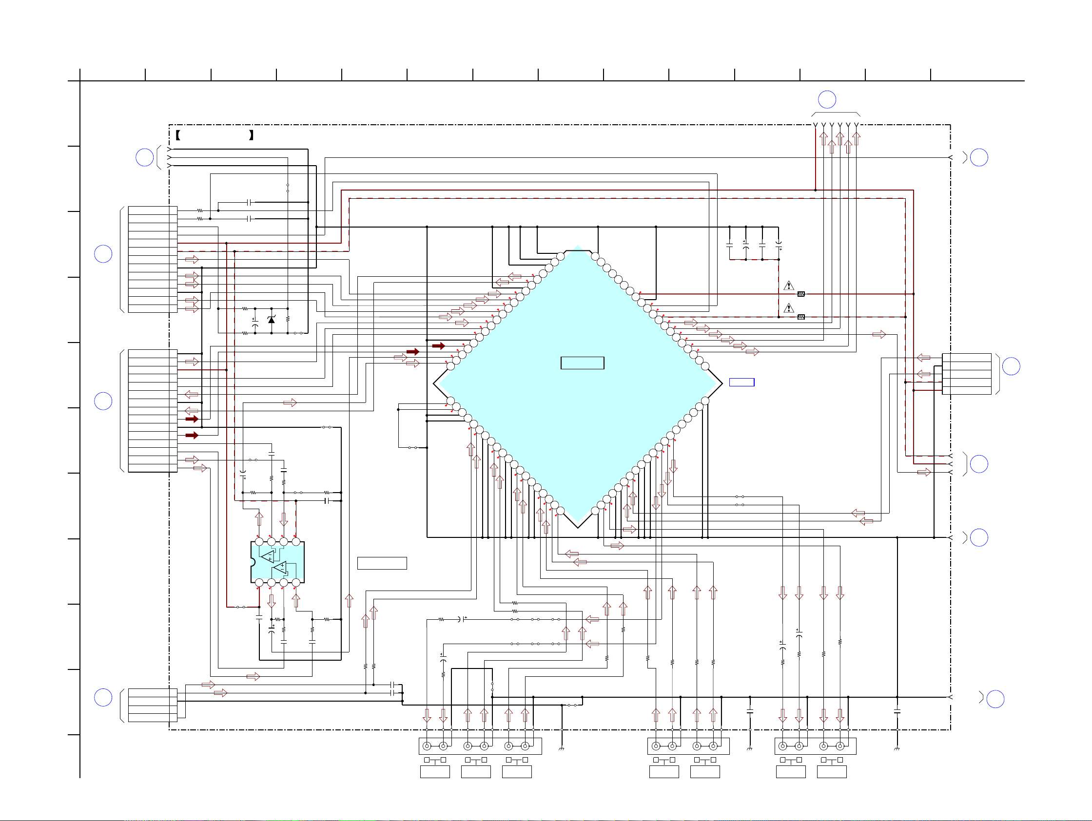
STR-K7200
STR-K7200
2323
• See page 48 for IC Block Diagrams.
6-8. SCHEMATIC DIAGRAM - MAIN Board (2/3) -
XM
D
BOARD
CN102
(2/5)
DIGITAL
AB BOARD
CNS502
A
C
VIDEO 2
CNP201
BOARD
(1/3)
BOARD
MAIN
4
MAIN
BOARD
(3/3)
5
BOARD
MAIN
6
(3/3)
BOARD
MAIN
7
(3/3)
BOARD
(3/3)
8
MAIN
MAIN
BOARD
(1/3)
1
B
CNS501
(2/5)
AB BOARD
DIGITAL
IC B/D
7
0
0
0
0
0
0
-6.9
0
0
-6.9
0
0
0
0
0
0
7
0
0
0
0
0
0
0
0
0
0
0
0
0
0
0
0
0
0
0
0
0
0
0
0
0
0
0
0
0
0
0
0
0
R3010
47k
R3011
47k
C3037
1
C3032
1
C3027
1
R3012
47k
R3013
47k
R3021 47k
R3022
47k
50V
C3024
4.7
50V
C3034
4.7
C3025
0.1
C3022
1
R3020 47k
C3026
0.1
8765
1234
NJM4565M(TE2)
IC3002
50V
C409
4.7
R451
1k
50V
C459
4.7
R402
1k
R459
1k
R409
1k
R401
1k
R452
1k
J401
6P
R453
1k
R403
1k
R454
1k
R404
1k
C403
2200p
R405
1k
50V
C458
4.7
R455
1k
R408
1k
50V
C408
4.7
R458
1k
C405
2200p
6.8k
R335
0.1
C489
100p
C449
0.1
C499
100p
C450
C430 220p
C431
220p
MAZ8030G0LS0
D335
1
2
3
4
5
6
7
8
9
10
11
12
13
14
15
16
17
18
19
20
21
22
23
24
25
26
27
28
29
30
31
32
33
34
35
36
37
38
39
4041
42
43
44
45
46
47
48
49
50
51
52
53
54
55
56
57
58
59
60
61
62
63
64
65
66
67
68
69
70
71
72
73
74
75
76
77
78
79
80
BD3471KS2
IC400
GND
HPFN
LPF01
LPF02
LPFN2
LPFN1
SWVOL
VCC
DGND
DATA
CLK
VEE
FROUT
FLOUT
SWOUT
COUT
SROUT
SLOUT
SBROUT
SBLOUT
GND
GND
RECL4
RECR4
RECL3
RECR3
RECL2
RECR2
RECL1
RECR1
GND
INL16
INR16
INL15
INR15
INL14
INR1
INL1
INR13
GND
INL12
INR12
INL11
INR11
INL10
INR10
INL9
INR9
INL8
INR8
INL7
INR7
INL6
INR6
INL5
INR5
INL4
INR4
INL3 (DCAC_MIC)
INR3 (DCAC_MIC)
INL2 (DMPORT_L)
INR2 (DMPORT_R)
INL1 (TUNER_L)
INR1 (TUNER_R)
GND
SBLIN
SBRIN
SLIN
SRIN
CIN
SWIN
LIN
RIN
GND
ROUT
LOUT
GND
ROUT SUB
LOUT SUB
GND
1
2
3
4
5
6
7
8
9
10
11
12
13
13P
CNP410
VOL IC CLK
VOL IC DATA
VACS CTRL
PROTECTOR
+7V
-7V
FR OUT
AGND
FL OUT
SW
AGND
C OUT
SR OUT
1
2
3
4
5
6
7
8
9
10
11
12
13
14
15
15P
CNP411
AGND
SL OUT
+7V
SBR OUT
SBL OUT
L IN
AGND
R IN
TUNER R
AGND
TUNER L
DMPORT LDMPORT RDMPORT L+
DMPORT R+
R3023
47k
1
3
4
CNP430
4P
L-CH
2
NC
GND
R-CH
R430
1k
R431
1k
JS335
JS409
JS410
JS411
JS461
JS459
JS460
JS400
1kR449
1k
R450
JS408
JS458
JS3002
JS3037
JS3022
JS3001
JS336
J403
4P
J404
4P
JS401
1
3
4
5
6
6P
CN434
XMR
XMGND
XML
-7V
+7V
JS432
R487
2.2
R488
2.2
25V
C487
47
25V
C488
47
0
R336
22k
R337
16V
47
C335
28
29
30
31
32
964121110
3
1
2
MAIN BOARD (2/3)
BUFFER
IC3002
IC400
ANALOG SOUND PROCESSOR
W001-002
VEE
VCC
(CHASSIS) (CHASSIS) (CHASSIS)
LR
CD-R OUT
SA-CD/CD/
LR
SA-CD/CD/
CD-R IN
LR
TV IN
LR
SAT AUDIO
IN
LR
DVD AUDI O
IN
LR
VIDEO 1
AUDIO OUT
LR
VIDEO 1
AUDIO IN
D
B
10 11
F
5
K
3
G
1 12
C
E
H
8967
J
4 13
A
142
I
INPUT SELECTOR,
ELECTRICAL VOLUME
(Page 22)
(Page 26)
(Page 26)
(Page 41)
(Page 22)
(Page 24)
(Page 33)
(Page 24)
(Page 24)
(Page 24)
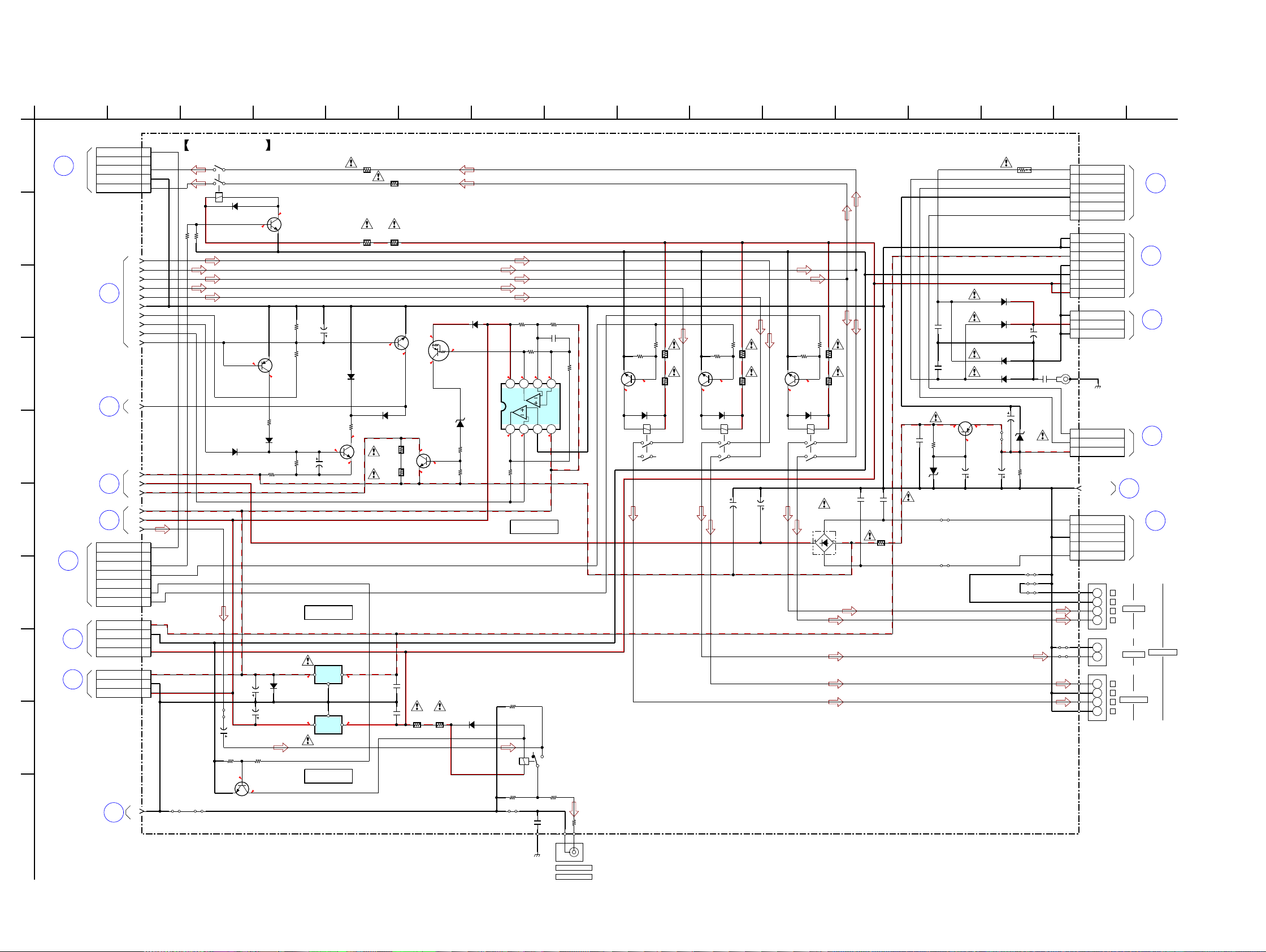
STR-K7200
STR-K7200
2424
6-9. SCHEMATIC DIAGRAM - MAIN Board (3/3) -
8
TRANSFORMER
T901
MAIN POWER
J
STANDBY
CN912
K
BOARD
CNP505
DIGITAL
(4/5)
L
AB BOARD
DISPLAY
CN108
M
BOARD
BOARD
(2/3)
MAIN
N
MAIN POWER
T901
TRANSFORMER
E
CNP790
BOARD
HEADPHONE
2
(1/3)
BOARD
MAIN
BOARD
(2/3)
MAIN
5
MAIN
(1/3)
BOARD
3
MAIN
(2/3)
BOARD
6
CNP504
F
(4/5)
AB BOARD
DIGITAL
BOARD
G
VIDEO
CNP203
CN2000
BOARD
DCAC
H
BOARD
(2/3)
7
MAIN
167
-16.8-6.9
-19.8
-20.4
-44.8
0.8
0.20.2
0.8
0.2
0.8
6.4
-43.8
-5.5
6.4
3.3
0
0
16
-44.8
-44.8
3.2
0
-44.3
-44.8
-44.8
0.1
0.7
-5.5
-5.
7
5
-3.6
-5.5
1.2
-6.9
C400
2200p
R466
1k
R470
47k
RY301
2SC3052EF-T1-LEF
Q301
50V
C471
4.7
R467
100k
100V
0.22
C920
100V
0.22
C921
39k
R326
50V
10
C325
10k
R327
6.8k
R325
2SC3052EF-T1-LEF
Q325
2SA1163L-TE85L
Q320
2SC3052EF-T1-LEF
Q321
1k
R328
10k
R503
220k
R507
2SC1815GR-TPE2
Q500
10k
R504
8765
4321
NJM4565M(TE2)
IC565
470k
R502
10k
R505
0.1
C500
2SB734-T-34
Q930
100V
0.1
C933
35V
47
C931
4.7
R932
22k
R930
PTZ-TE25-5.6B
D930
10k
R931
35V
47
C932
1SR154-400TE-25
D352
0.47
C350
0.47
C352
1SR154-400TE-25
D943
0.47
C940
16V
3300
C904
0.47
C941
1SR154-400TE-25
D941
1SR154-400TE-25
D940
1SR154-400TE-25
D942
E
ET902
1
3
4
4P
CN500
+15V
GND
2
NC
-15V
2.2k
R375
2SC3052EF-T1-LEF
Q375
RY375
1
3
4
5
5P
CN792
HP_DETECT
2
NC
R-CH
GND
L-CH
2SC3052EF-T1-LEF
Q360
RY360
12V
2SC3052EF-T1-LEF
Q355
RY355
12V
RY350
12V
2SC3052EF-T1-LEF
Q350
2.2k
R350
RT1P241C-TP- 1
Q501
1k
R355
1k
R360
R301
2.2k
MA2J1110GLS0
D360
MA2J1110GLS0
D326
MA2J1110GLS0
D501
MA2J1110GLS0
D350
MA2J1110GLS0
D325
MA2J1110GLS0
D355
MA2J1110GLS0
D375
MA2J1110GLS0
D320
MA2J1110GLS0
D327
MA2J1110GLS0
D301
JS922
JS920
1
2
3
4
5
6
6P
CNP940
F1
NC
GND
F2
R4 -AC
R4 +AC
1
3
5
5P
CNP921
R1 (UPPER TAP)
2
NC
4
NC
R1 GND
R1 (UPPER TAP)
1
2
3
3P
CNP500
+7V
GND
-7V
MAZ8200GMLS0
D931
47
R362
33
R361
47
R357
33
R356
47
R352
33
R351
47
R37733R376
R302
100
R303
100
D5SBA20-4003
D921
~
~
C923
6800
71V
C922
6800
71V
0
JR320
2W680
R393
2W
R392
680
1
3
4
5
6
7
7P
CN350
HP_DETECT
HP RY
2
NC
C/SUR/SB_RY
FRONT B RY (NC)
SW PREOUT RY
FRONT A RY
2W
R510
330
MAZ8220GMLS0
D500
22k
R501
33k
R506
JS470
JS471
JS472
JS473
JS393
JS394
JS392
JR406
0
2W
100
R511
G
TA7807S
IC350
1
2
3
IIO
O
G
TA79007SB
IC352
1
2
3
47k
R358
47k
R363
47k
R353
47k
R304
47kR378
1
2
3
3P
CNP930
-20V
F1
F2
JS388
JS389
J405
1
2
3
4
5
6
7
7P
CNP912
R2 RETURN GND
NC
-15V
STBY GND
R2 GND IN
+15V
+15V (NC)
1
2
3
3P
CN941
GND (R4)
+7V (R4)
GND (R4) (NC)
JS930
35V
47
C930
10V
220
C320
100k
R320
C900
0.1
1/2W
0.15
R940
16V
100
C353
16V
100
C351
21
23
24
18
13
22
15
20
19
17
25
26
27
28
29
30
31
32
MAIN BOARD (3/3)
PROTECT DETECT
IC565
+7V REGULATOR
IC350
-7V REGULATOR
IC352
(CHASSIS)
AUDIO OUT
SUB WOOFER
B- SWITCH
B- SWITCH
LIMITER
PROTECT SWITCH
PROTECT SWITCH
RELAY DRIVE
VCC
VEE
RELAY DRIVE
RELAY DRIVE
RELAY DRIVE
-2
-1
-2
-1
-2
-1
-1
-2
(CHASSIS)
-20V REGULATOR
W001-002
+
+
-
R
L
L
R
CENTER
+
-
TB607
SURROUND
TB604
+
-
R
FRONT
-
L
+
R
L
TB601
SPEAKERS
RELAY DRIVE
D
B
1610 11
F
5 153
G
1 12
C
E
H
8967
J
4 13
A
142
I
(Page 35)
(Page 22)
(Page 23)
(Page 22)
(Page 23)
(Page 28)
(Page
41)
(Page 35)
(Page 23)
(Page 47)
(Page 47)
(Page 28)
(Page 43)
(Page 23)
(Page 47)
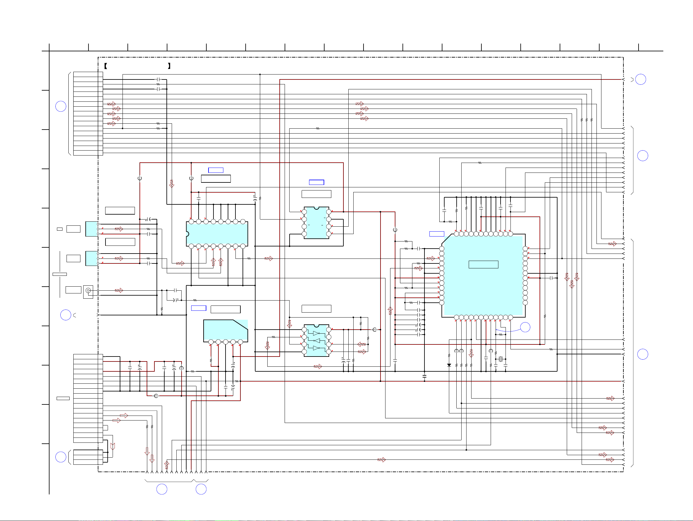
STR-K7200
STR-K7200
2525
• See page 35 for Waveforms. • See page 48 for IC Block Diagrams.
6-10. SCHEMATIC DIAGRAM - DIGITAL AB Board (1/5) -
AB BOARD
DIGITAL
(4/5)
13
DIGITAL
AB BOARD
14
(5/5)
AB BOARD
DIGITAL
(3/5)
15
IC B/D
IC B/D
IC B/D
AB BOARD
DIGITAL
(4/5)
22
IC B/D
1
(5/5)
DIGITAL
AB BOARD
12
(2/5)
DIGITAL
AB BOARD
11
CN3511
(2/2)
BOARD
V
HDMI
CNP242
BOARD
Q
VIDEO
3.2
3.2
0
3.3
3.300
0
2.6
3.3
1.5
2.9
2.9
3.3
1.7
1.6
1.603.3
3.3
1.6
1.6
1.7
0
0
3.3
3.3
3.3
5
5
6.3
3.3
0
2.2
0.1
0.1
0
3.3
1.5
3.3
0
3.3
3.3
0
0.1
3.3
0.1
3.3
2.6
1.7
3.3
1.5
1.5
VCC
OUT
GND
TORX147L
IC1351
1
3
2
100R1354
4.7k
R1302
VCC
OUT
GND
TORX147L
IC1352
1
3
2
470
R1356
0.01C1304
16V
100
C1009
R1940
0
0
R1019
25V
47
C1370
0.1
C1114
1
2
3
4
5
6
7
8
9
10
11
12
13
14
15
16
17
18
18P
J1302
P GND
VBUS +5V
NC
VIDEO 5V
C LINK_RX
C LINK_TX
DET
DGND
WM DET
WM AD
LRL+
R+
WM RxD
WM TxD
DMPORT_VIDEO
VGND(NC)
10V100
C1008
100R1351
0R1139
16V
100
C1923
100
R1359
0.1
C1012
100R1063
0
JR1005
100
R1304
R1358
470k
680k
R1362
100
R1324
4
3
2
1
TC7WH157FK(TE85R)
IC1017
A
B
Y
GND
Y
A/B
C
VCC
FB1350
100
R1041
0.1
C1358
50V
22
C1355
75
R1355
0.1
C1361
5.6k
R1301
12345
IC SI-3050KM-TL
IC1012
VC
VIN
GND
VOUT
SENSE
J1301
0
R1353
33kR1303
0R1368
R1352
0
6.3V
1000
C1359
0.1
C1007
220R1133
22kR1147
0.1
C1354
0.1
C1351
FB1309
4
3
2
1
5
6
7
8
5
6
7
8
TC7WU04FU(TE12R)
IC1303
IN1
OUT3
IN2
GND
OUT2
IN3
OUT1
VCC
47k
R1357
0.1C1303
FB1117
50V
22
C1006
0.1
C1089
FB1310
0.01
C1302
FB1103
100
R1130
10k
R1323
FB1305
18p
C1310
0.1C1305
0.1C1301
13 14 15 16 17 18 19 20 21 22 23 24
25
26
27
28
29
30
31
32
33
34
35
36
12
11
10
9
8
7
6
5
4
3
2
1
373839404142434445464748
IC1301
LC89056W-E
DISEL
DOUT
DINO
DIN1
DIN2
DGND
DVDD
R
VIN_AGND
LPF
AVDD
AGND
CKOUT
BCK
LRCK
DATAO
XSTATE
DGND
DVDD
XMCK
XOUT
XIN
EMPHA
AUDIO
CSFLAG
F0/P0/C0_F0/FSB0
F1/P1/C1_F1/FSB1
F2/P2/C2_F2/DLMP
F3/P3/C3_VF/DATA02
DVDD
DGND
AUTO_VREF
BPSYNC
ERROR
DOUT
DI
CE
CLK
XSEL
MODE0
MODEL1
DGND
DVDD
DOSEL0
DOSEL1
CKSEL0
CKSEL1
XMODE
0.1C1907
FB1302
10k
R1318
MA2J1110GLS0
D1301
R1321
0
12.288MHz
X1301
0.1C1909
R1307
100
0.1
C1312
18p
C1309
25V47C1306
100p
C1313
1M
R1310
100
R1308
820
R1325
0.1C1314
FB1306
0.1C1317
100
R1311
0.1
C1315
22R1306
470
R1305
0.1
C1316
100
R1366
10k
R1314
16 15 14 13 12
11 10 9
876
54321
TC74ACT153F(EL)
IC1302
STROBEB1C3
1C2
1C1
1C01YGND
2Y
2C0
2C1
2C2
2C3
A
STROBE
VCC
1
2
3
3P
CN1008
VGND
DMPORT_VIDEO
VGND
1
2
3
4
5
6
7
8
9
10
11
12
13
14
15
16
17
17P
CNS512
NC
GND
MCK
GND
BCK
LRCK
DATA4
DATA3
DATA2
DATA1
SPDIF
ERROR
REG_CTL
H_UART_TX
H_UART_RX
H_RESET
CEC
0.01C1010
0.01
C1011
0R1141
10k
R1350
220R1360
50V
10
C1307
470R1319
FB1307
50V10C1318
0.1
C1319
IC1301
DIGITAL AUDI O
IC1303
SCHMITT TRIGGER
IC1012
+5V REGULATOR
IC1302
DATA SELECTOR
IC1017
DATA SELECTOR
DIGITAL
IC1352
DIGITAL
IC1351
53
57
62
52
566155
51
59
605458
63
69
71
75
68
74
70
73
65
67
72
76
64
66
79
82
78
80
77
81
83
87
91
94
98
86
90
97
85
89
93
96
84
88
92
95
DIGITAL AB BOARD (1/5)
INTERFACE RECEIVER
OPTICAL RECEIVER
OPTICAL RECEIVER
W1000-W1001
DMPORT
IN
OPTICAL
OPTICAL
SAT IN
COAXICAL
DVD IN
TV
DIGITAL
D
B
1610 11
F
5 15
K
3
G
1 12
C
E
H
8967
J
4 13
A
142
I
(Page
39)
(Page 28)
(Page 41)
(Page 26)
(Page 29)
(Page 28)
(Page 29)
(Page 27)
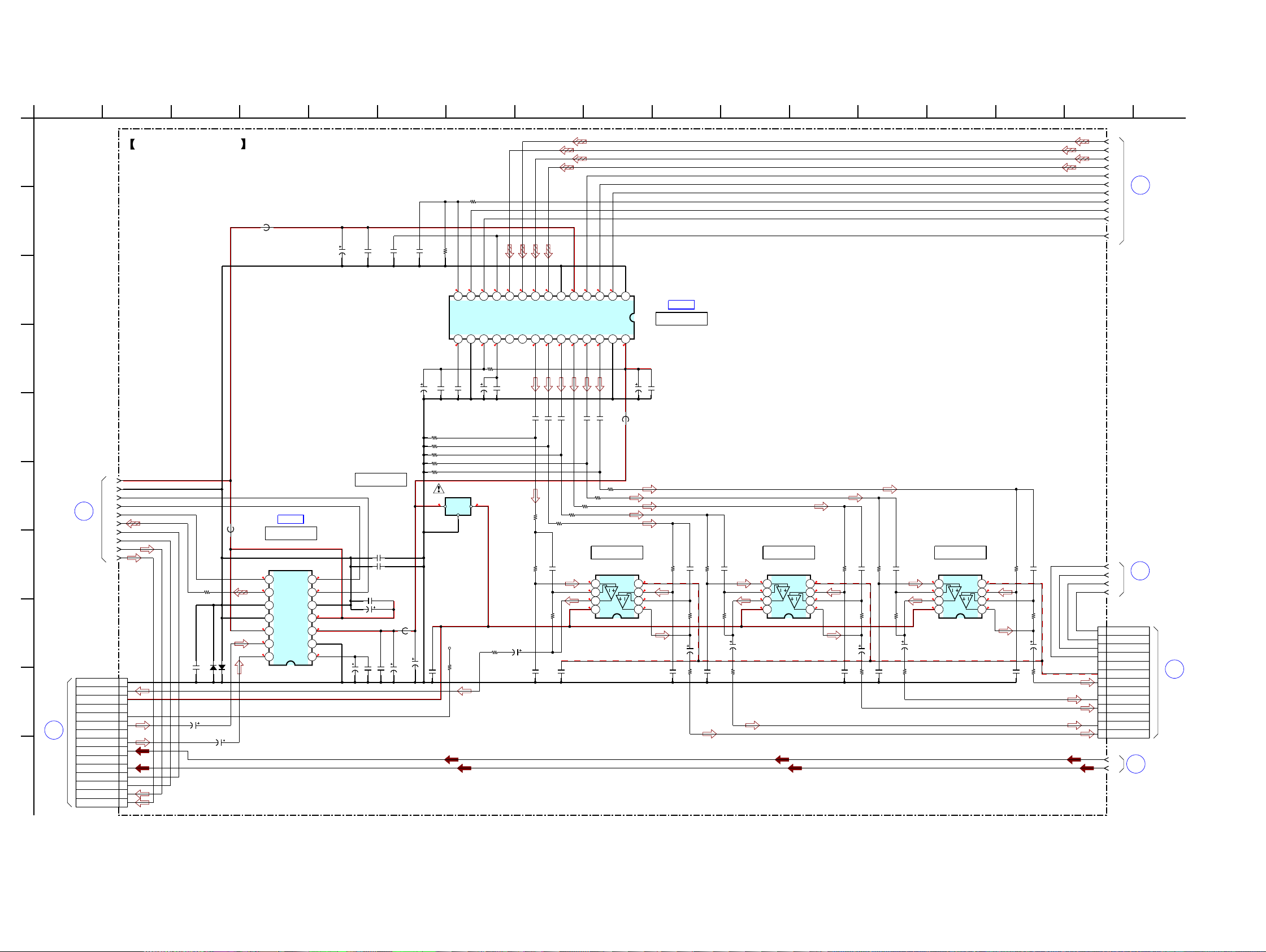
STR-K7200
STR-K7200
2626
• See page 48 for IC Block Diagrams.
6-11. SCHEMATIC DIAGRAM - DIGITAL AB Board (2/5) -
(2/3)
A
MAIN
BOARD
CNP410
(3/5)
AB BOARD
DIGITAL
16
IC B/D
IC B/D
DIGITAL
AB BOARD
17
(5/5)
DIGITAL
AB BOARD
18
(4/5)
(2/3)
B
(1/5)
11
BOARD
MAIN
AB BOARD
DIGITAL
CNP411
-7
0
0
0
0
0
0
7
-7
2.4
2.4
0
0
0
2.4
7
-7
0
0
0
0
0
0
7
1.2
3.3
1.6
2.1
1.6
3.3
1.6
5
2.1 2.1
000.2
3.3
0
1.7
0.8
0
3.3
1.7
1.7
1.7
1.6
5
2.1
2.2
1
2.2
3
2
2.1
5
75
1k
R1416
680p
C1474
50V
10
C1488
100p
C1320
16V
100
C1457
100
R1200
C1471
0.1
1k
R1486
50V10C1653
R1647
10k
0.1
C1401
330p
C1433
0.1
C1459
6.8k
R1473
50V
10
C1458
16V
100
C1460
C1005 0. 1
680p
C1456
6.8kR1498
R1496
8.2k
8.2k
R1424
0
R1455
33R1148
330p
C1473
50V
1
C1660
50V10
C1406
6.8k
R1493
C1419 0.1
1SS367-T3SONYD1003
330p
C1453
R1643
10k
IC NJM4565M(TE2)
IC1406
R1648
10k
6.8kR1494
0
R1435
50V
10
C1418
0.1
C1004
0.1
C1451
330p
C1413
0.1
C1450
10V
470
C1001
6.8k
R1434
0.1
C1454
6.8k
R1454
1k
R1466
6.8k
R1463
0.1
C1423
50V
1
C1659
330p
C1463
16V
100
C1461
0.47
C1002
680p
C1462
0.01
C1362
0
R1464
6.8kR1497
FB1453
1k
R1436
6.8k
R1414
C1420
0.1
6.8kR1495
1k
R1426
680p
C1432
FB1403
680p
C1411
C1915
0.1
FB1405
0
R1425
50V
10
C1468
0.1
C1405
0.1
C1422
1
2
3
4
5
6
7
8
9
10
11
12
13
14
15
15P
CNS501
AGND
SL OUT
+7V
SBR OUT
SBL OUT
L IN
AGND
R IN
TUNER R
AGND
TUNER L
DMPORT L-
DMPORT RDMPORT L+
DMPORT R+
50V
10
C1428
1SS367-T3SONYD1004
1kR1476
FB1452
220p
C1258
50V
10
C1478
0.1
C1455
16V100
C1465
C1470 0.1
IC NJM4565M(TE2)
IC1405
0.1C1654
1
2
3
4
5
6
7
8
9
10
11
12
13
13P
CNS502
VOL IC CLK
VOL IC DATA
VACS CTRL
PROTECTOR
+7V
-7V
FR OUT
AGND
FL OUT
SW
AGND
C OUT
SR OUT
10k
R1474
28272625242322212016 17 18 1915
12345678913 12 11 1014
WM8766GEDS/ R
IC1452
MODE
MCK
BCK
LRCK
DVDD
DGND
DIN1
DIN2
DIN3
DIN4
M/I2S
MC/IWL
MD/DM
MUTE
TEST_REF
VREF_N
VREF_P
VMID
VO4L_NC
VO4R_NC
VO1L
VO1R
VO2L
VO2R
VO3L
VO3R
AGND
AVDD
R1645
10k
50V10
C1402
7
6
5
4
3
2
1
8
9
10
11
12
13
14
PCM1808PWR
IC1401
VREF
AGND
VCC
VDD
DGND
SCKI
LRCKBCK
DOUT
MD0
MD1
FMT
VINL
VINR
R1644
10k
4
3
2
1
5
6
7
8
4
3
2
1
5
6
7
8
4
3
2
1
5
6
7
8
IC NJM4565M(TE2)
IC1404
100
R1401
C1472 0.1
R1456
1k
0
R1427
0
R1485
IO
G
TA7805S
IC1001
13
2
LINE AMP
IC1405
LINE AMP
IC1406
LINE AMP
IC1404
IC1401
A/D CONVERTER
IC1001
+5V REGULATOR
IC1452
D/A CONVERTER
99
103
107
111
102
106
110
101
105
109
100
104
108
136
135
134
133
53
55
58
54
56
52
59
57
51
60
DIGITAL AB BOARD (2/5)
VDD
VEEVEE
VDD
VEE
VDD
D
B
16 1710 11
F
5 153
G
1 12
C
E
H
8967
J
4 13
A
142
I
(Page 25)
(Page
23)
(Page 27)
(Page 29)
(Page 23)
(Page 28)

STR-K7200
STR-K7200
2727
• See page 35 for Waveforms. • See page 48 for IC Block Diagrams. • See page 55 for IC Pin Function Description.
6-12. SCHEMATIC DIAGRAM - DIGITAL AB Board (3/5) -
(4/5)
AB BOARD
DIGITAL
19
AB BOARD
(5/5)
20
DIGITAL
2
IC B/D
IC B/D
(2/5)
AB BOARD
DIGITAL
16
(1/5)
DIGITAL
15
AB BOARD
1.23.3
1.6
1.6
000
0
0.5
3.3
1.2
3.3
1.2
0
3.301.2
3.3
3.3
1.2
1.2
3.3
1.2
1.2
1.2
3.3
3.3
1.2
0
1.3
3.3
3.3
3.3
1.2
1.7
1.7
1.7
1.7
1.2
3.3
1.7
1.2
0
1.2
1.2
1.2
1.2
1.2
1.2
1.2
3.3
1.2
1.2
3.3
1.2
3.3
0
1.2
1.2
1.2
3.3
3.3
3.3
3.3
0
1.2
1.2
3.3
1.2
1.2
3.3
1.2
1.701.2
1.2
0.801.2
1.7
1.6
3.3
1.7
3.3
3.3
1.6
3.3
1.6
1.7
1.6
0
1.3
2.2
1.3
1.7
2.2
1.7
3.3
1.6
2.2
1.7
1.7
2.2
1.7
0.1
C1094
0.1
C1127
10
C1105
16 15 14 13
12 11
10 9
8765
4321
TC74VHC157FT(EL)
IC1008
SA0B0Y0A1B1Y1
GND
Y2
B2
A2
Y3
B3
A3
E
VCC
22
R1038
0R1100
0.1
C1039
10k
R1050
0.1
C1107
10k
R1146
47
R1018
22
R1031
0.1
C1058
0.1
C1116
0.1
C1065
0.1
C1097
0R1101
330
R1556
373839404142434445464748495051525354555657585960616263646566676869707172
73
74
75
76
77
78
79
80
81
82
83
84
85
86
87
88
89
90
91
92
93
94
95
96
97
98
99
100
101
102
103
104
105
106
107
108
36
35
34
33
32
31
30
29
28
27
26
25
24
23
22
21
20
19
18
17
16
15
14
13
12
11
10
9
8
7
6
5
4
3
2
1
109 110 111 112 113 114 115 116 117 118 119 120 121 122 123 124 125 126 127 128 129 130 131 132 133 134 135 136 137 138 139 140 141 142 143 144
ADSST-AVR-1115
IC1009
VDDINT
CLKCFG0
CLKCFG1
BOOTCFG0
BOOTCFG1
GND
VDDEXT
GND
VDDINT
GND
VDDINT
GND
VDDINT
GND
FLAG0
FLAG1
AD7
GND
VDDINT
GND
VDDEXT
GND
VDDINT
AD6
AD5
AD4
VDDINT
GND
AD3
AD2
VDDEXT
GND
AD1
AD0
WR*
VDDINT
VDDINT
GND
RD
ALE
AD15
AD14
AD13
GND
VDDEXT
AD12
VDDINT
GND
AD11
AD10
AD9
AD8
A16 DAI_PI
VDDINT
GND
A17 DAI_P2
A18 DAI_P3
GND
VDDEXT
VDDINT
GND
PF_CE DAI_P4
SPI_MAS DAI_P5
DPSOA DAI_P6(L&R)
DPSOB DAI_P7(SL&SR)
VDDINT
GND
VDDINT
GND
DSPOC DAI_P8(C&SW)
(SBL&SBR)
DSPOD DAI_P9
VDDINT
VDDEXT
GND
VDDINT
GND
DAI_P10 DPSOE
DAI_P11 DPSIA
DAI_P12 DPSIB
DAI_P13 DPSIC
DAI_P14 DPSID
DAI_P15 DPSIE
VDDINT
GND
GND
DAI_P16 DPDVLRCK
DAI_P17 DPDVBCK
DAI_P18 DPLRCK
DAI_P19 DPBCK
VDDINT
GND
GND
VDDEXT
DAI_P20 DPFSCK
GND
VDDINT
FLAG2 NONAUDIO*
FLAG3 SF_CE*
VDDNT
GND
VDDINT
GND
VDDINT
GND
VDDINT
GND
VDDINT
VDDINT
GND
VDDINT
GND
VDDINT
GND
VDDINT
GND
VDDEXT
GND
VDDINT
GND
VDDINT
RESET
SPIDS
GND
VDDINT
SPICLK
MISO
MOSI
GND
VDDINT
VDDEXT
AVDD
AVSS
GND
CLKOUT
EMU
TDO
TDI
TRST
TCK
TMS
GND
CLKIN
XTAL
VDDEXT
0.1
C1077
16V
100
C1063
FB1112
0.1
C1088
0.1
C1098
0
R1080
22R1047
22R1043
22R1068
0.1
C1054
0.1
C1056
10k
R1053
0.1
C1096
10V
220
C1073
0.1
C1059
0.1
C1060
0.1
C1057
470
R1054
0.1
C1093
22
R1040
470
R1049
10k
R1037
0.1
C1041
10k
R1071
0
R1103
50V
10
C1017
10kR1033
100
R1142
FB1104
0.1
C1061
22
R1030
0.1
C1072
FB1105
FB1053
10k
R1069
22R1062
0.1
C1068
0.1
C1051
0.01
C1104
0.1
C1069
0
R1084
0.1
C1083
0.1
C1087
0.01
C1099
16V
100
C1179
0
R1070
22
R1029
D1504
0.1
C1191
1M
R1048
0.1
C1055
8p
C1048
10
C1078
0.1
C1118
100k
R1530
0.1
C1016
0.1
C1119
VCC
GND
OUT
BD12KA5FP-E2
IC1002
1
3
2
0.1
C1117
0.1
C1053
220R1023
0.1
C1085
0R1102
25MHz
X1302
0.1C1113
22
R1028
C1075
0.47
FB1102
7654321
8 9 10 11 12 13 14
TC74VHC393FT(EL)
IC1016
CKA
RDA
Q1A
Q2A
Q3A
Q4A
GNDQ4B
Q3B
Q2B
Q1B
RDB
CKB
VCC
0.1
C1084
D1501
0
R1036
0.1
C1095
0.1
C1115
C1074
0.1
10
C1062
0.1
C1070
0.1
C1028
C1044
8p
0R1104
10
C1092
0.1
C1109
D1503
100R1131
22R1046
1k
R1034
16V
100
C1064
0.1
C1052
FB1503
16V
100
C1076
D1502
8
7
6
5
4
3
2
1
TC7WH74FU(TE12R)
IC1014
CK
D
Q
GND Q
CLR
PR
VCC
0.1
C1110
0.1
C1080
0.1
C1050
FB1106
0.1
C1047
50V10C1102
100R1017
10k
R1035
D FLIP-FLOP
IC1014
BUFFER
IC1016
DATA SELECTOR
IC1008
DSP
IC1009
116
119
120
115
118
124
117
123
114
121
122
125
126
127
131
130
129
128
132
78
82
81
79
80
88
90
87
84
94
83
89
85
93
86
95
92
91
98
105
103
96
104
101
102
100
99
97
109
107
108
106
DIGITAL AB BOARD (3/5)
IC1002
+1.2V REGULATOR
1SS367-T3SONY
1SS367-T3SONY
1SS367-T3SONY
1SS367-T3SONY
D
B
16 1710 11
F
5 15
L
K
3
G
1 1812
C
E
H
8967
J
4 13
A
142
I
(Page
25)
(Page
26)
(Page 28)
(Page 29)

STR-K7200
STR-K7200
2828
• See page 48 for IC Block Diagrams.
6-13. SCHEMATIC DIAGRAM - DIGITAL AB Board (4/5) -
IC B/D
(3/5)
19
DIGITAL
AB BOARD
AB BOARD
DIGITAL
22
(1/5)
CN101
BOARD
XM
P
AB BOARD
(1/5)
13
DIGITAL
AB BOARD
(2/5)
18
DIGITAL
R
CNS271
VIDEO
BOARD
CN350
(3/3)
BOARD
MAIN
F
CN4102
T
CONVERTER
DCDC
BOARD
(3/3)
CN941
L
MAIN
BOARD
BOARD
U
STANDBY
CNP913
(5/5)
DIGITAL
AB BOARD
21
3.37.1
56.3
5
3.8
3.3
3.3
16.19
123
3P
CNP512
DGND
+6.3V
+4.1V
1k
R1260
8.2k
R1468
0.47
C1021
MA2J1110GLS0
D1111
VCC
GND
OUT
BA50BC0FP-E2
IC1031
3
1
2
12345
SI-3033KM-TL
IC1013
E
VIN
GND
VOUT
SENSE
50V
22
C1185
4.7k
R1367
1SR154-400TE-25
D1001
0
R1120
0.1
C1086
25V
47
C1914
MA2J1110GLS0
D1107
C1120
0.1
FB1113
100R1802
1
2
3
4
5
6
7
8
9
9P
CNS508
L_CH
VCC
R_CH
GND
SD
CE
DI
CLK
DO
50V
0.47
C1031
10V
100
C1187
1k
R1261
MA2J1110GLS0
D1108
0.47
C1913
10V
470
C1032
10V
470
C1022
1
2
3
4
5
6
7
7P
CNS503
XMDACMS
XMDACMC
XMDACMD1
XMDBPOWER
XMMOXMI
XMMIXMO
XMRESET
MA2J1110GLS0
D1112
1
3456789
10
10P
CNP505
+15V2NC
R2 GND (NC)
POWER_RY
STANDBY GND
STOP (AC-OFF-DET)
STANDBY (+9V)
SUB-T (CEC)
+7V (R4)
GND (R4)
1
2
3
4
5
6
7
7P
CNS509
V_SW4
V_SW3
V_SW2
V_SW1
COMP_S1
COMP_S2
PS (V-MUTE)
VCC
GND
OUT
BA33BC0T
IC1904
3
1
2
12345
6
6P
CNP504
HP_DETECT
HP RY
C/SUR/SB_RY
FRONT B RY (NC)
SW PREOUT RY
FRONT A RY
IO
G
TA7809S
IC1902
13
2
+3.3V REGULATOR
IC1013
+3.3V REGULATOR
IC1904
+5V REGULATOR
IC1031
+9V REGULATOR
IC1902
64
111
110
137
138
144
142
140
139
141
143
DIGITAL AB BOARD (4/5)
114
149
151
157
167
154
171
161
158
145
168
153
172
160
148
170
156
163
165
146
159
164
147
152
166
162
W1000-W1001
(FM/AM)
TUNER
ANTENNA
AM
COAXIAL
FM 757
D
B
1610 11
F
5 153
G
1 12
C
E
H
89674 13
A
142
(Page 25)
(Page 41)
(Page 26)
(Page 24)
(Page 45) (Page 47)
(Page 24)
(Page 25)
(Page 33)
(Page 27)
(Page 29)

STR-K7200
STR-K7200
2929
CNS110
BOARD
S
DISPLAY
DIGITAL
21
(4/5)
AB BOARD
AB BOARD
DIGITAL
14
(1/5)
AB BOARD
DIGITAL
20
(3/5)
AB BOARD
DIGITAL
12
(1/5)
AB BOARD
DIGITAL
17
(2/5)
3
3.3 3.3
0
3.3
3.3
3.3
3.3
3.3
3.3
3.3
3.3
3.3
0
0
0
3.3
3.3
1.6
3.3
0
3.2
3.3
1.5
1.3
3.3
3.3
3.3
0
0
2.7
3.9
0
0.3
3.3
3.3
3.3
1.9
0
3.3
3.3
3.3
0
3.3
3.3
3.3
3.9
3.3
3.3
3.3
3.3
0
3.3
3.3
3.3
3.3
3.303.2
3.2
0
0
3.3
3.2
3.203.3
0
0
3.303.3
0
0
2.9
0.1
3.3
3.3
3.203.3
3.3
1.5
3.300
3.3
3.4
3.9
0.1
0.1
0.103.3
3.2
3.203.20000
3.203.3
003.3
0
3.3
3.3
0
0
3.2
3.2
3.32.7
2.7
0
3.3
1.6
2.7 2 .7
10kR1179
100
R1155
100
R1126
100R1801
220p
C1132
0
R1157
100
R1042
100
R1138
10kR1635
10kR1187
100p
C1067
1k
R1175
FB1308
10k
R1192
0.1C1667
100
R1021
47k
R1949
0.1
C1126
100R1199
3.3k
R1072
100
R1014
3.3k
R1159
10kR1180
10kR1636
8
7
6
54
3
2
1
S-24CS16A0I-J8T1G
IC1131
A0
A1
A2
GND SDA
SCL
WCB
VCC
100
R1807
10k
R1039
100R1135
220p
C1131
0
R1156
100R1129
22
R1144
0.1C1121
100R1134
100
R1804
100R1124
10kR1191
100
R1013
0.1C1604
100
R1168
0.1C1620
100R1012
0.01
C1129
10kR1181
0
R1964
100
R1106
100R1806
100p
C1168
100R1326
0.01C1171
100
R1201
R1196
100
2.2k
R1109
0.1
C1079
0.1C1100
0.1
C1123
2.2k
R1111
0.1
C1139
25V47
C1103
100
R1127
10kR1182
0.1C1605
FB1101
1k
R1117
100
R1125
47k
R1164
100
R1202
100
R1197
10k
R1105
10k
R1097
1k
R1132
100
R1123
100
R1122
10k
R1203
100R1076
10kR1088
100
R1115
0.01C1172
10kR1186
0.1
C1140
100
R1174
100
R1158
10kR1083
100R1078
2.2k
R1107
3.3k
R1073
C1066
100p
0.1
C1122
100R1077
31
32
33
34
35
36
37
38
39
40
41
42
43
44
45
46
47
48
49
50
51
52
53
54
55
56
57
58
59
60
61 62 63 64 65 66 67 68 69 70 71 72 73 74 75 76 77 78 79 80 81 82
83 84 85 86 87 88 89 90
30 29 28 27 26 25 24 23
22 21 20 19 18 17 16 15 14 13 12 11 10 9
87654321
91
92
93
94
95
96
97
98
99
100
101
102
103
104
105
106
107
108
109
110
111
112
113
114
115
116
117
118
119
120
MB91353APMT-G-117E1
IC1010
DAC CLK
/XMDACMC
XMDACMS
XMDACMD1
DAC_DI
TUNING A
TUNING B
HDMI_REG_CTRL
DSP_SELECT
POWER_RY
VOL_CL
VOL_DA
HP_DETECT
HP_RY
C/SUR/SB
FRONT B/ST SW RY
SW RY
FRONT A RY
VSS
VCC
SBR RY
TUNE_LAT
TUNE_DI
T_CLK
TUNE_DO
FUSE_DETECT
DAC_ATC
DAC_MUTE
CEC_OUT
DIR_XSTATE
HDMI_ERR
V_SW4
V_SW3
V_SW2
V_SW1
COMP_S1
COMP_S2
PS(V-MUTE)
DIR_XMODE(RESET)
DIRCKST
VSS
NO USE
NO USE
VSS
VCC
DIR_CLK
DIR_CE(LAT)
DIR_DI
DIR_DO
DIR_ERROR
HDMI_FSRATE
NMI
MD2
MD1
MD0
INIT
VCC
X1
X0
VSS
X0A
X1A
RESET_TRG
DIR_DATAO
DSP RESET
DSP SPDIDS(LAT)
74ACT153_B
74ACT153_A
PROTECTOR
FL LAT
FL_CLK
FL_DATA
NO USE
DSP MISO
DSP MOSI
DSP SPICLK
VSS
VCC
EEPROM CLK
VOL_JOG(2B)
VOL_JOG(2A)
DSPINT
DCAC_DSP_IN
STOP
SIRCS_IN
POWER KEY
RDS INT/XMDBPOWER
RDS DATA
CEC IN
INPUT ENCODER A
INPUT ENCODER B
NO USE
XMIXM0
XMMOXI
XMRESET
VCC
VSS
SUBT
EEPROM DATA
CLINK_TX
CLINK_RX
CLINK_DET
FLASH2/HDMI_UART_RX
FLASH1/HDMI_UART_TX
HDMI RESET
NO USE
NO USE
DAVS(GND)
DAVC(3.3V)
AVCC(3.3V)
AVRH(3.3V)
AVSS/AVRL(GND)
VSS(GND)
AD KEY1
AD_KEY2
DCAC_IN
VERSION
RDS SIGNAL
MODEL
VACS_CTRL
NO USE
0
R1151
0.1
C1125
100R1140
100R1313
RB751V-40TE-17
D1106
0.1C1108
100R1128
RT1N141C-TP-1
Q1103
10k
R1119
220
R1512
4700p
C1704
50V
1
C1081
4
3
2
1
TC7W14FU(TE12R)
IC1005
100k
R1011
2SC4154TP-1EF
Q1104
0.1C1101
ISA1602AM1TP-1EF
Q1106
10k
R1515
0
R1509
27k
R1511
3
2
1
5
6
7
8
4
5
TC7S08FU(TE85R)
IC1006
1k
R1447
22k
R1514
22k
R1513
0.1
C1082
0.1
C1701
2SC4154TP-1EF
Q1105
10k
R1510
100p
C1112
10kR1116
0
R1508
10kR1044
0.1
C1142
0.1
C1124
100
R1160
1
2
3
4
5
6
7
8
9
10
11
12
13
14
15
16
17
17P
CNS510
DCAC_IN
INPUT_JOG B
INPUT_JOG A
FL CLK
FL DATA
FL LAT
AD1
AD2
SIRCS
PW_SW
VOL JOG 2B
VOL JOG 2A
+5V
+3.3V
5V GND
3.3V GND
NC
2.2k
R1136
100
R1066
100
R1067
100R1010
100
R1015
100
R1016
100R1022
100
R1025
100
R1118
100
R1137
0.01C1254
0.01C1255
10k
R1161
10kR1253
100
R1162
FB1311
0.1
C1049
100R1327
100
R1112
0.01
C1612
0.01
C1613
0.01C1614
0.01C1615
0.01C1616
0.01C1617
0.01C1618
0.01C1619
0.01
C1621
0.01
C1650
0.01
C1622
0.01C1623
0.01C1624
0.01C1629
0.01C1630
0.01C1628
0.01C1627
0.01C1626
0.01C1625
0.01C1631
0.01C1634
0.01C1632
0.01C1633
0.1C1652
3
2
1
4
5
IC1007
S-80929CNMC-G8ZT2G
SYSTEM CONTROLLER
IC1010
RESET SWITCH
IC1006
RESET SIGNAL
IC1007
EEPROM
IC1131
61
62
63
74
67
66
68
65
69
75
73
76
71
70
72
121
118
115
120
119
117
116
123
122
124
129
131
127
126
132
130
128
125
133
134
140
138
137
141
139
142
144
143
145
151
149
147
146
148
156
158
157
152
153
154
159
160
161
162
164
163
165
167
166
170
168
172
171
DIGITAL AB BOARD (5/5)
77
135
136
12.5MHz
X1101
NCCDVSS
OUT
VDD
GND
VCC
GENERATOR
RESET SIGNAL
BUFFER
IC1005
Q1103-1106
CEC DATA SWITCH
GND
VCC
D
B
16 1710 11
F
5
N
15
L
K
193
G
1 1812
C
M
E
H
8967
J
4 13
A
142
I
R1194
0
R1163
22k
Note: IC1131 cannot exchange with single. When IC1131
is damaged, exchange the entire mounted board.
• See page 35 for Waveforms. • See page 55 for IC Pin Function Description.
6-14. SCHEMATIC DIAGRAM - DIGITAL AB Board (5/5) -
(Page 25)
(Page
27)
(Page 25)
(Page 26)
(Page 43)
(Page 24)

STR-K7200
STR-K7200
3030
Note: IC1131 cannot exchange with single. When IC1131
is damaged, exchange the entire mounted board.
6-15. PRINTED WIRING BOARD - DIGITAL AB Board (Component Side) -
• : Uses unleaded solder.
• See page 20 for Circuit Boards Location.
BE
BE
B
E
B
E
8
9
16
144
1
108
109
73
72
36
37
1
120
30
31
61
60
90
91
15
1
1
14
87
114
15
28
2176
1
18
1
2
17
16
2
17
6
5
8
14
C1118
C1119
C1310
C1312
C1313
C1314
C1315
C1122
C1316
C1317
C1123
C1701
C1127
C1704
C1129
D1106
D1107
C1320
D1108
R1105
R1106
R1107
C1131
R1109
D1301
C1132
D1111
R1301
D1112
R1302
FB1403
R1303
R1304
C1139
R1111
C1909
FB1405
R1305
R1112
R1306
R1307
R1308
R1115
IC1301
R1116
IC1302
R1117
IC1303
R1118
R1119
C1142
R1310
C1915
R1311
R1313
R1120
R1508
R1509
R1122
R1123
R1124
R1318
R1125
R1319
R1126
R1127
R1128
R1510
R1129
R1511
R1512
R1513
R1514
R1321
R1515
R1323
R1130
R1324
R1131
R1325
R1132
R1326
R1327
R1133
R1134
R1135
R1136
R1137
R1138
R1139
IC1131
C1358
R1140
R1141
R1142
R1144
C1361
C1362
R1146
FB1053
R1147
R1148
R1151
R1155
R1156
R1157
R1158
R1159
R1351
FB1453
R1160
R1354
R1161
R1162
R1356
R1357
R1358
R1359
R1168
C1191
R1360
R1362
R1556
R1940
R1366
R1367
R1174
R1368
R1175
R1949
R1186
R1187
R1191
R1192
R1964
R1196
R1197
R1199
X1101
C1010
C1011
C1012
C1016
J1302
C1401
X1301
X1302
C1405
CNS503
D1001
C1028
C1604
CNS509
C1411
C1605
FB1101
FB1102
C1413
FB1103
C1419
CNS512
R1200
IC1005
R1201
C1612
IC1006
R1202
C1613
IC1007
R1203
C1614
C1420
R1010
IC1008
C1615
C1039
R1011
IC1009
FB1305
C1616
FB1306
C1422
FB1112
R1012
C1617
FB1307
C1423
FB1113
R1013
C1618
R1014
FB1308
C1619
R1015
FB1309
R1016
FB1117
R1017
R1018
IC1010
C1041
R1401
IC1013
FB1503
C1044
C1620
IC1014
C1622
IC1016
C1623
C1047
IC1017
C1624
C1048
C1625
R1021
IC1401
C1626
R1022
C1432
C1627
C1433
R1023
C1628
IC1404
C1629
R1025
IC1405
IC1406
851
4
C1050
R1028
C1051
R1029
C1052
C1053
C1630
C1054
R1414
C1631
C1055
C1632
C1056
R1416
C1633
C1057
C1634
C1058
R1030
C1059
R1031
R1801
R1802
R1034
R1804
R1036
R1806
R1807
C1060
R1038
C1061
C1258
R1424
C1065
R1425
R1426
R1427
C1068
C1450
R1040
C1069
C1451
R1041
R1042
C1453
R1043
C1454
R1044
C1455
C1456
R1046
R1047
C1070
R1048
C1459
R1049
C1072
C1650
C1074
R1434
R1435
R1436
C1077
C1654
R1050
C1079
C1462
C1463
R1053
R1054
C1080
R1635
C1082
R1636
C1083
C1084
FB1350
C1085
C1086
C1087
R1253
R1447
C1088
C1470
C1089
C1471
C1472
R1062
C1473
C1667
R1063
C1474
R1066
R1067
R1068
R1069
C1093
C1094
R1454
C1095
R1455
C1096
R1456
C1097
C1098
R1070
C1099
R1071
IC1452
R1076
R1077
R1078
R1463
R1464
R1466
R1080
R1468
JR1005
R1083
R1084
R1473
R1474
R1476
R1485
R1486
R1493
R1494
R1495
R1496
R1497
R1498
LP1000
C1101
C1104
C1107
Q1103
C1108
Q1104
C1109
Q1105
Q1106
C1301
C1302
C1303
C1110
C1304
C1305
C1112
C1113
C1114
C1115
C1309
C1116
C1117
851
4
851
4
1481
7
16
918
8
5
1
4
8
5
1
4
8
5
1
1
12
36
25
2413
3748
4
DIGITAL AB BOARD (COMPONENT SIDE )
1-875-597-
11
(11)
P
XM BOARD
CN101
V
HDMI BOARD
CN3511
R
VIDEO BOARD
CNS271
4
3
1
5
4
3
1
5
415
8
DMPORT
A
B
C
D
E
F
G
12345678 9
Ref. No. Location
• Semiconductor
Location
D1001 C-9
D1106 G-8
D1107 B-6
D1108 B-6
D1111 B-6
D1112 B-6
D1301 D-3
IC1005 G-8
IC1006 G-8
IC1007 G-9
IC1008 E-3
IC1009 D-5
IC1010 E-8
IC1013 C-7
IC1014 E-4
IC1016 E-4
IC1017 C-4
IC1131 F-9
IC1301 C-3
IC1302 C-2
IC1303 D-2
IC1401 G-2
IC1404 G-5
IC1405 G-6
IC1406 G-7
IC1452 F-4
Q1103 G-8
Q1104 G-8
Q1105 F-8
Q1106 F-8
(Page 40) (Page 36)
(Page 32)

STR-K7200
STR-K7200
3131
6-16. PRINTED WIRING BOARD - DIGITAL AB Board (Conductor Side) -
• : Uses unleaded solder.
• See page 20 for Circuit Boards Location.
C1318
C1923
C1355
C1359
C1370
C1001
C1006
C1008
C1009
C1017
C1402
C1406
C1063
C1457
C1653
C1460
C1461
C1465
C1659
C1660
C1102
C1306
C1307
C1914
C1179
C1185
C1187
C1022
C1418
C1032
W1000
C1428
C1064
C1458
C1073
C1076
C1468
C1081
C1478C1488
C1103
8
9
1
2
1
6
CNS508
CNP504
1
3
HS1904
IC1904
10
1
3
8
9
CNP505
1
2
16
17
CNS510
1
3
I
CN1008
IC1001
115
1
13
CNS501
CNS502
IC1351
IC1352
1
3
1
3
IC1902
CNP512
1
5
C1120
C1121
C1124
C1319
C1125
C1126
R1100
R1101 R1102
R1103
R1104
C1907
D1501
D1502
D1503
C1140
D1504
C1913
R1314
C1351
C1354
C1168
R1530
C1171
C1172
R1350
FB1452
R1352
R1353
R1355
J1301
R1163
R1164
R1179
R1180
R1181
R1182
R1194
C1002
C1004
C1005
C1007
C1021
D1003
D1004
FB1104
FB1105
FB1106
C1031
IC1002
FB1302
R1019
IC1012
FB1310
C1621
FB1311
C1049
R1033
R1035
R1037
C1254
C1255
R1039
IC1031
C1062
C1066
C1067
C1075
C1652
C1078
R1643
R1644
R1645
C1092
R1647
R1260
R1648
R1261
R1072
R1073
JR1003
R1088
R1097
C1100
C1105
W1001
1-875-597-
11
(11)
(CONDUCTOR SIDE)
DIGITAL AB BOARD
3
2
1
1
2
3
F
MAIN BOARD
CN350
U
STANDBY
BOARD
CNP913
L
MAIN
BOARD
CN941
S
DISPLAY
BOARD
CNS110
Q
VIDEO BOARD
CNP242
3
1
A
MAIN BOARD
CNP410
B
MAIN BOARD
CNP411
3
1
3
1
T
DCDC CONVERTER
BOARD
CN4102
TUNER
(FM/AM)
FM 75Ω
COAXIAL
ANTENNA
DIGITAL
AM
TV
OPTICAL
IN
OPTICAL
SAT IN
COAXIAL
DVD IN
A
B
C
D
E
F
G
H
123456789 10
Ref. No. Location
• Semiconductor
Location
D1003 F-7
D1004 F-7
D1501 D-7
D1502 D-7
D1503 D-7
D1504 E-7
IC1001 G-7
IC1002 C-5
IC1012 E-9
IC1031 B-3
IC1351 D-9
IC1352 B-9
IC1902 B-4
IC1904 B-2
(Page 44)
(Page 21)
(Page 46)
(Page 21)
(Page 42)
(Page 21)
(Page 21)
(Page 40)

STR-K7200
STR-K7200
3232
6-17. PRINTED WIRING BOARD - XM Board -
• : Uses unleaded solder.
• See page 20 for Circuit Boards Location.
1
8
9
16
1
3
2
1
7
6
1
5
EP101
EP102
Q105
Q106
L101
L102
FB101
FB104
R101
R102
R103
R104
R107
R108
R109
R110
R112
R115
R116
R117
R118
R119
CN101
CN102
R120
R121
R123
R124
R126
R127
R128
R130
R131
R132
R133
R137
R138
C101
C102
C103
C104
R143
R144
C108
R145
R146
R147
C110
C111
X101
12
1
13
48
36
37
24
25
C113
C118
C119
R156
R158
C120
C121
C122
C123
C124
C125
R162
C126
R163
C127
C128
C129
C130
C131
C132
C133
C134
C135
C136
C137
C138
R174
C139
R176
C140
C142
C143
C144
C145
C153
C157
C159
D101
C161
C163
D103
C164
C165
C166
C174
C175
C176
IC101
IC102
IC104
IC105
IC106
IC107
CNP103
J101
E
E
C105
C106
C107
C109
R122
R125
C116
R129
R134
1
45
8
XM BOARD
(COMPONENT SIDE)
XM BOARD (CONDUCTOR SIDE)
(CHASSIS)
(CHASSIS)
1
4
A
K
XM
K
D
MAIN
BOARD
CN434
P
DIGITAL
AB BOARD
CNS503
W
DCDC
CONVERTER
BOARD
CN4102
1-875-744-
11
(11)
1-875-744-
11
(11)
1
4
5
2
3
1
3
2
3
1
2
+
+
+
+
+
+
+
+
+
+
+
A
B
C
12345 6
Ref. No. Location
• Semiconductor
Location
D101 B-2
D103 B-1
IC101 C-3
IC102 B-2
IC104 B-3
IC105 B-3
IC106 C-2
IC107 C-3
Q105 C-2
Q106 C-2
(Page 30)
(Page 21)
(Page 44)

STR-K7200
STR-K7200
3333
• See page 35 for Waveforms. • See page 48 for IC Block Diagrams. • See page 55 for IC Pin Function Description.
6-18. SCHEMATIC DIAGRAM - XM Board -
DIGITAL
P
AB BOARD
CNS503
(4/5)
BOARD
(2/3)
D
CN434
MAIN
IC B/D
IC B/D
11
12
13
14
BOARD
CONVERTER
DCDC
CN4102
W
0
3.2
3.3
3.3
0
3.3
3.3
3.3
3.3
0
0
3.3
3.3
1.2
1.2
3.3
1.2
1.2
3.3
0
3.3
0
1.7
1.7
3.3
1.7
0
1.6
3.3
1.6
0
3.3
0
3.3
3.3 5
1.71.7
0
1.7
5
2.5
2.5
3.3
0
2.5
0
56.3
1.3
5.3
6.3
6.3
5.3 5.3
3.2
0.1
5.3
7
0
0
0
0
-6.9
47kR122
47kR145
FB101
4P
J101
1
2
3
4
16
15
14
13
12
11
10
98
7
6
5
4
3
2
1
PCM1753DBQR
IC105
100kR102
0
L102
47kR118
100R108
10kR115
47kR146
100R107
10kR147
10k
R103
4.7k
R158
100k
R101
FB104
47kR121
100k
R128
VCC
GND
OUT
BA33BC0FP-E2
IC101
1
3
2
4321
5678
NJM4565M(TE2)
IC104
10kR116
100
R130
220R125
45.1584MHz
X101
12k
R120
680
R123
1kR138
100
R131
10k
R104
680
R133
10k
R112
100R127
0.47
C161
KDS160-RTK
D103
VCC
GND
OUT
BA50BC0FP-E2
IC107
13
2
680
R174
12k
R137
100
R110
0.47
C157
0.47
C102
150R156
47kR109
100R129
0
L101
8.2k
R124
NSAD500F-T1B
D101
100
R143
100kR126
1kR144
8.2k
R132
100
R134
DTC114YKA-T146
Q105
10k
R176
47kR119
100
R117
12345
BA00BC0WFP-E2
IC106
16V
100
C101
16V
100
C159
50V10
C104
50V
10
C122
50V
10
C125
16V
100
C145
16V100C153
50V
10
C137
50V
10
C113
50V
10
C142
50V
10
C139
0.1
C103
0.1
C108
0.1
C105
0.1
C110
0.1
C123
0.1
C121
0.1
C111
0.1
C116
0.1
C124
0.1
C138
0.1
C140
0.1
C127
0.1
C126
0.1
C136
0.1
C130
0.1
C119
0.1
C144
0.1
C143
1000p
C107
1000p
C109
1000p
C106
5p
C166
5p
C165
22pC131
22pC132
22pC134
22pC133
100p
C174
100p
C176
100p
C175
680p
C118
680p
C129
6800pC120
6800p
C128
0.01
C135
0.1
C164
0.1
C163
1
2
3
3P
CNP103
13
14
15
16
17
18
19
20
21
22
23
24
25 26 27 28
29 30 31 32 33 34 35 36
12 11 10 9
87654321
37
38
39
40
41
42
43
44
45
46
47
48
F2602E-01-TR
IC102
LSOPTXRX
VSS
SCTXOUT
VDD
SRCXIN
VSS
COMMSEL
VDD
IRQ*
VSS
RESET*
SLAVESL
COMRXDIG
COMTXDIG
COMTXEN
VSS
VDD
COMRXP
COMRXM
VDD
VSS
COMTXM
COMTXP
VSS
VSS
OSCOUT
VDD
OSCIN
VSS
TEST
VSS
HSDPDATA
VDD
HSDPCLK
VSS
HSDPEN
I2SDATA
VSS
I2SSCLK
VDD
I2SLRCLK
VSS
I2SOCLK
VSS
SAIICLK
VDD
SAIIDATA
SAIIEN
2SB1689-T106
Q106
1
2
3
4
5
6
7
7P
CN101
100k
R162
330k
R163
1
2
3
4
5
5P
CN102
VCOM
XMDACMS
ZEROL
MC
DGND
VOUTR
AGND
XMMOXMI
VOUTL
BCK
DATA*
6.3VDC
ML(MS)
LRCK
XMRESET
DGND
XMDACMC
VCC(5V)
ZEROR
DGND
XMDBPOWER
XMDACMDI
MD(MDI )
XMMIXMO
NC
SCK
XMR
XMGND
XML
-7V
+7V
+5V REGULATOR
IC107
+5.5V REGULATOR
IC106
IC104
LINE AMP
IC105
D/A CONVERTER
IC102
XM RADIO RECEIVER
IC101
+3.3V REGULATOR
XM BOARD
EP101
(CHASSIS)
(CHASSIS)
EP102
VCC
VEE
NC
OUT
GND
VCC
CTL
B+ SWITCH
Q105, 106
XM
D
B
10 11
F
53
G
1 12
C
E
89674 13
A
142
(Page 28)
(Page 23)
(Page 45)

STR-K7200
STR-K7200
3434
6-19. PRINTED WIRING BOARDS - MIC/HEADPHONE Section -
• : Uses unleaded solder.
• See page 20 for Circuit Boards Location.
1534
J2000
JW2000
B2000
CN2000
C2002
C2006
C2013
C2014
C2001
C2003
C2005
C2008
C2010
C2011
C2205
TP2000
C2012
C2018
R2000
R2001
R2003
R2005
R2006
R2007
R2008
IC2000
D2013
D2014
R2010
R2015
R2016
R2017
R2018
R2019
1
4
CNP790
J790
BT700
JW700
JW701
C790
C791
TP790
C792
C793
1-875-710-
11
(11)
DCAC BOARD
H
MAIN
BOARD
CNP500
Y
DISPLAY
BOARD
CNP106
(CHASSIS)
1
8
4
5
AUTO CAL MIC
E
MAIN BOARD
CN792
1-875-699-
11
(11)
HEADPHONE BOARD
(CHASSIS)
PHONES
A
B
C
D
123456 7
(Page 21)
(Page 42)
(Page 21)

STR-K7200
STR-K7200
3535
• Waveforms
– DIGITAL AB Board –
– XM Board – – HDMI Board –
– DISPLAY Board –
6-20. SCHEMATIC DIAGRAM - MIC/HEADPHONE Section -
Y
H
BOARD
MAIN
CNP500
(3/3)
BOARD
DISPLAY
CNP106
CN792
BOARD
(3/3)
MAIN
E
7
0
0
0
0
0
0
-6.9
50V
1
C2013
50V
1
C2002
50V
1
C2006
50V
0.47
C2014
1.2k
R2018
1k
R2000
1k
R2006
10k
R2001
10k
R2003
10k
R2010
33k
R2015
15k
R2016
10k
R2007
560k
R2008
1M
R2005
100p
C2001
33p
C2005
56p
C2008
2.2k
R2017
2.2k
R2019
1
3
4
5
5P
CN2000
+7V
2
NC
GND
-7V
DCAC_IN
0.022
C2011
0.022
C2012
0.1
C2018
0.033
C2003
0.033
C2010
MA2J1110GLS0
D2013
MA2J1110GLS0
D2014
J2000
C2205
0.1
8765
4321
NJM4565M(TE2)
IC2000
IC2000
MIC AMP
DCAC BOARD
(CHASSIS)
TP2000
AUTO CAL MIC
VCC
VEE
J790
1
2
3
4
4P
CNP790
HP_DETECT
R-CH
GND
L-CH
C791
0.1
HEADPHONE BOARD
TP790
(CHASSIS)
PHONES
D
B
F
531
C
E
674
A
2
(Page 24)
(Page 43)
(Page 24)
IC1301 XB (XOUT)
82 ns
2 V/DIV, 50 ns/DIV
IC1009 [WD (XTAL)
40 ns
500 mV/DIV, 20 ns/DIV
IC1010 UK (X1)
4.3 Vp-p
1.2 Vp-p
IC102 XI (OSCOUT)
RB
22.8 ns
2 V/DIV, 10 ns/DIV
IC102 FM (I2SSCLK)
RT
356 ns
2 V/DIV, 200 ns/DIV
IC102 SB (I2SLRCLK)
RE
4.1 Vp-p
4.6 Vp-p
IC3511 JG (XTALOUT)
XB
35.3 ns
1 V/DIV, 50 ns/DIV
IC3519 RB (XOUT)
XT
100 ns
1 V/DIV, 50 ns/DIV
2.2 Vp-p
3.4 Vp-p
IC100 (OSC)
80 ns
3.9 Vp-p
2 V/DIV, 50 ns/DIV
RG
22.8 μs
2 V/DIV, 10 μs/DIV
IC102 SE (I2SOCLK)
88.5 ns
2 V/DIV, 50 ns/DIV
4.2 Vp-p
4.2 Vp-p
FB
2.2 Vp-p
2.6 μs
1 V/DIV, 2 μs/DIV

STR-K7200
STR-K7200
3636
Note: IC3511 and IC3513 cannot exchange with single.
When IC3511 and IC3513 are damaged, exchange
the entire mounted board.
6-21. PRINTED WIRING BOARD - HDMI Board (Side A) -
• : Uses unleaded solder.
• See page 20 for Circuit Boards Location.
1
A
B
C
D
E
F
G
H
I
2345678910
DCDC
CONVERTER
BOARD
CN4101
X
DIGITAL AB
BOARD
CNS512
V
(CHASSIS)
R3663
CN3503CN3504
OUT
BD IN
DVD IN
SAT IN
CN3510
Q3504
C3548
C3570
C3571
C3572
C3573
R3585
R3779
R3586
R3587
R3588
R3589
R3780
R3590
R3591
R3592
R3599
R3799
FB3501
R3600
FB3513
S1
G1
D2
D1
G2
S2
FB3514
R3634
JL3563
JL3565
JL3566
C3576
C3579
C3580
C3584
C3585
C3586
C3590
C3594
R3784
JL3604
JL3606
JL3614
C3621
FB3506
R3613
R3624
R3625
R3633
JL3593
JL3594
JL3595
JL3596
JL3597
C3591
C3593
R3593
JL3605
JL3609
JL3610
JL3612
JL3613
JL3615
JL3616
JL3618
JL3620
JL3622
C3625
1
5
R3612
R3615
R3622
ET3503
R3660
CN3509
CN3511
D3501
D3502
JL3588
JL3589
JL3590
JL3591
JL3592
R3570
R3798
JL3607
JL3608
JL3611
JL3617
JL3619
JL3621
JL3623
X3502
R3608
C3634
C3635
R3611
JL3506
JL3507
JL3508
C3501
Q3505
C3509
Q3506
C3530
D3511
C3535
C3544
R3711
R3712
R3713
C3547
R3714
R3535
R3536
R3544
R3545
R3750
R3564
R3565
R3566
R3567
C3596
RB3501
RB3502
RB3503
RB3504
RB3505
RB3506
FB3503
FB3509
C3627
1
19 191
R3661
R3662
CN3501CN3502
R3509
D3512
R3511
R3512
R3513
R3744
R3745
C3519
R3514
R3548
R3552
R3556
FB3502
FB3508
FB3512
C3633
R3550
R3554
C3644
R3549
R3551
FB3510
FB3511
C3538
C3540
R3546
C3575
R3741
R3563
X3501
FB3505
C3574
FB3504
R3614
C3643
R3621
R3623
1
1
1
54
132
31
2
5
1
1
2041
60
8061
2140
41
601
20
4021
64 33
32
814916
81
71
1
1
25
75
51
2650
10076
65
96
97 128
6180
5
7
19
1
19
HDMI
1
2
17
16
HDMI BOARD
(SIDE A)
1-872-722-
(11)
11
IC3516
IC3527
IC3528
IC3526
IC3519
IC3511
IC3504
IC3501
IC3503
IC3513
E
E
(NC)
Ref. No. Location
D3501 G-3
D3502 G-3
D3511 E-3
D3512 E-2
IC3501
E-3
IC3503 C-4
IC3504 F-3
IC3511 E-4
IC3513 C-8
IC3516 H-9
IC3519 H-4
IC3526 G-6
IC3527 H-8
IC3528 G-8
Q3504 B-7
Q3505 E-2
Q3506 E-2
• Semiconductor
Location
(Page 44)
(Page 30)

STR-K7200
STR-K7200
3737
6-22. PRINTED WIRING BOARD - HDMI Board (Side B) -
• : Uses unleaded solder.
• See page 20 for Circuit Boards Location.
1
A
B
C
D
E
F
G
H
I
2345678910
R3639
C3502
C3503
C3504
C3505
C3510
C3512
C3514
C3516
C3518
C3521
C3522
C3525
C3526
C3527
R3502
R3504
R3527
R3532
R3534
R3747
R3748
R3749
C3597
R3776
R3655
C3507
C3511
C3513
C3517
C3520
R3526
R3533
R3775
R3654
C3508
R3500
C3531
C3534
C3541
C3542
C3543
C3545
R3716
R3525
R3528
C3553
R3557
R3558
R3595
R3642
Q3507
C3523
C3524
D3513
C3537
C3539
R3519
C3549
R3524
C3550
C3551
C3552
R3541
R3542
R3594
C3533
C3536
R3715
R3521
C3529
R3562
R3610
R3616
R3645
R3652
R3653
R3790
R3791
R3793
C3615
C3616
C3618
R3602
R3603
R3604
R3605
R3700
C3617
C3619
C3620
R3609
R3796
R3797
R3601
R3676
R3506
C3555
C3556
C3557
C3562
C3566
C3568
C3569
R3578
R3579
R3580
R3581
R3582
R3583
R3788
R3597
R3598
C3630
C3631
C3632
C3563
C3564
C3567
R3577
R3584
C3558
C3561
R3576
1-872-722-
(11)
11
HDMI BOARD
(SIDE B)
58
4
1
41
58
8
16 9
1
IC3509
IC3521
IC3507
E
Ref. No. Location
D3513 E-3
IC3507 B-2
IC3509 C-2
IC3521 C-2
Q3507 E-3
• Semiconductor
Location

STR-K7200
STR-K7200
3838
Note: IC3511 cannot exchange with single. When IC3511
is damaged, exchange the entire mounted board.
• See page 35 for Waveforms. • See page 48 for IC Block Diagrams. • See page 55 for IC Pin Function Description.
6-23. SCHEMATIC DIAGRAM - HDMI Board (1/2) -
21
31
HDMI
BOARD
(2/2)
IC B/D
IC B/D
IC B/D
1.8
3.3
3.1
3.3
3.3
3.3
3.3
1.3
3.3
3.3
3.3
3.3
3.3
1.8
3.3
0
3.3
3.3
3.3
3.3
3.3
0
0
0
0
3.3
3.3
3.3
3.3
3.3
3.3
3.3
3.3
3.3
3.3
3.3
0
3.3
2.102.1
3.3
3.3
3.3
3.3
3.3
3.3
3.3
3.3
3.3
3.3
0
3.3
3.1
3
3.2
3.3
2.9
3.3
2.9
3.3
3.3
2.9
3.3
3.3
0
0
0
1.3
1.8
3.3
3.3
0
1.8
3.3
3.3
3
3.2
3.3
2.9
3.3
3.3
2.9
3.3
3.3
2.9
3.3
3.3
1.8
3.3
1.8
3.3
0
0
1.8
3.3
0
0
0
0
0
0
0
0
0
0
0
0
0
0
0
0
0
0
0
0
0
3.3
3.3
1.8
1.8
3.3
0
1.5
1.8
1.8
3.3
3.3
3.3
3.3
3.3
3.3
3.3
3
000
0
0
00000
3.3
3.3
0
3.3
1.2
0
0
3.3
3.3
3.3
3.3
3.3
3.3
3.3
3.3
3.3
3.3
FB3503
47R3565
FB3502
0.1
C3553
0.1
C3552
0.1
C3551
0.1
C3550
0.1
C3549
0.1
C3544
0.1
C3539
0.1
C3535
0.1
C3533
0.1
C3530
0.1C3523
0.1C3524
0.1C3525
0.1C3526
0.1C3527
0.1C3521
0.1C3522
0.1
C3529
0.1
C3531
0.1
C3534
0.1
C3536
0.1
C3537
0.1C3541
0.1C3542
4V220
C3548
100R3549
100R3550
100R3551
100R3552
100R3554
100R3556
47
R3557
0
R3558
0.1
C3545
R3563
100
0R3562
47R3544
47R3545
MAJ21110GLS0
D3501
FB3501
0.5%750
R3525
0.5%
3.9k
R3526
10k
R3527
10k
R3528
0.1
C3516
0
R3502
0
R3504
0
R3506
0R3542
0.1
C3514
0.1
C3520
0R3535
0R3536
8765
4321
BR24L02F-WSE2
IC3509
0.1
C3543
10kR3541
10k
R3534
10k
R3533
10k
R3532
1234567891011121314151617181920212223242526272829303132
33
34
35
36
37
38
39
40
41
42
43
44
45
46
47
48
49
50
51
52
53
54
55
56
57
58
59
60
61
62
63
64
6566676869707172737475767778798081828384858687888990919293949596
97
98
99
100
101
102
103
104
105
106
107
108
109
110
111
112
113
114
115
116
117
118
119
120
121
122
123
124
125
126
127
128
SII9011CLU
IC3511
VSYNC
QO23
QO22
QO21
QO20
IOGND
IOVCC
QO19
QO18
QO17
QO16
CVCC18
CGND
QO15
QO14
QO13
QO12
IOGND
IOVCC
QO11
QO10
QO9
QO8
CVCC18
CGND
QO7
QO6
QO5
QO4
IOGND
IOVCC
QO3
QO2
QO1
QO0
CVCC18
CGND
CI2CA
CSDA
CSCL
DSDA
DSDL
NC
PWR5V
CVCC18
PGND
PVCC
RSVD
AVCC
RXCRXC+
AGND
AVCC
RX0RX0+
AGND
AVCC
RX1RX1+
AGND
AVCC
RX2RX2+
AGND
DGND
DVCC18
MUTE
IOVCC
IOGND
SPDIF
SD3
SD2
SD1
SD0WSSCK
IOVCC
IOGND
MCLK
CGND
CVCC18
AUDPVCC18
AUDPGND
XTALOUT
XTALIN
XTALVCC
REGVCC
RSVDL
RESET
SCDT
INT
QE23
QE22
QE21
QE20
QE19
IOGND
IOVCC
QE18
QE17
QE16
QE15
QE14
QE13
QE12
IOGND
IOVCC
QE11
QE10
QE9
QE8
CVCC18
CGND
QE7
QE6
QE5
QE4
IOGND
ODCK
IOVCC
QE3
QE2
QE1
QE0
CVCC18
CGND
DE
HSYNC
28.322MHz
X3501
1M
R3546
12p
C3540
12p
C3538
1
2
3
4
5
6
7
8
9
10
11
12
13
14
15
16
17
18
19
19P
CN3501
1
2
3
4
5
6
7
8
9
10
11
12
13
14
15
16
17
18
19
19P
CN3502
1
2
3
4
5
6
7
8
9
10
11
12
13
14
15
16
17
18
19
19P
CN3503
16 15 14 13 12 11 10 9
87654321
SN74LV4052APWR
IC3521
8765
4321
PCA9517DP.118
IC3507
0
R3747
4.7k
R3748
4.7k
R3749
10V
47
C3596
0.1C3597
10R3775
10R3776
47
R3512
47
R3509
47
R3779
47
R3780
4.7k
R3639
47k
R3513
47k
R3511
47k
R3514
0.1
C3513
0.1
C3510
0.1
C3507
0.1
C3502
0.1
C3503
0.1
C3504
0.1
C3505
0.1
C3508
0.1
C3511
0.1
C3512
0.1
C3518
0.1
C3517
6.3V
47C3627
FB3508
FB3509
FB3510
FB3511
0.1C3633
0.1C3634
6.3V47
C3635
4V
220
C3519
4.7k
R3654
4.7k
R3655
75
R3564
75
R3566
75
R3567
RB3506 75X4
RB3505
75X4
RB3504
75X4
RB3503 75X4
RB3502
75X4
RB3501
75X4
6.3V220
C3547
1234567891011121314151617181920
21
22
23
24
25
26
27
28
29
30
31
32
33
34
35
36
37
38
39
40
4142434445464748495051525354555657585960
61
62
63
64
65
66
67
68
69
70
71
72
73
74
75
76
77
78
79
80
TMDS341APFCR
IC3503
6.3V47C3643
6.3V47C3644
47
R3750
1k
R3661
1k
R3662
1kR3663
33R3548
47
R3744
47
R3745
470
R3741
A2
A3
A5
A6
A10
A11
A12
A13
A1
A8
A9
A4
HSYNC
DE
Q[7]
Q[8]
Q[9]
Q[10]
Q[11]
Q[6]
Q[5]
Q[4]
Q[1]
Q[2]
Q[3]
Q[0]
Q[12]
Q[13]
Q[14]
Q[15]
Q[16]
Q[17]
Q[18]
Q[19]
ODCK
Q[20]
Q[21]
Q[22]
Q[23]
CSDA
CSCL
TMDS_S[3]
TMDS_S[2]
TMDS_S[1]
RX_HPD[1]
LRCK
SD[1]
SPDIF
MCK
BCK
SD[0]
SD[2]
SD[3]
RX_INT
RX_RST
VSYNC
TMDS_OEB
CSDA
CSCL
EEPROMSEL[1]
DATA 0 +
DATA 1 -
CLOCK SHIELD
SCL(5V)
RESERVE(N.C)
DATA 0 -
DATA 1 SHIELD
CLOCK +
CEC
HOT PLUG DET
CLOCK -
DATA 2 SHIELD
DDC/CEC GND
DATA 2 +
+5V POWER
SDA(5V)
DATA 1 +
DATA 2 -
DATA 0 SHIELD
NC
SDA1
SCL1
GND
B11
A11
VCC
B12
A12
GND
B13
A13
VCC
B14
A14
GND
VCC
VSADJ
PRE
NC
S1
S2
S3
GND
Y4
Z4
VCC
Y3
Z3
GND
Y2
Z2
VCC
Y1
Z1
GND
GND
SCL_SINK
SDA_SINK
HPD_SINK
NC
OE
HPD3
SDA3
SCL3
GND
B31
A31
VCC
B32
A32
GND
B33
A33
VCC
B34
A34
VCC
GND
NC
VCC
HPD2
SDA2
SCL2
GND
GND
B21
A21
VCC
B22
A22
GND
B23
A23
VCC
B24
A24
GND
VCC
HPD1
HOT PLUG DET
DATA 1 -
DATA 2 SHIELD
DATA 0 +
RESERVE(N.C)
DATA 0 SHIELD
DATA 2 -
SCL(5V)
DATA 0 -
CEC
CLOCK SHIELD
DATA 1 +
+5V POWER
DATA 1 SHIELD
CLOCK -
SDA(5V)
DDC/CEC GND
DATA 2 +
CLOCK +
DATA 2 -
DATA 2 SHIELD
SDA(5V)
DATA 1 SHIELD
CEC
DATA 0 SHIELD
DATA 1 -
DDC/CEC GND
HOT PLUG DET
+5V POWER
DATA 0 -
RESERVE(N.C)
DATA 2 +
CLOCK +
DATA 1 +
SCL(5V)
DATA 0 +
CLOCK -
CLOCK SHIELD
SDA
SCL
WP
VCC
GND
A2
A1
A0
SCLA
VCCAENVCCB
SDAA
SCLB
GND
SDAB
B
1Y3
2Y0
INH
2Y2
2Y3
1Y0
GND
1Y1
GND
2-COM
2Y1
A
1Y2
1-COM
VCC
HDMI BOARD
(1/2)
HDMI RECEIVER
IC3511
HDMI INPUT SELECTOR
IC3503
LEVEL SHIFT
IC3507
DATA SELECT
IC3521
EEPROM
IC3509
SAT IN
DVD IN
HDMI
1 133 118
C
9
G
126
H
J
7
D
5
F
I
B
2 144
A
E
10
BD IN
(Page 39)

STR-K7200
STR-K7200
3939
Note: IC3513 cannot exchange with single. When IC3513
is damaged, exchange the entire mounted board.
• See page 35 for Waveforms. • See page 48 for IC Block Diagrams. • See page 55 for IC Pin Function Description.
6-24. SCHEMATIC DIAGRAM - HDMI Board (2/2) -
22
V
DIGITAL AB
BOARD
(1/5)
CNS512
31
HDMI
BOARD
(1/2)
X
DCDC
BOARD
CN4101
IC B/D
IC B/D
IC B/D
GND
VOUT
ADJ
CONVERTER
00
0
0
0
0
0
0
0
0
3.3
3.3
0
0
0
0
3.3
3.3
0
0
0
3.3
0
0
0
0
0
3.3
3.3
0
1.8 3.3
7.3
5
3.3
1.3
3.2 4.2 3.3 3.3
3.2 4.2 3.3 3.3
5
3.3
3.3
3.3
3.3
5
3.3
0
1.8
0
3.3
1.3
1.8
0.5
0
3.3
1.8
0
0
1.8
3.3
1.8
0
0
0
3.3
3.3
3.3
3.3
3.3
3.3
000
0
0
0
0
0
0
0
0
0
0
0
0
0
0
0
3.3
1.8
000000000
3.3
3.3
3.3
3.3
0
0
0
0
0
0
0
0
0
2.9
1.8
0.9
3.3
3.3
3.3
3.3
0
0
0
3.3
3.303.3
3.3
3.3
3.3
3.3
0
0
3.3
0
0
3.3
0.303.3
3.3
3.3
3.3
3.3
3.3
3.3
3.3
0
0
54
321
TK11150CSCL-G
IC3516
0.01
C3579
0.22
C3584
1
C3585
0.1
C3558
0.1
C3562
0.1
C3564
10k
R3581
0.5%
470
R3580
4V
220
C3574
4.7k
R3583
4.7k
R3584
47R3576
JL3563
10k
R3579
D3502
0
R3597
0.1
C3501
0.1
C3509
R3521
10k
R3524
10k
JL3506
JL3507
JL3508
0
R3598
100R3570
14 13 12 11 10 9
8
7
654321
74LCX08MTCX
IC3501
R3593
10k
1.8k
R3599
1.8k
R3600
0.1
C3591
10kR3594
10kR3595
10k
R3500
0
R3519
0R3585
0R3586
0R3587
0R3588
0R3589
0R3590
0R3591
0R3592
JL3565
JL3566
47R3577
1
2
3
4
5
6
7
8
9
10
11
12
13
14
15
16
17
18
19
19P
CN3504
1
2
3
4
5
5P
CN3509
+4.1V
+4.1V
D_GND
D_GND
+6.3V
1234567891011121314151617181920
21
22
23
24
25
26
27
28
29
30
31
32
33
34
35
36
37
38
39
40
4142434445464748495051525354555657585960
61
62
63
64
65
66
67
68
69
70
71
72
73
74
75
76
77
78
79
80
SII9030CTU-7
IC3513
16 15 14 13 12 11 10 9
87654321
SN74LV4052APWR
IC3504
12345
SI-3033KM-TL
IC3526
12345
SI-3033KM-TL
IC3527
R3790
10k
R3791
10k
R3793
10k
0.01
C3619
10kR3796
0R3798
10k
R3700
10k
R3601
10k
R3602
10kR3603
10kR3604
10k
R3605
47R3608
47R3609
47R3610
47R3611
47R3612
47R3613
47R3614
47R3615
47
R3616
47R3621
47R3622
47R3623
22R3624
22R3625
JL3588
JL3589
JL3590
JL3591
JL3592
JL3593
JL3594
JL3595
JL3596
JL3597
JL3604
JL3605
JL3606
JL3607
JL3608
JL3609
JL3610
VCC
GND
OUT
BA18BC0FP-E2
IC3528
6.3V
47
C3625
0
R3633
1
2
3
4
5
6
7
7P
CN3510
0
R3784
0
R3788
0.33
C3590
FB3505
FB3504
FB3506
FB3512
FB3513
FB3514
0.1C3630
0.1
C3631
0.1C3632
47k
R3642
JL3611
JL3612
JL3613
JL3614
JL3615
JL3616
JL3617
JL3618
JL3619
JL3620
JL3621
JL3622
JL3623
47
R3799
0.1
C3620
0.1
C3615
0.1
C3616
0.1
C3617
0.1
C3618
100
R3578
0R3660
6.3V
220
C3575
10MHz
X3502
E
ET3503
10V
100
C3586
6.3V
100
C3580
6.3V
100
C3576
10V
47
C3593
10V
47
C3594
100
R3676
10k
R3797
4.7
R3582
16V
100
C3621
123456789 1011121314151617181920212223
24 25
26272829303132333435363738394041424344
4546474849
50
5152
5354555657585960616263646566676869707172737475
7677787980
81
8283848586878889909192939495969798
99
100
M30620FCPGP-RSX01
IC3519
NC
NC
NC
NC
NC
BYTE
CNVSS
NC
NC
RESET
XOUT
VSS
XIN
VCC_3.3V
NMI
NC
NC
NC
RX_RST
RX_INT
RX_HPD1
NC
NC
NC
NC
NC
CSCL
CSDA
232COUT
232CINNCNCTXRX
EEPROMSEL1NCNCNCNC
VDAC_RESET
TX_5VPWR
TX_RST
TX_INTNCNCNCNCNCNC
NC
TMDS_S1
TMDS_S2
TMDS_S3
TMDS_OEB
P5V_SELA
P5V_SELB
NC
NC
NC
VCC_3.3V
NC
VSS
NC
NC
MUTE
AD_SW
AD_INT
AD_RST
PROUT_RST
PROU_OUT_SW
NC
NC
NC
NC
NC
NCNCNCNCNCNCNCNCNCNCNCNCNCNCNC
MODEL_SW3
MODEL_SW2
MODEL_SW1
AVSS
NC
VREF
AVCC
NCNCNC
100R3645
1.8k
R3652
1.8k
R3653
ISA1235AC1TP-1EF
Q3505
ISA1235AC1TP-1EF
Q3506
ISA1235AC1TP-1EF
Q3507
MA2J1110GLS0
D3511
4.7k
R3711
22kR3712
22kR3713
4.7k
R3714
4.7k
R3715
22kR3716
D3512
D3513
1
2
3
4
5
6
7
8
9
10
11
12
13
14
15
16
17
17P
CN3511
CEC
H_RESET
H_UART_RX
H_UART_TX
REG_CTL
ERROR
SPDIF
DATA1
DATA2
DATA3
DATA4
LRCK
BCK
GND
MCK
GND
NC
0.1
C3561
0.1
C3563
0.1
C3566
0.1
C3557
0.1
C3567
6.3V
47
C3571
0.1
C3568
0.1
C3569
6.3V100
C3572
0.1
C3570
6.3V47
C3573
0.1
C3555
0.1
C3556
A13
A12
A11
A10
A6
A5
A3
A2
A9
A8
A1
A4
D1 G2 S2
D2G1S1
SSM6N15FU(TE85R)
Q3504
10k
R3634
SPDIF
MCK
SD[3]
SD[2]
SD[1]
BCK
LRCK
SD[0]
RX_RST
RX_HPD[1]
RX_INT
TMDS_S[1]
TMDS_S[2]
TMDS_S[3]
TMDS_OEB
P5V_SELA
EEPROMSEL[1]
Q[23]
Q[22]
Q[21]
Q[20]
Q[19]
Q[18]
Q[17]
Q[16]
Q[15]
Q[14]
Q[12]
Q[11]
Q[10]
Q[9]
ODCK
Q[8]
Q[7]
Q[6]
Q[5]
Q[4]
Q[3]
Q[2]
Q[1]
Q[0]
DE
HSYNC
VSYNC
P5V_SELA
CSCL
CSDA
BCK
SD[3]
SD[2]
SD[0]
MCK
LRCK
SD[1]
SPDIF
P5V_SELB
Q[13]
P5V_SELB
CSCL
CSDA
DATA 2 -
DATA 2 +
DATA 1 SHIELD
DATA 1 +
RESERVE(N.C)
DATA 0 SHIELD
DATA 1 -
+5V POWER
CLOCK SHIELD
DATA 0 -
DATA 2 SHIELD
CLOCK CEC
DDC/CEC GND
HOT PLUG DET
SCL(5V)
SDA(5V)
CLOCK +
DATA 0 +
HSYNC
VSYNC
CGND
SPDIF
MCLK
SD3
SD2
SD1
SD0WSSCK
IOVCC
IOGND
CGND
CVCC18
INT
HPD
DSDA
DSCL
CVCC18
RSVDL
PGND1
PVCC1
EXT_SWING
AGND
TXC-
TXC+
AVCC
TX0-
TXO+
AGND
TX1-
TX1+
AVCC
TX2-
TX2+
AGND
PVCC2
PGND2
NC
D13
D12
D11
D10
D9
IDCK
D8
D7
D6
D5
IOVCC
IOGND
CGND
CVCC18
D4
D3
D2
D1
D0
DE
CGND
CVCC18
D14
D15
D16
D17
D18
D19
D20
D21
D22
D23
IOVCC
IOGND
CGND
CVCC18
CSDA
CSCL
RESET
CI2CA
CONT
GND
NOISE VOUT
VIN
VSS
VDD
GND
1Y3
1Y1
VCC
1-COM
2-COM
1Y0
2Y0
2Y3
GND A
2Y1
INH
1Y22Y2
B
232C_OUT
232C_IN
GND
3.3V
GND
RESET
CNVSS
(2/2)
HDMI BOARD
HDMI TRANSCEIVER
IC3513
HDMI CONTROLLER
IC3519
IC3526
+5V REGULATOR
IC3516
+3.3V
REGULATOR
IC3527
IC3528
IC3501
LEVEL SHIFT
IC3504
SIGNAL SELECTOR
Q3505-3507
B+ SWITCH
Q3504
LEVE SHIFT
HDMI
OUT
73
H
G
10
C
1412
E
16
F
I
11 1396 1254
D
8
B
A
15
1
2
3
MA2J1110GLS0
MA2J1110GLS0
MA2J1110GLS0
+3.3V
REGULATOR
+1.8V
REGULATOR
IC B/D
(NC)
VC
VIN
GND
VOUT
ADJ
VC
VIN
(CHASSIS)
(Page 25)
(Page 38)
(Page 45)

STR-K7200
STR-K7200
4040
6-25. PRINTED WIRING BOARDS - VIDEO Section -
• : Uses unleaded solder.
• See page 20 for Circuit Boards Location.
16
9
8
1
1
24
13
12
R211
R212
R213
R214
R215
R221
R222R223
R224
R225
R226
R227
R228
R229
C201
C202
R242
C215
C217
C232
C233
R276
R277
R278
D210
D211
IC210
IC220
1
2
7
6
1
4
1
3
1
3
C203
C204
C211
C212
C213
C221
C222
C223
C224
C225
C226
C227
C228
C229
CNS271
C240
C242
JW200
JW202
JW203
JW204
JW205
JW206
JW207
JW208
JW210
JW211
JW212
JW213
JW214
JW21
JW216
JW217
JW219
JW221
JW222
JW224
JW225
JW226
JW227
JW229
IC201
IC202
JW231
JW232
JW233
JW235
CNP203
J210J211
J220
J221
CNP240
CNP242
1
3
4
5
CNP201
TP202
J298
C293C294
C298
C299
VIDEO BOARD
Q
DIGITAL
AB
BOARD
CN1008
DIGITAL
AB
BOARD
CNS509
R
VIDEO IN
VIDEO IN
SAT
DVD
VIDEO OUT
VIDEO IN
VIDEO OUT
VIDEO 1
MONITOR
SAT IN
DVD IN
VIDEO 1 IN
COMPONENT VIDEO
MONITOR OUT
PB/CBPR/CRYPB/CBPR/CRYPB/CBPR/CRYPB/CBPR/CRY
COMPONENT
VIDEO
(CHASSIS)
(CHASSIS)
1
2
3
2
1
3
(CHASSIS)
VIDEO 2 BOARD
1-875-700-
11
(11)
1-875-590-
12
(12)
C
MAIN BOARD
CNP430
VIDEO
AUDIO L
AUDIO R
(CHASSIS)
VIDEO 2 IN/
PORTABLE AV IN
A
B
C
D
E
F
G
12345 6
MAIN
BOARD
CN500
G
Ref. No. Location
D210 C-2
D211 C-2
IC201 C-3
IC202 C-4
IC210 C-3
IC220 D-5
• Semiconductor
Location
(Page 31)
(Page 30)
(Page 21)
(Page 21)

STR-K7200
STR-K7200
4141
• See page 35 for Waveforms. • See page 48 for IC Block Diagrams.
6-26. SCHEMATIC DIAGRAM - VIDEO Section -
IC B/D
IC B/D
R
DIGITAL
(4/5)
CNS509
AB BOARD
CN500
G
(3/3)
BOARD
MAIN
CN1008
Q
(1/5)
AB BOARD
DIGITAL
C
CNP430
MAIN
(2/3)
BOARD
0
3.2
0
0
4.9
-4.9
0
0
0
-4.9
2.600
2.5
0
4.9
0
0
0
200
2.4
0
0
0
-4.9
4.9
0
3.2
0
2.4
0
15.94.9
-4.9 -16.4
50V
10
C212
50V
10
C211
50V
10
C213
50V
10
C225
50V
10
C226
50V
10
C221
50V
10
C222
50V
10
C223
50V
10
C224
J211
J210
50V
10
C227
50V
10
C228
50V
10
C229
1
2
3
3P
CNP240
GND
VIDEO
GND (NC)
16V
47
C203
16V
47
C204
50V
10
C242
1
2
3
4
4P
CNP203
-15V
NC
GND
+15V
16 15 14 13 12 11 10 9
12345678
NJM2595M-TE2
IC210
VOUT1
SW5
VIN5
SW3
VIN4
SW4
VIN3
V-
VIN2
SW2
VOUT3 (NC)
GND
VIN1
SW1
VOUT2
V+
24 23 22 21 20 19 18 17 16 15 14 13
123456789101112
NJM2586AM
IC220
CH1 IN1
SW1
CH1 IN2
SW2
CH1 IN3
GND
V+1
CH2 IN1
GND
CH2 IN2
GND
CH2 IN3
CH3 IN3
GND
CH3 IN2
V-1
CH3 IN1
V-2
GND
CH3 OUT
V+2
CH2 OUT
PS
CH1 OUT
75
R22975R227
75
R228
75
R225
75
R226
75
R224
J220
MA2J1110GLS0
D211
MA2J1110GLS0
D210
C201
0.47
C202
0.47
75
R215
75
R213
75R214
75
R21275R211
50V10C240
R276
75
R277
75
R278
75
1
2
3
4
5
6
7
7P
CNS271
V_SW4
V_SW3
V_SW2
V_SW1
COMP_S1
COMP_S2
PS (V-MUTE)
1
2
3
3P
CNP242
VGND
DMPORT_VIDEO
VGND
75
R223
75
R222
75
R221
75
R242
75
R240
0.1
C233
0.1
C232
0.1
C215
0.1
C217
I
I
O
O
G
TA79005SB
IC202
13
2
G
TA7805S
IC201
13
2
J221
VIDEO BOARD
VIDEO AMP
IC210
VIDEO AMP
IC220
IC201
+5V REGULATOR
IC202
-5V REGULATOR
COMPONENT
VIDEO
SAT IN
YP
B/CB
PCR/
R
(CHASSIS) (CHASSIS)
VIDEO OUT VIDEO IN VIDEO INVIDEO OUT VIDEO IN
VIDEO 1 DVD SATMONITOR
DVD IN
B
/
VIDEO 1
B
CINP
Y
RR
PC/
/
R
BB
C
P
Y
R
C/
P
/
R
BB
C
P
Y
R
C/
P
OUT
MONITOR
VIDEO
COMPONENT
(CHASSIS)
220p
C298
220p
C299
0.1
C293
0.1
C294
1
2
3
4
5
5P
CNP201
L-CH
GND
R-CH
GND
VIDEO
J298
VIDEO 2 BOARD
TP202
(CHASSIS)
AUDIO L
VIDEO
AUDIO R
VIDEO 2 IN/
PORTABLE AV IN
D
B
10 11
F
53
G
1 12
C
E
H
89674
A
2
I
(Page 25)
(Page 28)
(Page 24)
(Page 23)

STR-K7200
STR-K7200
4242
6-27. PRINTED WIRING BOARDS - PANEL Section -
• : Uses unleaded solder.
• See page 20 for Circuit Boards Location.
50
25
53
1
2
1
5
12
1 43
16
17
RV101
RV102
JW007
JW008
JW009
JW201
JW010
JW011
JW205
JW206
JW207
JW208
JW209
JW210
JW211
JW212
JW214
JW215
JW216
JW217
JW218
JW219
JW220
JW221
JW222
JW223
JW224
JW225
JW226
JW227
JW228
JW229
FL101
JW230
JW231
JW232
JW233
JW234
JW236
JW237
JW238
JW239
JW240
JW241
JW242
JW243
JW244
JW245
JW248
JW249
JW250
JW252
JW254
JW255
JW256
JW258
JW259
JW260
JW261
JW262
JW263
JW264
JW265
JW268
JW269
JW270
CNS110
JW272
JW273
JW274
R120
CN104
R121
CN108
C115
S101 S102
S103 S104
S105 S106 S107 S108 S109 S110 S111 S112
C146
C148
JW102
JW103
JW105
JW106
R197
R198
C165
IC103
CNP106
23
33
22
34
12
44
11
1
17
148
L102
R101
R102
R103
R104
R105
R106
R107
R108 R109 R110
R115
R116
R117
R118
R119
C102 C103
C110
C111
C112
C114
C116
C117
C118
C119
C120
C133
C134
R180
C144
R181
C145
R182
C147
C149
C152
C160
C162
C164
IC100
IC101
1
5
CN103
S100
S115
R111
Y
DCAC
BOARD
CN2000
M
MAIN
BOARD
CNP930
S
DIGITAL
AB
BOARD
CNS510
ROTARY ENCODER
MASTER
VOLUME
ROTARY ENCODER
INPUT
SELECTOR
FLUORESCENT INDICATOR TUBE
1-875-698-
11
(11)
DISPLAY BOARD
POWER BOARD
1-875-708-
11
(11)
S100,
S101 – 112,
S115
SPEAKER
(ON/OFF)
123
123
DISPLAYINPUT MODE
MEMORY/
ENTER
TUNING
MODE
TUNING -
TUNING +
MOVIE
MUSIC
AUTO CAL
MUTING
2CH
A.F.D
123
A
B
C
D
E
F
G
H
I
123456789101112131415
(Page 31)
(Page 21)
(Page 34)

STR-K7200
STR-K7200
4343
• See page 48 for IC Block Diagrams.
6-28. SCHEMATIC DIAGRAM - PANEL Section -
IC B/D
DCAC
Y
CN2000
BOARD
M
BOARD
CNP930
(3/3)
MAIN
S
(5/5)
CNS510
AB BOARD
DIGITAL
31
5
3.3
5
0
5
0
5
5
5
5
3.3
5
3.3
3.3
-17.9
-17.9
-17.9
-17.9
-17.9
-17.9
-17.9
-17.9
-17.9
5
-10.4
-14.1
-12.2
-8.6
-10.4
-17.7
-19.5
-15.8
-8.6
5
2.9
055
-17.9
-17.9
-19.5
-19.9
-19.5
-15.8
-14
-19.5
-19.5
-19.5
-12.2
50V
10
C115
1234567891011
12
13
14
15
16
17
18
19
20
21
22
2324252627282930313233
34
35
36
37
38
39
40
41
42
43
44
PT6315
IC100
SW1
SW2
SW3
SW4
OSC
DOUT
DIN
CLK
STB
KEY1
KEY2
VSS
VDD
SEG1
SEG2
SEG3
SEG4
SEG5
SEG6
SEG7
SEG8
SEG9
SEG10
SEG11
SEG12
SEG13
SEG14
SEG15
SEG16
VEE
SEG17
GRID11
GRID10
GRID9
GRID8
GRID7
GRID6
GRID5
GRID4
GRID3
GRID2
GRID1
VDD
VSS
50V
C165
10
RV102
1
2
3
1
3
4
4P
CN108
-20V
2
NC
F1
F2
50V
C148
10
JW105
1
2
3
4
5
5P
CN104
AD1
PW_SW
GND
TUNING-JOG-A
TUNING-JOG-B
220p
C111
220p
C112
220p
C110
220p
C149
220pC164
220p
C147
0.1C144
0.1
C162
0.1
C160
0.1C145
0.1
C114
R120
10
100
R119
100
R117
100
R116
82k
R118
220
R101
220
R108
330
R102
330
R109
470
R103
470
R110
680
R104
1k
R105
1.5k
R106
2.2k
R107
100
R115
JW102
JW103
2.7
R198
2.7
R197
1
2
2P
CNP106
DCAC_IN
DCAC_IN (NC)
1
2
3
4
5
6
7
8
9
10
11
12
13
14
15
16
17
17P
CNS110
NC
3.3V GND
5V GND
+3.3V
+5V
VOL JOG 2A
VOL JOG 2B
PW_SW
SIRCS
AD2
AD1
FL LAT
FL DATA
FL CLK
INPUT_JOG A
INPUT_JOG B
DCAC_IN
VCC
OUT
GND
NJL24H400A
IC103
1
2
3
14
13
12
11
10
9
8
7
6
5
4
3
2
1
TC74ACT08F(EL)
IC101
FL101
10 11 12 13 14 15 16 17 18 19 20 21 22 23 24 25 26 27 28 29 30 31 32 33 34 35 36 37 38 39 40 41 42 43 44 45 46 47 48 49 502756 98 53
RV101
1
2
3
0
R181
0
R182
0
R180
6G
5P
10P
17P
1G
6P
7P
9P
1P
16P
5P
4P
8G
12P
3G
2G 2P
13P3P14P
10G
9G
13P
11P
8P
8P
14P
3P
15P
12P
9P
16P
10P 15P
17P
5G
1P
11G
4G
11P
7G
4P
1G
2G
3G
4G
5G
6G
7G
9G
7P
6P
11G
2P
8G
10G
REMOTE CONTROL
IC103
LEVEL SHIFT
IC101
MUTING
AUTO CAL
INPUT MODE
DISPLAY
MUSIC
MOVIE
A.F.D.
2CH
DISPLAY BOARD
IC100
FLUORESCENT
MEMORY/
ENTER
TUNING +
TUNING -
TUNING
MODE
INDICATOR TUBE DRIVER
FLUORESCENT
INDICATOR TUBE
RECEIVER
ROTARY ENCODER
INPUT SELECTOR
ROTARY ENCODER
MASTER VOLUME
VCC
GND
1
2
3
4
5
5P
CN103
AD1
PW_SW
GND
TUNING-JOG-A
TUNING-JOG-B
680
R111
POWER BOARD
/
S100
S115
SPEAKERS
(ON/OFF)
D
B
1610 11
F
5 153
G
1 12
C
E
H
89674 13
A
142
I
(Page 29)
(Page 35)
(Page 24)

STR-K7200
STR-K7200
4444
1
7
4
5
3
+
-
1
6
173
15
15
FH4001
FH4002
C4002
FH4003
C4003
FH4004
C4005
D4001
IC4001
L4100
L4102
CN4101
CN4102
C4100
C4103
HS4100
IC4100
L4000
L4001
JW4000
JW4001
JW4002
JW4003
JW4005
JW4006
JW4007
JW4008
JW4009
JW4010
JW4011
JW4012
JW4013
CN4001
C4004
C4006
C4007
C4009
C4011
C4012
R4000
R4001
R4002
D4803
D4804
C4102
R4100
R4101
R4102
Z
STANDBY
BOARD
CNP911
T
DIGITAL
AB
BOARD
CNP512
W
XM
BOARD
CNP103
X
HDMI
BOARD
CN3509
1-875-709-
11
(11)
DCDC CONVERTER BOARD
F4001
F4002
A
B
C
D
E
F
G
123456
6-29. PRINTED WIRING BOARD - DCDC CONVERTER Board -
• : Uses unleaded solder.
• See page 20 for Circuit Boards Location.
(Page 36)
(Page 31)
(Page 46)
(Page 32)

STR-K7200
STR-K7200
4545
• See page 48 for IC Block Diagrams.
6-30. SCHEMATIC DIAGRAM - DCDC CONVERTER Board -
Z
STANDBY
CNP911
BOARD
BOARD
X
(2/2)
HDMI
CN3509
BOARD
W
CNP103
XM
CNP512
AB BOARD
T
(4/5)
DIGITAL
IC B/D
IC B/D
16.7
6.3
5
2.4
3.3
4.3
2.4
16.7
35V
3300
C4002
FH4003 FH4004
C4102
0.1
C4007
0.47
0.1
C4004
L4102
100uH
1
3
4
5
6
7
7P
CN4102
D_GND
2
NC
+6.3V
+4.1V
DGND
+6.3V
DGND
D5SBA20-4003
D4001
~
~
FH4001 FH4002
C4009
0.47
1
3
4
5
6
7
7P
CN4101
+6.3V
2
NC
+6.3V (NC)
D_GND
D_GND
+4.1V
+4.1V
1
2
3
4
5
6
6P
CN4001
AC-R2-17V
AC-R2-17V
GND
GND
AC-R2-17V
AC-R2-17V
35V
1000
C4003
35V
C4100
1000
470
R4001
R4101
470
100uH
L4000
L4100
100uH
100uH
L4001
JW4000
C4006
0.47
C4011
0.47
0.47
C4012
RB060M-30
D4803
RB051LA-40TR
D4804
1.5k
R4000
680
R4002
R4100
1.5k
R4102
680
12345
SI-8050S-LF1101
IC4001
12345
SI-8033S
IC4100
16V
1000
C4005
16V
C4103
1000
+3.3V REGULATOR
IC4100
+5V REGULATOR
IC4001
DCDC CONVERTER BOARD
VIN
SW OUT
GND
VOS
S.S
VIN
GND
SW OUT
S.S
VOS
F4001
T3.15AL/250V
T3.15AL/250V
F4002
D
B
531
C
E
89674
A
2
(Page 47)
(Page 39)
(Page 28)
(Page 33)

STR-K7200
STR-K7200
4646
6-31. PRINTED WIRING BOARD - STANDBY Board -
• : Uses unleaded solder.
• See page 20 for Circuit Boards Location.
C
B
E
BE
BE
B
E
D950D951 D952D953
D955
D990
D991
Q901
Q951
Q955
R903
R904
Q990
C910
C911
R955
R956
R957
C950
C951
C952
R990
R991
R993
D901
D910
D911
D912
D913
C999
14
1
3
16
163
1
5
CNP910
CNP911
CNP913
JS903
JS950
F901
B900
R901
R902
R910
R911
CN912
FH901
FH902
C912
C913
RY901
JW900
C954
C955
JW905
JW906
JW907
JW908
JW909
JW910
JW911
JW912
JW913
JW914
ET901
C992
CNP901
CNP902
T904
STANDBY BOARD
(CHASSIS)
(CHASSIS)
1
1
3
4
95
Z
DCDC
CONVERTER
BOARD
CN4001
K
MAIN
BOARD
CNP912
U
N
J
DIGITAL
AB
BOARD
CNP505
(AC IN)
MAIN
BOARD
CNP940
MAIN
BOARD
CNP921
T901
MAIN POWER
TRANSFORMER
1-875-591-
12
(12)
SUB POWER
TRANSFORMER
A
B
C
D
E
123456
(Page 44)
(Page 31)
(Page 21)
(Page 21)
(Page 21)
Ref. No. Location
• Semiconductor
Location
D901 C-4
D910 D-3
D911 D-4
D912 D-4
D913 D-4
D950 D-2
D951 D-2
D952 D-2
D953 D-2
D955 D-3
D990 D-2
D991 D-2
Q901 C-4
Q951 C-3
Q955 C-4
Q990 C-3

STR-K7200
STR-K7200
4747
6-32. SCHEMATIC DIAGRAM - STANDBY Board -
BOARD
CN4001
CONVERTER
Z
DCDC
(4/5)
DIGITAL
U
CNP505
AB BOARD
BOARD
(3/3)
CNP912
K
MAIN
(3/3)
MAIN
J
CNP940
BOARD
(3/3)
N
CNP921
MAIN
BOARD
0
13.7
13.9
14.8
7.1
0
0.6
0.8
0.2
50V
1
C992
1
R902
FH901
FH902
RY901
E
ET901
25V
C955
1000
JS950
1
2
3
3P
CNP910
R2 AC
R2 CENTER TAP
R2 AC
25V
1000
C913
1
3
3P
CNP901
LIVE
NEUTRAL
25V
2200
C912
16V
C954
6800
1
4
4P
CNP902
LIVE
NEUTRAL
F901
0.1
C910
0.1
C911
2SC3052EF-T1-LEF
Q990
22k
R991
10k
R993
47k
R990
0.1C951 0.1C950
1SR154-400TE-25
D955
MA2J1110GLS0
D901
MA2J1110GLS0
D991
MA2J1110GLS0
D990
R955
2.2k
1
2
3
4
5
6
6P
CNP911
AC-R2-17V
AC-R2-17V
GND
GND
AC-R2-17V
AC-R2-17V
1
3
4
5
6
7
8
9
2
T904
2SC3052EF-T1-LEF
Q901
2SC3052EF-T1-LEF
Q955
2.2k
R956
2.2kR903
2SB1132-T100-R
Q951
0.1
C999
1/2W
0.22
R910
1/2W
0.22
R911
JS903
C952
0.1
47kR904
47k
R957
1
3
4
5
6
6P
CN912
+15V
2
NC
R2 GND IN
STBY GND
-15V
R2 RETURN GND
1
2
3
4
5
6
6P
CNP913
+15V
POWER_RY
STANDBY GND
STOP (AC-OFF-DET)
STANDBY (+9V)
SUB-T (CEC)
1/2W
3.3M
R901
D910
1SR154-400TE-25
D911
1SR154-400TE-25
1SR154-400TE-25
D913
1SR154-400TE-25
D912
D953
1SR154-400TE-25
1SR154-400TE-25
D952
1SR154-400TE-25
D951
1SR154-400TE-25
D950
STANDBY BOARD
(AC IN)
(CHASSIS)
(CHASSIS)
B900
5A/125V
TRANSFORMER
SUB POWER
AC OFF DETECT
RELAY DRIVE
Q951, 955
B+ SWITCH
T901
MAIN POWER
TRANSFORMER
D
B
F
53
G
1
C
E
89674
A
2
(Page 24)
(Page 28)
(Page 45)
(Page 24)
(Page 24)

STR-K7200
STR-K7200
4848
• IC Block Diagrams
– MAIN Board –
IC400 BD3471KS2
IC600, 700, 800 μPC2581V-S
2
3
5
4
6
7
98
1
MUTE
+ VOUT1
– VOUT1
COMP1
MF1
IN1
GND
IN2
NF2
COMP2
– VOUT2
+ VOUT2
VCC1
VCC2
VEE
PROTECTOR
BIAS CIRCUIT
REG DRIVE
PRE
DRIVE
11
10
12
13
1514
DRIVE
PRE
DRIVE
– DIGITAL AB Board –
IC1008 TC74VHC157FT (EL)
SELECT
111
1A
2
3
4
5
6
7
INPUT
INPUT
OUTPUT
OUTPUT
1A
1B
1Y
2A
2B
2Y
1B
1Y
2A
2B
2Y
GND
8
VCC
STROBE
16
4A
15
14
13
11
12
11
10
INPUT
INPUT
OUTPUT
OUTPUT
G
4B
4Y
3A
4A
4B
4Y
3A
3B
9
3B
3Y
3Y
S
IC1012 SI-3050KM-TL
IC1013 SI-3033KM-TL
IC1016 TC74VHC393FT (EL)
14 13 12 11 10 9 8
1 2 3 4 5 6 7
QA QB QC QD
A
CLEAR
VCC
QA QB QC QD
A
CLEAR
GND
IC1017 TC7WH157FK (TE85R)
SUB1R
SUB1L77GND
GND
78
79
80
1
GND
HPFN
LPF01
LPF02
LPFN2
LPFN1
SWVOL
VCC
DGND
DA
CL
VEE
FROUT
FLOUT
SWOUT
COUT
SROUT
SLOUT
SBROUT
SUB1
2
3
4
5
6
7
8
9
10
LOGIC
11
12
13
14
15
16
17
18
19
ADCR
ADCL74GND
75
76
ADC
SWITCH
SWITCH
INL2
61
SWITCH
SWITCH
SWITCH
SWITCH
SWITCH
SWITCH
SWITCH
SWITCH
SWITCH
SWITCH
SWITCH
SWITCH
SWITCH
60
INR3
59
INL3
58
INR4
57
INL4
56
INR5
55
INL5
54
INR6
53
INL6
52
INR7
51
INL7
50
INR8
49
INL8
1VC
2VIN
3GND
TSD
–
+
REF
4VOUT
5ADJ
FRIN1
72
73
EQ
71
FR
VOLUME
FL
VOLUME
SW
VOLUME
C
VOLUME
SR
VOLUME
SL
VOLUME
SBR
VOLUME
70
68
69
66
67
64
65
SWITCH
INR1
GND
SBLIN1
SBRIN1
SBLIN1
SLIN1
SRIN1
CIN1
FLIN1
INL1
63
SWITCH SWITCH
INR2
62
20
SBLOUT
SUB2
21
GND22GND
23
RECL4
24
25
RECR4
RECL3
26
27
RECR3
28
RECL2
SBL
VOLUME
29
30
RECL1
RECR2
RECR1
31
SWITCH
32
GND
INL16
SWITCH
33
INR16
SWITCH
34
INL15
SWITCH
35
INR15
SWITCHSWITCH SWITCHSWITCH
SWITCH
36
INL14
SWITCH
37
REC
INR14
SWITCH
38
INL13
SWITCH
39
INR13
SWITCH
SWITCH
SWITCH
SWITCH
SWITCH
SWITCH
SWITCH
SWITCH
40
GND
48
INR9
47
INL9
46
INR10
45
INL10
44
INR11
43
INL11
42
INR12
41
INL12
8
VCC
117
ST
116
SELECT
EN G
Y
A
B
Y
5
Y
GND
1
A
2
B
3
Y
4

STR-K7200
IC1301 LC89056W-E
36
CE
37
38
CL
39XSEL
MODE0
MODE1
DOSEL0
DOSEL1
CKSEL0
CKSEL1
XMODE
MICROCOMPUTER
40
41
42DGND
43DVDD
44
45
46
47
48
INTERFACE
1 2 3 4
DISEL
IC1302 TC74ACT153F (EL)
DATA INPUTS
STROBE
DI
DO
BPSYNC
ERROR
DOUT
ERR9P
31
FREQUENCY
DINO
DGND
SAMPLING
LOCK
DETECT
DEMODULATOR
INPUT
CIRCUIT
DINI
DATA
XSEL
VF
3035 2526272829323334
DETECT
5
6
7
DIN2
DVDD
DGND
F2
C BIT
F1
X’ TAL
TIMING
8 9 10
F0
PLL
R
CSFLAG
PA/PB
DETECT
VIN
LPF
AUDIO
24
23
EMPHA
22
XIN
21
XOUT
20
XMCK
19 DVDD
18 DGND
XSTATE
17
16
DATAO
LRCK
15
BCK
14
CKOUT
13
11
12
AVDD
AGND
VCC 2C3 2C2 2C1 2C0
16 15 14
1
STROBE1GB
A
2G
SELECT
13 12
2C3 2C2 2C1 2C0 2Y
2G
BBAA
BBAA
1G
1C3 1C2 1C1 1C0 1Y
2
SELECT
4 5
3
1C3 1C2 1C1 1C0 OUTPUT1YGND
DATA INPUTS
OUTPUT
2Y
9
10
11
7
6
8
IC1401 PCM1808PWR
DELTA-SIGMA
MODULATOR
1
VREF
AGND
VCC
VDD
DGND
SCKI
LRCK
REFERENCE
DELTA-SIGMA
MODULATOR
2
3
4
5
6
7
POWER
SUPPLY
s 1/64
DECIMATION
FILTER
WITH
HIGH-PASS
FILTER
CLOCK & TIMING CONTROL
ANTIALIAS
LOW-PASS FILTER
ANTIALIAS
LOW-PASS FILTER
SERIAL
INTERFACE
&
MODE/FORMAT
CONTROL
VINR
14
13
VINL
FMT
12
11
MD1
MD0
10
DOUT
9
BCK
8
49

STR-K7200
IC1452 WM8766GEDS/R
1MODE
2MCLK
3BCLK
4
LRCLK
5DVDD
6DGND
7DIN1
8DIN2
9DIN3
10DNC
11ML/I2S
12MC/IWL
13MD/DM
14MUTE
INTERFACE,
FILTERS
CONTROL
INTERFACE
AUDIO
DIGITAL
– XM Board –
IC105 PCM1753DBQR
STEREO
DAC
STEREO
DAC
STEREO
DAC
SYSTEM
CLOCK
LOW
PASS
FILTER
LOW
PASS
FILTER
LOW
PASS
FILTER
SYSTEM
CLOCK
MANAGER
28 AVDD
27 AGND
26
VOUT3R
25
VOUT3L
24 VOUT2R
23 VOUT2L
22 VOUT1R
21 VOUT1L
20 NC
19 NC
18 VMID
17 VREFP
16 VREFN
15 TESTREF
16
SCK
IC106 BA00BC0WFP-E2
VREF
–
+
VDD
DRIVER
BCK
DATA
LRCK
DGND
VCC
VOUTL
VOUTR
1
2
3
4
POWER
5
NC
SUPPLY
6
CONVERTER
OUTPUT AMP
& LOW-PASS
7
8
AUDIO
SERIAL
PORT
4x/8x OVERSAMPLING DIGITAL
FILTER & FUNCTION CONTROL
ENHANCED MULTILEVEL
DELTA-SIGMA MODULATOR
D/A
FILTER
D/A
CONVERTER
OUTPUT AMP
& LOW-PASS
FILTER
SERIAL
CONTROL
PORT
ZERO
DETECT
15
ML
14
MC
13
MD
12
ZEROL/NA
11
ZEROR/ZEROA
10
VCOM
9
AGND
THERMAL
SHUT DOWN
2
1
CTL
VCC
OVER CURRENT
PROTECT
3
GND
5
4
NC
OUT
50

– HDMI Board –
IC3503 TMDS341APFCR
HPD1
VCC
GND
80 79 7578 77 76 74 73 72 71 70 69 68 67 66 65 64 6163 62
A24
B24
VCC
A23
B23
GND
A22
B22
VCC
A21
B21
GND
GND
SCL2
SDA2
HPD2
STR-K7200
VCC
SDA1
SCL1
GND
B11
A11
VCC
B12
A12
GND
B13
A13
VCC
B14
A14
NC
1
2
3
VCC
4
RX W/EQ
5
6
VCC
7
RX W/EQ
8
9
VCC
10
RX W/EQ
11
12
VCC
13
RX W/EQ
14
15
VCC
RX W/EQ RX W/EQ RX W/EQ RX W/EQ
VCC
VCC
VCC
RX W/EQ
RX W/EQ
RX W/EQ
RX W/EQ
VCC
VCC
VCC
VCC
60
NC
59
GND
58
A34
57
B34
56
VCC
55
A33
54
B33
53
GND
A32
52
51
B32
50
VCC
A31
49
B31
48
GND
47
SCL3
46
GND
VCC
VSADJ
PRE
45
44
43
42
41
HPD_SINK
SDA3
HPD3
VCC
OE
NC
CONTROL
16
17
3-TO-1 MUX3-TO-1 MUX3-TO-1 MUX3-TO-1 MUX
18
19
20
NC
S1S2S3
GND
TMDS
DRIVE
Z4
Y4
VCC
TMDS
DRIVE
Z3
Y3
GND
TMDS
DRIVE
Z2
Y2
VCC
Y1
LOGIC
TMDS
DRIVE
Z1
GND
GND
38 39 4035343231292826 27 30 33 36 37252221 23 24
SCL_SINK
SDA_SINK
51

STR-K7200
IC3507 PCA9517DP.118
1VCCA 8 VCCB
2SCLA
3SDAA
4GND
IC3513 SII9030CTU-7
DE
HSYNC
2VSYNC
3CGND
4CVCC18
5SPDIF
6MCLK
7SD3
8SD2
9SD1
10SD0
11WS
12SCK
13IOVCC
14IOGND
15CGND
16CVCC18
17INT
18HPD
19DSDA
20DSCL
VIDEO DATA CAPTURE / DE GEN / 656 LOGIC BLOCK
AUDIO DATA
CAPTURE
LOGIC
BLOCK
RECEIVER SENS
+ INTERRUPT LOGIC
E-DDC
MASTER
7SCLB
6SDAB
5EN
75D476D377D278D179D080
74
4: 2: 2
TO
4: 4: 4
CSC
XOR
CVCC18
CGND
73
72
IOGND
IOVCC
IDCK
67D868D769D670D571
HDCP
KEYS
EEPROM
HDCP
ENCRYPTION
ENGINE
REGISTERS
CONFIGURATION
LOGIC BLOCK
IC3509 BR24L02F-WE2
2kbit EEPROM ARRAY
REGISTER
ACK
8bit
DATA
8VCC
7WP
6SCL
SDA
5
A0
1
2A1
3A2
4GND
HIGH VOLTAGE
ADDRESS
DECODER
GENERATOR
8bit
CONTROL LOGIC
8bit
ADDRESS REGISTER
START
VCC LEVEL
DETECT
SLAVE/ WORD
STOP
IC3516 TK11150CSCL-G
D11
D12
D10
D13
61
62
63
64
65D966
60 CGND
59 CVCC18
58 D14
57 D15
56 D16
55 D17
54 D18
53 D19
52 D20
51 D21
50 D22
D23
I2C
SLAVE
49
48
IOVCC
47 IOGND
46 CGND
45 CVCC18
44 CSDA
43 CSCL
42 RESET#
1
VCONT
VIN
5
CONTROL
CIRCUIT
REFERENCE
OVER CURRENT
BANDGAP
2
GND
OVER HEAT &
PROTECTION
–
+
3
NP
VOUT
4
52
21
22
RSVDL
PGND1
23
24
PVCC1
25
AGND
EXT_SWING
26 27
TXC–
PANEL LINK
DIGITAL CORE
28
TXC+
AVCC
TMDS
29130
TX0–
TX0+
31
AGND
32 33
TX1–
TX1+
41
CI2CA
34
AVCC
35 36
TX2–
TX2+
37
38
AGND
39
PVCC2
PGND2
40
NC

IC3526, 3527 SI-3033KM-TL
STR-K7200
– VIDEO Board –
IC210 NJM2595M-TE2
1VC
2VIN
3GND
TSD
–
+
REF
4VOUT
5ADJ
1VOUT1
2SW5
3VIN5
4SW3
5VIN4
6SW4
7VIN3
8V–
6dB
AMP
6dB
AMP
6dB
AMP
75
DRIVER
75
DRIVER
75
DRIVER
16 V+
15 VOUT2
14 SW1
13 VIN1
12 GND
11 VOUT3
10 SW2
9 VIN2
IC220 NJM2586AM
1CH1 IN1
2SW1
BIAS
3CH1 IN2
4SW2
BIAS
5CH1 IN3
6GND
BIAS
7V+1
8CH2 IN1
9GND
BIAS
10CH2 IN2
11GND
BIAS
12CH2 IN3
BIAS
CONT2
CONT2
CONT1
CONT1
CONT1
CONT2
6dB
AMP
6dB
AMP
6dB
AMP
75
DRIVER
75
DRIVER
75
DRIVER
BIAS
BIAS
BIAS
24 CH1 OUT
23 PS
22 CH2 OUT
21 V+2
20 CH3 OUT
19 GND
18 V–2
17 CH3 IN1
16 V–1
15 CH3 IN2
14 GND
13 CH3 IN3
53

STR-K7200
– DISPLAY Board –
IC100 PT6315
1
LED1
2
LED2
3
LED3
4
LED4
OSC
DOUT
DIN
CLK
STB
KEY1
KEY2
5
6
7
8
9
10
11
OSC
SERIAL
INTERFACE
4-BIT LATCH
KEY DATA MEMORY
(2 x 16 BITS)
TIMING GENERATOR
KEY SCAN
DISPLAY MEMORY
24 BITS x 12 WORDS
COMMAND
DECODER
VDD44VSS
43
12-BIT SHIFT
REGISTER
24-BIT OUTPUT
LATCH
DIMMING
CIRCUIT
13
12
VSS
VDD
SEG22/GRID7
GRID2
GRID1
GRID4
GRID3
41
42
39
40
12 4
8
8
DATA
SELECTOR
8
24 16 16
16
15
14
SEG2/KS2
SEG1/KS1
SEG23/GRID6
SEG24/GRID5
37
38
GRID
DRIVER
MULTIPLEXED
DRIVER
SEGMENT
DRIVER
19
18
17
SEG6/KS6
SEG5/KS5
SEG4/KS4
SEG3/KS3
36
35
21
20
SEG7/KS7
SEG20/GRID9
SEG21/GRID8
34
4
8
22
SEG9/KS9
SEG8/KS8
SEG19/GRID10
33
SEG18/GRID11
32
SEG17/GRID12
31
VEE
30
SEG16/KS16
29
SEG15/KS15
28
SEG14/KS14
27
SEG13/KS13
26
SEG12/KS12
25
SEG11/KS11
24
SEG10/KS10
23
– DCDC CONVERTER Board –
IC4001 SI-8050S-LF1101
IC4100 SI-8033S
OVER
RESET
+
–
COMPARATOR
+
–
CURRENT
PROTECTOR
REGULATOR
OSC
ERROR AMP
1
VIN
OVER HEAT
PROTECTOR
VREF
2
SW OUT
3
GND
LATCH
&
DRIVER
5
4
S.S
VOS
54

• IC Pin Function Description
DIGITAL AB BOARD IC1009 ADSST-AVR-1115 (DSP)
Pin No. Pin Name I/O Description
1 VDDINT - Power supply terminal (+1.2V)
2, 3
4, 5
6 GND - Ground terminal
7 VDDEXT - Power supply terminal (+3.3V)
8 GND - Ground terminal
9 VDDINT - Power supply terminal (+1.2V)
10 GND - Ground terminal
11 VDDINT - Power supply terminal (+1.2V)
12 GND - Ground terminal
13 VDDINT - Power supply terminal (+1.2V)
14 GND - Ground terminal
15 FRAG0 O Interrupt status output to the system controller
16 FRAG1 I PLL lock error signal and data error fl ag input terminal
17 AD7 I/O Two-way data bus and address signal output with S-RAM Not used
18 GND - Ground terminal
19 VDDINT - Power supply terminal (+1.2V)
20 GND - Ground terminal
21 VDDEXT - Power supply terminal (+3.3V)
22 GND - Ground terminal
23 VDDINT - Power supply terminal (+1.2V)
24 to 26 AD6 to AD4 I/O Two-way data bus and address signal output with S-RAM Not used
27 VDDINT - Power supply terminal (+1.2V)
28 GND - Ground terminal
29, 30 AD3, AD2 I/O Two-way data bus and address signal output with S-RAM Not used
31 VDDEXT - Power supply terminal (+3.3V)
32 GND - Ground terminal
33, 34 AD1, AD0 I/O Two-way data bus and address signal output with S-RAM Not used
35 XWR O Data write enable signal output to the S-RAM "L": active Not used
36, 37 VDDINT - Power supply terminal (+1.2V)
38 GND - Ground terminal
39 XRD O Read strobe signal output to the S-RAM "L": active Not used
40 ALE O Address latch enable signal output terminal Not used
41 to 43 AD15 to AD13 I/O Two-way data bus and address signal output with S-RAM Not used
44 GND - Ground terminal
45 VDDEXT - Power supply terminal (+3.3V)
46 AD12 I/O Two-way data bus and address signal output with S-RAM Not used
47 VDDINT - Power supply terminal (+1.2V)
48 GND - Ground terminal
49 to 52 AD11 to AD8 I/O Two-way data bus and address signal output with S-RAM Not used
53 A16 O Address signal output to S-RAM Not used
54 VDDINT - Power supply terminal (+1.2V)
55 GND - Ground terminal
56, 57 A17, A18 O Address signal output to S-RAM Not used
58 GND - Ground terminal
59 VDDEXT - Power supply terminal (+3.3V)
60 VDDINT - Power supply terminal (+1.2V)
61 GND - Ground terminal
62 PF_CE I/O Chip enable signal input/output terminal Not used
63 SPI_MAS O Master/slave selection signal output terminal "L": DSP is master Not used
64 DPSOA O PCM audio signal (front L/R) output to the D/A converter
65 DPSOB O PCM audio signal (surround L/R) output to the D/A converter
66 VDDINT - Power supply terminal (+1.2V)
CLKCFG0,
CLKCFG1
BOOTCFG0,
BOOTCFG1
I Clock frequency setting terminal
I Boot mode setting terminal for DSP
STR-K7200
55

STR-K7200
Pin No. Pin Name I/O Description
67 GND - Ground terminal
68 VDDINT - Power supply terminal (+1.2V)
69 GND - Ground terminal
70 DPSOC O PCM audio signal (center, sub woofer) output to the D/A converter
71 DPSOD O PCM audio signal (surround back L/R) output to the D/A converter
72 VDDINT - Power supply terminal (+1.2V)
73 VDDEXT - Power supply terminal (+3.3V)
74 GND - Ground terminal
75 VDDINT - Power supply terminal (+1.2V)
76 GND - Ground terminal
77 DPSOE O PCM audio signal output terminal Not used
78 DPSIA I PCM audio signal (digital input) input from the digital audio interface receiver
79 DPSIB I PCM audio signal (front L/R) input terminal
80 DPSIC I PCM audio signal (surround L/R) input terminal
81 DPSID I PCM audio signal (center, sub woofer) input terminal
82 DPSIE I PCM audio signal (surround back L/R) input terminal
83 VDDINT - Power supply terminal (+1.2V)
84, 85 GND - Ground terminal
86 DPDVLRCK O L/R sampling clock signal output to the D/A converter for PCM audio output
87 DPDVBCK O Bit clock signal output to the D/A converter for PCM audio output
88 DPLRCK I L/R sampling clock signal input terminal for PCM audio input
89 DPBCK I Bit clock signal input terminal for PCM audio input
90 VDDINT - Power supply terminal (+1.2V)
91, 92 GND - Ground terminal
93 VDDEXT - Power supply terminal (+3.3V)
94 DPFSCK I Master clock signal input terminal
95 GND - Ground terminal
96 VDDINT - Power supply terminal (+1.2V)
97 XNONAUDIO I Digital input signal switch control signal input from the digital audio interface receiver
98 XSF_CE O Chip enable signal output terminal Not used
99 VDDINT - Power supply terminal (+1.2V)
100 GND - Ground terminal
101 VDDINT - Power supply terminal (+1.2V)
102 GND - Ground terminal
103 VDDINT - Power supply terminal (+1.2V)
104 GND - Ground terminal
105 VDDINT - Power supply terminal (+1.2V)
106 GND - Ground terminal
107, 108 VDDINT - Power supply terminal (+1.2V)
109 GND - Ground terminal
110 VDDINT - Power supply terminal (+1.2V)
111 GND - Ground terminal
112 VDDINT - Power supply terminal (+1.2V)
113 GND - Ground terminal
114 VDDINT - Power supply terminal (+1.2V)
115 GND - Ground terminal
116 VDDEXT - Power supply terminal (+3.3V)
117 GND - Ground terminal
118 VDDINT - Power supply terminal (+1.2V)
119 GND - Ground terminal
120 VDDINT - Power supply terminal (+1.2V)
121 XRESET I System reset signal input from the system controller
122 XSPIDS I Serial data latch pulse signal input from the system controller
123 GND - Ground terminal
124 VDDINT - Power supply terminal (+1.2V)
125 SPICLK I/O Serial data transfer clock signal input/output with the system controller
56

Pin No. Pin Name I/O Description
126 MISO O Serial data output to the main system controller
127 MOSI I Serial data input from the main system controller
128 GND - Ground terminal
129 VDDINT - Power supply terminal (+1.2V)
130 VDDEXT - Power supply terminal (+3.3V)
131 AVDD - Power supply terminal (+3.3V)
132 AVSS - Ground terminal
133 GND - Ground terminal
134 CLKOUT - Not used
135 XEMU - Not used
136 TDO - Not used
137 TDI - Not used
138 CTRST - Not used
139 TCK - Not used
140 TMS - Not used
141 GND - Ground terminal
142 CLKIN I System clock input terminal (25 MHz)
143 XTAL O System clock output terminal (25 MHz)
144 VDDEXT - Power supply terminal (+3.3V)
STR-K7200
57

STR-K7200
DIGITAL AB BOARD IC1010 MB91353APMT-G-117E1 (SYSTEM CONTROLLER)
Pin No. Pin Name I/O Description
1 XMDACMC O Clock signal output to the D/A converter
2 XMDACMS O Serial data latch pulse signal output to the D/A converter
3 XMDACMD1 O Serial data output to the D/A converter
4 DAC_D1 O Serial data output to the D/A converter
5 TUNING A I Jog dial pulse input terminal Not used
6 TUNING B I Jog dial pulse input terminal Not used
7 HDMI_REG_CTRL O Power on/off control signal output terminal for the HDMI section "H": power on
8 DSP_SELECT O DSP select signal output to the switiching and data selector
9 POWER RY O Relay drive signal (for main power) output terminal "H": relay on
10 VOL_CL O Clock signal output to the electrical volume
11 VOL_DA O Serial data output to the electrical volume
12 HP_DETECT I Headphone detection signal input terminal "H": headphone is connected
13 HP_RY O Relay drive signal (for headphone) output terminal "H": relay on
14 C/SUR/SB O Relay drive signal (for center and surround) output terminal "H": relay on
15
16 SW RY O Relay drive signal (for sub woofer) output terminal "H": relay on
17 FRONT A RY O Relay drive signal (for front A) output terminal "H": relay on
18 GND - Ground terminal
19 VCC - Power supply terminal (+3.3V)
20 SBR RY O Relay drive signal (for surround back) output terminal Not used
21 TUNE_LAT O Serial data latch pulse signal output to the tuner (FM/AM)
22 TUNE_DI O Serial data output to the tuner (FM/AM)
23 T_CLK O Serial data transfer clock signal output to the tuner (FM/AM)
24 TUNE_DO I PLL data input from the tuner (FM/AM)
25 FUSE_DETECT I Fuse detection signal input terminal
26 DAC_ATC O Serial data latch pulse signal output to the D/A converter
27 DAC_MUTE O Muting signal output to the D/A converter
28 CEC_OUT O CEC serial data output to the HDMI OUT connector
29 DIR_XSTATE I Source clock selection monitor input from the digital audio interface receiver
30 HDMI_ERR I HDMI audio error signal input terminal
31 to 34 V_SW4 to V_SW1 O Video select signal output to the video amplifi er
35, 36 COMP_S1, COMP_S2 O Component video select signal output to the video amplifi er
37 PS(V-MUTE) O Muting signal output to the video amplifi er
38 DIR_XMODE(RESET) O Reset signal output to the digital audio interface receiver "L": reset
39 DIRCKST O Clock selection signal output to the digital audio interface receiver
40 GND - Ground terminal
41, 42 NO USE - Not used
43 GND - Ground terminal
44 +3.3V - Power supply terminal (+3.3V)
45 DIR CLK O Serial data transfer clock signal output to the digital audio interface receiver
46 DIR CE(LAT) O Chip enable signal output to the digital audio interface receiver
47 DIR DI O Serial data output to the digital audio interface receiver
48 DIR DO I Serial data input from the digital audio interface receiver
49 DIR ERROR I PLL lock error signal and data error fl ag input from the digital audio interface receiver
50 HDMI_FSRATE I Serial data input terminal
51 NMI I Non maskable interrupt signal input terminal Not used
52 MD2 I CPU operation mode setting signal input terminal "H": fl ash programming
53 MD1 I CPU operation mode setting signal input terminal Not used
54 MD0 I CPU operation mode setting signal input terminal Not used
55 INIT I External reset signal input terminal
56 +3.3V - Power supply terminal (+3.3V)
57 X1 O Main system clock output terminal (24 MHz)
58 X0 I Main system clock input terminal (24 MHz)
59 GND - Ground terminal
FRONT B RY/ST SW
RY
O Relay drive signal (for front B) output terminal "H": relay on Not used
58

STR-K7200
Pin No. Pin Name I/O Description
60 XOA I Sub system clock input terminal Not used
61 X1A O Sub system clock output terminal Not used
62 RST_TRG O Reset signal output terminal
63 DIR_DATA0 I Serial data input from the digital audio interface receiver
64 DSP_RESET O System reset signal output to the DSP
65 DSP_SPIDS(LAT) O Serial data latch pulse signal output to the DSP
66 74ACT153_B O Data selection signal output terminal
67 74ACT154_A O Data selection signal output terminal
68 PROTECTOR I Protector status detect signal input terminal
69 FL LAT O Strobe signal output to the fl uorescent indicator tube
70 FL_CLK O Serial data transfer clock signal output to the fl uorescent indicator tube
71 FL_DATA O Serial data output to the fl uorescent indicator tube
72 NO USE O Not used
73 DSP MISO I Serial data input from the DSP
74 DSP MOSI O Serial data output to the DSP
75 DSP SPICLK I/O Serial data transfer clock signal input/output with the DSP
76 GND - Ground terminal
77 +3.3V - Power supply terminal (+3.3V)
78 EEPROM CLK O Serial data transfer clock signal output to the EEPROM
79 VOL_JOG (2B) I Jog dial pulse input from the rotary encoder (for MASTER VOLUME) (B phase input)
80 VOL_JOG (2A) I Jog dial pulse input from the rotary encoder (for MASTER VOLUME) (A phase input)
81 DSPINT I Interrupt status input from the DSP
82 DCAC_DSP_IN I Mic signal interrupt input terminal
83 STOP I AC off detection signal input terminal "L": AC off
84 SIRCS_IN I SIRCS signal input from the remote control receiver
85 POWER KEY I Power key input terminal
86 XMDPOWER O XM power supply on/off control signal output terminal "H": power on
87 RDS DATA I RDS serial data input terminal Not used
88 CEC IN I CEC serial data input from the HDMI OUT connector
89 INPUT ENCODER A I Jog dial pulse input from the rotary encoder (for INPUT SELECTOR) (A phase input)
90 INPUT ENCODER B I Jog dial pulse input from the rotary encoder (for INPUT SELECTOR) (B phase input)
91 NO USE O Not used
92 XM_MIXMO O Serial data output to the XM receiver
93 XM_MOXMI I Serial data input from the XM receiver
94 XMRESET O Reset signal output to the XM receiver "L": reset
95 +3.3V - Power supply terminal (+3.3V)
96 GND - Ground terminal
97 SUBT O Transformer power supply on/off control signal output terminal
98 EEPROM DATA I/O Two-way data bus with the EEPROM
99 CLINK_TX I Receive data input from the DMPORT connector
100 CLINK_RX O Transmit data output to the DMPORT connector
101 CLINK_DET I Digital media port adapter connection detection signal input terminal
102
103
104 HDMI RESET O System reset signal output to the HDMI controller "L": reset
105, 106 NO USE - Not used
107 GND - Ground terminal (for D/A converter)
108 DAVC - Power supply terminal (+3.3V) (for D/A converter)
109 AVCC - Analog power supply terminal (+3.3V) (for A/D converter)
110 AVRH - Reference voltage input terminal (+3.3V) (for A/D converter)
111 AVSS/AVRL - Analog ground terminal (for A/D converter)
112 GND - Ground terminal
113, 114 AD KEY1, AD KEY2 I Front panel key input terminal (A/D input)
115 DCAC_IN I Mic signal input terminal
FLASH2/HDMI_UART_
RX
FLASH1/HDMI_UART_
TX
O UART data output to the HDMI controller
I UART data input from the HDMI controller
59

STR-K7200
Pin No. Pin Name I/O Description
116 VERSION I Setting terminal for the destination
117 RDS SIGNAL I Tuning detection signal input from the tuner (FM/AM)
118 MODEL I Setting terminal for the model
119 VACS_CTRL I VACS control signal input terminal
120 NO USE I Not used
60

XM BOARD IC102 F2602E-01-TR (XM RECEIVER)
Pin No. Pin Name I/O Description
1 LSOPTXRX - Not used
2 VSS - Ground terminal
3 SCTXOUT O Serial data output to the system controller
4 VDD - Power supply terminal (+3.3V)
5 SCRXIN I Serial data input from the system controller
6 VSS - Ground terminal
7 COMMSEL I Command mode selection signal input terminal Not used
8 VDD - Power supply terminal (+3.3V)
9 IRQ O Interrupt request signal output terminal Not used
10 VSS - Ground terminal
11 RESET I Reset signal input from the system controller "L": reset
12 SLAVESL I
13 COMRXDIG - Not used
14 COMTXDIG - Not used
15 COMTXEN - Not used
16 VSS - Ground terminal
17 VDD - Power supply terminal (+3.3V)
18 COMRXP I XM receiver differential signal (positive) input terminal
19 COMRXM I XM receiver differential signal (negative) input terminal
20 VDD - Power supply terminal (+3.3V)
21 VSS - Ground terminal
22 COMTXM O XM transmitter differential signal (negative) output terminal
23 COMTXP O XM transmitter differential signal (positive) output terminal
24, 25 VSS - Ground terminal
26 OSCOUT O System clock output terminal (45.1584 MHz)
27 VDD - Power supply terminal (+3.3V)
28 OSCIN I System clock input terminal (45.1584 MHz)
29 VSS - Ground terminal
30 TEST - Not used
31 VSS - Ground terminal
32 HSDPDATA - Not used
33 VDD - Power supply terminal (+3.3V)
34 HSDPCLK - Not used
35 VSS - Ground terminal
36 HSDPEN - Not used
37 I2SDATA O I2S digital audio data output to the D/A converter
38 VSS - Ground terminal
39 I2SSCLK O I2S bit clock signal output to the D/A converter
40 VDD - Power supply terminal (+3.3V)
41 I2SLRCLK O I2S L/R sampling clock signal output to the D/A converter
42 VSS - Ground terminal
43 I2SOCLK O I2S over sample clock signal output to the D/A converter
44 VSS - Ground terminal
45 SAIICLK - Not used
46 VDD - Power supply terminal (+3.3V)
47 SAIIDATA - Not used
48 SAIIEN - Not used
Master/slave mode setting terminal "L": master mode, "H": slave mode
Fixed at "L" in this set
STR-K7200
61

STR-K7200
HDMI BOARD IC3511 SII9011CLU (HDMI RECEIVER)
Pin No. Pin Name I/O Description
1 VSYNC O Vertical synchronize signal output for the HDMI transceiver
2 to 5 QO23 to QO20 - Not used
6 IOGND - Ground terminal
7 IOVCC - Power supply terminal (+3.3V)
8 to 11 QO19 to QO16 - Not used
12 CVCC18 - Power supply terminal (+1.8V)
13 CGND - Ground terminal
14 to 17 QO15 to QO12 - Not used
18 IOGND - Ground terminal
19 IOVCC - Power supply terminal (+3.3V)
20 to 23 QO11 to QO8 - Not used
24 CVCC18 - Power supply terminal (+1.8V)
25 CGND - Ground terminal
26 to 29 QO7 to QO4 - Not used
30 IOGND - Ground terminal
31 IOVCC - Power supply terminal (+3.3V)
32 to 35 QO3 to QO0 - Not used
36 CVCC18 - Power supply terminal (+1.8V)
37 CGND - Ground terminal
38 CI2CA - Not used
39 CSDA I/O I2C two-way data bus with the HDMI controller and HDMI transceiver
40 CSCL I I2C clock signal input from the HDMI controller
41 DSDA I/O I2C two-way data bus with the level shift and data selector
42 DSDL I I2C clock signal input from the level shift and data selector
43 NC - Not used
44 PWR5V I Power detect signal input terminal
45 CVCC18 - Power supply terminal (+1.8V)
46 PGND - Ground terminal
47 PVCC - Power supply terminal (+3.3V)
48 PSVD - Not used
49 AVCC - Power supply terminal (+3.3V)
50 RXC- I TMDS clock signal input from the HDMI input selector
51 RXC+ I TMDS clock signal input from the HDMI input selector
52 AGND - Ground terminal
53 AVCC - Power supply terminal (+3.3V)
54 RX0- I TMDS data input from the HDMI input selector
55 RX0+ I TMDS data input from the HDMI input selector
56 AGND - Ground terminal
57 AVCC - Power supply terminal (+3.3V)
58 RX1- I TMDS data input from the HDMI input selector
59 RX1+ I TMDS data input from the HDMI input selector
60 AGND - Ground terminal
61 AVCC - Power supply terminal (+3.3V)
62 RX2- I TMDS data input from the HDMI input selector
63 RX2+ I TMDS data input from the HDMI input selector
64, 65 AGND, DGND - Ground terminal
66 DVCC18 - Power supply terminal (+1.8V)
67 MUTE O Audio muting signal output terminal
68 IOVCC - Power supply terminal (+3.3V)
69 IOGND - Ground terminal
70 SPDIF O SPDIF signal output for the digital audio interface receiver and HDMI transceiver
71 to 74 SD3 to SD0 O Serial data output for the DSP and HDMI transceiver
75 WS O Word select signal output for the DSP and HDMI transceiver
76 SCK O Serial clock signal output for the DSP and HDMI transceiver
77 IOVCC - Power supply terminal (+3.3V)
62

Pin No. Pin Name I/O Description
78 IOGND - Ground terminal
79 MCLK O Audio master clock signal output for the DSP and HDMI transceiver
80 CGND - Ground terminal
81 CVCC18 - Power supply terminal (+1.8V)
82 AUDPVCC18 - Power supply terminal (+1.8V)
83 AUDPGND - Ground terminal
84 XTALOUT O System clock output termnal (28.322 MHz)
85 XTALIN I System clock input terminal (28.322 MHz)
86 ZTALVCC - Power supply terminal (+3.3V)
87 REGVCC - Power supply terminal (+3.3V)
88 RSVDL - Not used
89 RESET I Reset signal input from the HDMI controller "L": reset
90 SCDT - Not used
91 INT O Interrupt signal output for the HDMI controller
92 to 96 QE23 to QE19 O Serial data output for the HDMI transceiver
97 IOGND - Ground terminal
98 IOVCC - Power supply terminal (+3.3V)
99 to 105 QE18 to QE12 O Serial data output for the HDMI transceiver
106 IOGND - Ground terminal
107 IOVCC - Power supply terminal (+3.3V)
108 to 111 QE11 to QE8 O Serial data output for the HDMI transceiver
112 CVCC18 - Power supply terminal (+1.8V)
113 CGND - Ground terminal
114 to 117 QE7 to QE4 O Serial data output for the HDMI transceiver
118 IOGND - Ground terminal
119 ODCK O Output data clock signal output for the HDMI transceiver
120 IOVCC - Power supply terminal (+3.3V)
121 to 124 QE3 to QE0 O Serial data output for the HDMI transceiver
125 CVCC18 - Power supply terminal (+1.8V)
126 CGND - Ground terminal
127 DE O Data enable signal output for the HDMI transceiver
128 HSYNC O Horizontal synchronize signal output for the HDMI transceiver
STR-K7200
63

STR-K7200
HDMI BOARD IC3519 M30620FCPGP-RSX01 (HDMI CONTROLLER)
Pin No. Pin Name I/O Description
1 to 5 NC - Not used
6 BYTE - Not used
7 CNVSS I Processor mode switch input terminal (for test)
8, 9 NC - Not used
10 RESET I System reset signal input from the main system controller "L": reset
11 XOUT O System clock output terminal (10 MHz)
12 VSS - Ground terminal
13 XIN I System clock input terminal (10 MHz)
14 VCC_3.3V - Power supply terminal (+3.3V)
15 NMI - Not used
16 to 18 NC - Not used
19 RX_RST O System reset signal output to the HDMI receiver "L": reset
20 RX_INT I Interrupt status input from the HDMI receiver
21 RX_HPD1 O Hot plug connection detect signal output to the HDMI input selector
22 to 26 NC - Not used
27 CSCL O Serial data transfer clock signal output to the HDMI section
28 CSDA I/O Two-way data bus with the HDMI section
29 232COUT O Serial data output terminal for the RS-232C
30 232CIN I Serial data input terminal for the RS-232C
31, 32 NC - Not used
33 TX I UART data input from the system controller
34 RX O UART data output to the system controller
35 EEPROMSEL1 O Write enable signal output to the EEPROM
36 to 39 NC - Not used
40 VDAC_RESET - Not used
41 TX_5VPWR O Power on/off control signal output terminal "H": power on
42 TX_RST I Interrupt status input from the HDMI transceiver
43 TX_INT O System reset signal output to the HDMI transceiver "L": reset
44 to 50 NC - Not used
51 to 53 TMDS_S1 to TMDS_S3 O Source selection signal output to the HDMI input selector
54 TMDS_OEB O Output enable signal output to the HDMI input selector
55, 56 P5V_SELA, P5V_SELB O HDMI SAT IN, DVD IN, VEDEO 2/BD IN jack detection signal select signal output terminal
57 to 59 NC - Not used
60 VCC_3.3V - Power supply terminal (+3.3V)
61 NC - Not used
62 VSS - Ground terminal
63, 64 NC - Not used
65 MUTE O Audio muting signal output terminal
66 AD_SW - Not used
67 AD_INT - Not used
68 AD_RST - Not used
69 PROUT_RST - Not used
70 PROU_OUT_SW - Not used
71 to 90 NC - Not used
91 to 93
94 AVSS - Ground terminal
95 NC - Not used
96 VREF I Reference voltage (+3.3V) input terminal
97 AVCC - Power supply terminal (+3.3V)
98 to 100 NC - Not used
MODEL_SW3 to
MODEL_SW1
I Model setting terminal
64

SECTION 7
EXPLODED VIEWS
STR-K7200
Note:
• -XX and -X mean standardized parts, so
they may have some difference from the
original one.
• Items marked “*” are not stocked since
they are seldom required for routine service.
Some delay should be anticipated when
ordering these items.
7-1. FRONT PANEL SECTION
not supplied
(POWER board)
not supplied
(DCAC board)
3
not supplied
(HEADPHONE
board)
"
5
#
not supplied
(VIDEO 2 board)
5
4
supplied with
RV101
• The mechanical parts with no reference
number in the exploded views are not supplied.
• Color Indication of Appearance Parts Example:
KNOB, BALANCE (WHITE) . . . (RED)
R R
Parts Color Cabinet’s Color
5
8
'
RV101
5
6
$
not
%
supplied
&
10
7
7
not supplied
#1
The components identifi ed by mark 0
or dotted line with mark 0 are critical for
safety.
Replace only with part number specifi ed.
The components identifi ed by mark 9 con-
tain confi dential information.
Strictly follow the instructions whenever the
components are repaired and/or replaced.
#1
5
RV102
back panel section
#1
#1
7
$
&
9
8
#1
2
supplied with
1
Ref. No. Part No. Description Remark Ref. No. Part No. Description Remark
1 2-661-142-01 VOLUME KNOB
2 X-2190-020-1 KNOB MENU ASSY
3 X-2187-665-1 FRONT PANEL ASSY
4 4-977-358-01 CUSHION
5 3-087-053-01 +BVTP2.6 (3CR)
6 A-1433-584-A DISPLAY BOARD, COMPLETE
7 3-701-748-00 CLAMP
RV102
4
"
#1
8 2-580-630-01 SCREW, +BVST 4X8
9 3-285-693-11 CASE
10 1-828-994-11 WIRE (FLAT TYPE) (17 CORE)
RV101 1-418-817-31 ENCODER, ROTARY (INPUT SELECTOR)
RV102 1-418-725-41 ENCODER, ROTARY (12 TYPE)
#1 7-685-646-79 SCREW +BVTP 3X8 TYPE2 IT-3
'
%
#
main section
#1
(MASTER VOLUME)
65

STR-K7200
7-2. BACK PANEL SECTION
51
not supplied
not supplied
52
#1
F901
not supplied
not supplied
60
59
#1
56
58
53
54
#1
57
#1
#1
#1
#1
56
55
61
Note: If wire (fl at type) is replaced, install it after bending
it in the same form as that before replacement.
Ref. No. Part No. Description Remark Ref. No. Part No. Description Remark
9 51 A-1438-372-A HDMI BOARD, COMPLETE (for SERVICE)
52 A-1433-572-A STANDBY BOARD, COMPLETE
0 53 1-783-820-11 CORD, POWER
54 4-966-267-12 BUSHING (FBS001), CORD
55 A-1433-593-A DIGITAL AB BOARD, COMPLETE
56 1-828-299-51 WIRE (FLAT TYPE) (7 CORE)
57 1-828-951-11 WIRE (FLAT TYPE) (9 CORE)
58 1-693-728-31 TUNER (FM/AM)
59 A-1433-639-A XM BOARD, COMPLETE
60 A-1433-570-A VIDEO BOARD, COMPLETE
61 1-828-350-51 WIRE (FLAT TYPE) (17 CORE)
0 F901 1-533-453-12 FUSE, GLASS TUBE (DIA. 5) (5A/125V)
#1 7-685-646-79 SCREW +BVTP 3X8 TYPE2 IT-3
66

7-3. MAIN SECTION
102
not supplied
not supplied
(WIRE ROUTE board)
not supplied
supplied with
Q653, Q654, Q703, Q704, Q753,
Q754, Q803, Q804, Q853, Q854
#1
102
Q804
102
Q854
Q704
Q803
Q754
STR-K7200
103
Q853
Q703
Q753
Q653
Q654
#1
102
T901
101
not supplied
101
not supplied
(DCDC
CONVERTER board)
102
not supplied
F4002
F4001
104
#1
105
105
Ref. No. Part No. Description Remark Ref. No. Part No. Description Remark
101 4-249-675-01 +BV SUMITITE S 4X6 ROUND
102 3-077-331-21 +BV3 (3-CR)
103 3-905-609-01 SCREW (TRANSISTOR)
104 A-1433-569-A MAIN BOARD, COMPLETE
105 4-977-358-01 CUSHION
0 F4001 1-532-465-33 FUSE (T3.15AL/250V)
0 F4002 1-532-465-33 FUSE (T3.15AL/250V)
Q653 6-702-390-01 TRANSISITOR MN2488-OPY-MK
Q654 6-702-391-01 TRANSISITOR MP1620-OPY-MK
Q703 6-702-390-01 TRANSISITOR MN2488-OPY-MK
Q704 6-702-391-01 TRANSISITOR MP1620-OPY-MK
Q753 6-702-390-01 TRANSISITOR MN2488-OPY-MK
Q754 6-702-391-01 TRANSISITOR MP1620-OPY-MK
Q803 6-702-390-01 TRANSISITOR MN2488-OPY-MK
Q804 6-702-391-01 TRANSISITOR MP1620-OPY-MK
Q853 6-702-390-01 TRANSISITOR MN2488-OPY-MK
Q854 6-702-391-01 TRANSISITOR MP1620-OPY-MK
0 T901 1-443-524-11 POWER TRANSFORMER
#1 7-685-646-79 SCREW +BVTP 3X8 TYPE2 IT-3
67

STR-K7200
SECTION 8
DCAC
Note:
• Due to standardization, replacements in
the parts list may be different from the
parts specifi ed in the diagrams or the com-
ponents used on the set.
• -XX and -X mean standardized parts, so
they may have some difference from the
original one.
• Items marked “*” are not stocked since
they are seldom required for routine service.
Some delay should be anticipated when
ordering these items.
• CAPACITORS
uF: μF
• COILS
uH: μH
Ref. No. Part No. Description Remark Ref. No. Part No. Description Remark
DCAC BOARD
***********
< CAPACITOR >
DCDC CONVERTER
ELECTRICAL PARTS LIST
• RESISTORS
All resistors are in ohms.
METAL: Metal-fi lm resistor.
METAL OXIDE: Metal oxide-fi lm resistor.
F: nonfl ammable
• SEMICONDUCTORS
In each case, u: μ, for example:
uA. . : μA. . , uPA. . , μPA. . ,
uPB. . : μPB. . , uPC. . , μPC. . ,
uPD. . : μPD. .
< LEAD >
* TP2000 1-690-880-31 LEAD (WITH CONNECTOR)
************************************************************
When indicating parts by reference number, please include the board name.
The components identifi ed by mark 0
or dotted line with mark 0 are critical for
safety.
Replace only with part number specifi ed.
The components identifi ed by mark 9 con-
tain confi dential information.
Strictly follow the instructions whenever the
components are repaired and/or replaced.
C2001 1-162-927-11 CERAMIC CHIP 100PF 5% 50V
C2002 1-126-160-11 ELECT 1uF 20% 50V
C2003 1-100-436-91 CERAMIC CHIP 0.033uF 10% 25V
C2005 1-162-921-11 CERAMIC CHIP 33PF 5% 50V
C2006 1-126-160-11 ELECT 1uF 20% 50V
C2008 1-162-924-11 CERAMIC CHIP 56PF 5% 50V
C2010 1-100-436-91 CERAMIC CHIP 0.033uF 10% 25V
C2011 1-164-227-11 CERAMIC CHIP 0.022uF 10% 25V
C2012 1-164-227-11 CERAMIC CHIP 0.022uF 10% 25V
C2013 1-126-160-11 ELECT 1uF 20% 50V
C2014 1-124-465-00 ELECT 0.47uF 20% 50V
C2018 1-100-566-91 CERAMIC CHIP 0.1uF 10% 25V
C2205 1-100-566-91 CERAMIC CHIP 0.1uF 10% 25V
< DIODE >
D2013 6-501-817-01 DIODE MA2J1110GLS0
D2014 6-501-817-01 DIODE MA2J1110GLS0
< IC >
IC2000 8-759-710-97 IC NJM4565M-D
< JACK >
J2000 1-820-056-21 SMALL TYPE JACK (3.5MM) (AUTO CAL MIC)
< RESISTOR >
R2000 1-216-821-11 METAL CHIP 1K 5% 1/10W
R2001 1-216-833-11 METAL CHIP 10K 5% 1/10W
R2003 1-216-833-11 METAL CHIP 10K 5% 1/10W
R2005 1-216-857-11 METAL CHIP 1M 5% 1/10W
R2006 1-216-821-11 METAL CHIP 1K 5% 1/10W
R2007 1-216-833-11 METAL CHIP 10K 5% 1/10W
R2008 1-216-854-11 METAL CHIP 560K 5% 1/10W
R2010 1-216-833-11 METAL CHIP 10K 5% 1/10W
R2015 1-216-839-11 METAL CHIP 33K 5% 1/10W
R2016 1-216-835-11 METAL CHIP 15K 5% 1/10W
R2017 1-216-825-11 METAL CHIP 2.2K 5% 1/10W
R2018 1-216-822-11 METAL CHIP 1.2K 5% 1/10W
R2019 1-216-825-11 METAL CHIP 2.2K 5% 1/10W
DCDC CONVERTER BOARD
**********************
7-685-646-79 SCREW +BVTP 3X8 TYPE2 IT-3
< CAPACITOR >
C4002 1-128-549-11 ELECT 3300uF 20% 35V
C4003 1-128-959-21 ELECT 1000uF 20% 35V
C4004 1-100-566-91 CERAMIC CHIP 0.1uF 10% 25V
C4005 1-128-950-21 ELECT 1000uF 20% 16V
C4006 1-125-891-11 CERAMIC CHIP 0.47uF 10% 10V
C4007 1-125-891-11 CERAMIC CHIP 0.47uF 10% 10V
C4009 1-125-891-11 CERAMIC CHIP 0.47uF 10% 10V
C4011 1-125-891-11 CERAMIC CHIP 0.47uF 10% 10V
C4012 1-125-891-11 CERAMIC CHIP 0.47uF 10% 10V
C4100 1-128-959-21 ELECT 1000uF 20% 35V
C4102 1-100-566-91 CERAMIC CHIP 0.1uF 10% 25V
C4103 1-128-950-21 ELECT 1000uF 20% 16V
< CONNECTOR >
CN4001 1-778-226-21 CONNECTOR, BOARD TO BOARD 6P
< DIODE >
0 D4001 8-719-081-52 DIODE D5SBA20-4003
0 D4803 6-502-218-01 DIODE RB060M-30
D4804 6-501-361-01 DIODE RB051LA-40TR
< FUSE HOLDER >
FH4001 1-533-233-11 FUSE HOLDER
FH4002 1-533-233-11 FUSE HOLDER
FH4003 1-533-233-11 FUSE HOLDER
FH4004 1-533-233-11 FUSE HOLDER
< IC >
0 IC4001 8-759-474-09 IC SI-8050S-LF1101
0 IC4100 8-759-659-28 IC SI-8033S
< COIL >
L4000 1-456-545-11 COIL, CHOKE 100uH
L4001 1-456-545-11 COIL, CHOKE 100uH
L4100 1-456-545-11 COIL, CHOKE 100uH
68

STR-K7200
DCDC CONVERTER
Ref. No. Part No. Description Remark Ref. No. Part No. Description Remark
L4102 1-456-721-11 COIL, CHOKE 100uH
< RESISTOR >
R4000 1-216-823-11 METAL CHIP 1.5K 5% 1/10W
R4001 1-216-817-11 METAL CHIP 470 5% 1/10W
R4002 1-216-819-11 METAL CHIP 680 5% 1/10W
R4100 1-216-823-11 METAL CHIP 1.5K 5% 1/10W
R4101 1-216-817-11 METAL CHIP 470 5% 1/10W
R4102 1-216-819-11 METAL CHIP 680 5% 1/10W
************************************************************
A-1433-593-A DIGITAL AB BOARD, COMPLETE
*************************
7-685-646-79 SCREW +BVTP 3X8 TYPE2 IT-3
< CAPACITOR >
C1001 1-126-925-91 ELECT 470uF 20% 10V
C1002 1-125-891-11 CERAMIC CHIP 0.47uF 10% 10V
C1004 1-107-826-11 CERAMIC CHIP 0.1uF 10% 16V
C1005 1-107-826-11 CERAMIC CHIP 0.1uF 10% 16V
C1006 1-126-965-91 ELECT 22uF 20% 50V
C1070 1-125-777-11 CERAMIC CHIP 0.1uF 10% 10V
C1072 1-125-777-11 CERAMIC CHIP 0.1uF 10% 10V
C1073 1-126-923-91 ELECT 220uF 20% 10V
C1074 1-125-777-11 CERAMIC CHIP 0.1uF 10% 10V
C1075 1-137-980-91 CERAMIC CHIP 0.47uF 10% 50V
C1076 1-126-933-11 ELECT 100uF 20% 16V
C1077 1-125-777-11 CERAMIC CHIP 0.1uF 10% 10V
C1078 1-165-875-11 CERAMIC CHIP 10uF 10% 10V
C1079 1-125-777-11 CERAMIC CHIP 0.1uF 10% 10V
C1080 1-125-777-11 CERAMIC CHIP 0.1uF 10% 10V
C1081 1-126-960-11 ELECT 1uF 20% 50V
C1082 1-107-826-11 CERAMIC CHIP 0.1uF 10% 16V
C1083 1-125-777-11 CERAMIC CHIP 0.1uF 10% 10V
C1084 1-125-777-11 CERAMIC CHIP 0.1uF 10% 10V
C1085 1-125-777-11 CERAMIC CHIP 0.1uF 10% 10V
C1086 1-107-826-11 CERAMIC CHIP 0.1uF 10% 16V
C1087 1-125-777-11 CERAMIC CHIP 0.1uF 10% 10V
C1088 1-125-777-11 CERAMIC CHIP 0.1uF 10% 10V
C1089 1-125-777-11 CERAMIC CHIP 0.1uF 10% 10V
C1092 1-165-875-11 CERAMIC CHIP 10uF 10% 10V
C1093 1-125-777-11 CERAMIC CHIP 0.1uF 10% 10V
DIGIT AL AB
C1007 1-107-826-11 CERAMIC CHIP 0.1uF 10% 16V
C1008 1-165-722-11 ELECT 100uF 20% 10V
C1009 1-126-933-11 ELECT 100uF 20% 16V
C1010 1-162-970-11 CERAMIC CHIP 0.01uF 10% 25V
C1011 1-162-970-11 CERAMIC CHIP 0.01uF 10% 25V
C1012 1-125-777-11 CERAMIC CHIP 0.1uF 10% 10V
C1016 1-125-777-11 CERAMIC CHIP 0.1uF 10% 10V
C1017 1-126-964-11 ELECT 10uF 20% 50V
C1021 1-137-980-91 CERAMIC CHIP 0.47uF 10% 50V
C1022 1-135-372-31 ELECT 470uF 20% 10V
C1028 1-125-777-11 CERAMIC CHIP 0.1uF 10% 10V
C1031 1-137-980-91 CERAMIC CHIP 0.47uF 10% 50V
C1032 1-135-372-31 ELECT 470uF 20% 10V
C1039 1-125-777-11 CERAMIC CHIP 0.1uF 10% 10V
C1041 1-125-777-11 CERAMIC CHIP 0.1uF 10% 10V
C1044 1-164-848-11 CERAMIC CHIP 8PF 0.5PF 50V
C1047 1-125-777-11 CERAMIC CHIP 0.1uF 10% 10V
C1048 1-164-848-11 CERAMIC CHIP 8PF 0.5PF 50V
C1049 1-107-826-11 CERAMIC CHIP 0.1uF 10% 16V
C1050 1-125-777-11 CERAMIC CHIP 0.1uF 10% 10V
C1051 1-125-777-11 CERAMIC CHIP 0.1uF 10% 10V
C1052 1-125-777-11 CERAMIC CHIP 0.1uF 10% 10V
C1053 1-125-777-11 CERAMIC CHIP 0.1uF 10% 10V
C1054 1-125-777-11 CERAMIC CHIP 0.1uF 10% 10V
C1055 1-125-777-11 CERAMIC CHIP 0.1uF 10% 10V
C1056 1-125-777-11 CERAMIC CHIP 0.1uF 10% 10V
C1057 1-125-777-11 CERAMIC CHIP 0.1uF 10% 10V
C1058 1-125-777-11 CERAMIC CHIP 0.1uF 10% 10V
C1059 1-125-777-11 CERAMIC CHIP 0.1uF 10% 10V
C1060 1-125-777-11 CERAMIC CHIP 0.1uF 10% 10V
C1094 1-125-777-11 CERAMIC CHIP 0.1uF 10% 10V
C1095 1-125-777-11 CERAMIC CHIP 0.1uF 10% 10V
C1096 1-125-777-11 CERAMIC CHIP 0.1uF 10% 10V
C1097 1-125-777-11 CERAMIC CHIP 0.1uF 10% 10V
C1098 1-125-777-11 CERAMIC CHIP 0.1uF 10% 10V
C1099 1-100-567-81 CERAMIC CHIP 0.01uF 10% 25V
C1100 1-107-826-11 CERAMIC CHIP 0.1uF 10% 16V
C1101 1-107-826-11 CERAMIC CHIP 0.1uF 10% 16V
C1102 1-126-964-11 ELECT 10uF 20% 50V
C1103 1-126-947-11 ELECT 47uF 20% 35V
C1104 1-100-567-81 CERAMIC CHIP 0.01uF 10% 25V
C1105 1-165-875-11 CERAMIC CHIP 10uF 10% 10V
C1107 1-125-777-11 CERAMIC CHIP 0.1uF 10% 10V
C1108 1-107-826-11 CERAMIC CHIP 0.1uF 10% 16V
C1109 1-125-777-11 CERAMIC CHIP 0.1uF 10% 10V
C1110 1-125-777-11 CERAMIC CHIP 0.1uF 10% 10V
C1112 1-162-927-11 CERAMIC CHIP 100PF 5% 50V
C1113 1-125-777-11 CERAMIC CHIP 0.1uF 10% 10V
C1114 1-125-777-11 CERAMIC CHIP 0.1uF 10% 10V
C1115 1-125-777-11 CERAMIC CHIP 0.1uF 10% 10V
C1116 1-125-777-11 CERAMIC CHIP 0.1uF 10% 10V
C1117 1-125-777-11 CERAMIC CHIP 0.1uF 10% 10V
C1118 1-125-777-11 CERAMIC CHIP 0.1uF 10% 10V
C1119 1-125-777-11 CERAMIC CHIP 0.1uF 10% 10V
C1120 1-107-826-11 CERAMIC CHIP 0.1uF 10% 16V
C1121 1-107-826-11 CERAMIC CHIP 0.1uF 10% 16V
C1122 1-125-777-11 CERAMIC CHIP 0.1uF 10% 10V
C1123 1-125-777-11 CERAMIC CHIP 0.1uF 10% 10V
C1124 1-107-826-11 CERAMIC CHIP 0.1uF 10% 16V
C1125 1-107-826-11 CERAMIC CHIP 0.1uF 10% 16V
C1061 1-125-777-11 CERAMIC CHIP 0.1uF 10% 10V
C1062 1-165-875-11 CERAMIC CHIP 10uF 10% 10V
C1063 1-126-933-11 ELECT 100uF 20% 16V
C1064 1-126-933-11 ELECT 100uF 20% 16V
C1065 1-125-777-11 CERAMIC CHIP 0.1uF 10% 10V
C1066 1-162-927-11 CERAMIC CHIP 100PF 5% 50V
C1067 1-162-927-11 CERAMIC CHIP 100PF 5% 50V
C1068 1-125-777-11 CERAMIC CHIP 0.1uF 10% 10V
C1069 1-125-777-11 CERAMIC CHIP 0.1uF 10% 10V
C1126 1-107-826-11 CERAMIC CHIP 0.1uF 10% 16V
C1127 1-125-777-11 CERAMIC CHIP 0.1uF 10% 10V
C1129 1-162-970-11 CERAMIC CHIP 0.01uF 10% 25V
C1131 1-162-960-11 CERAMIC CHIP 220PF 10% 50V
C1132 1-162-960-11 CERAMIC CHIP 220PF 10% 50V
C1139 1-107-826-11 CERAMIC CHIP 0.1uF 10% 16V
C1140 1-107-826-11 CERAMIC CHIP 0.1uF 10% 16V
C1142 1-125-777-11 CERAMIC CHIP 0.1uF 10% 10V
C1168 1-162-927-11 CERAMIC CHIP 100PF 5% 50V
6969

STR-K7200
DIGIT AL AB
Ref. No. Part No. Description Remark Ref. No. Part No. Description Remark
C1171 1-162-970-11 CERAMIC CHIP 0.01uF 10% 25V
C1462 1-115-412-11 CERAMIC CHIP 680PF 5% 25V
C1172 1-162-970-11 CERAMIC CHIP 0.01uF 10% 25V
C1179 1-126-933-11 ELECT 100uF 20% 16V
C1185 1-126-965-91 ELECT 22uF 20% 50V
C1187 1-165-722-11 ELECT 100uF 20% 10V
C1191 1-125-777-11 CERAMIC CHIP 0.1uF 10% 10V
C1254 1-162-970-11 CERAMIC CHIP 0.01uF 10% 25V
C1255 1-162-970-11 CERAMIC CHIP 0.01uF 10% 25V
C1258 1-164-933-11 CERAMIC CHIP 220PF 10% 50V
C1301 1-125-777-11 CERAMIC CHIP 0.1uF 10% 10V
C1302 1-164-947-11 CERAMIC CHIP 0.01uF 50V
C1303 1-125-777-11 CERAMIC CHIP 0.1uF 10% 10V
C1304 1-164-943-81 CERAMIC CHIP 0.01uF 10% 16V
C1305 1-125-777-11 CERAMIC CHIP 0.1uF 10% 10V
C1306 1-126-947-11 ELECT 47uF 20% 35V
C1307 1-126-964-11 ELECT 10uF 20% 50V
C1309 1-164-856-81 CERAMIC CHIP 18PF 5% 50V
C1310 1-164-856-81 CERAMIC CHIP 18PF 5% 50V
C1312 1-125-777-11 CERAMIC CHIP 0.1uF 10% 10V
C1313 1-164-874-11 CERAMIC CHIP 100PF 5% 50V
C1314 1-125-777-11 CERAMIC CHIP 0.1uF 10% 10V
C1315 1-125-777-11 CERAMIC CHIP 0.1uF 10% 10V
C1316 1-107-826-11 CERAMIC CHIP 0.1uF 10% 16V
C1317 1-125-777-11 CERAMIC CHIP 0.1uF 10% 10V
C1318 1-126-964-11 ELECT 10uF 20% 50V
C1319 1-107-826-11 CERAMIC CHIP 0.1uF 10% 16V
C1320 1-164-874-11 CERAMIC CHIP 100PF 5% 50V
C1351 1-107-826-11 CERAMIC CHIP 0.1uF 10% 16V
C1354 1-107-826-11 CERAMIC CHIP 0.1uF 10% 16V
C1355 1-126-965-91 ELECT 22uF 20% 50V
C1358 1-125-777-11 CERAMIC CHIP 0.1uF 10% 10V
C1463 1-164-934-11 CERAMIC CHIP 330PF 10% 50V
C1465 1-112-083-11 ELECT 100uF 20% 16V
C1468 1-126-964-11 ELECT 10uF 20% 50V
C1470 1-100-566-91 CERAMIC CHIP 0.1uF 10% 25V
C1471 1-100-566-91 CERAMIC CHIP 0.1uF 10% 25V
C1472 1-100-566-91 CERAMIC CHIP 0.1uF 10% 25V
C1473 1-164-934-11 CERAMIC CHIP 330PF 10% 50V
C1474 1-115-412-11 CERAMIC CHIP 680PF 5% 25V
C1478 1-126-964-11 ELECT 10uF 20% 50V
C1488 1-126-964-11 ELECT 10uF 20% 50V
C1604 1-125-777-11 CERAMIC CHIP 0.1uF 10% 10V
C1605 1-107-826-11 CERAMIC CHIP 0.1uF 10% 16V
C1612 1-100-567-81 CERAMIC CHIP 0.01uF 10% 25V
C1613 1-100-567-81 CERAMIC CHIP 0.01uF 10% 25V
C1614 1-100-567-81 CERAMIC CHIP 0.01uF 10% 25V
C1615 1-100-567-81 CERAMIC CHIP 0.01uF 10% 25V
C1616 1-100-567-81 CERAMIC CHIP 0.01uF 10% 25V
C1617 1-100-567-81 CERAMIC CHIP 0.01uF 10% 25V
C1618 1-100-567-81 CERAMIC CHIP 0.01uF 10% 25V
C1619 1-100-567-81 CERAMIC CHIP 0.01uF 10% 25V
C1620 1-107-826-11 CERAMIC CHIP 0.1uF 10% 16V
C1621 1-162-970-11 CERAMIC CHIP 0.01uF 10% 25V
C1622 1-100-567-81 CERAMIC CHIP 0.01uF 10% 25V
C1623 1-100-567-81 CERAMIC CHIP 0.01uF 10% 25V
C1624 1-100-567-81 CERAMIC CHIP 0.01uF 10% 25V
C1625 1-100-567-81 CERAMIC CHIP 0.01uF 10% 25V
C1626 1-100-567-81 CERAMIC CHIP 0.01uF 10% 25V
C1627 1-100-567-81 CERAMIC CHIP 0.01uF 10% 25V
C1628 1-100-567-81 CERAMIC CHIP 0.01uF 10% 25V
C1629 1-100-567-81 CERAMIC CHIP 0.01uF 10% 25V
C1359 1-126-916-11 ELECT 1000uF 20% 6.3V
C1361 1-125-777-11 CERAMIC CHIP 0.1uF 10% 10V
C1362 1-164-947-11 CERAMIC CHIP 0.01uF 50V
C1370 1-126-947-11 ELECT 47uF 20% 35V
C1401 1-125-777-11 CERAMIC CHIP 0.1uF 10% 10V
C1402 1-126-964-11 ELECT 10uF 20% 50V
C1405 1-125-777-11 CERAMIC CHIP 0.1uF 10% 10V
C1406 1-126-964-11 ELECT 10uF 20% 50V
C1411 1-162-963-11 CERAMIC CHIP 680PF 10% 50V
C1413 1-164-934-11 CERAMIC CHIP 330PF 10% 50V
C1418 1-126-964-11 ELECT 10uF 20% 50V
C1419 1-100-566-91 CERAMIC CHIP 0.1uF 10% 25V
C1420 1-100-566-91 CERAMIC CHIP 0.1uF 10% 25V
C1422 1-100-566-91 CERAMIC CHIP 0.1uF 10% 25V
C1423 1-100-566-91 CERAMIC CHIP 0.1uF 10% 25V
C1428 1-126-964-11 ELECT 10uF 20% 50V
C1432 1-162-963-11 CERAMIC CHIP 680PF 10% 50V
C1433 1-164-934-11 CERAMIC CHIP 330PF 10% 50V
C1450 1-125-777-11 CERAMIC CHIP 0.1uF 10% 10V
C1451 1-125-777-11 CERAMIC CHIP 0.1uF 10% 10V
C1453 1-164-934-11 CERAMIC CHIP 330PF 10% 50V
C1454 1-125-777-11 CERAMIC CHIP 0.1uF 10% 10V
C1455 1-125-777-11 CERAMIC CHIP 0.1uF 10% 10V
C1456 1-162-963-11 CERAMIC CHIP 680PF 10% 50V
C1457 1-112-083-11 ELECT 100uF 20% 16V
C1458 1-126-964-11 ELECT 10uF 20% 50V
C1459 1-125-777-11 CERAMIC CHIP 0.1uF 10% 10V
C1460 1-112-083-11 ELECT 100uF 20% 16V
C1461 1-112-083-11 ELECT 100uF 20% 16V
C1630 1-100-567-81 CERAMIC CHIP 0.01uF 10% 25V
C1631 1-100-567-81 CERAMIC CHIP 0.01uF 10% 25V
C1632 1-100-567-81 CERAMIC CHIP 0.01uF 10% 25V
C1633 1-100-567-81 CERAMIC CHIP 0.01uF 10% 25V
C1634 1-100-567-81 CERAMIC CHIP 0.01uF 10% 25V
C1650 1-100-567-81 CERAMIC CHIP 0.01uF 10% 25V
C1652 1-107-826-11 CERAMIC CHIP 0.1uF 10% 16V
C1653 1-126-964-11 ELECT 10uF 20% 50V
C1654 1-125-777-11 CERAMIC CHIP 0.1uF 10% 10V
C1659 1-126-960-11 ELECT 1uF 20% 50V
C1660 1-126-960-11 ELECT 1uF 20% 50V
C1667 1-125-777-11 CERAMIC CHIP 0.1uF 10% 10V
C1701 1-107-826-11 CERAMIC CHIP 0.1uF 10% 16V
C1704 1-162-968-11 CERAMIC CHIP 0.0047uF 10% 50V
C1907 1-107-826-11 CERAMIC CHIP 0.1uF 10% 16V
C1909 1-125-777-11 CERAMIC CHIP 0.1uF 10% 10V
C1913 1-137-980-91 CERAMIC CHIP 0.47uF 10% 50V
C1914 1-126-947-11 ELECT 47uF 20% 35V
C1915 1-125-777-11 CERAMIC CHIP 0.1uF 10% 10V
C1923 1-126-933-11 ELECT 100uF 20% 16V
< CONNECTOR >
* CNP504 1-564-509-11 PLUG, CONNECTOR 6P
CNP505 1-779-799-11 PIN, CONNECTOR 9P
* CNP512 1-564-506-11 PLUG, CONNECTOR 3P
< CONNECTOR >
CNS501 1-573-829-11 CONNECTOR, BOARD TO BOARD 15P
CNS502 1-764-865-41 CONNECTOR, BOARD TO BOARD 13P
70

STR-K7200
DIGIT AL AB
Ref. No. Part No. Description Remark Ref. No. Part No. Description Remark
CNS503 1-785-466-41 CONNECTOR, FFC/FPC 7P
CNS508 1-784-770-11 CONNECTOR, FFC 9P
CNS509 1-785-466-41 CONNECTOR, FFC/FPC 7P
IC1017 8-759-680-48 IC TC7WH157FK (TE85R)
0 IC1031 6-705-469-01 IC BA50BC0FP-E2
IC1131 (Not supplied) IC S-24CS16A0I-J8T1G
CNS510 1-784-778-11 CONNECTOR, FFC 17P
CNS512 1-820-116-41 CONNECTOR, FFC/FPC 17P
< DIODE >
D1001 8-719-053-18 DIODE 1SR154-400TE-25
D1003 8-719-049-09 DIODE 1SS367-T3SONY
D1004 8-719-049-09 DIODE 1SS367-T3SONY
D1106 8-719-060-48 DIODE RB751V-40TE-17
D1107 6-501-817-01 DIODE MA2J1110GLS0
D1108 6-501-817-01 DIODE MA2J1110GLS0
D1111 6-501-817-01 DIODE MA2J1110GLS0
D1112 6-501-817-01 DIODE MA2J1110GLS0
D1301 6-501-817-01 DIODE MA2J1110GLS0
D1501 8-719-049-09 DIODE 1SS367-T3SONY
D1502 8-719-049-09 DIODE 1SS367-T3SONY
D1503 8-719-049-09 DIODE 1SS367-T3SONY
D1504 8-719-049-09 DIODE 1SS367-T3SONY
< FERRITE BEAD >
FB1053 1-469-139-21 FERRITE, EMI (SMD) (2012)
FB1101 1-400-862-11 BEAD, FERRITE
FB1102 1-400-862-11 BEAD, FERRITE
FB1103 1-400-862-11 BEAD, FERRITE
FB1104 1-469-670-21 FERRITE, EMI (SMD) (2012)
FB1105 1-400-862-11 BEAD, FERRITE
FB1106 1-400-862-11 BEAD, FERRITE
FB1112 1-469-670-21 FERRITE, EMI (SMD) (2012)
FB1113 1-400-862-11 BEAD, FERRITE
FB1117 1-400-862-11 BEAD, FERRITE
IC1301 8-759-825-15 IC LC89056W-E
IC1302 8-759-595-15 IC TC74ACT153F (EL)
IC1303 8-759-096-87 IC TC7WU04FU (TE12R)
IC1351 6-600-466-01 IC TORX147L (SONY)
(DIGITAL OPTICAL SAT IN)
IC1352 6-600-466-01 IC TORX147L (SONY) (TV OPTICAL IN)
IC1401 6-710-554-01 IC PCM1808PWR
IC1404 8-759-710-97 IC NJM4565M-D
IC1405 8-759-710-97 IC NJM4565M-D
IC1406 8-759-710-97 IC NJM4565M-D
IC1452 6-711-875-01 IC WM8766GEDS/R
0 IC1902 8-759-231-56 IC TA7809S
0 IC1904 6-705-463-01 IC BA33BC0T
< JACK >
J1301 1-793-446-21 JACK, PIN 1P (DIGITAL COAXIAL DVD IN)
J1302 1-817-615-21 CONNECTOR, SQUARE TYPE (RECE) (DMPORT)
< JUMPER RESISTOR >
JR1003 1-211-950-11 SHORT CHIP 0
JR1005 1-216-864-11 SHORT CHIP 0
< TRANSISTOR >
Q1103 8-729-027-43 TRANSISTOR DTC114EKA-T146
Q1104 8-729-620-13 TRANSISTOR 2SC4154TP-1EF
Q1105 8-729-620-13 TRANSISTOR 2SC4154TP-1EF
Q1106 6-551-699-01 TRANSISTOR ISA1602AM1TP-1EF
< RESISTOR >
FB1302 1-400-862-11 BEAD, FERRITE
FB1305 1-469-139-21 FERRITE, EMI (SMD) (2012)
FB1306 1-469-139-21 FERRITE, EMI (SMD) (2012)
FB1307 1-469-139-21 FERRITE, EMI (SMD) (2012)
FB1308 1-400-862-11 BEAD, FERRITE
FB1309 1-400-862-11 BEAD, FERRITE
FB1310 1-400-862-11 BEAD, FERRITE
FB1311 1-400-862-11 BEAD, FERRITE
FB1350 1-400-862-11 BEAD, FERRITE
FB1403 1-400-862-11 BEAD, FERRITE
FB1405 1-400-862-11 BEAD, FERRITE
FB1452 1-400-862-11 BEAD, FERRITE
FB1453 1-400-862-11 BEAD, FERRITE
FB1503 1-469-139-21 FERRITE, EMI (SMD) (2012)
< IC >
0 IC1001 8-759-231-53 IC TA7805S
0 IC1002 6-710-766-01
IC1005 8-759-277-63 IC TC7W14FU (TE12R)
IC1006 8-759-058-62 IC TC7S08FU (TE85R)
IC1007 6-702-913-01 IC S-80929CNMC-G8ZT2G
IC1008 8-759-524-10 IC TC74VHC157FT (EL)
IC1009 6-709-759-01 IC ADSST-AVR-1115
IC1010 6-807-917-01 IC MB91353APMT-G-117E1
IC1012 6-707-745-01 IC SI-3050KM-TL
0 IC1013 6-707-744-01 IC SI-3033KM-TL
IC1014 8-759-447-77 IC TC7WH74FU (TE12R)
IC1016 8-759-524-48 IC TC74VHC393FT (EL)
IC BD12KA5FP-E2
R1010 1-216-809-11 METAL CHIP 100 5% 1/10W
R1011 1-216-845-11 METAL CHIP 100K 5% 1/10W
R1012 1-216-809-11 METAL CHIP 100 5% 1/10W
R1013 1-216-809-11 METAL CHIP 100 5% 1/10W
R1014 1-216-809-11 METAL CHIP 100 5% 1/10W
R1015 1-216-809-11 METAL CHIP 100 5% 1/10W
R1016 1-216-809-11 METAL CHIP 100 5% 1/10W
R1017 1-216-809-11 METAL CHIP 100 5% 1/10W
R1018 1-216-805-11 METAL CHIP 47 5% 1/10W
R1019 1-216-864-11 SHORT CHIP 0
R1021 1-216-809-11 METAL CHIP 100 5% 1/10W
R1022 1-216-809-11 METAL CHIP 100 5% 1/10W
R1023 1-216-813-11 METAL CHIP 220 5% 1/10W
R1025 1-216-809-11 METAL CHIP 100 5% 1/10W
R1028 1-216-801-11 METAL CHIP 22 5% 1/10W
R1029 1-216-801-11 METAL CHIP 22 5% 1/10W
R1030 1-216-801-11 METAL CHIP 22 5% 1/10W
R1031 1-216-801-11 METAL CHIP 22 5% 1/10W
R1033 1-216-833-11 METAL CHIP 10K 5% 1/10W
R1034 1-216-821-11 METAL CHIP 1K 5% 1/10W
R1035 1-216-833-11 METAL CHIP 10K 5% 1/10W
R1036 1-216-864-11 SHORT CHIP 0
R1037 1-216-833-11 METAL CHIP 10K 5% 1/10W
R1038 1-216-801-11 METAL CHIP 22 5% 1/10W
R1039 1-216-833-11 METAL CHIP 10K 5% 1/10W
R1040 1-216-801-11 METAL CHIP 22 5% 1/10W
R1041 1-216-809-11 METAL CHIP 100 5% 1/10W
R1042 1-216-809-11 METAL CHIP 100 5% 1/10W
Note: IC1131 cannot exchange with single. When IC1131
is damaged, exchange the entire mounted board.
7171

STR-K7200
DIGIT AL AB
Ref. No. Part No. Description Remark Ref. No. Part No. Description Remark
R1043 1-216-801-11 METAL CHIP 22 5% 1/10W
R1044 1-216-833-11 METAL CHIP 10K 5% 1/10W
R1138 1-216-809-11 METAL CHIP 100 5% 1/10W
R1139 1-216-864-11 SHORT CHIP 0
R1046 1-216-801-11 METAL CHIP 22 5% 1/10W
R1047 1-216-801-11 METAL CHIP 22 5% 1/10W
R1048 1-216-857-11 METAL CHIP 1M 5% 1/10W
R1049 1-216-817-11 METAL CHIP 470 5% 1/10W
R1050 1-216-833-11 METAL CHIP 10K 5% 1/10W
R1053 1-216-833-11 METAL CHIP 10K 5% 1/10W
R1054 1-216-817-11 METAL CHIP 470 5% 1/10W
R1062 1-216-801-11 METAL CHIP 22 5% 1/10W
R1063 1-216-809-11 METAL CHIP 100 5% 1/10W
R1066 1-216-809-11 METAL CHIP 100 5% 1/10W
R1067 1-216-809-11 METAL CHIP 100 5% 1/10W
R1068 1-216-801-11 METAL CHIP 22 5% 1/10W
R1069 1-216-833-11 METAL CHIP 10K 5% 1/10W
R1070 1-216-864-11 SHORT CHIP 0
R1071 1-216-833-11 METAL CHIP 10K 5% 1/10W
R1072 1-216-827-11 METAL CHIP 3.3K 5% 1/10W
R1073 1-216-827-11 METAL CHIP 3.3K 5% 1/10W
R1076 1-216-809-11 METAL CHIP 100 5% 1/10W
R1077 1-216-809-11 METAL CHIP 100 5% 1/10W
R1078 1-216-809-11 METAL CHIP 100 5% 1/10W
R1080 1-216-864-11 SHORT CHIP 0
R1083 1-216-833-11 METAL CHIP 10K 5% 1/10W
R1084 1-216-864-11 SHORT CHIP 0
R1088 1-216-833-11 METAL CHIP 10K 5% 1/10W
R1097 1-216-833-11 METAL CHIP 10K 5% 1/10W
R1100 1-216-864-11 SHORT CHIP 0
R1101 1-216-864-11 SHORT CHIP 0
R1102 1-216-864-11 SHORT CHIP 0
R1103 1-216-864-11 SHORT CHIP 0
R1104 1-216-864-11 SHORT CHIP 0
R1140 1-216-809-11 METAL CHIP 100 5% 1/10W
R1141 1-216-864-11 SHORT CHIP 0
R1142 1-216-809-11 METAL CHIP 100 5% 1/10W
R1144 1-216-801-11 METAL CHIP 22 5% 1/10W
R1146 1-216-833-11 METAL CHIP 10K 5% 1/10W
R1147 1-216-837-11 METAL CHIP 22K 5% 1/10W
R1148 1-216-803-11 METAL CHIP 33 5% 1/10W
R1151 1-216-864-11 SHORT CHIP 0
R1155 1-216-809-11 METAL CHIP 100 5% 1/10W
R1156 1-216-864-11 SHORT CHIP 0
R1157 1-216-864-11 SHORT CHIP 0
R1158 1-216-809-11 METAL CHIP 100 5% 1/10W
R1159 1-216-827-11 METAL CHIP 3.3K 5% 1/10W
R1160 1-216-809-11 METAL CHIP 100 5% 1/10W
R1161 1-216-833-11 METAL CHIP 10K 5% 1/10W
R1162 1-216-809-11 METAL CHIP 100 5% 1/10W
R1163 1-216-837-11 METAL CHIP 22K 5% 1/10W
R1164 1-216-841-11 METAL CHIP 47K 5% 1/10W
R1168 1-216-809-11 METAL CHIP 100 5% 1/10W
R1174 1-216-809-11 METAL CHIP 100 5% 1/10W
R1175 1-216-821-11 METAL CHIP 1K 5% 1/10W
R1179 1-216-833-11 METAL CHIP 10K 5% 1/10W
R1180 1-216-833-11 METAL CHIP 10K 5% 1/10W
R1181 1-216-833-11 METAL CHIP 10K 5% 1/10W
R1182 1-216-833-11 METAL CHIP 10K 5% 1/10W
R1186 1-216-833-11 METAL CHIP 10K 5% 1/10W
R1187 1-216-833-11 METAL CHIP 10K 5% 1/10W
R1191 1-216-833-11 METAL CHIP 10K 5% 1/10W
R1192 1-216-833-11 METAL CHIP 10K 5% 1/10W
R1194 1-216-864-11 SHORT CHIP 0
R1105 1-216-833-11 METAL CHIP 10K 5% 1/10W
R1106 1-216-809-11 METAL CHIP 100 5% 1/10W
R1107 1-216-825-11 METAL CHIP 2.2K 5% 1/10W
R1109 1-216-825-11 METAL CHIP 2.2K 5% 1/10W
R1111 1-216-825-11 METAL CHIP 2.2K 5% 1/10W
R1112 1-216-809-11 METAL CHIP 100 5% 1/10W
R1115 1-216-809-11 METAL CHIP 100 5% 1/10W
R1116 1-216-833-11 METAL CHIP 10K 5% 1/10W
R1117 1-216-821-11 METAL CHIP 1K 5% 1/10W
R1118 1-216-809-11 METAL CHIP 100 5% 1/10W
R1119 1-216-833-11 METAL CHIP 10K 5% 1/10W
R1120 1-216-864-11 SHORT CHIP 0
R1122 1-216-809-11 METAL CHIP 100 5% 1/10W
R1123 1-216-809-11 METAL CHIP 100 5% 1/10W
R1124 1-216-809-11 METAL CHIP 100 5% 1/10W
R1125 1-216-809-11 METAL CHIP 100 5% 1/10W
R1126 1-216-809-11 METAL CHIP 100 5% 1/10W
R1127 1-216-809-11 METAL CHIP 100 5% 1/10W
R1128 1-216-809-11 METAL CHIP 100 5% 1/10W
R1129 1-216-809-11 METAL CHIP 100 5% 1/10W
R1130 1-216-809-11 METAL CHIP 100 5% 1/10W
R1131 1-216-809-11 METAL CHIP 100 5% 1/10W
R1132 1-216-821-11 METAL CHIP 1K 5% 1/10W
R1133 1-216-813-11 METAL CHIP 220 5% 1/10W
R1134 1-216-809-11 METAL CHIP 100 5% 1/10W
R1135 1-216-809-11 METAL CHIP 100 5% 1/10W
R1136 1-216-825-11 METAL CHIP 2.2K 5% 1/10W
R1137 1-216-809-11 METAL CHIP 100 5% 1/10W
R1196 1-216-809-11 METAL CHIP 100 5% 1/10W
R1197 1-216-809-11 METAL CHIP 100 5% 1/10W
R1199 1-216-809-11 METAL CHIP 100 5% 1/10W
R1200 1-216-809-11 METAL CHIP 100 5% 1/10W
R1201 1-216-809-11 METAL CHIP 100 5% 1/10W
R1202 1-216-809-11 METAL CHIP 100 5% 1/10W
R1203 1-216-833-11 METAL CHIP 10K 5% 1/10W
R1253 1-216-833-11 METAL CHIP 10K 5% 1/10W
R1260 1-216-821-11 METAL CHIP 1K 5% 1/10W
R1261 1-216-821-11 METAL CHIP 1K 5% 1/10W
R1301 1-216-830-11 METAL CHIP 5.6K 5% 1/10W
R1302 1-216-829-11 METAL CHIP 4.7K 5% 1/10W
R1303 1-216-839-11 METAL CHIP 33K 5% 1/10W
R1304 1-216-809-11 METAL CHIP 100 5% 1/10W
R1305 1-216-817-11 METAL CHIP 470 5% 1/10W
R1306 1-216-801-11 METAL CHIP 22 5% 1/10W
R1307 1-216-809-11 METAL CHIP 100 5% 1/10W
R1308 1-216-809-11 METAL CHIP 100 5% 1/10W
R1310 1-216-857-11 METAL CHIP 1M 5% 1/10W
R1311 1-216-809-11 METAL CHIP 100 5% 1/10W
R1313 1-216-809-11 METAL CHIP 100 5% 1/10W
R1314 1-216-833-11 METAL CHIP 10K 5% 1/10W
R1318 1-216-833-11 METAL CHIP 10K 5% 1/10W
R1319 1-216-817-11 METAL CHIP 470 5% 1/10W
R1321 1-216-864-11 SHORT CHIP 0
R1323 1-216-833-11 METAL CHIP 10K 5% 1/10W
R1324 1-216-809-11 METAL CHIP 100 5% 1/10W
R1325 1-216-820-11 METAL CHIP 820 5% 1/10W
72

STR-K7200
DISPLAYDIGIT AL AB
Ref. No. Part No. Description Remark Ref. No. Part No. Description Remark
R1326 1-216-809-11 METAL CHIP 100 5% 1/10W
R1327 1-216-809-11 METAL CHIP 100 5% 1/10W
R1645 1-216-833-11 METAL CHIP 10K 5% 1/10W
R1647 1-216-833-11 METAL CHIP 10K 5% 1/10W
R1350 1-216-833-11 METAL CHIP 10K 5% 1/10W
R1351 1-216-809-11 METAL CHIP 100 5% 1/10W
R1352 1-216-864-11 SHORT CHIP 0
R1353 1-216-864-11 SHORT CHIP 0
R1354 1-216-809-11 METAL CHIP 100 5% 1/10W
R1355 1-218-285-11 METAL CHIP 75 5% 1/10W
R1356 1-216-817-11 METAL CHIP 470 5% 1/10W
R1357 1-216-841-11 METAL CHIP 47K 5% 1/10W
R1358 1-216-853-11 METAL CHIP 470K 5% 1/10W
R1359 1-216-809-11 METAL CHIP 100 5% 1/10W
R1360 1-216-813-11 METAL CHIP 220 5% 1/10W
R1362 1-216-855-11 METAL CHIP 680K 5% 1/10W
R1366 1-216-809-11 METAL CHIP 100 5% 1/10W
R1367 1-216-829-11 METAL CHIP 4.7K 5% 1/10W
R1368 1-216-864-11 SHORT CHIP 0
R1401 1-216-809-11 METAL CHIP 100 5% 1/10W
R1414 1-218-867-11 METAL CHIP 6.8K 0.5% 1/10W
R1416 1-216-821-11 METAL CHIP 1K 5% 1/10W
R1424 1-216-832-11 METAL CHIP 8.2K 5% 1/10W
R1425 1-216-864-11 SHORT CHIP 0
R1426 1-216-821-11 METAL CHIP 1K 5% 1/10W
R1427 1-216-864-11 SHORT CHIP 0
R1434 1-218-867-11 METAL CHIP 6.8K 0.5% 1/10W
R1435 1-216-864-11 SHORT CHIP 0
R1436 1-216-821-11 METAL CHIP 1K 5% 1/10W
R1447 1-216-821-11 METAL CHIP 1K 5% 1/10W
R1454 1-218-867-11 METAL CHIP 6.8K 0.5% 1/10W
R1455 1-216-864-11 SHORT CHIP 0
R1456 1-216-821-11 METAL CHIP 1K 5% 1/10W
R1463 1-218-867-11 METAL CHIP 6.8K 0.5% 1/10W
R1464 1-216-864-11 SHORT CHIP 0
R1466 1-216-821-11 METAL CHIP 1K 5% 1/10W
R1468 1-216-832-11 METAL CHIP 8.2K 5% 1/10W
R1473 1-218-867-11 METAL CHIP 6.8K 0.5% 1/10W
R1474 1-216-833-11 METAL CHIP 10K 5% 1/10W
R1648 1-216-833-11 METAL CHIP 10K 5% 1/10W
R1801 1-216-809-11 METAL CHIP 100 5% 1/10W
R1802 1-216-809-11 METAL CHIP 100 5% 1/10W
R1804 1-216-809-11 METAL CHIP 100 5% 1/10W
R1806 1-216-809-11 METAL CHIP 100 5% 1/10W
R1807 1-216-809-11 METAL CHIP 100 5% 1/10W
R1940 1-216-864-11 SHORT CHIP 0
R1949 1-216-841-11 METAL CHIP 47K 5% 1/10W
R1964 1-216-864-11 SHORT CHIP 0
< VIBRATOR >
X1101 1-781-893-21 VIBRATOR, CERAMIC (CHIP TYPE) (12.5MHz)
X1301 1-795-126-21 VIBRATOR, CRYSTAL (12.288MHz)
X1302 1-795-807-11 VIBRATOR, CRYSTAL (25MHz)
************************************************************
A-1433-584-A DISPLAY BOARD, COMPLETE
***********************
< CAPACITOR >
C110 1-162-960-11 CERAMIC CHIP 220PF 10% 50V
C111 1-162-960-11 CERAMIC CHIP 220PF 10% 50V
C112 1-162-960-11 CERAMIC CHIP 220PF 10% 50V
C114 1-100-566-91 CERAMIC CHIP 0.1uF 10% 25V
C115 1-126-964-11 ELECT 10uF 20% 50V
C144 1-100-566-91 CERAMIC CHIP 0.1uF 10% 25V
C145 1-100-566-91 CERAMIC CHIP 0.1uF 10% 25V
C147 1-162-960-11 CERAMIC CHIP 220PF 10% 50V
C148 1-126-964-11 ELECT 10uF 20% 50V
C149 1-162-960-11 CERAMIC CHIP 220PF 10% 50V
C160 1-100-566-91 CERAMIC CHIP 0.1uF 10% 25V
C162 1-100-566-91 CERAMIC CHIP 0.1uF 10% 25V
C164 1-162-960-11 CERAMIC CHIP 220PF 10% 50V
C165 1-126-964-11 ELECT 10uF 20% 50V
< CONNECTOR >
R1476 1-216-821-11 METAL CHIP 1K 5% 1/10W
R1485 1-216-864-11 SHORT CHIP 0
R1486 1-216-821-11 METAL CHIP 1K 5% 1/10W
R1493 1-218-867-11 METAL CHIP 6.8K 0.5% 1/10W
R1494 1-218-867-11 METAL CHIP 6.8K 0.5% 1/10W
R1495 1-218-867-11 METAL CHIP 6.8K 0.5% 1/10W
R1496 1-216-832-11 METAL CHIP 8.2K 5% 1/10W
R1497 1-218-867-11 METAL CHIP 6.8K 0.5% 1/10W
R1498 1-218-867-11 METAL CHIP 6.8K 0.5% 1/10W
R1508 1-216-864-11 SHORT CHIP 0
R1509 1-216-864-11 SHORT CHIP 0
R1510 1-216-833-11 METAL CHIP 10K 5% 1/10W
R1511 1-216-838-11 METAL CHIP 27K 5% 1/10W
R1512 1-216-813-11 METAL CHIP 220 5% 1/10W
R1513 1-216-837-11 METAL CHIP 22K 5% 1/10W
R1514 1-216-837-11 METAL CHIP 22K 5% 1/10W
R1515 1-216-833-11 METAL CHIP 10K 5% 1/10W
R1530 1-216-845-11 METAL CHIP 100K 5% 1/10W
R1556 1-216-815-11 METAL CHIP 330 5% 1/10W
R1635 1-216-833-11 METAL CHIP 10K 5% 1/10W
R1636 1-216-833-11 METAL CHIP 10K 5% 1/10W
R1643 1-216-833-11 METAL CHIP 10K 5% 1/10W
R1644 1-216-833-11 METAL CHIP 10K 5% 1/10W
* CN104 1-691-746-11 CONNECTOR, BOARD TO BOARD 5P
* CNP106 1-564-517-11 PLUG, CONNECTOR 2P
CNS110 1-784-778-11 CONNECTOR, FFC 17P
< FLUORESCENT INDICATOR TUBE >
FL101 1-519-927-11 VACUUM FLOURESCENT DISPLAY
< IC >
IC100 6-701-729-01 IC PT6315
IC101 8-759-157-94 IC TC74ACT08F (EL)
IC103 6-600-349-31 IC NJL24H400A
< RESISTOR >
R101 1-216-813-11 METAL
R102 1-216-815-11 METAL CHIP 330 5% 1/10W
R103 1-216-817-11 METAL CHIP 470 5% 1/10W
R104 1-216-819-11 METAL CHIP 680 5% 1/10W
R105 1-216-821-11 METAL CHIP 1K 5% 1/10W
R106 1-216-823-11 METAL CHIP 1.5K 5% 1/10W
R107 1-216-825-11 METAL CHIP 2.2K 5% 1/10W
R108 1-216-813-11 METAL CHIP 220 5% 1/10W
R109 1-216-815-11 METAL CHIP 330 5% 1/10W
R110 1-216-817-11 METAL CHIP 470 5% 1/10W
CHIP 220 5% 1/10W
7373

STR-K7200
DISPLAY HDMI
Ref. No. Part No. Description Remark Ref. No. Part No. Description Remark
R115 1-216-809-11 METAL CHIP 100 5% 1/10W
R116 1-216-809-11 METAL CHIP 100 5% 1/10W
R117 1-216-809-11 METAL CHIP 100 5% 1/10W
R118 1-216-844-11 METAL CHIP 82K 5% 1/10W
R119 1-216-809-11 METAL CHIP 100 5% 1/10W
0 R120 1-249-393-91 CARBON 10 5% 1/4W F
R180 1-216-864-11 SHORT CHIP 0
R181 1-216-864-11 SHORT CHIP 0
R182 1-216-864-11 SHORT CHIP 0
0 R197 1-249-386-91 CARBON 2.7 5% 1/4W F
0 R198 1-249-386-91 CARBON 2.7 5% 1/4W F
< ROTARY ENCODER >
RV101 1-418-817-31 ENCODER, ROTARY (INPUT SELECTOR)
RV102 1-418-725-41 ENCODER, ROTARY (12 TYPE)
(MASTER VOLUME)
< SWITCH >
S101 1-771-410-21 SWITCH, TACTILE (MUTING)
S102 1-771-410-21 SWITCH, TACTILE (AUTO CAL)
S103 1-771-410-21 SWITCH, TACTILE (INPUT MODE)
S104 1-771-410-21 SWITCH, TACTILE (DISPLAY)
S105 1-771-410-21 SWITCH, TACTILE (MUSIC)
S106 1-771-410-21 SWITCH, TACTILE (MOVIE)
S107 1-771-410-21 SWITCH, TACTILE (A.F.D.)
S108 1-771-410-21 SWITCH, TACTILE (2CH)
S109 1-771-410-21 SWITCH, TACTILE (TUNING +)
S110 1-771-410-21 SWITCH, TACTILE (TUNING –)
S111 1-771-410-21 SWITCH, TACTILE (TUNING MODE)
S112 1-771-410-21 SWITCH, TACTILE (MEMORY/ENTER)
************************************************************
9 A-1438-372-A HDMI BOARD, COMPLETE (for SERVICE)
*********************
< CAPACITOR >
C3527 1-107-826-11 CERAMIC CHIP 0.1uF 10% 16V
C3529 1-107-826-11 CERAMIC CHIP 0.1uF 10% 16V
C3530 1-107-826-11 CERAMIC CHIP 0.1uF 10% 16V
C3531 1-107-826-11 CERAMIC CHIP 0.1uF 10% 16V
C3533 1-107-826-11 CERAMIC CHIP 0.1uF 10% 16V
C3534 1-107-826-11 CERAMIC CHIP 0.1uF 10% 16V
C3535 1-107-826-11 CERAMIC CHIP 0.1uF 10% 16V
C3536 1-107-826-11 CERAMIC CHIP 0.1uF 10% 16V
C3537 1-107-826-11 CERAMIC CHIP 0.1uF 10% 16V
C3538 1-162-916-11 CERAMIC CHIP 12PF 5% 50V
C3539 1-107-826-11 CERAMIC CHIP 0.1uF 10% 16V
C3540 1-162-916-11 CERAMIC CHIP 12PF 5% 50V
C3541 1-107-826-11 CERAMIC CHIP 0.1uF 10% 16V
C3542 1-107-826-11 CERAMIC CHIP 0.1uF 10% 16V
C3543 1-107-826-11 CERAMIC CHIP 0.1uF 10% 16V
C3544 1-107-826-11 CERAMIC CHIP 0.1uF 10% 16V
C3545 1-107-826-11 CERAMIC CHIP 0.1uF 10% 16V
C3547 1-100-053-21 ELECT CHIP 220uF 20% 6.3V
C3548 1-126-210-21 ELECT CHIP 220uF 20% 4V
C3549 1-107-826-11 CERAMIC CHIP 0.1uF 10% 16V
C3550 1-107-826-11 CERAMIC CHIP 0.1uF 10% 16V
C3551 1-107-826-11 CERAMIC CHIP 0.1uF 10% 16V
C3552 1-107-826-11 CERAMIC CHIP 0.1uF 10% 16V
C3553 1-107-826-11 CERAMIC CHIP 0.1uF 10% 16V
C3555 1-107-826-11 CERAMIC CHIP 0.1uF 10% 16V
C3556 1-107-826-11 CERAMIC CHIP 0.1uF 10% 16V
C3557 1-107-826-11 CERAMIC CHIP 0.1uF 10% 16V
C3558 1-107-826-11 CERAMIC CHIP 0.1uF 10% 16V
C3561 1-107-826-11 CERAMIC CHIP 0.1uF 10% 16V
C3562 1-107-826-11 CERAMIC CHIP 0.1uF 10% 16V
C3563 1-107-826-11 CERAMIC CHIP 0.1uF 10% 16V
C3564 1-107-826-11 CERAMIC CHIP 0.1uF 10% 16V
C3566 1-107-826-11 CERAMIC CHIP 0.1uF 10% 16V
C3567 1-107-826-11 CERAMIC CHIP 0.1uF 10% 16V
C3568 1-107-826-11 CERAMIC CHIP 0.1uF 10% 16V
C3569 1-107-826-11 CERAMIC CHIP 0.1uF 10% 16V
C3501 1-107-826-11 CERAMIC CHIP 0.1uF 10% 16V
C3502 1-107-826-11 CERAMIC CHIP 0.1uF 10% 16V
C3503 1-107-826-11 CERAMIC CHIP 0.1uF 10% 16V
C3504 1-107-826-11 CERAMIC CHIP 0.1uF 10% 16V
C3505 1-107-826-11 CERAMIC CHIP 0.1uF 10% 16V
C3507 1-107-826-11 CERAMIC CHIP 0.1uF 10% 16V
C3508 1-107-826-11 CERAMIC CHIP 0.1uF 10% 16V
C3509 1-107-826-11 CERAMIC CHIP 0.1uF 10% 16V
C3510 1-107-826-11 CERAMIC CHIP 0.1uF 10% 16V
C3511 1-107-826-11 CERAMIC CHIP 0.1uF 10% 16V
C3512 1-107-826-11 CERAMIC CHIP 0.1uF 10% 16V
C3513 1-107-826-11 CERAMIC CHIP 0.1uF 10% 16V
C3514 1-107-826-11 CERAMIC CHIP 0.1uF 10% 16V
C3516 1-107-826-11 CERAMIC CHIP 0.1uF 10% 16V
C3517 1-107-826-11 CERAMIC CHIP 0.1uF 10% 16V
C3518 1-107-826-11 CERAMIC CHIP 0.1uF 10% 16V
C3519 1-126-210-21 ELECT CHIP 220uF 20% 4V
C3520 1-107-826-11 CERAMIC CHIP 0.1uF 10% 16V
C3521 1-107-826-11 CERAMIC CHIP 0.1uF 10% 16V
C3522 1-107-826-11 CERAMIC CHIP 0.1uF 10% 16V
C3523 1-107-826-11 CERAMIC CHIP 0.1uF 10% 16V
C3524 1-107-826-11 CERAMIC CHIP 0.1uF 10% 16V
C3525 1-107-826-11 CERAMIC CHIP 0.1uF 10% 16V
C3526 1-107-826-11 CERAMIC CHIP 0.1uF 10% 16V
C3570 1-107-826-11 CERAMIC CHIP 0.1uF 10% 16V
C3571 1-126-205-11 ELECT CHIP 47uF 20% 6.3V
C3572 1-126-206-11 ELECT CHIP 100uF 20% 6.3V
C3573 1-126-205-11 ELECT CHIP 47uF 20% 6.3V
C3574 1-126-210-21 ELECT CHIP 220uF 20% 4V
C3575 1-100-053-21 ELECT CHIP 220uF 20% 6.3V
C3576 1-165-667-21 ELECT CHIP 100uF 20% 6.3V
C3579 1-162-970-11 CERAMIC CHIP 0.01uF 10% 25V
C3580 1-165-667-21 ELECT CHIP 100uF 20% 6.3V
C3584 1-115-467-11 CERAMIC CHIP 0.22uF 10% 10V
C3585 1-165-908-11 CERAMIC CHIP 1uF 10% 10V
C3586 1-128-995-21 ELECT CHIP 100uF 20% 10V
C3590 1-128-934-11 CERAMIC CHIP 0.33uF 20% 10V
C3591 1-107-826-11 CERAMIC CHIP 0.1uF 10% 16V
C3593 1-128-994-21 ELECT CHIP 47uF 20% 10V
C3594 1-128-994-21 ELECT CHIP 47uF 20% 10V
C3596 1-128-994-21 ELECT CHIP 47uF 20% 10V
C3597 1-107-826-11 CERAMIC CHIP 0.1uF 10% 16V
C3615 1-107-826-11 CERAMIC CHIP 0.1uF 10% 16V
C3616 1-107-826-11 CERAMIC CHIP 0.1uF 10% 16V
C3617 1-107-826-11 CERAMIC CHIP 0.1uF 10% 16V
C3618 1-107-826-11 CERAMIC CHIP 0.1uF 10% 16V
C3619 1-162-970-11 CERAMIC CHIP 0.01uF 10% 25V
C3620 1-107-826-11 CERAMIC CHIP 0.1uF 10% 16V
74

STR-K7200
HDMI
Ref. No. Part No. Description Remark Ref. No. Part No. Description Remark
C3621 1-112-791-11 ELECT CHIP 100uF 20% 16V
C3625 1-126-205-11 ELECT CHIP 47uF 20% 6.3V
C3627 1-126-205-11 ELECT CHIP 47uF 20% 6.3V
C3630 1-107-826-11 CERAMIC CHIP 0.1uF 10% 16V
C3631 1-107-826-11 CERAMIC CHIP 0.1uF 10% 16V
C3632 1-107-826-11 CERAMIC CHIP 0.1uF 10% 16V
< TRANSISTOR >
Q3504 6-550-014-01 FET SSM6N15FU
Q3505 6-551-696-01 TRANSISTOR ISA1235AC1TP-1EF
Q3506 6-551-696-01 TRANSISTOR ISA1235AC1TP-1EF
Q3507 6-551-696-01 TRANSISTOR ISA1235AC1TP-1EF
(TE85R)
C3633 1-107-826-11 CERAMIC CHIP 0.1uF 10% 16V
C3634 1-107-826-11 CERAMIC CHIP 0.1uF 10% 16V
C3635 1-126-205-11 ELECT CHIP 47uF 20% 6.3V
C3643 1-126-205-11 ELECT CHIP 47uF 20% 6.3V
C3644 1-126-205-11 ELECT CHIP 47uF 20% 6.3V
< CONNECTOR >
CN3501 1-820-735-11 HDMI CONNECTOR (HDMI SAT IN)
CN3502 1-820-735-11 HDMI CONNECTOR (HDMI DVD IN)
CN3503 1-820-735-11 HDMI CONNECTOR (HDMI BD IN)
CN3504 1-820-735-11 HDMI CONNECTOR (HDMI OUT)
CN3509 1-779-993-11 PIN, CONNECTOR (PWB) 5P
CN3510 1-784-859-51 CONNECTOR, FFC (LIF (NON-ZIF)) 7P
CN3511 1-820-116-41 CONNECTOR, FFC/FPC 17P
< DIODE >
D3501 6-501-817-01 DIODE MA2J1110GLS0
D3502 6-501-817-01 DIODE MA2J1110GLS0
D3511 6-501-817-01 DIODE MA2J1110GLS0
D3512 6-501-817-01 DIODE MA2J1110GLS0
D3513 6-501-817-01 DIODE MA2J1110GLS0
< EARTH TERMINAL >
ET3503 1-780-318-11 TERMINAL
< FERRITE BEAD >
FB3501 1-414-234-22 INDUCTOR, FERRITE BEAD
FB3502 1-414-234-22 INDUCTOR, FERRITE BEAD
FB3503 1-414-234-22 INDUCTOR, FERRITE BEAD
FB3504 1-414-234-22 INDUCTOR, FERRITE BEAD
FB3505 1-414-234-22 INDUCTOR, FERRITE BEAD
FB3506 1-414-234-22 INDUCTOR, FERRITE BEAD
FB3508 1-414-234-22 INDUCTOR, FERRITE BEAD
FB3509 1-469-152-11 FERRITE, EMI (SMD) (2012)
FB3510 1-414-234-22 INDUCTOR, FERRITE BEAD
FB3511 1-414-234-22 INDUCTOR, FERRITE BEAD
FB3512 1-414-234-22 INDUCTOR, FERRITE BEAD
FB3513 1-414-234-22 INDUCTOR, FERRITE BEAD
FB3514 1-414-234-22 INDUCTOR, FERRITE BEAD
< IC >
IC3501 8-759-389-26 IC 74LCX08MTCX
IC3503 6-710-819-01 IC TMDS341APFCR
IC3504 8-759-596-39 IC SN74LV4052APWR
IC3507 6-708-758-01 IC PCA9517DP.118
IC3509 6-704-001-01 IC BR24L02F-WSE2
IC3511 (Not supplied) IC SII9011CLU
IC3513 (Not supplied) IC SII9030CTU-7
IC3516 6-705-337-01 IC TK11150CSCL-G
IC3519 6-807-915-01 IC M30620FCPGP-RSX01
IC3521 8-759-596-39 IC SN74LV4052APWR
0 IC3526 6-707-744-01 IC SI-3033KM-TL
0 IC3527 6-707-744-01 IC SI-3033KM-TL
IC3528 8-759-832-05 IC BA18BC0FP-E2
Note: IC3511 and IC3513 cannot exchange with single.
When IC3511 and IC3513 are damaged, exchange
the entire mounted board.
< RESISTOR >
R3500 1-216-833-11 METAL CHIP 10K 5% 1/10W
R3502 1-216-864-11 SHORT CHIP 0
R3504 1-216-864-11 SHORT CHIP 0
R3506 1-216-864-11 SHORT CHIP 0
R3509 1-216-805-11 METAL CHIP 47 5% 1/10W
R3511 1-216-841-11 METAL CHIP 47K 5% 1/10W
R3512 1-216-805-11 METAL CHIP 47 5% 1/10W
R3513 1-216-841-11 METAL CHIP 47K 5% 1/10W
R3514 1-216-841-11 METAL CHIP 47K 5% 1/10W
R3519 1-216-864-11 SHORT CHIP 0
R3521 1-216-833-11 METAL CHIP 10K 5% 1/10W
R3524 1-216-833-11 METAL CHIP 10K 5% 1/10W
R3525 1-218-844-11 METAL CHIP 750 0.5% 1/10W
R3526 1-218-861-11 METAL CHIP 3.9K 0.5% 1/10W
R3527 1-216-833-11 METAL CHIP 10K 5% 1/10W
R3528 1-216-833-11 METAL CHIP 10K 5% 1/10W
R3532 1-216-833-11 METAL CHIP 10K 5% 1/10W
R3533 1-216-833-11 METAL CHIP 10K 5% 1/10W
R3534 1-216-833-11 METAL CHIP 10K 5% 1/10W
R3535 1-216-864-11 SHORT CHIP 0
R3536 1-216-864-11 SHORT CHIP 0
R3541 1-216-833-11 METAL CHIP 10K 5% 1/10W
R3542 1-216-864-11 SHORT CHIP 0
R3544 1-216-805-11 METAL CHIP 47 5% 1/10W
R3545 1-216-805-11 METAL CHIP 47 5% 1/10W
R3546 1-216-857-11 METAL CHIP 1M 5% 1/10W
R3548 1-216-803-11 METAL CHIP 33 5% 1/10W
R3549 1-216-809-11 METAL CHIP 100 5% 1/10W
R3550 1-216-809-11 METAL CHIP 100 5% 1/10W
R3551 1-216-809-11 METAL CHIP 100 5% 1/10W
R3552 1-216-809-11 METAL CHIP 100 5% 1/10W
R3554 1-216-809-11 METAL CHIP 100 5% 1/10W
R3556 1-216-809-11 METAL CHIP 100 5% 1/10W
R3557 1-216-805-11 METAL CHIP 47 5% 1/10W
R3558 1-216-864-11 SHORT CHIP 0
R3562 1-216-864-11 SHORT CHIP 0
R3563 1-216-809-11 METAL CHIP 100 5% 1/10W
R3564 1-218-285-11 METAL CHIP 75 5% 1/10W
R3565 1-216-805-11 METAL CHIP 47 5% 1/10W
R3566 1-218-285-11 METAL CHIP 75 5% 1/10W
R3567 1-218-285-11 METAL CHIP 75 5% 1/10W
R3570 1-216-809-11 METAL CHIP 100 5% 1/10W
R3576 1-216-805-11 METAL CHIP 47 5% 1/10W
R3577 1-216-805-11 METAL CHIP 47 5% 1/10W
R3578 1-216-809-11 METAL CHIP 100 5% 1/10W
R3579 1-216-833-11 METAL CHIP 10K 5% 1/10W
R3580 1-218-839-11 METAL CHIP 470 0.5% 1/10W
R3581 1-216-833-11 METAL CHIP 10K 5% 1/10W
R3582 1-216-793-11 METAL CHIP 4.7 5% 1/10W
R3583 1-216-829-11 METAL CHIP 4.7K 5% 1/10W
R3584 1-216-829-11 METAL CHIP 4.7K 5% 1/10W
R3585 1-216-864-11 SHORT CHIP 0
7575

STR-K7200
HEADPHONE MAINHDMI
Ref. No. Part No. Description Remark Ref. No. Part No. Description Remark
R3586 1-216-864-11 SHORT CHIP 0
R3587 1-216-864-11 SHORT CHIP 0
R3588 1-216-864-11 SHORT CHIP 0
R3750 1-216-805-11 METAL CHIP 47 5% 1/10W
R3775 1-216-797-11 METAL CHIP 10 5% 1/10W
R3776 1-216-797-11 METAL CHIP 10 5% 1/10W
R3589 1-216-864-11 SHORT CHIP 0
R3590 1-216-864-11 SHORT CHIP 0
R3591 1-216-864-11 SHORT CHIP 0
R3592 1-216-864-11 SHORT CHIP 0
R3593 1-216-833-11 METAL CHIP 10K 5% 1/10W
R3594 1-216-833-11 METAL CHIP 10K 5% 1/10W
R3595 1-216-833-11 METAL CHIP 10K 5% 1/10W
R3597 1-216-864-11 SHORT CHIP 0
R3598 1-216-864-11 SHORT CHIP 0
R3599 1-216-824-11 METAL CHIP 1.8K 5% 1/10W
R3600 1-216-824-11 METAL CHIP 1.8K 5% 1/10W
R3601 1-216-833-11 METAL CHIP 10K 5% 1/10W
R3602 1-216-833-11 METAL CHIP 10K 5% 1/10W
R3603 1-216-833-11 METAL CHIP 10K 5% 1/10W
R3604 1-216-833-11 METAL CHIP 10K 5% 1/10W
R3605 1-216-833-11 METAL CHIP 10K 5% 1/10W
R3608 1-216-805-11 METAL CHIP 47 5% 1/10W
R3609 1-216-805-11 METAL CHIP 47 5% 1/10W
R3610 1-216-805-11 METAL CHIP 47 5% 1/10W
R3611 1-216-805-11 METAL CHIP 47 5% 1/10W
R3612 1-216-805-11 METAL CHIP 47 5% 1/10W
R3613 1-216-805-11 METAL CHIP 47 5% 1/10W
R3614 1-216-805-11 METAL CHIP 47 5% 1/10W
R3615 1-216-805-11 METAL CHIP 47 5% 1/10W
R3616 1-216-805-11 METAL CHIP 47 5% 1/10W
R3621 1-216-805-11 METAL CHIP 47 5% 1/10W
R3622 1-216-805-11 METAL CHIP 47 5% 1/10W
R3623 1-216-805-11 METAL CHIP 47 5% 1/10W
R3624 1-216-801-11 METAL CHIP 22 5% 1/10W
R3625 1-216-801-11 METAL CHIP 22 5% 1/10W
R3633 1-216-864-11 SHORT CHIP 0
R3634 1-216-833-11 METAL CHIP 10K 5% 1/10W
R3639 1-216-829-11 METAL CHIP 4.7K 5% 1/10W
R3642 1-216-841-11 METAL CHIP 47K 5% 1/10W
R3645 1-216-809-11 METAL CHIP 100 5% 1/10W
R3652 1-216-824-11 METAL CHIP 1.8K 5% 1/10W
R3653 1-216-824-11 METAL CHIP 1.8K 5% 1/10W
R3654 1-216-829-11 METAL CHIP 4.7K 5% 1/10W
R3655 1-216-829-11 METAL CHIP 4.7K 5% 1/10W
R3660 1-216-864-11 SHORT CHIP 0
R3661 1-216-821-11 METAL CHIP 1K 5% 1/10W
R3662 1-216-821-11 METAL CHIP 1K 5% 1/10W
R3663 1-216-821-11 METAL CHIP 1K 5% 1/10W
R3676 1-216-809-11 METAL CHIP 100 5% 1/10W
R3700 1-216-833-11 METAL CHIP 10K 5% 1/10W
R3711 1-216-829-11 METAL CHIP 4.7K 5% 1/10W
R3712 1-216-837-11 METAL CHIP 22K 5% 1/10W
R3713 1-216-837-11 METAL CHIP 22K 5% 1/10W
R3714 1-216-829-11 METAL CHIP 4.7K 5% 1/10W
R3715 1-216-829-11 METAL CHIP 4.7K 5% 1/10W
R3716 1-216-837-11 METAL CHIP 22K 5% 1/10W
R3741 1-216-817-11 METAL CHIP 470 5% 1/10W
R3744 1-216-805-11 METAL CHIP 47 5% 1/10W
R3745 1-216-805-11 METAL CHIP 47 5% 1/10W
R3747 1-216-864-11 SHORT CHIP 0
R3748 1-216-829-11 METAL CHIP 4.7K 5% 1/10W
R3749 1-216-829-11 METAL CHIP 4.7K 5% 1/10W
R3779 1-216-805-11 METAL CHIP 47 5% 1/10W
R3780 1-216-805-11 METAL CHIP 47 5% 1/10W
R3784 1-216-864-11 SHORT CHIP 0
R3788 1-216-864-11 SHORT CHIP 0
R3790 1-216-833-11 METAL CHIP 10K 5% 1/10W
R3791 1-216-833-11 METAL CHIP 10K 5% 1/10W
R3793 1-216-833-11 METAL CHIP 10K 5% 1/10W
R3796 1-216-833-11 METAL CHIP 10K 5% 1/10W
R3797 1-216-833-11 METAL CHIP 10K 5% 1/10W
R3798 1-216-864-11 SHORT CHIP 0
R3799 1-216-805-11 METAL CHIP 47 5% 1/10W
< COMPOSITION CIRCUIT BLOCK >
* RB3501 1-234-723-11 RES, NETWORK 75 (1005X4)
* RB3502 1-234-723-11 RES, NETWORK 75 (1005X4)
* RB3503 1-234-723-11 RES, NETWORK 75 (1005X4)
* RB3504 1-234-723-11 RES, NETWORK 75 (1005X4)
* RB3505 1-234-723-11 RES, NETWORK 75 (1005X4)
* RB3506 1-234-723-11 RES, NETWORK 75 (1005X4)
< VIBRATOR >
X3501 1-813-570-21 VIBRATOR, CRYSTAL (28.322MHz)
X3502 1-795-244-11 VIBRATOR, CERAMIC (10MHz)
************************************************************
HEADPHONE BOARD
*****************
< CAPACITOR >
C791 1-100-566-91 CERAMIC CHIP 0.1uF 10% 25V
< CONNECTOR >
* CNP790 1-564-507-11 PLUG, CONNECTOR 4P
< JACK >
J790 1-815-314-21 JACK (PHONES)
< LEAD >
* TP790 1-690-880-31 LEAD (WITH CONNECTOR)
************************************************************
A-1433-569-A MAIN BOARD, COMPLETE
********************
7-685-646-79 SCREW +BVTP 3X8 TYPE2 IT-3
< CAPACITOR >
C320 1-126-923-91 ELECT 220uF 20% 10V
C325 1-126-964-11 ELECT 10uF 20% 50V
C335 1-126-947-11 ELECT 47uF 20% 35V
C350 1-137-980-91 CERAMIC CHIP 0.47uF 10% 50V
C351 1-126-933-11 ELECT 100uF 20% 16V
C352 1-137-980-91 CERAMIC CHIP 0.47uF 10% 50V
C353 1-126-933-11 ELECT 100uF 20% 16V
C400 1-162-966-11 CERAMIC CHIP 0.0022uF 10% 50V
C403 1-162-966-11 CERAMIC CHIP 0.0022uF 10% 50V
C405 1-162-966-11 CERAMIC CHIP 0.0022uF 10% 50V
76

STR-K7200
MAIN
Ref. No. Part No. Description Remark Ref. No. Part No. Description Remark
C408 1-126-963-11 ELECT 4.7uF 20% 50V
C409 1-126-963-11 ELECT 4.7uF 20% 50V
C430 1-162-960-11 CERAMIC CHIP 220PF 10% 50V
C431 1-162-960-11 CERAMIC CHIP 220PF 10% 50V
C449 1-162-927-11 CERAMIC CHIP 100PF 5% 50V
C450 1-162-927-11 CERAMIC CHIP 100PF 5% 50V
C458 1-126-963-11 ELECT 4.7uF 20% 50V
C459 1-126-963-11 ELECT 4.7uF 20% 50V
C471 1-126-963-11 ELECT 4.7uF 20% 50V
C487 1-112-089-11 ELECT 47uF 20% 25V
C488 1-112-089-11 ELECT 47uF 20% 25V
C489 1-164-156-11 CERAMIC CHIP 0.1uF 25V
C499 1-164-156-11 CERAMIC CHIP 0.1uF 25V
C500 1-164-156-11 CERAMIC CHIP 0.1uF 25V
C545 1-128-582-11 ELECT 10uF 20% 100V
C546 1-128-582-11 ELECT 10uF 20% 100V
C644 1-126-964-11 ELECT 10uF 20% 50V
C651 1-126-964-11 ELECT 10uF 20% 50V
C652 1-162-927-11 CERAMIC CHIP 100PF 5% 50V
C653 1-102-233-00 CERAMIC 33PF 10% 500V
C654 1-162-927-11 CERAMIC CHIP 100PF 5% 50V
C655 1-107-583-11 CERAMIC 3PF 0.25PF 500V
C656 1-126-923-91 ELECT 220uF 20% 10V
C657 1-126-947-11 ELECT 47uF 20% 35V
C658 1-162-815-11 CERAMIC 47PF 5% 500V
C659 1-162-815-11 CERAMIC 47PF 5% 500V
C661 1-162-960-11 CERAMIC CHIP 220PF 10% 50V
C670 1-162-970-11 CERAMIC CHIP 0.01uF 10% 25V
C671 1-126-964-11 ELECT 10uF 20% 50V
C675 1-162-970-11 CERAMIC CHIP 0.01uF 10% 25V
C801 1-126-964-11 ELECT 10uF 20% 50V
C802 1-162-927-11 CERAMIC CHIP 100PF 5% 50V
C803 1-102-233-00 CERAMIC 33PF 10% 500V
C804 1-162-927-11 CERAMIC CHIP 100PF 5% 50V
C805 1-107-583-11 CERAMIC 3PF 0.25PF 500V
C806 1-126-923-91 ELECT 220uF 20% 10V
C807 1-126-947-11 ELECT 47uF 20% 35V
C808 1-162-815-11 CERAMIC 47PF 5% 500V
C809 1-162-815-11 CERAMIC 47PF 5% 500V
C811 1-162-960-11 CERAMIC CHIP 220PF 10% 50V
C820 1-162-970-11 CERAMIC CHIP 0.01uF 10% 25V
C821 1-126-964-11 ELECT 10uF 20% 50V
C829 1-136-157-00 FILM 0.022uF 5% 50V
C844 1-126-964-11 ELECT 10uF 20% 50V
C851 1-126-964-11 ELECT 10uF 20% 50V
C852 1-162-927-11 CERAMIC CHIP 100PF 5% 50V
C853 1-102-233-00 CERAMIC 33PF 10% 500V
C854 1-162-927-11 CERAMIC CHIP 100PF 5% 50V
C855 1-107-583-11 CERAMIC 3PF 0.25PF 500V
C856 1-126-923-91 ELECT 220uF 20% 10V
C857 1-126-947-11 ELECT 47uF 20% 35V
C858 1-162-815-11 CERAMIC 47PF 5% 500V
C859 1-162-815-11 CERAMIC 47PF 5% 500V
C861 1-162-960-11 CERAMIC CHIP 220PF 10% 50V
C870 1-162-970-11 CERAMIC CHIP 0.01uF 10% 25V
C871 1-126-964-11 ELECT 10uF 20% 50V
C879 1-136-157-00 FILM 0.022uF 5% 50V
C900 1-107-826-11 CERAMIC CHIP 0.1uF 10% 16V
C904 1-126-936-11 ELECT 3300uF 20% 16V
C920 1-135-851-21 MYLAR 0.22uF 100V
C679 1-136-157-00 FILM 0.022uF 5% 50V
C701 1-126-964-11 ELECT 10uF 20% 50V
C702 1-162-927-11 CERAMIC CHIP 100PF 5% 50V
C703 1-102-233-00 CERAMIC 33PF 10% 500V
C704 1-162-927-11 CERAMIC CHIP 100PF 5% 50V
C705 1-107-583-11 CERAMIC 3PF 0.25PF 500V
C706 1-126-923-91 ELECT 220uF 20% 10V
C707 1-126-947-11 ELECT 47uF 20% 35V
C708 1-162-815-11 CERAMIC 47PF 5% 500V
C709 1-162-815-11 CERAMIC 47PF 5% 500V
C711 1-162-960-11 CERAMIC CHIP 220PF 10% 50V
C720 1-162-970-11 CERAMIC CHIP 0.01uF 10% 25V
C721 1-126-964-11 ELECT 10uF 20% 50V
C725 1-162-970-11 CERAMIC CHIP 0.01uF 10% 25V
C729 1-136-157-00 FILM 0.022uF 5% 50V
C744 1-126-964-11 ELECT 10uF 20% 50V
C751 1-126-964-11 ELECT 10uF 20% 50V
C752 1-162-927-11 CERAMIC CHIP 100PF 5% 50V
C753 1-102-233-00 CERAMIC 33PF 10% 500V
C754 1-162-927-11 CERAMIC CHIP 100PF 5% 50V
C755 1-107-583-11 CERAMIC 3PF 0.25PF 500V
C756 1-126-923-91 ELECT 220uF 20% 10V
C757 1-126-947-11 ELECT 47uF 20% 35V
C758 1-162-815-11 CERAMIC 47PF 5% 500V
C759 1-162-815-11 CERAMIC 47PF 5% 500V
C761 1-162-960-11 CERAMIC CHIP 220PF 10% 50V
C770 1-162-970-11 CERAMIC CHIP 0.01uF 10% 25V
C771 1-126-964-11 ELECT 10uF 20% 50V
C775 1-162-970-11 CERAMIC CHIP 0.01uF 10% 25V
C779 1-136-157-00 FILM 0.022uF 5% 50V
C921 1-135-851-21 MYLAR 0.22uF 100V
C922 1-165-946-11 ELECT (BLOCK) 6800uF 20% 71V
C923 1-165-946-11 ELECT (BLOCK) 6800uF 20% 71V
C930 1-119-772-91 ELECT 47uF 20% 35V
C931 1-126-947-11 ELECT 47uF 20% 35V
C932 1-126-947-11 ELECT 47uF 20% 35V
C933 1-100-623-91 CERAMIC CHIP 0.1uF 10% 100V
C940 1-137-980-91 CERAMIC CHIP 0.47uF 10% 50V
C941 1-137-980-91 CERAMIC CHIP 0.47uF 10% 50V
C3022 1-165-908-11 CERAMIC CHIP 1uF 10% 10V
C3024 1-126-963-11 ELECT 4.7uF 20% 50V
C3025 1-164-156-11 CERAMIC CHIP 0.1uF 25V
C3026 1-164-156-11 CERAMIC CHIP 0.1uF 25V
C3027 1-165-908-11 CERAMIC CHIP 1uF 10% 10V
C3032 1-165-908-11 CERAMIC CHIP 1uF 10% 10V
C3034 1-126-963-11 ELECT 4.7uF 20% 50V
C3037 1-165-908-11 CERAMIC CHIP 1uF 10% 10V
< CONNECTOR >
CNP410 1-573-845-11 CONNECTOR, BOARD TO BOARD 13P
CNP411 1-573-847-11 CONNECTOR, BOARD TO BOARD 15P
CNP430 1-779-978-11 PIN, CONNECTOR 3P
* CNP500 1-564-506-11 PLUG, CONNECTOR 3P
* CNP912 1-564-510-11 PLUG, CONNECTOR 7P
* CNP921 1-564-687-11 PIN, CONNECTOR (3.96mm PITCH) 3P
* CNP930 1-564-506-11 PLUG, CONNECTOR 3P
* CNP940 1-564-509-11 PLUG, CONNECTOR 6P
7777

STR-K7200
MAIN
Ref. No. Part No. Description Remark Ref. No. Part No. Description Remark
< DIODE >
D301 6-501-817-01 DIODE MA2J1110GLS0
D320 6-501-817-01 DIODE MA2J1110GLS0
D325 6-501-817-01 DIODE MA2J1110GLS0
D326 6-501-817-01 DIODE MA2J1110GLS0
D327 6-501-817-01 DIODE MA2J1110GLS0
JR605 1-216-864-11 SHORT CHIP 0
JR606 1-216-864-11 SHORT CHIP 0
JR607 1-216-864-11 SHORT CHIP 0
JR702 1-216-864-11 SHORT CHIP 0
< COIL >
D335 6-501-712-01 DIODE MAZ8030G0LS0
D350 6-501-817-01 DIODE MA2J1110GLS0
D352 8-719-053-18 DIODE 1SR154-400TE-25
D355 6-501-817-01 DIODE MA2J1110GLS0
D360 6-501-817-01 DIODE MA2J1110GLS0
D375 6-501-817-01 DIODE MA2J1110GLS0
D500 6-501-787-01 DIODE MAZ8220GMLS0
D501 6-501-817-01 DIODE MA2J1110GLS0
D661 6-501-817-01 DIODE MA2J1110GLS0
D670 6-501-817-01 DIODE MA2J1110GLS0
D675 6-501-817-01 DIODE MA2J1110GLS0
D711 6-501-817-01 DIODE MA2J1110GLS0
D720 6-501-817-01 DIODE MA2J1110GLS0
D725 6-501-817-01 DIODE MA2J1110GLS0
D761 6-501-817-01 DIODE MA2J1110GLS0
D770 6-501-817-01 DIODE MA2J1110GLS0
D775 6-501-817-01 DIODE MA2J1110GLS0
D811 6-501-817-01 DIODE MA2J1110GLS0
D820 6-501-817-01 DIODE MA2J1110GLS0
D861 6-501-817-01 DIODE MA2J1110GLS0
D870 6-501-817-01 DIODE MA2J1110GLS0
0 D921 8-719-081-52 DIODE D5SBA20-4003
0 D930 6-500-295-01 DIODE PTZ-TE25-5.6B
0 D931 6-501-785-01 DIODE MAZ8200GMLS0
0 D940 8-719-053-18 DIODE 1SR154-400TE-25
0 D941 8-719-053-18 DIODE 1SR154-400TE-25
0 D942 8-719-053-18 DIODE 1SR154-400TE-25
0 D943 8-719-053-18 DIODE 1SR154-400TE-25
< EARTH TERMINAL >
ET902 1-537-738-21 TERMINAL, GROUND
L678 1-420-872-52 COIL, AIR-CORE
L728 1-420-872-52 COIL, AIR-CORE
L778 1-420-872-52 COIL, AIR-CORE
L828 1-420-872-52 COIL, AIR-CORE
L878 1-420-872-52 COIL, AIR-CORE
< TRANSISTOR >
Q301 8-729-620-07 TRANSISTOR 2SC3052EF-T1-LEF
Q320 8-729-216-31 TRANSISTOR 2SA1163-G
Q321 8-729-620-07 TRANSISTOR 2SC3052EF-T1-LEF
Q325 8-729-620-07 TRANSISTOR 2SC3052EF-T1-LEF
Q350 8-729-620-07 TRANSISTOR 2SC3052EF-T1-LEF
Q355 8-729-620-07 TRANSISTOR 2SC3052EF-T1-LEF
Q360 8-729-620-07 TRANSISTOR 2SC3052EF-T1-LEF
Q375 8-729-620-07 TRANSISTOR 2SC3052EF-T1-LEF
Q500 8-729-281-53 TRANSISTOR 2SC1815-GR
Q501 8-729-027-31 TRANSISTOR DTA124EKA-T146
Q651 8-729-119-76 TRANSISTOR 2SA1175-HFE
Q652 8-729-141-30 TRANSISTOR 2SC3623A-LK
Q661 8-729-216-31 TRANSISTOR 2SA1163-G
Q662 8-729-216-31 TRANSISTOR 2SA1163-G
Q670 8-729-620-07 TRANSISTOR 2SC3052EF-T1-LEF
Q701 8-729-119-76 TRANSISTOR 2SA1175-HFE
Q702 8-729-141-30 TRANSISTOR 2SC3623A-LK
Q711 8-729-216-31 TRANSISTOR 2SA1163-G
Q712 8-729-216-31 TRANSISTOR 2SA1163-G
Q720 8-729-620-07 TRANSISTOR 2SC3052EF-T1-LEF
Q751 8-729-119-76 TRANSISTOR 2SA1175-HFE
Q752 8-729-141-30 TRANSISTOR 2SC3623A-LK
Q761 8-729-216-31 TRANSISTOR 2SA1163-G
Q762 8-729-216-31 TRANSISTOR 2SA1163-G
Q770 8-729-620-07 TRANSISTOR 2SC3052EF-T1-LEF
< IC >
0 IC350 8-759-071-48 IC TA7807S
0 IC352 8-759-373-94
IC400 6-711-760-01 IC BD3471KS2
IC565 8-759-710-97 IC NJM4565M-D
IC600 6-700-943-01 IC uPC2581V-S
IC700 6-700-943-01 IC uPC2581V-S
IC800 6-700-943-01 IC uPC2581V-S
IC3002 8-759-710-97 IC NJM4565M-D
< JACK >
J401 1-774-411-11
J403 1-794-981-11 JACK, PIN 4P (SAT/DVD AUDIO IN)
J404 1-794-981-11 JACK, PIN 4P (VIDEO 1 AUDIO IN/OUT)
J405 1-774-785-11 JACK, PIN 1P (SUB WOOFER AUDIO OUT)
< JUMPER RESISTOR >
JR320 1-216-864-11 SHORT CHIP 0
JR321 1-216-864-11 SHORT CHIP 0
JR322 1-216-864-11 SHORT CHIP 0
JR340 1-216-864-11 SHORT CHIP 0
JR406 1-216-864-11 SHORT CHIP 0
IC TA79007SB
JACK, PIN 6P (SA-CD/CD/CD-R IN/OUT, TV IN)
Q801 8-729-119-76 TRANSISTOR 2SA1175-HFE
Q802 8-729-141-30 TRANSISTOR 2SC3623A-LK
Q811 8-729-216-31 TRANSISTOR 2SA1163-G
Q812 8-729-216-31 TRANSISTOR 2SA1163-G
Q820 8-729-620-07 TRANSISTOR 2SC3052EF-T1-LEF
Q851 8-729-119-76 TRANSISTOR 2SA1175-HFE
Q852 8-729-141-30 TRANSISTOR 2SC3623A-LK
Q861 8-729-216-31 TRANSISTOR 2SA1163-G
Q862 8-729-216-31 TRANSISTOR 2SA1163-G
Q870 8-729-620-07 TRANSISTOR 2SC3052EF-T1-LEF
0 Q930 8-729-140-99 TRANSISTOR 2SB734-34
< RESISTOR >
R301 1-216-825-11 METAL CHIP 2.2K 5% 1/10W
0 R302 1-249-405-91 CARBON 100 5% 1/4W F
0 R303 1-249-405-91 CARBON 100 5% 1/4W F
R304 1-216-841-11 METAL CHIP 47K 5% 1/10W
R320 1-216-845-11 METAL CHIP 100K 5% 1/10W
R325 1-218-867-11 METAL CHIP 6.8K 0.5% 1/10W
R326 1-216-840-11 METAL CHIP 39K 5% 1/10W
R327 1-216-833-11 METAL CHIP 10K 5% 1/10W
R328 1-216-821-11 METAL CHIP 1K 5% 1/10W
78

STR-K7200
MAIN
Ref. No. Part No. Description Remark Ref. No. Part No. Description Remark
R335 1-218-867-11 METAL CHIP 6.8K 0.5% 1/10W
R653 1-208-445-41 RES-CHIP 2.2K 2% 1/10W
R336 1-216-864-11 SHORT CHIP 0
R337 1-216-837-11 METAL CHIP 22K 5% 1/10W
R350 1-216-825-11 METAL CHIP 2.2K 5% 1/10W
0 R351 1-249-399-91 CARBON 33 5% 1/4W F
0 R352 1-249-401-91 CARBON 47 5% 1/4W F
R353 1-216-841-11 METAL CHIP 47K 5% 1/10W
R355 1-216-821-11 METAL CHIP 1K 5% 1/10W
0 R356 1-249-399-91 CARBON 33 5% 1/4W F
0 R357 1-249-401-91 CARBON 47 5% 1/4W F
R358 1-216-841-11 METAL CHIP 47K 5% 1/10W
R360 1-216-821-11 METAL CHIP 1K 5% 1/10W
0 R361 1-249-399-91 CARBON 33 5% 1/4W F
0 R362 1-249-401-91 CARBON 47 5% 1/4W F
R363 1-216-841-11 METAL CHIP 47K 5% 1/10W
R375 1-216-825-11 METAL CHIP 2.2K 5% 1/10W
0 R376 1-249-399-91 CARBON 33 5% 1/4W F
0 R377 1-249-401-91 CARBON 47 5% 1/4W F
R378 1-216-841-11 METAL CHIP 47K 5% 1/10W
0 R392 1-215-891-51 METAL OXIDE 680 5% 2W F
0 R393 1-215-891-51 METAL OXIDE 680 5% 2W F
R401 1-216-821-11 METAL CHIP 1K 5% 1/10W
R402 1-216-821-11 METAL CHIP 1K 5% 1/10W
R403 1-216-821-11 METAL CHIP 1K 5% 1/10W
R404 1-216-821-11 METAL CHIP 1K 5% 1/10W
R405 1-216-821-11 METAL CHIP 1K 5% 1/10W
R408 1-216-821-11 METAL CHIP 1K 5% 1/10W
R409 1-216-821-11 METAL CHIP 1K 5% 1/10W
R430 1-216-821-11 METAL CHIP 1K 5% 1/10W
R431 1-216-821-11 METAL CHIP 1K 5% 1/10W
R449 1-216-821-11 METAL CHIP 1K 5% 1/10W
R654 1-208-826-11 METAL CHIP 68K 0.5% 1/10W
R656 1-216-825-11 METAL CHIP 2.2K 5% 1/10W
R657 1-216-844-11 METAL CHIP 82K 5% 1/10W
R658 1-216-818-11 METAL CHIP 560 5% 1/10W
0 R659 1-249-405-91 CARBON 100 5% 1/4W F
0 R660 1-249-405-91 CARBON 100 5% 1/4W F
R661 1-216-214-00 RES-CHIP 4.7K 2% 1/8W
0 R662 1-240-855-91 CARBON 6.2K 5% 1/4W F
0 R663 1-234-182-11 ENCAPSULATED COMPONENT F
R664 1-216-823-11 METAL CHIP 1.5K 5% 1/10W
R665 1-216-835-11 METAL CHIP 15K 5% 1/10W
R666 1-216-843-11 METAL CHIP 68K 5% 1/10W
R670 1-216-837-11 METAL CHIP 22K 5% 1/10W
R671 1-216-827-11 METAL CHIP 3.3K 5% 1/10W
R672 1-216-835-11 METAL CHIP 15K 5% 1/10W
R673 1-216-837-11 METAL CHIP 22K 5% 1/10W
R674 1-216-837-11 METAL CHIP 22K 5% 1/10W
R675 1-216-833-11 METAL CHIP 10K 5% 1/10W
R676 1-216-845-11 METAL CHIP 100K 5% 1/10W
0 R678 1-249-389-91 CARBON 4.7 5% 1/4W F
0 R679 1-249-393-91 CARBON 10 5% 1/4W F
R680 1-216-841-11 METAL CHIP 47K 5% 1/10W
R701 1-216-821-11 METAL CHIP 1K 5% 1/10W
R702 1-216-843-11 METAL CHIP 68K 5% 1/10W
R703 1-208-445-41 RES-CHIP 2.2K 2% 1/10W
R704 1-208-826-11 METAL CHIP 68K 0.5% 1/10W
R705 1-216-230-00 RES-CHIP 22K 2% 1/8W
R706 1-216-825-11 METAL CHIP 2.2K 5% 1/10W
R707 1-216-844-11 METAL CHIP 82K 5% 1/10W
R708 1-216-818-11 METAL CHIP 560 5% 1/10W
R450 1-216-821-11 METAL CHIP 1K 5% 1/10W
R451 1-216-821-11 METAL CHIP 1K 5% 1/10W
R452 1-216-821-11 METAL CHIP 1K 5% 1/10W
R453 1-216-821-11 METAL CHIP 1K 5% 1/10W
R454 1-216-821-11 METAL CHIP 1K 5% 1/10W
R455 1-216-821-11 METAL CHIP 1K 5% 1/10W
R458 1-216-821-11 METAL CHIP 1K 5% 1/10W
R459 1-216-821-11 METAL CHIP 1K 5% 1/10W
R466 1-216-821-11 METAL CHIP 1K 5% 1/10W
R467 1-216-845-11 METAL CHIP 100K 5% 1/10W
R470 1-216-841-11 METAL CHIP 47K 5% 1/10W
0 R487 1-249-385-91 CARBON 2.2 5% 1/4W F
0 R488 1-249-385-91 CARBON 2.2 5% 1/4W F
R501 1-216-837-11 METAL CHIP 22K 5% 1/10W
R502 1-216-853-11 METAL CHIP 470K 5% 1/10W
R503 1-216-833-11 METAL CHIP 10K 5% 1/10W
R504 1-216-833-11 METAL CHIP 10K 5% 1/10W
R505 1-216-833-11 METAL CHIP 10K 5% 1/10W
R506 1-216-839-11 METAL CHIP 33K 5% 1/10W
R507 1-216-849-11 METAL CHIP 220K 5% 1/10W
0 R510 1-215-889-51 METAL OXIDE 330 5% 2W F
0 R511 1-215-886-51 METAL OXIDE 100 5% 2W F
0 R545 1-249-381-91 CARBON 1 5% 1/4W F
0 R546 1-249-381-91 CARBON 1 5% 1/4W F
R600 1-216-864-11 SHORT CHIP 0
R602 1-216-864-11 SHORT CHIP 0
R605 1-216-230-00 RES-CHIP 22K 2% 1/8W
R651 1-216-821-11 METAL CHIP 1K 5% 1/10W
R652 1-216-843-11 METAL CHIP 68K 5% 1/10W
0 R709 1-249-405-91 CARBON 100 5% 1/4W F
0 R710 1-249-405-91 CARBON 100 5% 1/4W F
R711 1-216-214-00 RES-CHIP 4.7K 2% 1/8W
0 R712 1-240-855-91 CARBON 6.2K 5% 1/4W F
0 R713 1-234-182-11 ENCAPSULATED COMPONENT F
R714 1-216-823-11 METAL CHIP 1.5K 5% 1/10W
R715 1-216-835-11 METAL CHIP 15K 5% 1/10W
R716 1-216-843-11 METAL CHIP 68K 5% 1/10W
R720 1-216-837-11 METAL CHIP 22K 5% 1/10W
R721 1-216-827-11 METAL CHIP 3.3K 5% 1/10W
R722 1-216-835-11 METAL CHIP 15K 5% 1/10W
R723 1-216-837-11 METAL CHIP 22K 5% 1/10W
R724 1-216-837-11 METAL CHIP 22K 5% 1/10W
R725 1-216-833-11 METAL CHIP 10K 5% 1/10W
R726 1-216-845-11 METAL CHIP 100K 5% 1/10W
0 R728 1-249-389-91 CARBON 4.7 5% 1/4W F
0 R729 1-249-393-91 CARBON 10 5% 1/4W F
R730 1-216-841-11 METAL CHIP 47K 5% 1/10W
R751 1-216-821-11 METAL CHIP 1K 5% 1/10W
R752 1-216-843-11 METAL CHIP 68K 5% 1/10W
R753 1-208-445-41 RES-CHIP 2.2K 2% 1/10W
R754 1-208-826-11 METAL CHIP 68K 0.5% 1/10W
R756 1-216-825-11 METAL CHIP 2.2K 5% 1/10W
R757 1-216-844-11 METAL CHIP 82K 5% 1/10W
R758 1-216-818-11 METAL CHIP 560 5% 1/10W
0 R759 1-249-405-91 CARBON 100 5% 1/4W F
0 R760 1-249-405-91 CARBON 100 5% 1/4W F
R761 1-216-214-00 RES-CHIP 4.7K 2% 1/8W
0 R762 1-240-855-91 CARBON 6.2K 5% 1/4W F
7979

STR-K7200
POWER STANDBYMAIN
Ref. No. Part No. Description Remark Ref. No. Part No. Description Remark
0 R763 1-234-182-11 ENCAPSULATED COMPONENT F
R764 1-216-823-11 METAL CHIP 1.5K 5% 1/10W
R765 1-216-835-11 METAL CHIP 15K 5% 1/10W
R766 1-216-843-11 METAL CHIP 68K 5% 1/10W
R770 1-216-837-11 METAL CHIP 22K 5% 1/10W
R771 1-216-827-11 METAL CHIP 3.3K 5% 1/10W
R772 1-216-835-11 METAL CHIP 15K 5% 1/10W
R773 1-216-837-11 METAL CHIP 22K 5% 1/10W
R774 1-216-837-11 METAL CHIP 22K 5% 1/10W
R775 1-216-833-11 METAL CHIP 10K 5% 1/10W
R776 1-216-845-11 METAL CHIP 100K 5% 1/10W
0 R778 1-249-389-91 CARBON 4.7 5% 1/4W F
0 R779 1-249-393-91 CARBON 10 5% 1/4W F
R780 1-216-841-11 METAL CHIP 47K 5% 1/10W
R801 1-216-821-11 METAL CHIP 1K 5% 1/10W
R802 1-216-843-11 METAL CHIP 68K 5% 1/10W
0 R879 1-249-393-91 CARBON 10 5% 1/4W F
R880 1-216-841-11 METAL CHIP 47K 5% 1/10W
R930 1-216-837-11 METAL CHIP 22K 5% 1/10W
R931 1-216-833-11 METAL CHIP 10K 5% 1/10W
0 R932 1-249-389-91 CARBON 4.7 5% 1/4W F
0 R940 1-240-877-91 FUSIBLE 0.15 5% 1/2W F
R3010 1-216-841-11 METAL CHIP 47K 5% 1/10W
R3011 1-218-887-11 METAL CHIP 47K 0.5% 1/10W
R3012 1-218-887-11 METAL CHIP 47K 0.5% 1/10W
R3013 1-216-841-11 METAL CHIP 47K 5% 1/10W
R3020 1-216-841-11 METAL CHIP 47K 5% 1/10W
R3021 1-218-887-11 METAL CHIP 47K 0.5% 1/10W
R3022 1-218-887-11 METAL CHIP 47K 0.5% 1/10W
R3023 1-216-841-11 METAL CHIP 47K 5% 1/10W
< RELAY >
R803 1-208-445-41 RES-CHIP 2.2K 2% 1/10W
R804 1-208-826-11 METAL CHIP 68K 0.5% 1/10W
R805 1-216-230-00 RES-CHIP 22K 2% 1/8W
R806 1-216-825-11 METAL CHIP 2.2K 5% 1/10W
R807 1-216-844-11 METAL CHIP 82K 5% 1/10W
R808 1-216-818-11 METAL CHIP 560 5% 1/10W
0 R809 1-249-405-91 CARBON 100 5% 1/4W F
0 R810 1-249-405-91 CARBON 100 5% 1/4W F
R811 1-216-214-00 RES-CHIP 4.7K 2% 1/8W
0 R812 1-240-855-91 CARBON 6.2K 5% 1/4W F
0 R813 1-234-182-11 ENCAPSULATED COMPONENT F
R814 1-216-823-11 METAL CHIP 1.5K 5% 1/10W
R815 1-216-835-11 METAL CHIP 15K 5% 1/10W
R816 1-216-843-11 METAL CHIP 68K 5% 1/10W
R820 1-216-837-11 METAL CHIP 22K 5% 1/10W
R821 1-216-827-11 METAL CHIP 3.3K 5% 1/10W
R822 1-216-835-11 METAL CHIP 15K 5% 1/10W
R823 1-216-837-11 METAL CHIP 22K 5% 1/10W
R824 1-216-837-11 METAL CHIP 22K 5% 1/10W
0 R828 1-249-389-91 CARBON 4.7 5% 1/4W F
0 R829 1-249-393-91 CARBON 10 5% 1/4W F
R830 1-216-841-11 METAL CHIP 47K 5% 1/10W
R851 1-216-821-11 METAL CHIP 1K 5% 1/10W
R852 1-216-843-11 METAL CHIP 68K 5% 1/10W
R853 1-208-445-41 RES-CHIP 2.2K 2% 1/10W
R854 1-208-826-11 METAL CHIP 68K 0.5% 1/10W
R856 1-216-825-11 METAL CHIP 2.2K 5% 1/10W
R857 1-216-844-11 METAL CHIP 82K 5% 1/10W
R858 1-216-818-11 METAL CHIP 560 5% 1/10W
0 R859 1-249-405-91 CARBON 100 5% 1/4W F
RY301 1-755-267-11 RELAY
RY350 1-755-170-11 RELAY
RY355 1-755-170-11 RELAY
RY360 1-755-170-11 RELAY
RY375 1-755-170-11 RELAY
< TERMINAL >
TB601 1-780-215-11 TERMINAL BOARD (SP) (4P)
(SPEAKERS FRONT)
TB604 1-694-785-11 TERMINAL BOARD (SPEAKERS SURROUND)
TB607 1-694-157-21 TERMINAL, PUSH (2P) (SPEAKERS CENTER)
************************************************************
POWER BOARD
*************
< CONNECTOR >
* CN103 1-691-670-11 CONNECTOR, BOARD TO BOARD 5P
< RESISTOR >
R111 1-216-819-11 METAL CHIP 680 5% 1/10W
< SWITCH >
S100 1-771-410-21 SWITCH, TACTILE (I/1)
S115 1-771-410-21 SWITCH, TACTILE (SPEAKERS (ON/OFF))
************************************************************
A-1433-572-A STANDBY BOARD, COMPLETE
************************
< CAPACITOR >
0 R860 1-249-405-91 CARBON 100 5% 1/4W F
R861 1-216-214-00 RES-CHIP 4.7K 2% 1/8W
0 R862 1-240-855-91 CARBON 6.2K 5% 1/4W F
0 R863 1-234-182-11 ENCAPSULATED COMPONENT F
R864 1-216-823-11 METAL CHIP 1.5K 5% 1/10W
R865 1-216-835-11 METAL CHIP 15K 5% 1/10W
R866 1-216-843-11 METAL CHIP 68K 5% 1/10W
R870 1-216-837-11 METAL CHIP 22K 5% 1/10W
R871 1-216-827-11 METAL CHIP 3.3K 5% 1/10W
R872 1-216-835-11 METAL CHIP 15K 5% 1/10W
R873 1-216-837-11 METAL CHIP 22K 5% 1/10W
R874 1-216-837-11 METAL CHIP 22K 5% 1/10W
0 R878 1-249-389-91 CARBON 4.7 5% 1/4W F
80
C910 1-104-329-11 CERAMIC CHIP 0.1uF 10% 50V
C911 1-104-329-11 CERAMIC CHIP 0.1uF 10% 50V
C912 1-126-943-11 ELECT 2200uF 20% 25V
C913 1-126-942-61 ELECT 1000uF 20% 25V
C950 1-104-329-11 CERAMIC CHIP 0.1uF 10% 50V
C951 1-104-329-11 CERAMIC CHIP 0.1uF 10% 50V
C952 1-104-329-11 CERAMIC CHIP 0.1uF 10% 50V
C954 1-128-547-11 ELECT 6800uF 20% 16V
C955 1-126-942-61 ELECT 1000uF 20% 25V
C992 1-126-960-11 ELECT 1uF 20% 50V
C999 1-104-329-11 CERAMIC CHIP 0.1uF 10% 50V

STR-K7200
VIDEOSTANDBY
Ref. No. Part No. Description Remark Ref. No. Part No. Description Remark
< CONNECTOR >
CNP901 1-564-321-00 PIN, CONNECTOR (3.96mm PITCH) 2P
* CNP902 1-565-792-11 PIN, CONNECTOR (3.96mm PITCH) 2P
* CNP910 1-564-506-11 PLUG, CONNECTOR 3P
CNP911 1-778-227-41 CONNECTOR, BOARD TO BOARD 6P
* CNP913 1-564-509-11 PLUG, CONNECTOR 6P
< DIODE >
D901 6-501-817-01 DIODE MA2J1110GLS0
0 D910 8-719-053-18 DIODE 1SR154-400TE-25
0 D911 8-719-053-18 DIODE 1SR154-400TE-25
0 D912 8-719-053-18 DIODE 1SR154-400TE-25
0 D913 8-719-053-18 DIODE 1SR154-400TE-25
0 D950 8-719-053-18 DIODE 1SR154-400TE-25
0 D951 8-719-053-18 DIODE 1SR154-400TE-25
0 D952 8-719-053-18 DIODE 1SR154-400TE-25
0 D953 8-719-053-18 DIODE 1SR154-400TE-25
D955 8-719-053-18 DIODE 1SR154-400TE-25
D990 6-501-817-01 DIODE MA2J1110GLS0
D991 6-501-817-01 DIODE MA2J1110GLS0
< EARTH TERMINAL >
ET901 1-537-738-21 TERMINAL, GROUND
A-1433-570-A VIDEO BOARD, COMPLETE
*********************
< CAPACITOR >
C201 1-100-385-91 CERAMIC CHIP 0.47uF 25V
C202 1-100-385-91 CERAMIC CHIP 0.47uF 25V
C203 1-126-947-11 ELECT 47uF 20% 35V
C204 1-126-947-11 ELECT 47uF 20% 35V
C211 1-126-964-11 ELECT 10uF 20% 50V
C212 1-126-964-11 ELECT 10uF 20% 50V
C213 1-126-964-11 ELECT 10uF 20% 50V
C215 1-107-826-11 CERAMIC CHIP 0.1uF 10% 16V
C217 1-107-826-11 CERAMIC CHIP 0.1uF 10% 16V
C221 1-126-964-11 ELECT 10uF 20% 50V
C222 1-126-964-11 ELECT 10uF 20% 50V
C223 1-126-964-11 ELECT 10uF 20% 50V
C224 1-126-964-11 ELECT 10uF 20% 50V
C225 1-126-964-11 ELECT 10uF 20% 50V
C226 1-126-964-11 ELECT 10uF 20% 50V
C227 1-126-964-11 ELECT 10uF 20% 50V
C228 1-126-964-11 ELECT 10uF 20% 50V
C229 1-126-964-11 ELECT 10uF 20% 50V
C232 1-107-826-11 CERAMIC CHIP 0.1uF 10% 16V
C233 1-107-826-11 CERAMIC CHIP 0.1uF 10% 16V
< FUSE HOLDER >
FH901 1-533-217-31 FUSE HOLDER
FH902 1-533-217-31 FUSE HOLDER
< TRANSISTOR >
Q901 8-729-620-07 TRANSISTOR 2SC3052EF-T1-LEF
Q951 8-729-106-60 TRANSISTOR 2SB1115A-YQ
Q955 8-729-620-07 TRANSISTOR 2SC3052EF-T1-LEF
Q990 8-729-620-07 TRANSISTOR 2SC3052EF-T1-LEF
< RESISTOR >
0 R901 1-219-237-51 SOLID 3.3M 20% 1/2W F
0 R902 1-249-381-91 CARBON 1 5% 1/4W F
R903 1-216-825-11 METAL CHIP 2.2K 5% 1/10W
R904 1-216-841-11 METAL CHIP 47K 5% 1/10W
0 R910 1-243-634-11 FUSIBLE 0.22 5% 1/2W F
0 R911 1-243-634-11 FUSIBLE 0.22 5% 1/2W F
R955 1-216-825-11 METAL CHIP 2.2K 5% 1/10W
R956 1-216-825-11 METAL CHIP 2.2K 5% 1/10W
R957 1-216-841-11 METAL CHIP 47K 5% 1/10W
R990 1-216-841-11 METAL CHIP 47K 5% 1/10W
R991 1-216-837-11 METAL CHIP 22K 5% 1/10W
R993 1-216-833-11 METAL CHIP 10K 5% 1/10W
< RELAY >
0 RY901 1-755-541-11 RELAY
< TRANSFORMER >
0 T904 1-437-312-11 TRANSFORMER, POWER
************************************************************
C240 1-126-964-11 ELECT 10uF 20% 50V
C242 1-126-964-11 ELECT 10uF 20% 50V
< CONNECTOR >
* CNP203 1-564-507-11 PLUG, CONNECTOR 4P
CNP240 1-564-705-11 PIN, CONNECTOR (SMALL TYPE) 3P
* CNP242 1-564-506-11 PLUG, CONNECTOR 3P
CNS271 1-779-275-11 CONNECTOR, FFC (LIF (NON-ZIF)) 7P
< DIODE >
D210 6-501-817-01 DIODE MA2J1110GLS0
D211 6-501-817-01 DIODE MA2J1110GLS0
< IC >
0 IC201 8-759-231-53 IC TA7805S
0 IC202 8-759-373-92
IC210 6-704-199-01 IC NJM2595M-TE2
IC220 6-706-767-01 IC NJM2586AM
< JACK >
J210 1-815-043-11 JACK, PIN 2P
J211 1-794-978-11 JACK, PIN 3P (VIDEO 1 VIDEO OUT,DVD VIDEO
J220 1-816-592-11 JACK, PIN 9P (COMPONENT VIDEO DVD IN/
J221 1-821-278-12 JACK 3P (COMPONENT VIDEO SAT IN)
< RESISTOR >
R211 1-211-990-11 METAL CHIP 75 0.5% 1/10W
R212 1-211-990-11 METAL CHIP 75 0.5% 1/10W
R213 1-211-990-11 METAL CHIP 75 0.5% 1/10W
R214 1-211-990-11 METAL CHIP 75 0.5% 1/10W
R215 1-211-990-11 METAL CHIP 75 0.5% 1/10W
IC TA79005SB
(MONITOR VIDEO OUT,VIDEO 1 DVD IN)
IN, SAT VIDEO IN)
VIDEO 1 IN/MONITER OUT)
R221 1-211-990-11 METAL CHIP 75 0.5% 1/10W
R222 1-211-990-11 METAL CHIP 75 0.5% 1/10W
R223 1-211-990-11 METAL CHIP 75 0.5% 1/10W
8181

STR-K7200
VIDEO 2VIDEO XM
Ref. No. Part No. Description Remark Ref. No. Part No. Description Remark
R224 1-211-990-11 METAL CHIP 75 0.5% 1/10W
R225 1-211-990-11 METAL CHIP 75 0.5% 1/10W
R226 1-211-990-11 METAL CHIP 75 0.5% 1/10W
R227 1-211-990-11 METAL CHIP 75 0.5% 1/10W
R228 1-211-990-11 METAL CHIP 75 0.5% 1/10W
R229 1-211-990-11 METAL CHIP 75 0.5% 1/10W
R240 1-211-990-11 METAL CHIP 75 0.5% 1/10W
R242 1-211-990-11 METAL CHIP 75 0.5% 1/10W
R276 1-211-990-11 METAL CHIP 75 0.5% 1/10W
R277 1-211-990-11 METAL CHIP 75 0.5% 1/10W
R278 1-211-990-11 METAL CHIP 75 0.5% 1/10W
************************************************************
VIDEO 2 BOARD
*************
< CAPACITOR >
C129 1-164-936-11 CERAMIC CHIP 680PF 10% 50V
C130 1-125-777-11 CERAMIC CHIP 0.1uF 10% 10V
C131 1-164-858-11 CERAMIC CHIP 22PF 5% 50V
C132 1-164-858-11 CERAMIC CHIP 22PF 5% 50V
C133 1-164-858-11 CERAMIC CHIP 22PF 5% 50V
C134 1-164-858-11 CERAMIC CHIP 22PF 5% 50V
C135 1-100-567-81 CERAMIC CHIP 0.01uF 10% 25V
C136 1-125-777-11 CERAMIC CHIP 0.1uF 10% 10V
C137 1-128-991-21 ELECT CHIP 10uF 20% 50V
C138 1-125-777-11 CERAMIC CHIP 0.1uF 10% 10V
C139 1-128-991-21 ELECT CHIP 10uF 20% 50V
C140 1-125-777-11 CERAMIC CHIP 0.1uF 10% 10V
C142 1-128-991-21 ELECT CHIP 10uF 20% 50V
C143 1-125-777-11 CERAMIC CHIP 0.1uF 10% 10V
C144 1-125-777-11 CERAMIC CHIP 0.1uF 10% 10V
C145 1-117-681-11 ELECT CHIP 100uF 20% 16V
C293 1-100-566-91 CERAMIC CHIP 0.1uF 10% 25V
C294 1-100-566-91 CERAMIC CHIP 0.1uF 10% 25V
C298 1-162-960-11 CERAMIC CHIP 220PF 10% 50V
C299 1-162-960-11 CERAMIC CHIP 220PF 10% 50V
< CONNECTOR >
CNP201 1-564-721-11 PIN, CONNECTOR (SMALL TYPE) 5P
< JACK >
J298 1-819-187-11 PIN JACK 3P
(VIDEO 2 IN/PORTABLE AV INVIDEO/AUDIO)
< LEAD >
* TP202 1-690-880-31 LEAD (WITH CONNECTOR)
************************************************************
A-1433-639-A XM BOARD, COMPLETE
*******************
< CAPACITOR >
C101 1-112-791-11 ELECT CHIP 100uF 20% 16V
C102 1-125-891-11 CERAMIC CHIP 0.47uF 10% 10V
C103 1-125-777-11 CERAMIC CHIP 0.1uF 10% 10V
C104 1-128-991-21 ELECT CHIP 10uF 20% 50V
C105 1-125-777-11 CERAMIC CHIP 0.1uF 10% 10V
C106 1-112-692-11 CERAMIC CHIP 1000PF 5% 50V
C107 1-112-692-11 CERAMIC CHIP 1000PF 5% 50V
C108 1-125-777-11 CERAMIC CHIP 0.1uF 10% 10V
C109 1-112-692-11 CERAMIC CHIP 1000PF 5% 50V
C110 1-125-777-11 CERAMIC CHIP 0.1uF 10% 10V
C111 1-125-777-11 CERAMIC CHIP 0.1uF 10% 10V
C113 1-128-991-21 ELECT CHIP 10uF 20% 50V
C116 1-125-777-11 CERAMIC CHIP 0.1uF 10% 10V
C118 1-164-936-11 CERAMIC CHIP 680PF 10% 50V
C119 1-125-777-11 CERAMIC CHIP 0.1uF 10% 10V
C153 1-117-681-11 ELECT CHIP 100uF 20% 16V
C157 1-107-823-11 CERAMIC CHIP 0.47uF 10% 16V
C159 1-112-791-11 ELECT CHIP 100uF 20% 16V
C161 1-107-823-11 CERAMIC CHIP 0.47uF 10% 16V
C163 1-125-777-11 CERAMIC CHIP 0.1uF 10% 10V
C164 1-125-777-11 CERAMIC CHIP 0.1uF 10% 10V
C165 1-164-845-11 CERAMIC CHIP 5PF 0.25PF 50V
C166 1-164-845-11 CERAMIC CHIP 5PF 0.25PF 50V
C174 1-164-874-11 CERAMIC CHIP 100PF 5% 50V
C175 1-164-874-11 CERAMIC CHIP 100PF 5% 50V
C176 1-164-874-11 CERAMIC CHIP 100PF 5% 50V
< CONNECTOR >
CN101 1-785-466-41 CONNECTOR, FFC/FPC 7P
CN102 1-779-993-11 PIN, CONNECTOR (PWB) 5P
CNP103 1-774-730-21 PIN, CONNECTOR (PC BOARD) 3P
< DIODE >
D101 6-500-462-01 DIODE NSAD500F-T1B
D103 8-719-083-02 DIODE KDS160-RTK
< FERRITE BEAD >
FB101 1-469-152-11 FERRITE, EMI (SMD) (2012)
FB104 1-469-152-11 FERRITE, EMI (SMD) (2012)
< IC >
IC101 6-705-468-01 IC BA33BC0FP-E2
IC102 6-709-251-01 IC F2602E-01-TR
IC104
IC105 6-707-111-01 IC PCM1753DBQR
IC106 6-706-740-01 IC BA00BC0WFP-E2
0 IC107 6-705-469-01 IC BA50BC0FP-E2
< JACK >
8-759-710-97 IC NJM4565M-D
C120 1-164-942-11 CERAMIC CHIP 0.0068uF 10% 16V
C121 1-125-777-11 CERAMIC CHIP 0.1uF 10% 10V
C122 1-128-991-21 ELECT CHIP 10uF 20% 50V
C123 1-125-777-11 CERAMIC CHIP 0.1uF 10% 10V
C124 1-125-777-11 CERAMIC CHIP 0.1uF 10% 10V
C125 1-128-991-21 ELECT CHIP 10uF 20% 50V
C126 1-125-777-11 CERAMIC CHIP 0.1uF 10% 10V
C127 1-125-777-11 CERAMIC CHIP 0.1uF 10% 10V
C128 1-164-942-11 CERAMIC CHIP 0.0068uF 10% 16V
82
J101 1-793-642-21 CONNECTOR (USB) (4P), SQUARE (XM)
< JUMPER RESISTOR >
L101 1-216-295-91 SHORT CHIP 0
L102 1-216-295-91 SHORT CHIP 0
< TRANSISTOR >
Q105 8-729-027-46 TRANSISTOR DTC114YKA-T146

STR-K7200
XM
Ref. No. Part No. Description Remark Ref. No. Part No. Description Remark
Q106 6-550-044-01 TRANSISTOR 2SB1689-T106
< RESISTOR >
R101 1-216-845-11 METAL CHIP 100K 5% 1/10W
R102 1-216-845-11 METAL CHIP 100K 5% 1/10W
R103 1-216-833-11 METAL CHIP 10K 5% 1/10W
R104 1-216-833-11 METAL CHIP 10K 5% 1/10W
R107 1-216-809-11 METAL CHIP 100 5% 1/10W
R108 1-216-809-11 METAL CHIP 100 5% 1/10W
R109 1-216-841-11 METAL CHIP 47K 5% 1/10W
R110 1-216-809-11 METAL CHIP 100 5% 1/10W
R112 1-216-833-11 METAL CHIP 10K 5% 1/10W
R115 1-216-833-11 METAL CHIP 10K 5% 1/10W
R116 1-216-833-11 METAL CHIP 10K 5% 1/10W
R117 1-216-809-11 METAL CHIP 100 5% 1/10W
R118 1-216-841-11 METAL CHIP 47K 5% 1/10W
R119 1-216-841-11 METAL CHIP 47K 5% 1/10W
R120 1-216-834-11 METAL CHIP 12K 5% 1/10W
R121 1-216-841-11 METAL CHIP 47K 5% 1/10W
R122 1-216-841-11 METAL CHIP 47K 5% 1/10W
R123 1-216-819-11 METAL CHIP 680 5% 1/10W
R124 1-216-832-11 METAL CHIP 8.2K 5% 1/10W
R125 1-216-813-11 METAL CHIP 220 5% 1/10W
MISCELLANEOUS
**************
10 1-828-994-11 WIRE (FLAT TYPE) (17 CORE)
0 53 1-783-820-11 CORD, POWER
56 1-828-299-51 WIRE (FLAT TYPE) (7 CORE)
57 1-828-951-11 WIRE (FLAT TYPE) (9 CORE)
58 1-693-728-31 TUNER (FM/AM)
61 1-828-350-51 WIRE (FLAT TYPE) (17 CORE)
0 F901 1-533-453-12 FUSE, GLASS TUBE (DIA. 5) (5A/125V)
0 F4001 1-532-465-33 FUSE (T3.15AL/250V)
0 F4002 1-532-465-33 FUSE (T3.15AL/250V)
Q653 6-702-390-01 TRANSISITOR MN2488-OPY-MK
Q654 6-702-391-01 TRANSISITOR MP1620-OPY-MK
Q703 6-702-390-01 TRANSISITOR MN2488-OPY-MK
Q704 6-702-391-01 TRANSISITOR MP1620-OPY-MK
Q753 6-702-390-01 TRANSISITOR MN2488-OPY-MK
Q754 6-702-391-01 TRANSISITOR MP1620-OPY-MK
Q803 6-702-390-01 TRANSISITOR MN2488-OPY-MK
Q804 6-702-391-01 TRANSISITOR MP1620-OPY-MK
Q853 6-702-390-01 TRANSISITOR MN2488-OPY-MK
Q854 6-702-391-01 TRANSISITOR MP1620-OPY-MK
0 T901 1-443-524-11 POWER TRANSFORMER
R126 1-216-845-11 METAL CHIP 100K 5% 1/10W
R127 1-216-809-11 METAL CHIP 100 5% 1/10W
R128 1-216-845-11 METAL CHIP 100K 5% 1/10W
R129 1-216-809-11 METAL CHIP 100 5% 1/10W
R130 1-216-809-11 METAL CHIP 100 5% 1/10W
R131 1-216-809-11 METAL CHIP 100 5% 1/10W
R132 1-216-832-11 METAL CHIP 8.2K 5% 1/10W
R133 1-216-819-11 METAL CHIP 680 5% 1/10W
R134 1-216-809-11 METAL CHIP 100 5% 1/10W
R137 1-216-834-11 METAL CHIP 12K 5% 1/10W
R138 1-216-821-11 METAL CHIP 1K 5% 1/10W
R143 1-216-809-11 METAL CHIP 100 5% 1/10W
R144 1-216-821-11 METAL CHIP 1K 5% 1/10W
R145 1-216-841-11 METAL CHIP 47K 5% 1/10W
R146 1-216-841-11 METAL CHIP 47K 5% 1/10W
R147 1-216-833-11 METAL CHIP 10K 5% 1/10W
R156 1-216-811-11 METAL CHIP 150 5% 1/10W
R158 1-216-829-11 METAL CHIP 4.7K 5% 1/10W
R162 1-216-845-11 METAL CHIP 100K 5% 1/10W
R163 1-216-851-11 METAL CHIP 330K 5% 1/10W
R174 1-216-819-11 METAL CHIP 680 5% 1/10W
R176 1-216-833-11 METAL CHIP 10K 5% 1/10W
< VIBRATOR >
X101 1-760-841-11 VIBRATOR, CRYSTAL (45.1584MHz)
************************************************************
8383

STR-K7200
REVISION HISTORY
Checking the version allows you to jump to the revised page.
Also, clicking the version at the top of the revised page allows you to jump to the next revised page.
Ver. Date Description of Revision
1.0 2008.02 New
 Loading...