

Page 1
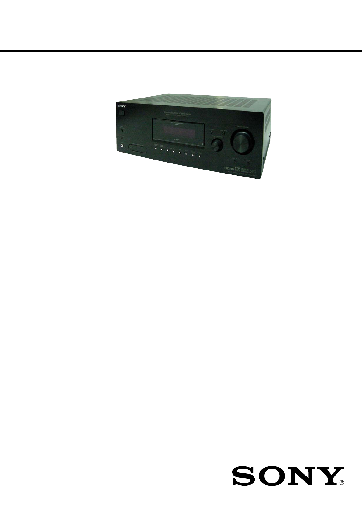
STR-K7000
SERVICE MANUAL
Ver. 1.0 2006. 03
• STR-K7000 is the multi
channel AV receiver
section in HT-7000DH.
Manufactured under license from Dolby Laboratories.
“Dolby”, “Pro Logic” and the double-D symbol are
trademarks of Dolby Laboratories.
“DTS” and “DTS Digital Surround” are trademarks
of Digital Theater Systems, Inc.
The XM name and related logos are registered
trademarks of XM Satellite Radio inc.
US Model
AUDIO POWER SPECIFICATIONS
POWER OUTPUT AND TOTAL HARMONIC
DISTORTION:
With 6 ohm loads, both channels driven, from
120 – 20,000 Hz; rated 90 watts per channel
minimum RMS power, with no more than
0.7 % total harmonic distortion from 250
milliwatts to rated output.
Amplifier section
Power Output
(6 ohms 1 kHz, THD 10 %)
FRONT
CENTER
SUR
1) Measured under the following conditions:
Area code Power requirements
US 120 V AC, 60 Hz
2) Depending on the sound field settings and the source,
there may be no sound output.
1)
2)
: 140 W/ch
2)
: 140 W
2)
: 140 W/ch
SPECIFICATIONS
Inputs (Analog)
MUL TI CH IN, Sensitivity: 800 mV
SA-CD/CD, Impedance: 50 kohms
MD/TAPE, DVD,
VIDEO 1, 2, 3
Inputs (Digital)
DVD (Coaxial) Sensitivity: —
Impedance: 75 kohms
VIDEO 1, 2 Sensitivity: —
(Optical) Impedance: —
Outputs (Analog)
MD/TAPE (OUT), Voltage: 800 mV
VIDEO 1 (AUDIO Impedance: 10 kohms
OUT)
SUBWOOFER Voltage: 2 V
Impedance: 1 kohms
Reproduction frequency range:
28 – 20,000 Hz
Tone
Gain levels ±6 dB, 1 dB step
– Continued on next page –
9-887-150-01
2006C04-1
© 2006. 03
MULTI CHANNEL AV RECEIVER
Sony Corporation
Home Audio Division
Published by Sony Techno Create Corporation
1
Page 2
STR-K7000
FM tuner section
Tuning range 87.5 – 108.0 MHz
Antenna FM wire antenna
Antenna terminals 75 ohms, unbalanced
Intermediate frequency 10.7 MHz
AM tuner section
Tuning range
With 10-kHz tuning scale: 530 – 1,710 kHz
With 9-kHz tuning scale: 531 – 1,710 kHz
Antenna Loop antenna
Intermediate frequency 450 kHz
3) You can change the AM tuning scale to 9 kHz or 10 kHz.
After tuning in any AM station, turn off the recei ver . While
holding down TUNING MODE, press ?/1. All preset
stations will be erased when you change the tuning scale.
To reset the scale to 10 kHz (or 9 kHz), repeat the
procedure.
3)
3)
Video section
Inputs/Outputs
Video: 1 Vp-p, 75 ohms
COMPONENT VIDEO: Y: 1 Vp-p, 75 ohms
PB/CB/B-Y: 0.7 Vp-p,
75 ohms
PR/CR/R-Y: 0.7 Vp-p,
75 ohms
80 MHz HD Pass Through
General
Power requirements
Area code Power requirements
US 120 V AC, 60 Hz
Power consumption
Area code Power consumption
US 170 W
Power consumption (during standby mode)
Dimensions (w/h/d) (Approx.)
Mass (Approx.) 8.0 kg (17 lb 11 oz)
Design and specifications are subject to change
without notice.
0.2 W
430 × 157.5 × 316 mm
(16 7/8 × 6 2/8 × 12 4/8
inches) including
projecting parts and
controls
SAFETY CHECK-OUT
After correcting the original service problem, perform the following safety check before releasing the set to the customer:
Check the antenna terminals, metal trim, “metallized” knobs, screws,
and all other exposed metal parts for AC leakage.
Check leakage as described below.
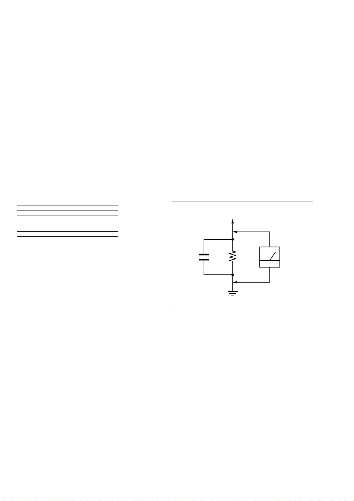
LEAKAGE TEST
The AC leakage from any exposed metal part to earth ground and
from all exposed metal parts to any exposed metal part having a
return to chassis, must not exceed 0.5 mA (500 microampers.).
Leakage current can be measured by any one of three methods.
1. A commercial leakage tester, such as the Simpson 229 or RCA
WT-540A. Follow the manufacturers’ instructions to use these
instruments.
2. A battery-operated AC milliammeter. The Data Precision 245
digital multimeter is suitable for this job.
3. Measuring the voltage drop across a resistor by means of a
VOM or battery-operated AC voltmeter. The “limit” indication is 0.75 V, so analog meters must have an accurate lowvoltage scale. The Simpson 250 and Sanwa SH-63Trd are examples of a passive VOM that is suitable. Nearly all battery
operated digital multimeters that have a 2 V AC range are suitable. (See Fig. A)
To Exposed Metal
Parts on Set
AC
1.5 k
0.15 µF
Ω
voltmeter
(0.75 V)
Earth Ground
Fig. A. Using an AC voltmeter to check AC leakage.
SAFETY-RELATED COMPONENT WARNING!!
COMPONENTS IDENTIFIED BY MARK 0 OR DOTTED LINE
WITH MARK 0 ON THE SCHEMATIC DIAGRAMS AND IN
THE PARTS LIST ARE CRITICAL TO SAFE OPERATION.
REPLACE THESE COMPONENTS WITH SONY P ARTS WHOSE
PART NUMBERS APPEAR AS SHOWN IN THIS MANUAL OR
IN SUPPLEMENTS PUBLISHED BY SONY.
2
Page 3

TABLE OF CONTENTS
1. GENERAL
Description and location of parts............................................. 4
2. DISASSEMBL Y
2-1. Case ..................................................................................... 7
2-2. Front Panel Section ............................................................. 8
2-3. Back Panel Section.............................................................. 8
2-4. DIGITAL Board .................................................................. 9
2-5. MAIN Board Section .......................................................... 9
2-6. STANDBY Board ............................................................. 10
3. TEST MODE ..................................................................... 11
4. DIAGRAMS
4-1. Circuit Boards Location .................................................... 12
4-2. Block Diagram – Tuner/Audio Section –.......................... 14
4-3. Block Diagram – Digital Section – ................................... 15
4-4. Block Diagram – Video Section – .....................................16
4-5. Block Diagram – XM Section –........................................ 17
4-6. Block Diagram – Key/Display Section – .......................... 18
4-7. Block Diagram – Power Section – .................................... 19
4-8. Printed Wiring Boards – Main Section – .......................... 20
4-9. Schematic Diagram – Main Section (1/3) – ...................... 21
4-10. Schematic Diagram – Main Section (2/3) – ...................... 22
4-11. Schematic Diagram – Main Section (3/3) – ...................... 23
4-12. Printed Wiring Board – Digital Section (1/2) – ................ 24
4-13. Printed Wiring Board – Digital Section (2/2) – ................ 25
4-14. Schematic Diagram – Digital Section (1/5) – ................... 26
4-15. Schematic Diagram – Digital Section (2/5) – ................... 27
4-16. Schematic Diagram – Digital Section (3/5) – ................... 28
4-17. Schematic Diagram – Digital Section (4/5) – ................... 29
4-18. Schematic Diagram – Digital Section (5/5) – ................... 30
4-19. Printed Wiring Boards
– Front B/Center Speaker Section –.................................. 31
4-20. Schematic Diagram
– Front B/Center Speaker Section –.................................. 32
4-21. Printed Wiring Boards – Video Section – ......................... 33
4-22. Schematic Diagram – Video Section –.............................. 34
4-23. Printed Wiring Board – HDMI Section – ..........................35
4-24. Schematic Diagram – HDMI Section – ............................ 36
4-25. Printed Wiring Board – XM Section – .............................. 37
4-26. Schematic Diagram – XM Section –................................. 38
4-27. Printed Wiring Board – ADCC Section – ......................... 39
4-28. Schematic Diagram – ADCC Section – ............................ 39
4-29. Printed Wiring Boards – Display Section – ...................... 40
4-30. Schematic Diagram – Display Section –........................... 41
4-31. Printed Wiring Board – Power Section – .......................... 42
4-32. Schematic Diagram – Power Section – ............................. 43
STR-K7000
5. EXPLODED VIEWS
5-1. Case Section ...................................................................... 53
5-2. Front Panel Section ........................................................... 54
5-3. Back Panel Section............................................................ 55
5-4. Chassis Section ................................................................. 56
6. ELECTRICAL PARTS LIST ........................................ 57
3
Page 4
STR-K7000
3 6 84 75
12
8
SECTION 1
GENERAL
This section is extracted
from instruction manual.
Getting Started
Description and location of parts
Receiver
Front panel
?/1
SPEAKERS
(OFF/A/B/A+B)
AUTO CAL MIC
VIDEO 3 IN/PORTABLE AV IN
PHONES
VIDEO L AUDIO R
ql
P
U
S
H
To rem ove the cover
Press PUSH.
When you remove the cover, keep it out of
reach from children.
MULTI CHANNEL DECODING
MEMORY/
TUNING
ENTER
MODE
TUNING 2CH A.F.D. MOVIE MUSIC MULTI CH IN MUTING
Name Function
A ?/1 Press to turn the receiver on
B SPEAKERS
(OFF/A/B/A+B)
C Display The current status of the
D MULTI
CHANNEL
DECODING
lamp
DISPLAY INPUT MODE
MASTER VOLUME
INPUT SELECTOR
q; 9qaqsqdw; qfqgqhqjqk
or off (page 29, 37, 38, 53,
79).
Press to select OFF, A, B,
A+B of the front speakers
(page 30).
selected component or a list
of selectable items appears
here (page 7).
Lights up when multi
channel audio is decoded
(page 38).
continued
Name Function
Getting Started
US
5
E Remote sensor Receives signals from
F DISPLAY Press to select information
G INPUT MODE Press to select the input
H MASTER
VOLUME
I MUTING Press to mute the sound
J MULTI CH I N Press to select the audio
K INPUT
SELECTOR
L MOVIE,
MUSIC
M A.F.D. Press to select A.F.D.
N 2CH Press to select 2CH
O TUNING +/– Press to scan a station
P TUNING MODE Press to select the tuning
Q MEMORY/ENTER Press to store a station or
US
6
remote commander.
displayed on the display
(page 67).
mode when the same
components are connected
to both digital and analog
jacks (page 64).
Turn to adjust the volume
level of all speakers at the
same time (page 34, 35,
37, 38).
(page 35).
directly from the
components connected to
the MULTI CH IN jacks
(page 35).
Turn to select the input
source to playback (page
35, 37, 38, 54, 56, 64, 66,
68).
Press to select sound fields
(MOVIE, MUSIC) (page
50).
mode (page 48).
STEREO mode (page 52,
53).
(page 54, 55).
mode (page 56, 79).
enter the selection when
selecting the settings
(page 29).
Name Function
R VIDEO 3 IN/
PORTABLE AV IN
jacks
S AUTO CAL MIC
jack
T PHONES jack Connects to a headphone
To conn ect a camcorder or
video game (page 27, 35).
Connects to the supplied
ECM-AC2 optimizer
microphone for the Auto
Calibration function (page
31).
(page 75).
About the indicators on the display
21435
SP A
DIGITAL
;
LFE
SW
SP B
qg
is output from the SUB
WOOFER jack.
played back contains an LFE
(Low Frequency Effect)
channel and the LFE channel
signal is actually being
reproduced.
speaker system used. However,
these indicators do not l ight up
if the speaker output is t u r ned
off or if a headphone is
connected.
signals are input.
Note
When playing a Dolby Digital
format disc, be sure that you
have made digital connections
and that INPUT MODE is not
set to “ANALOG” (page 64).
Lights up when the receiver
applies Pro Logic processing to
2 channel signals in order to
output the center and surround
channel signals. “; PRO
LOGIC II” lights up when the
Pro Logic II Movie or Music
decoder is activated.
Note
Dolby Pro Logic and Dolby Pro
Logic II decoding do not
function for DTS format
signals.
SLEEP OPT COAX HDMI
qf
L C R
SLSSR
Name Function
A SW Lights up when the audio signal
B LFE Lights up when the disc being
C SP A/SP B Lights up according to the
D ;DIGITAL Lights up when Dolby Digital
E ;PRO
LOGIC (II)
;
PRO LOGIC II
qsqd
6
DTS
qa q;
CAT
STEREO MONOD.RANGE
9
Name Function
F DTS Lights up when DTS signals are
G MEMORY Lights up when a memory
H Preset
station
indicators
I Tuner
indicators
J D.RANGE Lights up when dynamic range
K HDMI Flashes when you select
L COAX Lights up when INPUT MODE
input.
Note
When playing a DTS format
disc, be sure that you have made
digital connections and that
INPUT MODE is not set to
“ANALOG ” (page 64).
function, such as Preset
Memory (page 55), etc., is
activated.
Lights up when using the
receiver to tune i n radi o stations
you have preset. For details on
presetting radio stations, see
page 55.
Lights up when using the
receiver to tune i n radi o stations
(page 53), etc.
compression is activated (page
40).
“HDMI A.” in the VIDEO
menu (page 65).
is set to “A UTO” a nd the source
signal is a digital signal being
input through the COAXIAL
jack, or when INPUT MODE is
set to “COAX IN” (page 64).
7
MEMORY
Getting Started
Name Function
M OPT Lights up when INPUT MODE
N SLEEP Lights up when the sleep timer
O Playback
channel
indicators
L
R
C
SL
SR
S
is set to “A UTO” and the source
signal is a digital signal being
input through the OPTICAL
jack, or when INPUT MODE is
set to “OPT IN” (page 64).
is activated (page 67).
The letters (L, C, R, etc.)
indicate the channels being
played back. The boxes around
the letters vary to show ho w the
receiver downmixes the source
sound.
Front Left
Front Right
Center (monaural)
Surround Left
Surround Right
Surround (monaural or the
surround components obtained
by Pro Logic processing)
Example:
Recording format (Front/
Surround): 3/2.1
Sound Field: A.F.D. AUTO
SW
L C R
SL SR
continued
US
7
US
8
4
Page 5
STR-K7000
q
q
Rear panel
1 23
DVD IN
VIDEO 2 IN
OUT ININ
MD/TAPE
ASSIGNABLE
VIDEO IN
L
R
AUDIO IN
DVD
a)
a)
MONITOR OUT
HDMI
VIDEO IN
VIDEO OUT
L
R
AUDIO IN
AUDIO OUT
VIDEO 1
VIDEO 2
5 46
Connects to a DVD
player, etc. The
COAXIAL jack
provides a better
quality of loud
sound (page 23,
26).
Connects to a DVD
player, or a satellite
tuner. The image
and the sound are
output to a TV or a
projector (page
25).
Connects the video
and audio jacks of
a VCR or a DVD
player (page 22,
23, 24, 26, 27).
DIGITAL
OPTICAL
VIDEO 1
ANTENNA
IN
VIDEO 2
DVD
COAXIAL
XM
IN
AM
IN
L
R
SA-CD/CD
A DIGITAL INPUT section
OPTICAL
IN jack
COAXIAL IN
jack
HDMI IN/
MONITOR
OUT jack
B VIDEO/AUDIO INPUT/OUTPUT
section
AUDIO IN/
White (L)
OUT jack
Red (R)
VIDEO IN/
Yellow
OUT jack
E AUDIO INPUT/OUTPUT section
Getting Started
COMPONENT VIDEO
ASSIGNABLE
MONITOR
DVDINVIDEO 2INMONITOR
VIDEO IN
VIDEO OUT
L
L
R
R
AUDIO IN
FRONT
SURROUND
MULTI CH IN
CENTER
Y
+
–
PB/C
B
/BñY
SPEAKERS
P
R/CR
/RñY
OUT
L
L
+–+
R
SURROUND FRONT A
SPEAKERS
COMPONENT
VIDEO
INPUT/
OUTPUT
jack
–
R
a)
AUDIO
OUT
CENTER
SUB
WOOFER
SUB
WOOFER
C COMPONENT VIDEO INPUT/
OUTPUT section
Green
Blue
Red
D SPEAKER section
LR
LR
FRONT B
SPEAKERS
Connects to a DVD
player, TV, or a
satellite tuner. You
can enjoy high
quality image
(page 22, 24, 26).
Connects to
speakers (page 16).
Connects to sub
woofer (page 16).
continued
F ANTENNA section
a)
US
9
10
AUDI O IN/
White (L)
OUT jack
Red (R)
MULTI
White (L)
CHANNEL
INPUT jack
Red (R)
Black
FM
ANTENNA
AM
ANTENNA
XM Connects to the
You ca n watch the selected input image when you
connect the MONITOR OUT jack to a TV monitor
(page 22).
US
Connects to an MD
deck or CD player,
etc. (page 20).
Connects to a
Super Audio CD
player or DVD
player which has
an analog audio
jack for 5.1
channel sound
(page 19).
Connects to the
FM wire antenna
supplied with this
receiver (page 28).
Connects to the
AM loop antenna
supplied with this
receiver (page 28).
XM connect-andPlay antenna (not
supplied with this
receiver) (page
58).
Remote commander
You can use t he supplied remote RM-AAP012
to operate the receiver and to control the Sony
audio/video components that the remote is
assigned to operate. You can also program the
remote to control non-Sony audio/video
components. For details, see “Programmi ng
the remote” (page 69).
wl
TV ?/1 AV ?/1
P
RM SET UP
wk
TV ?/1
(on/standby)
switch
wj
wh
wg
wf
wd
ws
wa
w;
ql
qk
SYSTEM STANDBY
VIDEO1 VIDEO2
MD/TAPE SA-CD/CD TUNER
2CH
A.F.D.
123
CATEGORY
456
AUDIO
ANGLE
TUNING
789
SUBTITLEMEMORY ENTER
>
.
>10/11 12
0/10
D.TUNING DISC ALT
M
m
ANT
CLEAR
H
TOP MENU/
GUIDE
F
G
f
DISPLAY
TV VOL TV CH
VIDEO3 DVD
SEARCH MODE
X
AV MENU
g
RETURN/EXIT
qj
h
Name Function
A AV ?/1 Press to turn on or off the
audio/video components that
the remote is programmed to
operate.
If you press ?/1 (B) at the
same time, it will turn off the
receiver and other
components (SYSTEM
STANDBY).
Note
The function of the AV ?/1
switch changes automatically
each time you press the input
buttons (wj).
AV ?/1
1
(on/standby)
?/1
switch
?/1
(on/standby)
2
switch
SLEEP
AUX
MULTI CH
3
MOVIE
MUSIC
4
DUAL
CATEGORY
MONO
MODE
5
JUMP/
PRESET/
TIME
CH/D.SKIP
6
-
7
8
x
9
MUTING
q;
MASTER
VOL
qa
O
TV/
AMP
VIDEO
MENU
qs
AUTO
qd
WIDE
CAL
qf
g
Name Function
B ?/1 Press to turn the receiver on or
SLEEP Press ALT (G) and then press
C MULTI CH Press to select the audio directly
D MUSIC Press to select sound fields
E CATEGORY
MODE
F PRESET/
CH/D.SKIP
+/–
G ALT Press to light up the button. It
H -/-- Press to select the channel entry
DISC Press to select a disc directly of
SEARCH
MODE
I x Press to stop playback of the
off.
To t urn off all components,
press ?/1 and AV ?/1 (A) at
the same time (SYSTEM
STANDBY).
SLEEP to activate the Sleep
Timer function and the duration
which the receiver turns off
automatically.
from the components connected
to the MULTI CH IN jacks.
(MUSIC).
Press to select the category
mode for XM Radio.
Press to
–select preset stations.
–select preset channels of the
TV, VCR, satellite tuner, Bluray disc recorder, or hard disc
recorder.
–skip disc of the CD player,
VCD player, DVD player,
MD deck, or LD player
(multi-disc changer only).
changes the remote key
function to activate the buttons
with orange printing.
mode, either one or two digit of
the TV, Blu-ray disc recorder,
hard disc recorder, PSX, or
satellite tuner.
the CD player or VCD player
(multi-disc changer only).
Press to select the searching
mode or unit for search (tracks,
index, etc.) of the DVD player.
VCR, CD player, VCD player,
LD player, DVD player, MD
deck, DAT deck, tape deck, Bluray disc recorder, hard disc
recorder, or PSX.
Name Function
J MUTING Press to mute the sound.
K MASTER
VOL +
L AMP ME NU Press to display the menu of the
M TV/VIDEO Press to select the input signal
N AUTO CAL Press to activate the Auto
O WIDE Press ALT (G) and then press
P TV CH +
Q TV VOL
+
R RETURN/
EXIT O
S DISPLAY Press to select infor mation
T Control
buttons
U TOP MENU/
GUIDE
Press to adjust the volume le vel
a)
/–
of all speakers at the same time.
receiver. Then, use the control
buttons to perform menu
operations.
(TV input or video input).
Calibration function.
WIDE to select the wide picture
mode.
a)
/– Press to select preset TV
channels.
Press to adjust the TV volume
a)
/–
level.
Press to
–return to the previous menu.
–exit the menu whi le the menu
displayed on the TV screen of
the TV, VCR, VCD player, LD
player, DVD pla yer , CD play er ,
MD deck, Blu-ray disc
recorder, hard disc recorder,
PSX, or satellite tuner.
After pressing AMP MENU
(L), TOP MENU/GUIDE
(U), or AV MENU (V), press
the control button V, v, B or b
to select the settings. When you
press TOP MENU/GUIDE or
AV MENU, press the control
button to enter the selection.
Press to display the
–DVD title.
–menu or on-screen guid e of
Then, use the control b utton s to
perform menu operation.
or on-screen guide of the
VCD player, LD player, DVD
player, Blu-ray disc recorder,
hard disc recorder, PSX, or
satellite tuner is displayed on
the TV screen.
the satellite tuner, Blu-ray
disc recorder, hard disc
recorder, or PSX on the TV
screen.
continued
11
Name Function
Getting Started
US
V AV MENU Press to display the menus of the
W H
X X Press to pause playback or
Y m/M Press to
US
12
VCR, DVD player, satellite
tuner, Blu-ray disc recorder,
hard disc recorder, or PSX on the
TV screen. Then, use the control
buttons to perform menu
operations.
a)
Press to start playback of the
VCR, CD player, VCD player,
LD player, DVD player, MD
deck, DAT deck, tape deck, Bluray disc recorder, hard disc
recorder, or PSX.
recording of the VCR, CD
player, VCD player, LD player,
DVD player, MD deck, DAT
deck, tape deck, Blu-ray disc
recorder, hard disc recorder, or
PSX. (Also starts recording with
components in recording
standby.)
–search tracks in the forward/
backward direction of the CD
player, VCD player, DVD
player, LD player, MD de ck,
Blu-ray disc recorder, hard
disc recorder, or PSX.
–fast forward/rewind of the
D. TUNING Press to enter dire ct tuning
ANT Press ALT (G) and then press
CLEAR Press ALT (G) and then press
VCR, DAT deck, or tape deck.
mode.
ANT to select the signal to be
output from the antenna terminal
of the VCR or satellite tuner ( TV
signal or video signal).
CLEAR to
–clear a mistake when you press
the incorrect numeric button.
–return to continuous playback,
etc. of the CD player, DVD
player, Blu-ray disc recorder,
PSX, or satellite tuner.
Name Function
Z TUNING +/– Press to scan a station.
./> Press to skip tracks of the
2CH Press to select 2CH STEREO
A.F.D. Press to select A.F.D. mode.
MOVIE Press to select sound fields
CATEGORY
+/–
DUAL MONO Press to select the language
AUDIO Press to change the sound to
ANGLE Press to select the viewing
JUMP/TIME Press to
MEMORY Press MEMORY to store a
SUBTITLE Press ALT (G) and then press
ENTER Press ALT (G) and then press
VCR, CD player, VCD player,
LD player, DVD player, MD
deck, DAT deck, tape deck,
Blu-ray disc recorder, hard
disc recorder, or PSX.
mode.
(MOVIE).
Press to select the category for
XM Radio.
you want during digital
broadcast.
Multiplex, Bilingual or Multi
channel TV sound of the TV,
VCR, DVD player, satellite
tuner, Blu-ray disc recorder,
hard disc recorder, or PSX.
angle or change the angles of
the DVD player or Blu-ray
disc recorder.
–toggle between the previous
and the current channels of
the satellite tuner, TV, or
Blu-ray disc recorder.
–show the time or display the
playing time of a disc, etc. of
the CD player, MD deck,
VCD player, or DVD player.
station.
SUBTITLE to change the
subtitles of the DVD player.
ENTER to enter the value
after selecting a channel, disc
or track using the numeric
buttons.
5
Page 6
STR-K7000
Name Function
wh Numeric
buttons
>10/11 Press ALT (G) and then press
wj Input buttons Press one of the buttons to
Press ALT (G) and then pres s
the numeric buttons to
–preset/tune to preset
stations.
–select track numbers of the
CD player, VCD player, LD
player, DVD player, MD
deck, DAT deck, or tape
deck. Press 0/10 to select
track number 10.
–select channel numbers of
the TV, VCR, satellite tu ner,
Blu-ray disc recorder, hard
disc recorder, or PSX.
>10/11 to select track
numbers over 10 of the CD
player, VCD player, LD
player, MD deck, tape deck,
TV, VCR, Blu-ray disc
recorder, hard disc recorder,
PSX, or satellite tuner.
select the component you
want to use. When you press
any of the input buttons, the
receiver turns on. The buttons
are factory assigned to control
Sony components as follows.
You c an program the remote
to control non-Sony
components following the
steps in “Programming the
remote” on page 69.
Button Assigned Sony
component
VIDEO1 VCR (VTR mode 3)
VIDEO2 VCR (VTR mode 1)
VIDEO3 VCR (VTR mode 2)
DVDDVD player
MD/TAPE MD deck
SA-CD/CD Super Audio CD/CD
player
TUNER Built-in tuner
AUXNot assigned
Name Function
wk TV ?/1 Press to turn the TV on or off.
wl RM SET UP Press to set up the remote.
a)
The MASTER VOL +, TV VOL +, TV CH + and
H buttons have tactile dot s. Use the tactile dots as
references when operating the re ceiver.
Notes
•Some functions explained in this section may not
work depending on the model.
•The above explanation is intended to serve as an
example only. Therefore, depending on the
component, the above operation may not be
possible or may operate differently than described.
•The 12 button on the remote is not available for
receiver operation.
Getting Started
US
13
6
Page 7
SECTION 2
)
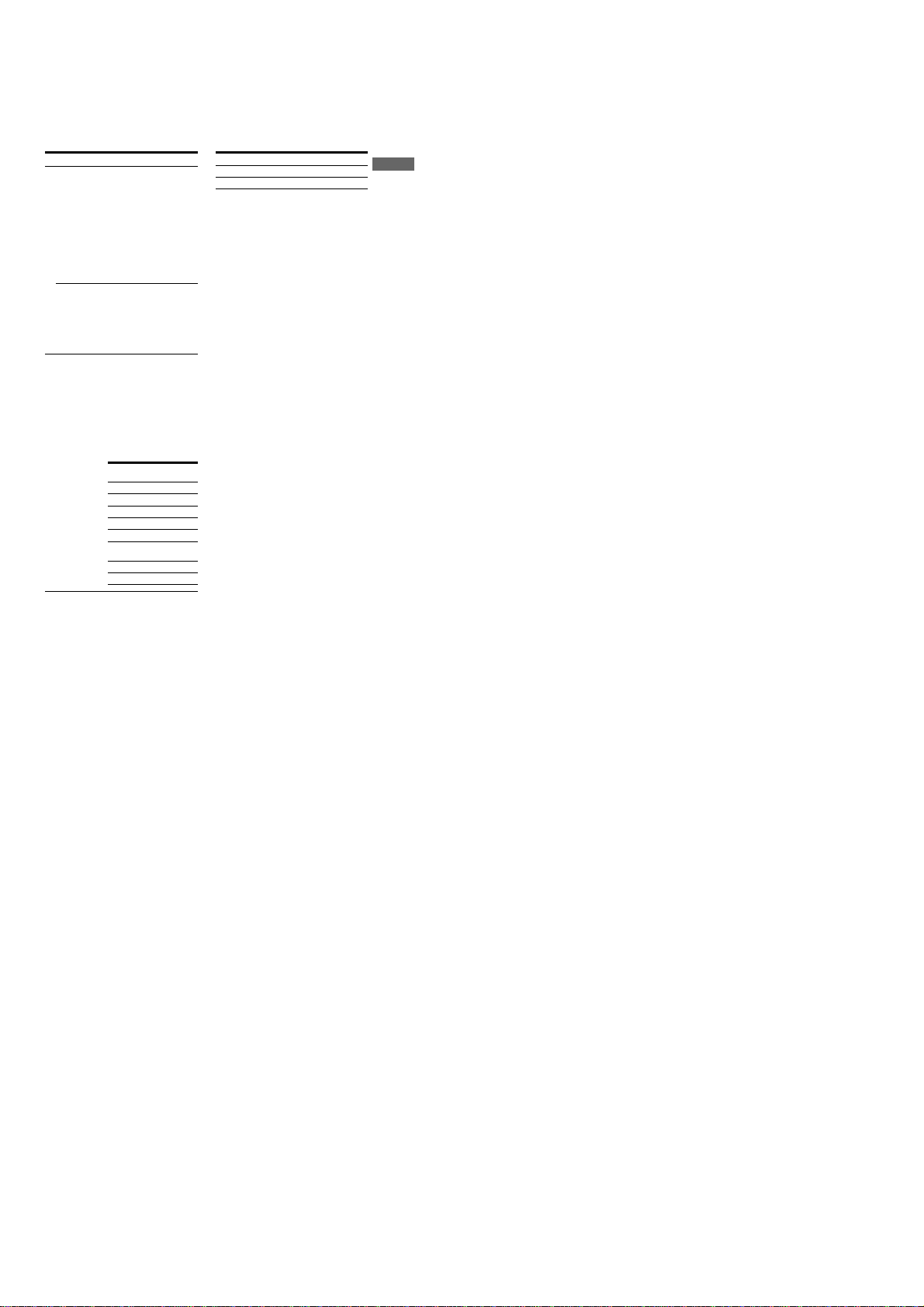
DISASSEMBLY
Note : This set can be disassemble according to the following sequence.
SET
2-1. CASE
(Page 7)
STR-K7000
2-2. FRONT PANEL SECTION
(Page 8)
2-6. STANDBY BOARD
(Page 10)
2-3. BACK PANEL SECTION
(Page 8)
2-4. DIGITAL BOARD
(Page 9)
2-5. MAIN BOARD SECTION
(Page 9)
Note : Follow the disassembly procedure in the numerical order given.
2-1. CASE
2
two
screws
(case 3 TP2)
3
two
screws
(+BVTP 3
×
8
1
two
(case 3 TP2)
4
screws
case
7
Page 8
STR-K7000
)
)
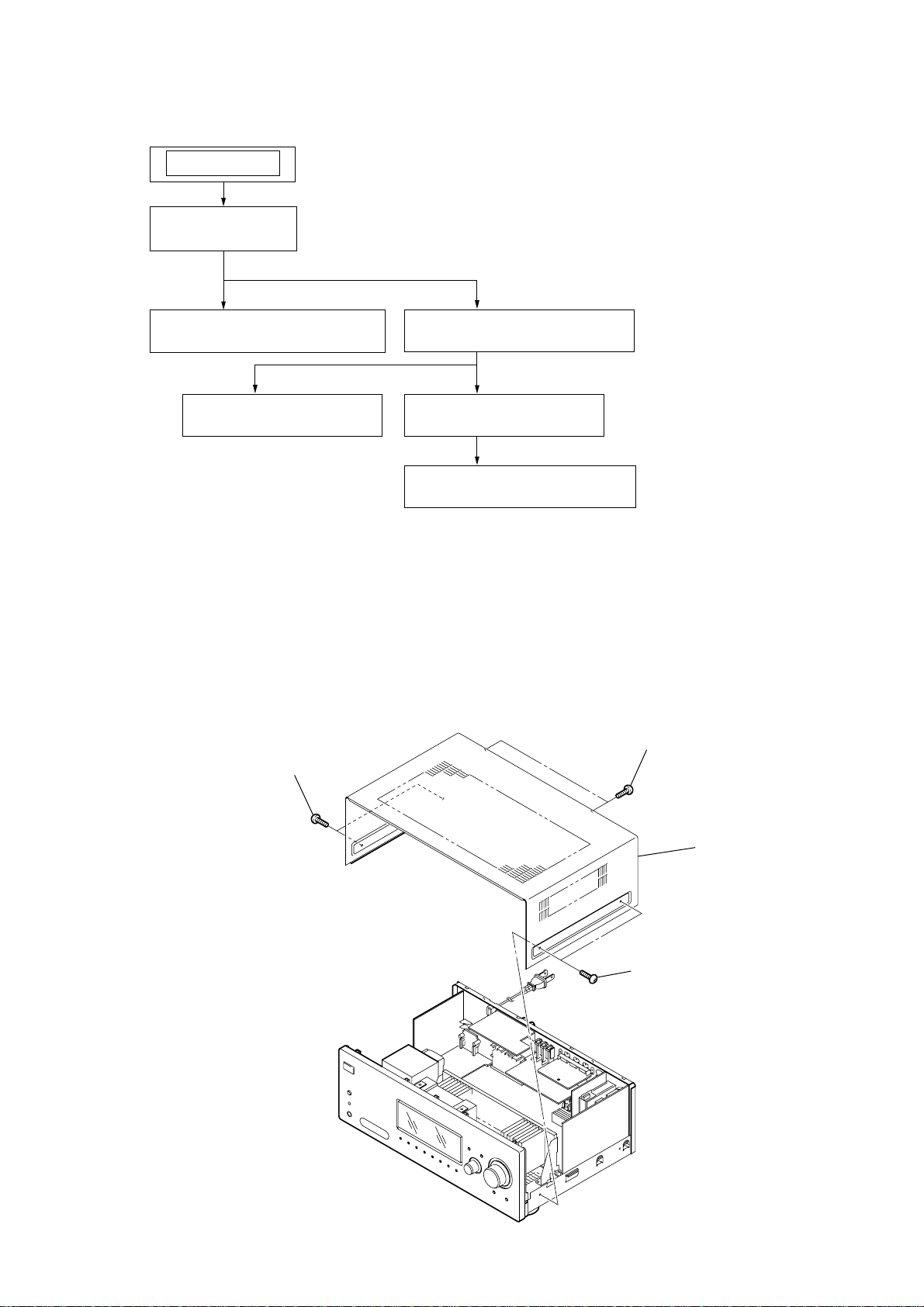
2-2. FRONT P ANEL SECTION
1
CNP2000 (4P)
2
CNP791 (4P)
6
two
screws
(+BVTP 3
×
8)
4
CNP202 (3P)
5
CNP503 (3P
8
front panel section
2-3. BACK PANEL SECTION
1
CNP901 (2P)
2
CNP806 (3P)
0
screw
(+BVTP 3
7
CNP503 (4P)
×
8)
3
7
five
screws
(+BVTP 3
8
CN103 (2P)
9
CNP203 (3P)
qa
(+BVTP 3
CNS505 (23 core)
×
8)
two
screws
×
8)
qs
two
screws
(+BVTP 3
×
qd
five
(+BVTP 3
3
CNS509 (17 core)
8)
screws
×
8)
qf
three
(+BVTP 3
screws
×
8
qg
four
screws
5
CNS503 (9 core)
4
CNS508 (11 core)
6
CN504 (5 core)
(+BVTP 3
qh
back panel section
×
8)
8
Page 9
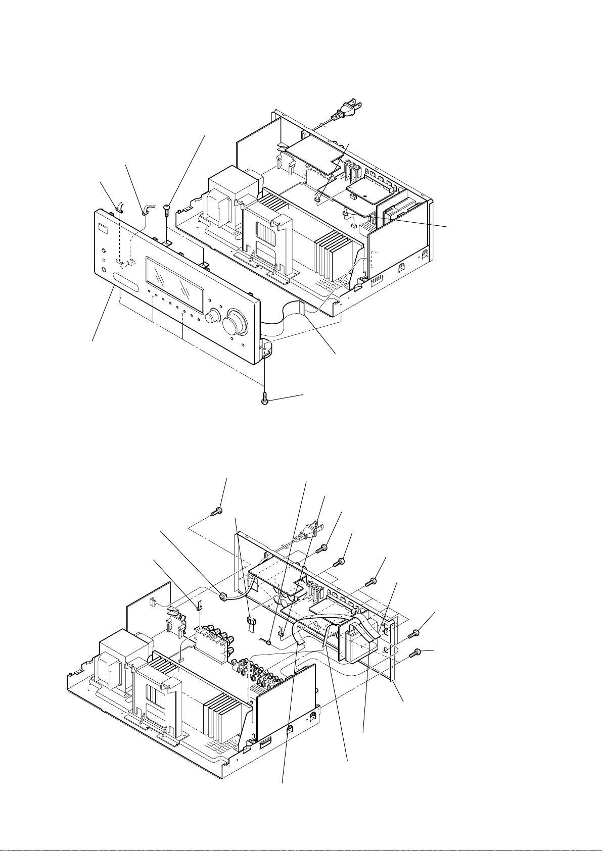
2-4. DIGIT AL BOARD
d
3
CNP504 (7P)
2
CNP503 (5P)
1
CNP505 (10P)
5
4
screw
(+BVTP 3
STR-K7000
DIGITAL boar
×
8)
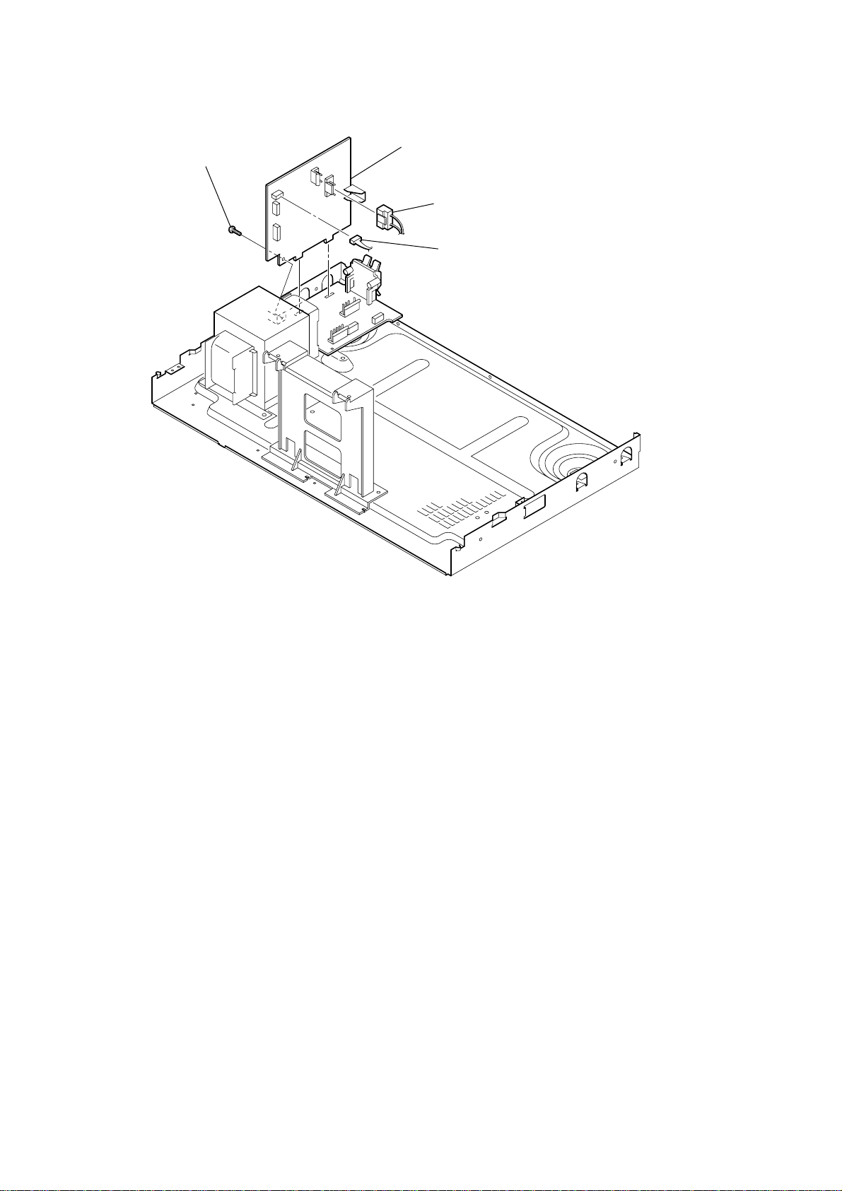
2-5. MAIN BOARD SECTION
3
CNP801 (5P)
7
two
(+BV3 (3
1
CNP600 (5P)
8
screw
(+BV3 (3
screws
-CR)
2
CNP601 (4P)
4
-CR)
)
CNP802 (5P)
)
5
CNP801 (3P)
6
two
screws
(+BV3 (3
-CR)
)
9
MAIN board section
9
Page 10
STR-K7000
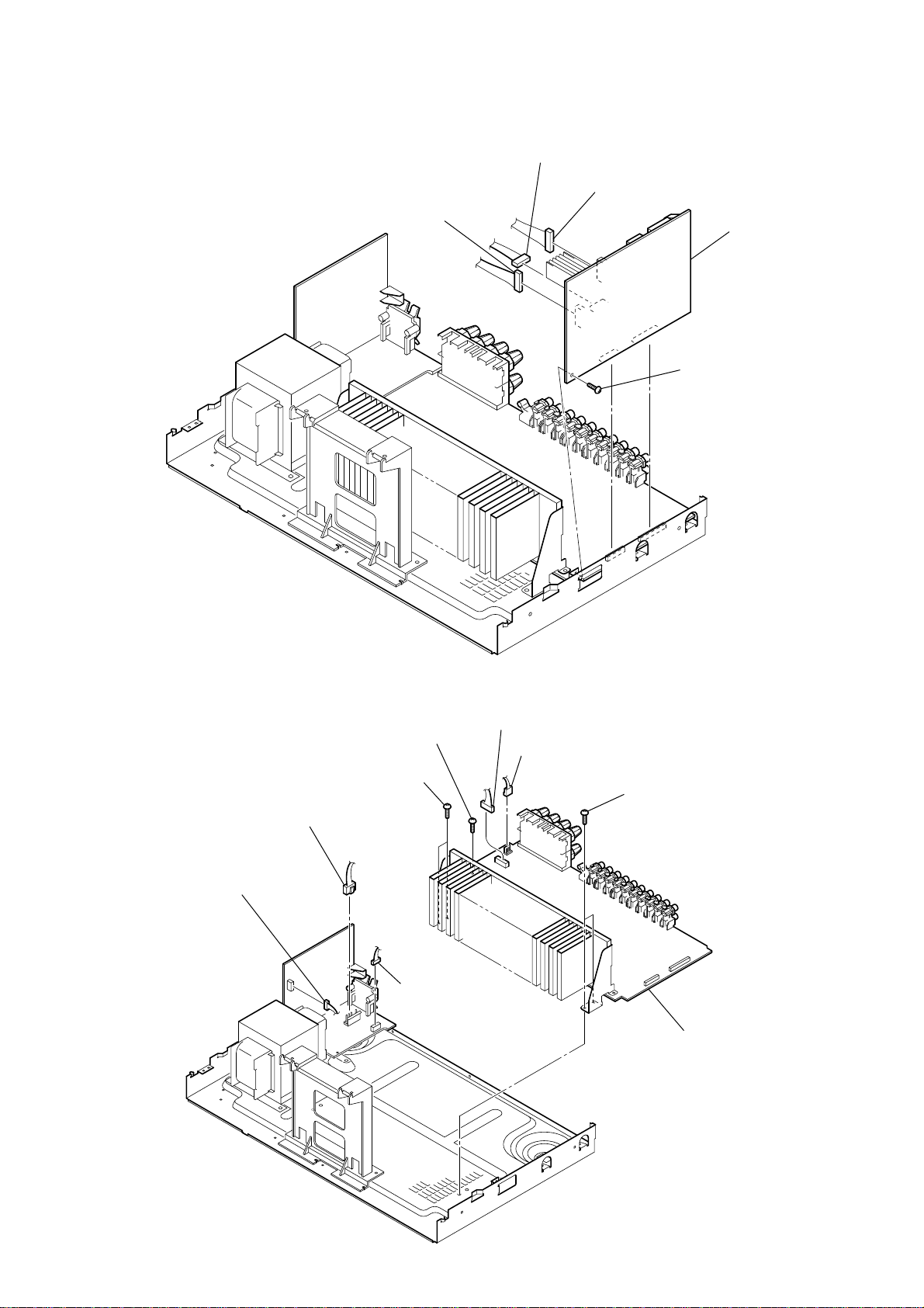
2-6. STANDBY BOARD
3
screw
(+BVTP 3
×
4
STANDBY board
8)
1
CNP902 (2P)
2
CNP804 (3P)
10
Page 11
SECTION 3
TEST MODE
STR-K7000
FACTORY PRESET MODE
* All preset contents are reset to the default setting.
* Procedure:
While depressing the [SPEAKERS $OFF/A/B/A+B%] and the
[MOVIE] buttons simultaneously, press the
?/1 button to turn
on the main power.
The message “FA CT OR Y” appears for a moment and the present
contents are reset to the default values.
AM CHANNEL STEP 9 kHz/10 kHz SELECTION
MODE
* Either the 9 kHz step or 10 kHz step can be selected for the AM
channel step.
* Procedure:
Turn the [INPUT SELECTOR] control to set AM and press the
?/1 button to turn off the main power.
While depressing the [TUNING MODE] button, press the ?/1
button to turn on the main power.
Either the message “9k STEP” or “10k STEP” appears for a
moment and select the desired step.
VACUUM FLUORESCENT DISPLAY TEST MODE
* All fluorescent segments are tested.
When this test is activated, all segments light on at the same
time, then each segment lights on one after another.
* Procedure:
While depressing the [TUNING MODE] and the [DISPLAY] buttons simultaneously, press the ?/1 button to turn on the main
power.
1. ALL segments light on.
dB
k Hz
m ft.
MHz
dB
MEMORY
A.DIRECT
MEMORY
Hz
ft.
SP A
D
D
D
D
LFE
SW
CR
L
SL S SR
SBL SB SBR
DIGITALEX PRO LOGIC II x DTS-ES NEO:6 AAC CAT RDS
SP B SLEEP OPT COAX HDMI 96/24
D.RANGE EQ STEREO MONO
[MULTI CHANNEL DECODING] LED light on.
2. Turn the [INPUT SELECTOR] control, confirm display.
A
LFE
SW
L
R
S
SB
EX DTSII NEO:6 CAT
SLEEP COAX 96/24
D.RANGE
STEREO
SOUND FIELD CLEAR MODE
* The preset sound field is cleared when this mode is activated.
Use this mode before returning the product to clients upon
completion of repair.
* Procedure:
While depressing the [2CH] button, press the ?/1 button to turn
on the main power.
The message “S.F. CLR.” appear s for a moment and initialization is performed.
SOFTWARE VERSION DISPLAY MODE
* The software version is displayed.
* Procedure:
While depressing the [SPEAKERS $OFF/A/B/A+B%] and the
[DISPLAY] buttons simultaneously, press the ?/1 button to turn
on the main power.
The model name, destination and the software version are displayed for a moment.
KEY CHECK MODE
* Button check
* Procedure:
While depressing the [SPEAKERS $OFF/A/B/A+B%] and the [2CH]
buttons simultaneously , press the ?/1 button to turn on the main
power.
Either the message “REST 13” appears.
Every pressing of any button other than the ?/1 counts down
the buttons. The buttons which are already counted once are not
counted again. When all buttons are pr essed “REST 00” appears.
COMMAND MODE SELECTION MODE
* The command mode (AV1 or AV2) of the remote commander
can be selected.
* Procedure:
While depressing the [INPUT MODE] button, press the
ton to turn on the main power.
Either the message “C.MODE.AV 1” or “C.MODE.AV 2” appears for a moment and select the desired mode.
?/1 but-
3. Turn the [INPUT SELECTOR] control, confirm display.
SP
D
D
D
D
DIGITAL xPRO LOGIC -ES AAC RDS
SP B OPT HDMI
C
SL SR
SBL SBR
EQ MONO
k
m
MHz
A.DIRECT
[MULTI CHANNEL DECODING] LED light on.
4. Turn the [INPUT SELECTOR] control, all segments and all LEDs
light off.
11
Page 12
STR-K7000
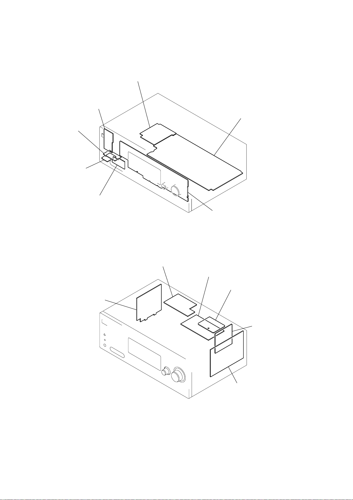
4-1. CIRCUIT BOARDS LOCATION
POWER board
ADCC board
HEADPHONE board
SECTION 4
DIAGRAMS
SPEAKER B board
MAIN board
VIDEO3 board
STANDBY board
DISPLAY board
SPEAKER C/SB board
VIDEO board
HDMI SW board
XM board
12
DIGITAL board
Page 13
STR-K7000
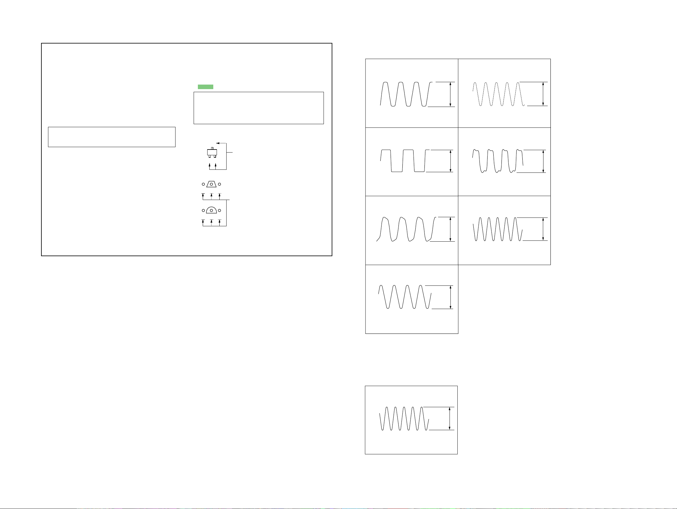
1
IC1301 qd (CKOUT)
2.1 Vp-p
1.8 Vp-p
1V/DIV, 50nsec/DIV
3
IC1301 wa (XOUT)
1V/DIV, 50nsec/DIV
4
IC1501 9 (MCLK1)
0.6 Vp-p
1V/DIV, 50nsec/DIV
2
IC1301 qf (BCK)
2.4 Vp-p
1V/DIV, 0.2µsec/DIV
13.9 MHz
12.288 MHz
3.07 MHz
12.288 MHz
5
IC1501 qs (MCLK2)
1.1 Vp-p
2.2 Vp-p
1V/DIV, 50nsec/DIV
7
IC1101 id (X1)
1V/DIV, 50nsec/DIV
6
IC1501 qf (SCKOUT)
2.5 Vp-p
1V/DIV, 50nsec/DIV
24 MHz
12.288 MHz
13.9 MHz
THIS NOTE IS COMMON FOR PRINTED WIRING BOARDS AND SCHEMATIC DIAGRAMS.
(In addition to this, the necessary note is printed in each block.)
for schematic diagram:
• All capacitors are in µF unless otherwise noted. (p: pF)
50 WV or less are not indicated except for electrolytics
and tantalums.
• All resistors are in Ω and 1/
specified.
f
•
• 2 : nonflammable resistor.
• 5 : fusible resistor.
• C : panel designation.
Note: The components identified by mark 0 or dotted line
• A : B+ Line.
• B : B– Line.
•Voltage and waveforms are dc with respect to ground
•Voltages are taken with a VOM (Input impedance 10 MΩ).
•Waveforms are taken with a oscilloscope.
• Circled numbers refer to waveforms.
• Signal path.
: internal component.
with mark 0 are critical for safety.
Replace only with part number specified.
under no-signal (detuned) conditions.
no mark : FM
Voltage variations may be noted due to normal production tolerances.
Voltage variations may be noted due to normal production tolerances.
F : TUNER (FM/AM)
L : VIDEO (AUDIO)
I : VIDEO
J : CD (ANALOG)
c : CD (DIGITAL)
4
W or less unless otherwise
for printed wiring boards:
• X : parts extracted from the component side.
f
•
• : Pattern from the side which enables seeing.
Caution:
Pattern face side: Parts on the pattern face side seen from the
(Side B) pattern face are indicated.
Parts face side: Parts on the parts face side seen from the
(Side A) parts face are indicated.
: internal component.
C
Q
B
E
Q
BCE
Q
B
C
E
These are omitted.
These are omitted.
• Waveforms
— DIGITAL Board —
— XM Board —
1
IC102 wh (OSCOUT)
45.158 MHz
1V/DIV, 50nsec/DIV
0.8 Vp-p
STR-K7000
13 13
Page 14
STR-K7000
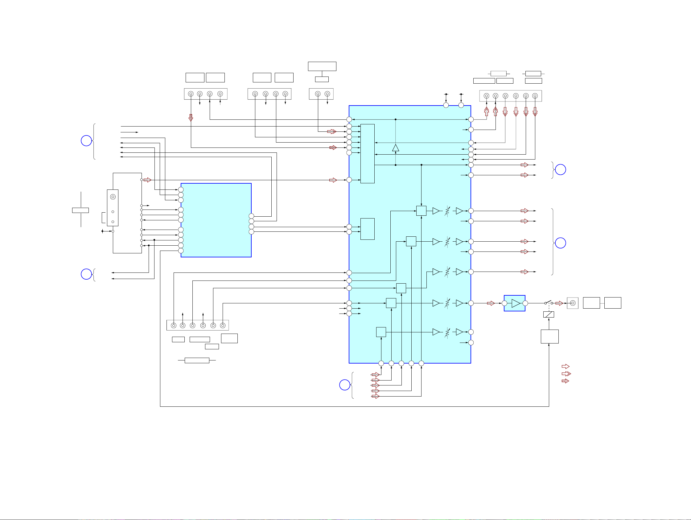
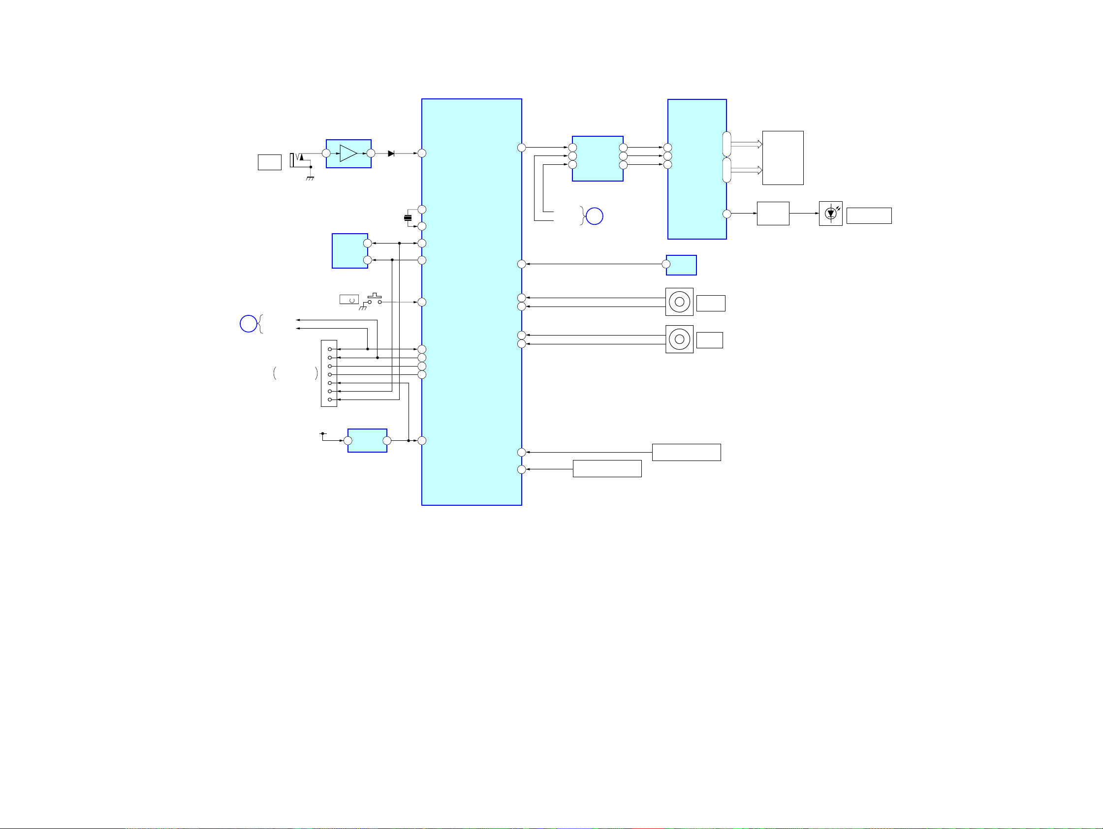
4-2. BLOCK DIAGRAM — TUNER/AUDIO SECTION —
SA-CD/CDINMD/TAPE
L
R
LR
R–CH
XM L
XM
SECTION
(Page 17)
ANTENNA
C
FM 75Ω
COAXIAL
TU+10V
XM R
XM REQ
XM DBPOWER
XM COMMAND
XM DACMS
XM RESET
FM/AM TUNER UNIT
AM
TN1
STEREO
TUNED
MUTING
CLOCK
L–CH
R–CH
DATA
R–CH
RDS DATA/XM COMMAND
53
RDS CLK/XM DPOWER
52
RDS SIG/XM REQ
R–CH
CE
DO
43
76
STEREO
75
TUNED
78
MUTE
S LATCH
74
73
DO
17
TUNER DATA/FL DATA
16
T.SERIAL CLK/FL CLK
SW RY
70
SYSTEM CONTROL
IC1101 (1/5)
OUT
VIDEO 3 IN/
PORTABLE AV IN
MD/TAPEINDVD AUDIO
LRLR
-3 -4 -1 -2
J403J402 J298(2/2) J404
R–CH
26
XM_RST
VOL DA
VOL CL
47
60
59
XM DACMS
R–CH
IN
R–CH
AUDIO
LR
-2 -3-3 -4 -1 -2
R–CH
DIR
FUNCTION SELECT
IC401
46
22
28
32
30
34
SEL
SW
36
38
L
SEL
MCU
60
I/F
59
SL
SEL
+7V–7V
68 66
AVCCAVEE
R–CH
R–CH
R–CH
R–CH
R–CH
R–CH
44
45
24
25
26
27
41
42
88
87
85
84
VIDEO 1
AUDIO OUT AUDIO INAUDIO IN
L
RL
-3 -4 -1 -2
VIDEO 2
RLR
-5 -6
L–CH
R–CH
L–CH
R–CH
SL–CH
SR–CH
A
E
DIGITAL
SECTION
(Page 15)
POWER
SECTION
(Page 19)
KEY/
DISPLAY
SECTION
(Page 18)
86
81
83
82
5 7
SUB WOOFER
AMP
IC402
R–CH
R–CH
10
13
12
17
11
R–CH
14
R–CH
SBL
SEL
54 56 51 52 49
SBL OUT
SW OUT
C OUT
B
SL OUT
L OUT
SW
SEL
SEL
C
R–CH
FL CLK
D
FL DATA
J401
R–CH
-5 -6 -3 -4 -1 -2
LR
FRONT
LR
SURROUND
MULTI CH IN
R–CH
CENTER
SUB
WOOFER
DIGITAL
SECTION
(Page 15)
C–CH
J309
RY560
RELAY
DRIVER
Q560
• Signal path
: TUNER (FM/AM)
: VIDEO (AUDIO)
: CD (ANALOG)
• R
–
ch is omitted due to
same as L
AUDIO
OUT
–
ch.
SUB
WOOFER
STR-K7000
1414
Page 15
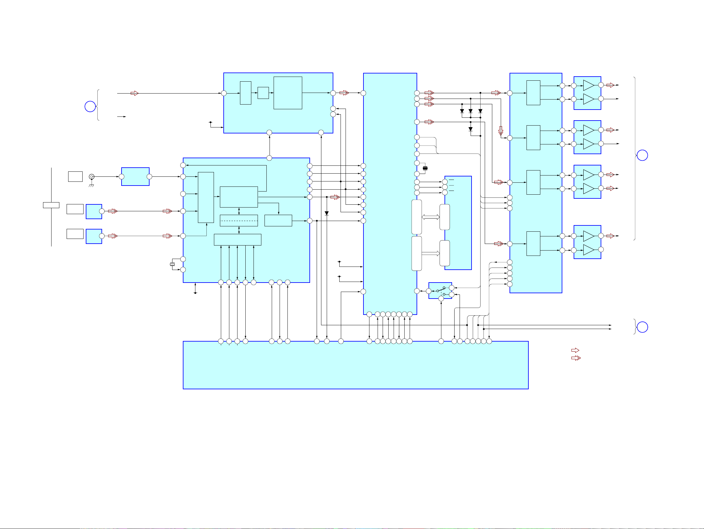
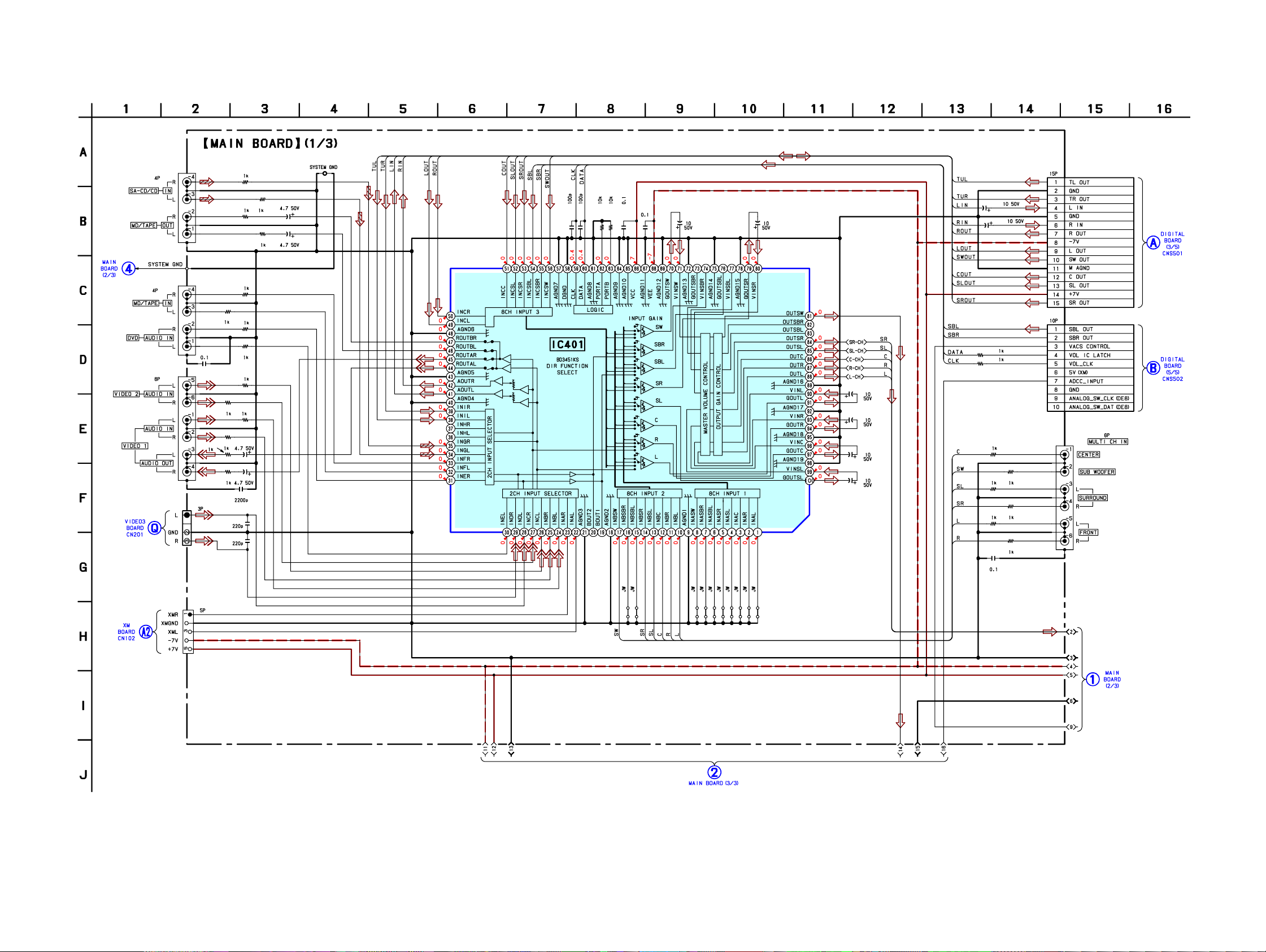
4-3. BLOCK DIAGRAM — DIGITAL SECTION —
STR-K7000
DIGITAL
TUNER/
AUDIO
SECTION
(Page 14)
DVD
IN
(COAXIAL)
VIDEO 1
IN
(OPTICAL)
VIDEO 2
IN
(OPTICAL)
A
J1301
IC1354
IC1351
OUT
OUT
L-IN
R-IN R-CH
1
1
IC1303
WAVE
SHAPER
ADC
IC1401
DOUT
15 18
LRCK
13
BCK
14
RST
6
24
13 22
14 29
15 28
16 30
D1301
34 59
+2.6V
VDDI
+3.3V
VDDE
DATAO
8
GP12
99
ERROR
SDI1 SD01
GP8
69
KFSI0
BCKI2
LRCKI2
SDI2
LRCKI1
15
BCKI1
17
EXLOCK
37
GP12
GP9
68
21
GP9
SYS CLK
16
20
XMCK
DETECTION
CKSEL1
94
CKSEL1
AUDIO
I/F
XSTATE
48
93100
XSTATE
AUDIO
CKOUT
BCK
LRCK
DATAO
ERROR
XMODE
XMODE
L IN
1
+5V-2
A.5V
DIGITAL AUDIO
I/F RECEIVER
IC1301
DOUT
2
23
X1301
12.288MHz
DIN2
5
SDIN
8
4
3
21
22
INPUT
DIN1
DIN0
XOUT
XIN
VDD
+3.3V
DATA
DEMODULATOR
Pa,Pb DETECTION LOCK
C bit DETECTION
MICROPROCESSOR
I/F
CLKCEDIDOBPSYNC
38 37 36 35 33 47 17
95 96 97 98
DIR DI
DIR CE
DIR_CLK
ADC
LPF
NC
DIR DO
HACN
HCS
HCS
HACN
SYSTEM
CONTROL
IC1101 (2/5)
DSP
IC1501
XRST
2 11336 35 33 3432
6 74 18 19 205
XRST
PM
PM
SD02
SD03
SD04
SCKOUT
LRCKO
BCKO
MCLK1
MCLK2
CSO
WEO
OEO
HDIN
HDOUT
HDIN
HDOUT
D0-15A0-15
BST
HCLK
HCLK
23
24
25
26
SCKOUT
14
LRCKO
19
BCKO
20
9
X1502
13.9MHz
12
44
45
43
98,80 - 77,75 - 72
108,107,105 -102,99,
85-82,66 - 64
112,110,109,97 - 92,
SWITCH
IC1503
56
5
6
92
D1503
SDRAM
IC1502
CS
6
17
WE
41
OE
D0-15A0-15
16-13,10 - 7
29 - 32,35 - 38,
1 - 5,18 - 21
24 - 27,42 - 44,
LRCKO
2
1
57
BST SEL
ADCC_INT
D1502D1504
BST
PCM1609 RST
PCM1609 ML
47
D1501
45
46
SCKOUT
38
LRCKO
41
BCKO
40
31
33
34
35
36
37
ADCC_INT ADCC_INT
15141312103
PCM1609 MDO
PCM1609 MC/XMDAC MC
PCM1609 MDI/XMDAC MDI
DATA3
DATA1
DATA2
SCKI
LRCK
BCK
DATA4
MDO
MDI
MC
ML
RST
8CH DAC
IC1452
DAC
DAC
DAC
DAC
VOUT5
VOUT6
VOUT1
VOUT2
VOUT3
VOUT4
VOUT7
VOUT8
AMP
IC1403
310
5
9
AMP
IC1405
514
3
13
AMP
IC1404
312
5
11
AMP
IC1406
516
3
20
• Signal path
: TUNER (FM/AM)
: VIDEO (AUDIO)
• R-ch is omitted due to
same as L-ch.
1
7
7
1
1
7
7
1
L OUT
R-CH
SL OUT
R-CH
C OUT
SW OUT
SBL OUT
XM DAC MC
XM DAC MDI
B
F
TUNER/
AUDIO
SECTION
(Page 14)
XM
SECTION
(Page 17)
STR-K7000
15 15
Page 16
STR-K7000
4-4. BLOCK DIAGRAM — VIDEO SECTION —
COMPONENT VIDEO SELECT
IC304
SW1 SW2
COMP SW1 COMP SW2
2 4
(ASSIGNABLE)
COMPONENT
VIDEO
(ASSIGNABLE)
VIDEO 2
IN
DVD
IN
VIDEO 1
VIDEO 2
DVD
P
P
P
P
B/CB/
R/CR/
B/CB/
R/CR/
-1
VIDEO
IN
-2
VIDEO
IN
-1
VIDEO
IN
J301 (1/2)
Y
B-Y
R-Y
Y
B-Y
R-Y
J201 (1/2)
J200 (1/2)
CH1 IN2
-4
-5
-6
-1
-2
-3
3
CH1 IN3
5
CH2 IN2
9
CH2 IN3
11
CH3 IN2
14
CH3 IN3
12
VIDEO
SELECTOR
IC203
V1
13
V2
5
DVD
3
6dB AMP
6dB AMP
6dB AMP
75Ω
DRIVER
75Ω
DRIVER
75Ω
DRIVER
CHI OUT
CH2 OUT
CH3 OUT
V+1,+2
22
20
18
V-1,-2
6dB AMP
6dB AMP
+5V-3
-5V-3
J301 (2/2)
75Ω
DRIVER
75Ω
DRIVER
Y
-7
+5V-3
-5V-3
COMPONENT
VIDEO
IC807
1 3
REG
IC804
3 2
REG
+5V
-5V
+15V
-15V
J200 (2/2)
J201 (2/2)
-3
VIDEO
OUT
-2
VIDEO
OUT
VIDEO 1
MONITOR
88
D595 OE
89
D595 LAT
87
D595 CLK
D595 DATA
86
SYSTEM
CONTROL
IC1101 (3/5)
P
B/CB/
-8
R/CR/
P
-9
V1.OUT
M.OUT
MONITOR
B-Y
OUT
R-Y
VCC
+5V-3
15
1
STR-K7000
VIDEO 3 IN/
PORTABLE AV IN
• Signal path
: VIDEO
HDMI
-1
VIDEO
DVD IN
(ASSIGNABLE)
VIDEO 2 IN
(ASSIGNABLE)
MONITOR OUT
J298 (1/2)
CN5001
1
3
4
6
7
9
10
12
15
16
19
13
18
CN5002
1
3
4
6
7
9
10
12
15
16
19
13
18
CN5003
1
3
4
6
7
9
10
12
15
16
19
13
18
DATA2+
DATA2–
DATA1+
DATA1–
DATA0+
DATA0–
CLOCK+
CLOCK–
SCL(5V)
SDA(5V)
HOT PLUG DET
CEC
+5V POWER
DATA2+
DATA2–
DATA1+
DATA1–
DATA0+
DATA0–
CLOCK+
CLOCK–
SCL(5V)
SDA(5V)
HOT PLUG DET
CEC
+5V POWER
DATA2+
DATA2–
DATA1+
DATA1–
DATA0+
DATA0–
CLOCK+
CLOCK–
SCL(5V)
SDA(5V)
HOT PLUG DET
CEC
+5V POWER
IC1602
14
HDMI
CONTROL
CTL(HDMI)
7
PRE(HDMI)
6
OEB(HDMI)
5
SI(HDMI)
4
+3.3V
REG
IC1601
7
6
5
VIDEO
4
CONTROL
3
2
13 13
12 12
11 11
SIN SOUT
14 9
1
+5.8V
4 2
REG
IC5006
DATA
+7V
LAT
CLK
OE
V3
9
NC
7
SW2
SW3
SW4
SW4
IC5001
SW1
SW1
D203,204
10 6 14 2
4
SW2
SW3
HDMI RECEIVER/TRANSCEIVER
77
A24
B24
76
A23
74
73
B23
71
A22
B22
70
68
A21
67
B21
SCL2
64
63
SDA2
62
HPD2
15
A14
B14
14
A13
12
11
B13
9
A12
B12
8
6
A11
5
B11
3
SCL1
2
SDA1
80
HPD1
25
Y4
Z4
26
Y3
28
29
Z3
31
Y2
Z2
32
34
Y1
35
Z1
38
SCL SINK
39
SDA SINK
40
HPD SINK
SW5
OR
42
OEB
21
S1
LEVEL SHIFT
IC5004
1
5
3
7
VEE
-5V-3
6
1
3
ANALOG SWITCH
IC5005
4
4 5
1
POWER
CONTROL
IC5002
HDMI+3.3V
SW1
SW2
SW3
SW4
COMP SW1
COMP SW2
3 1
IC5003
1616
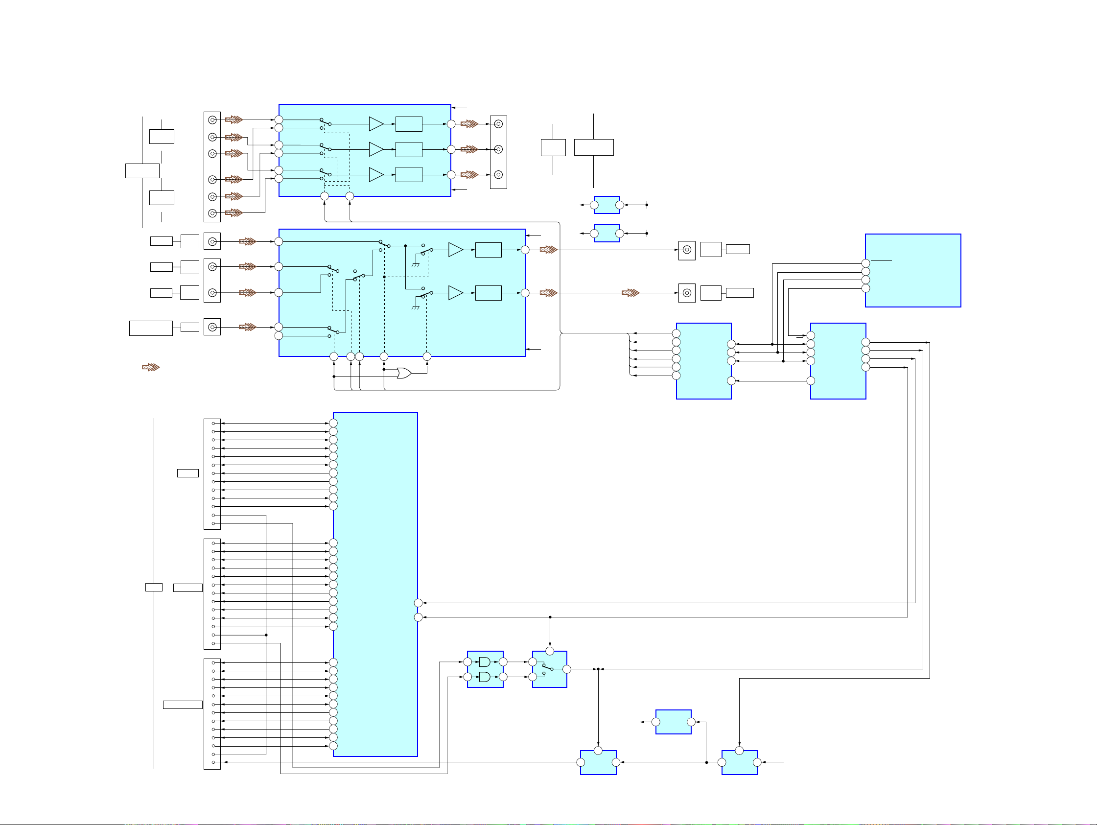
Page 17
4-5. BLOCK DIAGRAM — XM SECTION —
XM DIGITAL
TRANSCEIVER
J101
XM
IC102
18 COMRXP
19 COMRXT
+D
2
–D
3
23 COMTXP
22 COMTXM
SCTXOUT
SCRXIN
COMMSEL
IRQ
3
5
7
9
XM64FS
XMDATA
XMFS
XM256FS
STR-K7000
3
12
11
BUFFER
2
IC103
6
7
5
4
8
17
9
18
XM MIXMI
XM MIXMO
KEY/DISPLAY
G
SECTION
(Page 18)
XMCOMMAND
XMREQ
X101
45.158MHz
26 OSCOUT
28 OSCIN
I2SSCLK
I2SDATA
I2SLRCLK
I2SOCLK
RESET
13
MD
14
IC105
MC
ML
VOUTL
VOUTR
XM+5.3V
3 1
15
7
8
XM+5V
IC101
XM+3.3V
REG
BCK
39
37
41
43
11
RESET
Q101,104
1
2
3
16
XM+3.3V
DATA
LRCK
SCK
D/A CONVERTER
XM DACMDI
XM DACMC
1
4 2
XM5.3V REG
IC106
IC107
XM+5V
3 1
REG
DIGITAL
F
SECTION
6 7
2
XM AMP
IC104
(Page 15)
1
RECT
D104
F40
XMDACMS
XML
XMR
XM RESET
DBPOWER
AC1
AC2
TUNER/AUDIO
C
SECTION
(Page 14)
STR-K7000
17 17
Page 18
STR-K7000
4-6. BLOCK DIAGRAM — KEY/DISPLAY SECTION —
XM
SECTION
(Page 17)
SIRCS
FL DISPLAY DRIVER
IC100
STB
9
DIN
7
CLK
8
OUT
1
1
3
1
3
SEG1
I
SEG16
GRID12
I
GRID1
SW1
REMOTE
CONTROL
RECEIVER
IC102
RV101
INPUT
SELECTOR
RV102
MASTER
VOLUME
14
I
29
31
I
42
1
FL101
VACUUM
FLUORESCENT
DISPLAY
LED
DRIVER
Q110
D105
MULTI CHANNEL
DECODING
SYSTEM
CONTROL
MIC AMP
IC2000
J2000
AUTO
CAL MIC
EEPROM
IC1131
SDA
SCL
S100
I
/
I
XM MIXMO
G
XM MIXMI
FLASH
PROGRAMMING
CNP504
1
2
7
6
5
8
9
FLASH1
FLASH2
MD2
MD0
RESET
SCL
SDA
D2014
15
X1101
24MHz
5
6
38
83
82
29
30
56
28
27
51
49
IC1101 (4/5)
ADCC
X1
X0
SDA
SCL
POWER KEY
FLASH1/XM_TX
FLASH2/XM_RX
MD2
MD0
FL LAT
SIRCS
ENC A
ENC B
VOL ENC A
VOL ENC B
FL CLK
FL DATA
9
BUFFER
4
IC101
2
8
6
3
TUNER/
AUDIO
D
SECTION
9
(Page 14)
54
31
32
65
64
+3.3V
(STBY)
IC1111
RESET
12
77
RSTX
A/D1
A/D2
39
40
SW NETWORK
S101–107,124
SW NETWORK
S108–111,115
STR-K7000
1818
Page 19
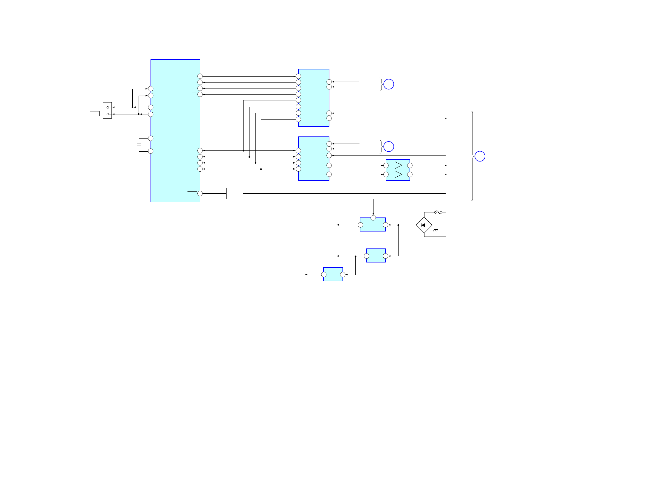
4-7. BLOCK DIAGRAM — POWER SECTION —
PRE DRIVER
IC701
IN 2
PRE
PRE
PRE
D1107
DRIVE
PRE DRIVER
IC601
DRIVE
PRE DRIVER
IC501
DRIVE
Q722,723,725,793,795
D1111
FRONT-RY
REAR-RY
CENTER RY
HP DETECT
PROTECTOR
D721,722,732
HP-RY
SB-RY
TUNER/
AUDIO
SECTION
(Page 14)
E
L-CH
R-CH
R-CH
SL-CH
SR-CH R-CH
C-CH
PROTECTOR
FRONT RY
HP DETECT
SYSTEM
CONTROL
IC1101 (5/5)
BRIDGEABLE RY
P0WER RY
HP_RY
REAR_RY
C/SB RY
SP_B_RY
STOP
8
8
8
61
62
66
69
68
55
67
72
58
48
IN 2
IN2
D1110
DRIVE
DRIVE
DRIVE
D1108
+VOUT2
-VOUT2
-B-1 +B-1
+VOUT2
-VOUT2
-B-1 +B-1
+VOUT2
-VOUT2
-B-1 +B-1
12
11
12
11
12
11
DETECT AMP
-B-1
IC691
OVERLOAD
+B-1
POWER AMP
Q701-704
POWER AMP
Q651-654
POWER AMP
Q501-504
B- SWITCH
Q691,692
72
B+ SWITCH
Q693-695
STR-K7000
J791
PHONES
R-CH
TM602
TM601
TM502
AC1
AC2
L
R
L
R
L
R
TRANSFORMER
R810
R811
R910
TRANSFORMER
D915
FRONT B
FRONT A
SURROUND
CENTER
T901
POWER
T902
POWER
SPEAKERS
IMPEDANCE
USE 6-16Ω
• Signal path
: TUNER (FM/AM)
• R-ch is omitted due to
same as L-ch.
F901
AC IN~
RELAY
FRONT RY
REAR-RY
CENTER RY
13
31
13
13
DRIVER
Q790
RELAY
DRIVER
Q800
RELAY
DRIVER
Q710
HP DETECT
+15V
-15V
RELAY
DRIVER
Q610
RELAY
DRIVER
Q550
RECT
D802
RY791
RY600
RELAY
DRIVER
Q809
RY601
RY501
RY701
RELAY
DRIVER
Q901
R-CH
R-CH
R-CH
RECT
D920-923
RECT
D805-808
D910-913
AC IN
DETECT
Q921
RECT
F1
F2
RELAY
SWITCH
RY801
RY901
D914
CURRENT
DETECT
Q705,706
R-CH
R-CH
CURRENT
DETECT
Q655,656
R-CH
+B
-B
-20V
TU+10V
+7V
-7V
+5V-2
+5V-1
+2.6V
+3.3V
+3.3V
(STBY)
IC1904
+3.3V
R-CH R-CH
CURRENT
DETECT
Q505,506
-20V REG
Q801
13
REG
5
+3.3V/+2.6V
2
OVERLOAD
D740,Q740
OVERLOAD
D640,Q640
OVERLOAD
D540,Q540
IC1001
+5V
REG
IC1901
REG
DETECT
R-CH
DETECT
DETECT
13
HP-RY
SB-RY
IC1902
+9V
REG
IC801
+7V
REG
-7V
REG
IC802
+5V
REG
4
IC1031
STR-K7000
19 19
Page 20
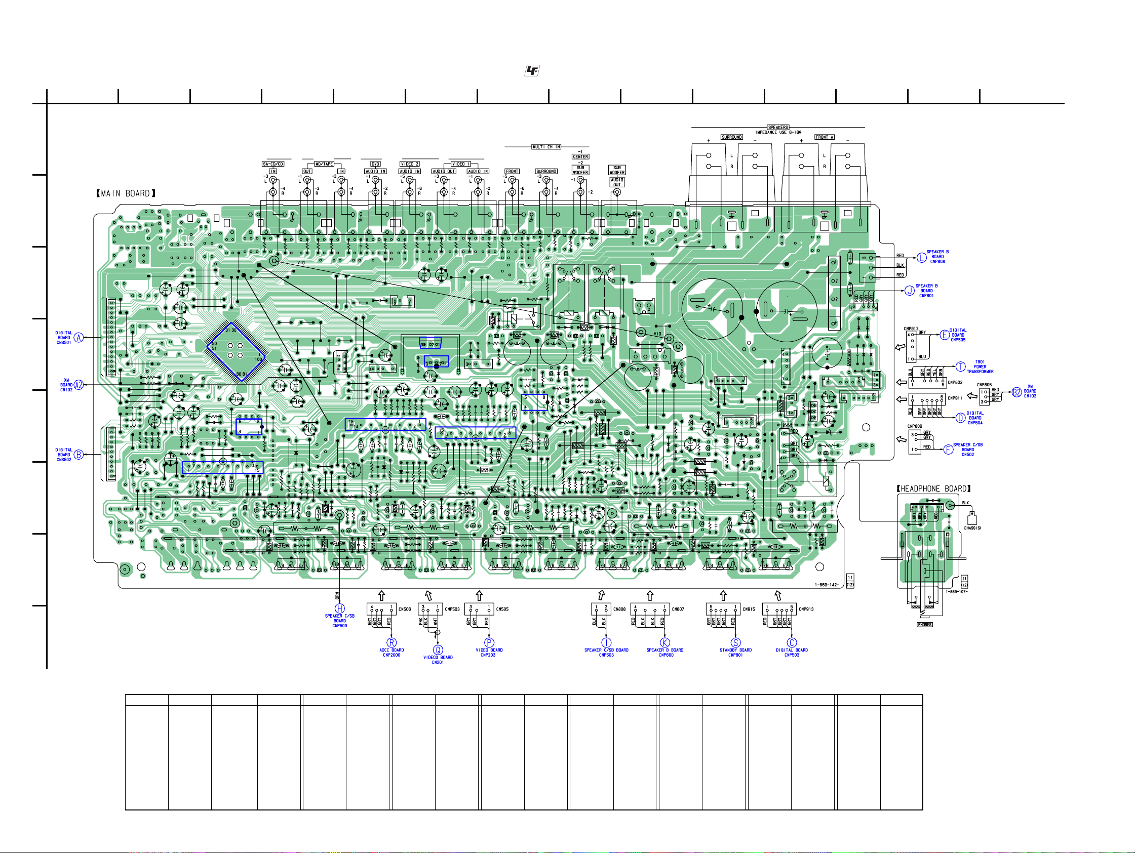
STR-K7000
4-8. PRINTED WIRING BOARDS — MAIN SECTION — • Refer to page 12 for Circuit Boards Location. : Uses unleaded solder.
A
B
C
D
E
F
G
(Page 25)
(Page 37)
(Page 25)
1
1
0
5
P
N
C
234567891011 12 13 14
TM601
J401
3
2
3
W
J
0
0
5
P
N
C
TP801
J402
8
2
2
5
42
4
W
R
0
4
5
Q
WP100
JW435
3
4
4
JW
4
2
4
W
J
C510
J
JW470
C482
JW469
C493
C481
8
1
3
7
JW
1
3
W
J
0
8
4
R
9
8
3
1
5
4
R
JW
C540
0
4
5
D
4
C517
1
5
R
3
1
4
R474
C499
JW503
5
0
5
R
JW
5
1
4
6
3
4
JW
JW
IC401
C485
0
2
3
W
J
IC402
2
7
0
0
5
5
C
R
JW505
IC501
6
0
5
0
C
2
4
W
J
1
5
4
3
0
0
4
5
5
C
C
W
J
1
0
5
Q
WP02
JW440
C488
1
0
5
C
C495
C702
0
5
4
JW
C762
JW438
JW439
9
0
4
C
JW410
JW409
C464
2
7
4
C
3
7
1
4
9
0
9
R
5
4
R
R
JW474
R741
2
0
5
JW
JW429
3
0
5
R
JW437
9
5
4
C469
C468
R428
R429
C
1
1
4
W
JW456
4
4
8
R
8
0
5
JW
R475
R476
JW324
2
4
8
C
2
3
4
W
J
J
1
2
3
JW
0
1
3
4
4
4
8
8
8
R
D
R
C741
1
0
5
JW
8
5
4
5
5
JW
4
W
J
JW454
JW425
JW451
0
4
8
JW
C503
4
0
5
W
J
6
0
5
JW
2
1
4
JW
3
5
4
W
J
2
5
4
W
J
9
0
5
4
4
R
R
C483
0
1
2
2
5
5
C
C
3
1
5
C
0
2
0
9
5
4
C
C
JW
C484
JW444
C471
0
1
9
2
5
2
2
5
3
W
D
J
JW
5
5
5
R
7
5
5
R
Q503
JW708
9
2
5
C
7
5
6
3
9
2
74
5
7
2
5
5
R
5
5
R
R
R
R
1
6
0
4
4
4
6
5
5
5
0
C
R
R
5
Q
R516
5
1
R513
5
R
R510
R511
Q502
J403 J404
4
9
5
0
4
4
R
R
0
3
4
JW
6
6
4
W
J
C523
2
2
5
C
8
1
5
C
2
1
5
C
H
117
1
70
W
J
6
7
3
3
6
6
2
W
4
J
7
JW
C
5
0
5
WP03
D
7
1
1
1
5
5
C
R
C516
Q504
2
70
W
J
Q505
9
1
4
JW
R740
5
3
5
04
0
4
4
4
R
R
C
C453
C463
JWH118
7
6
8
4
6
4
JW
JW
C807
JW311
4
JW312
0
5
N
C
JW313
CN506
JW314
C703
JW315
JW316
3
0
7
R
IC701
4
0
05
7
7
C
C
C732
0
4
7
D
1
2
5
R
9
9
9
2
2
2
7
7
7
D
R
C
3
0
7
JW
5
6
4
74
7
R
R
8
4
7
2
4
R
2
52
01
5
7
R
R
C710
Q
0
4
2
1
5
7
R
C519
R
J309
0
40
C
5
R436
R470
5
61
JW
Q652
5
33
4
4
4
R
C
9
6
4
R
R618
L601
4
11
H
JW
9
8
6
R
4
1
6
W
J
4
0
6
R
1
2
8
8
5
5
W
W
J
J
78
5
JW
3
7
6
R
5
8
0
5
4
4
6
6
6
Q
R
R
R666
JW509
5
6
6
R
34
3
4
4
R
R
1
0
6
Y
R
D610
R634
Q710
Q610
1
1
3
3
7
6
20
R
R
8
JW
4
3
2
9
9
9
6
6
6
D693
Q
Q
D
R700
R697
R705
2
Q695
9
1
6
6
9
9
Q
6
6
0
D
R
9
R706
6
D
R693
R694
04
6
C
2
1
6
JW
5
7
7
R
7
2
7
4
6
6
R
C
9
6
6
C
Q654 Q753
8
9
6
R
1
1
1
6
9
6
JW
R
5
3
0
5
1
1
7
6
6
W
JW
J
JW
R758
C750
0
7
3
0
2
5
5
7
5
5
7
7
7
7
7
R
R
R
C
D
C640
4
5
2
0
7
6
7
4
6
6
6
6
R
D
R
D
C760
Q656
1
9
0
7
7
6
66
6
R
R
C
D710
JWH116
3
62
R
JW569
4
6
7
R
8
1
8
JW
32
7
R
R692
TP800
JW774
JWH122
JW771
1
0
7
Y
CN808
R
70
7
JW
JW800
WP04
L701
R761
R760
Q752
0
2
7
W
J
R655
R656
JW767
CN807
2
72
JW
7
1
8
W
J
WP102
WP101
8
6
18
7
7
R
R
1
5
7
8
2
1
5
W
7
7
J
JW
JW
23
6
7
2
3
2
7
7
R
JW
D
6
7
1
1
7
7
W
W
J
J
7
0
5
8
6
6
R
Q
4
8
5
5
JW
1
5
6
7
7
Q
C
R766
JW620
5
6
7
C767
R
Q754
4
3
7
R
4
1
7
Q691
JW
R699
7
6
5
7
83
W
J
5
6
JW
5
5
7
7
R
R
Q750
R767
JW819
Q751
5
4
4
W
J
JW816
R763
C766
C804
1
5
7
L
8
0
1
H
JW
4
5
0
7
8
W
7
J
R
C722
1
2
7
D
R794
R792
C680
0
8
6
D
5
8
6
72
7
77
7
D
R
R
1
7
7
R
CN915
13
8
1
9
W
5
2
J
1
7
71
7
W
JW
J
JW
3
5
7
5
C791
JW
79
Q
59
5
JW
R614
CNP913
1
25
1
7
3
7
Q
1
37
W
22
7
7
J
7
W
R
Q
J
5
3
7
R
5
2
7
6
C681
1
R
6
R
6
1
9
5
0
2
6
7
7
6
7
7
Q
C
R
C
R610
R611
Q603 Q604
C721
8
3
7
W
J
JW568
C610
Q601
3
1
6
R
Q602
3
6
7
JW
2
3
7
D
1
8
6
R
15
6
R
2
1
7
W
J
3
9
7
Q
0
8
6
R
JW601
C803
7
6
80
80
W
JW
J
3
9
7
R
4
5
0
0
8
8
R803
JW
JW
3
2
2
9
7
7
Q
N
C
1
2
1
1
8
8
W
JW
J
2
3
80
80
W
W
J
J
1
1
6
C
C620
JW783
9
0
0
2
8
1
1
7
9
JW
P
JW
N
C
8
80
JW810
W
J
6
4
80
80
P
R
N
C
C809
C822
RY791
4
2
5
6
2
2
0
0
6
6
6
6
R
R
D
Q
R616
2
0
0
2
6
6
R
JW
1
0
8
Q
Q790
5
0
6
Q
D804
D791
C832
C802
R791
5
0
8
C
1
0
8
2
80
D
CNP802
D801
R806
C801
P
N
C
06
8
C
CN507
8
7
0
0
8
8
D
D
6
1
5
0
3
0
0
8
8
8
1
C
9
D
D
R
C830
CNP805
CNP911
(Page 31)
(Page 31)
(Page 25)
(Page 31)
C791
9
61
C
1
62
R
CNP791
JW791
0
79
T
B
TP701
90
7
C
8
7
5
0
4
R
4
1
4
JW
CNP503
C701
7
2
1
0
0
0
7
7
7
C
R
R
6
4
6
5
0
0
7
7
7
C
R
C
9
4
9
7
3
D
7
R
0
4
7
Q
R717
C717
Q703
4
7
0
4
5
4
4
4
C
R
R
8
8
5
0
4
4
C
C
IC801
IC802
6
9
8
D
C808
C751
C753
7
1
2
3
5
5
5
5
7
7
7
7
C
R
R
R
C655
4
4
7
R
4
4
5
5
5
5
7
7
7
R
C
C
9
4
7
6
9
C
2
4
6
7
R
9
JW
5
7
C733
R
JWB03
5
2
C740
7
R
1
6
1
0
7
7
C
Q
R716
R713
5
1
7
R710
R
R711
Q702
6
8
0
5
5
4
4
4
R
R
R
JW461
3
6
4
W
J
0
1
8
C
CN505
C653
2
3
1
5
5
5
6
6
6
R
R
R
IC601
6
5
0
7
D
C716
Q704
6
0
3
7
7
7
0
W
JW
7
J
0
8
3
2
6
6
JW
W
JW
J
R723
0
9
2
1
7
7
C
R
1
4
72
Q705
2
R
7
R
JW507
JWB02
JWB01
4
4
7
C
1
4
5
6
R
C660
1
0
6
R
C666
Q653
R468
0
6
5
D
2
3
5
R
0
4
6
Q
2
3
3
4
4
R
R
JW416
RY560
R668
L651
R695
3
0
C691
6
C
R690
IC691
5
3
6
0
0
0
6
6
6
C
R
C
3
4
7
C
3
4
4
5
7
6
R
C
5
7
6
6
8
7
3
R
6
6
R
R
1
6
6
C
R663
R660
R661
6
0
4
R
4
5
6
6
4
4
W
J
JW
2
0
8
R
Q560
R533
1
1
8
C
1
1
65
60
C
C
2
7
7
0
5
0
6
6
6
R
C
C
5
6
3
5
7
6
C
JW
R733
JWH112
R667
2
2
1
7
5
R
6
Q
4
6
6
R
(Page 42)
(Page 37)
(Page 25)
H
STR-K7000
(Page 31)
(Page 39)
(Page 33)
• Semiconductor Location
Ref. No. Location Ref. No. Location Ref. No. Location Ref. No. Location
D505 F-4
D529 E-4
D540 F-3
D560 D-7
D605 F-11
D610 D-8
D640 F-8
D665 F-8
D680 F-9
D690 E-8
D691 E-8
D692 D-8
D693 D-8
D705 F-6
D710 D-8
D721 E-9
D722 E-9
D729 F-5
D732 F-10
D740 F-5
D749 F-5
D750 F-8
D765 F-9
D791 E-11
D801 E-11
D802 C-11
D804 E-11
D805 D-12
D806 D-12
D807 D-12
D808 D-12
D841 E-2
D896 D-6
IC401 D-3
IC402 E-3
IC501 F-3
IC601 E-6
IC691 E-7
IC701 E-5
IC801 D-6
IC802 D-6
Q501 F-3
Q502 G-4
(Page 33) (Page 31) (Page 31)
Ref. No. Location
Q503 G-4
Q504 G-5
Q505 F-5
Q506 F-4
Q540 F-3
Q560 D-7
Q601 G-10
Q602 G-10
Q603 G-10
Q604 G-11
Q605 F-11
Ref. No. Location Ref. No. Location
Q606 F-11
Q610 D-8
Q640 F-7
Q651 F-7
Q652 G-7
Q653 G-7
Q654 G-8
Q655 F-7
Q656 F-8
Q680 F-9
Q691 E-9
Q692 E-8
Q693 D-8
Q694 D-8
Q695 E-8
Q701 F-5
Q702 G-6
Q703 G-5
Q704 G-6
Q705 F-6
Q706 F-6
Q710 D-8
2020
(Page 42)
(Page 25)
Ref. No. Location
Q722 E-10
Q723 E-10
Q725 E-10
Q740 F-5
Q750 F-8
Q751 F-9
Q752 G-9
Q753 G-8
Q754 G-9
Q755 F-9
Q756 F-10
J791
Ref. No. Location
Q790 E-11
Q793 F-10
Q795 E-10
Q801 E-11
Page 21
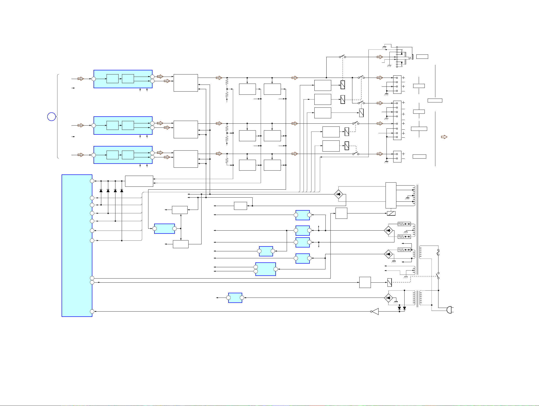
4-9. SCHEMATIC DIAGRAM — MAIN SECTION (1/3) —
STR-K7000
(Page 22)
(Page 34)
J402
J403
J404
C403
CNP503
R408
R404
R457 R406
R456
R458
C458
C444
C463
C453
R452
R459
R454
R455
R405
R407
C408
R402
R409
C459
C409
WP100
IC401
C469
C468
R475
R476
C488
C464
CNP501
C702
C485C495
C762
(Page 28)
CNP500
R429
R428
C484
C481
C492
C493
J401
R436
R435R434
R433R432
R431
C445
(Page 30)
STR-K7000
(Page 38)
CN504
C482
C483
C523
C522
(Page 23)
21 21
C521
C520
C518
C513
C512
C500
(Page 22)
Page 22
STR-K7000
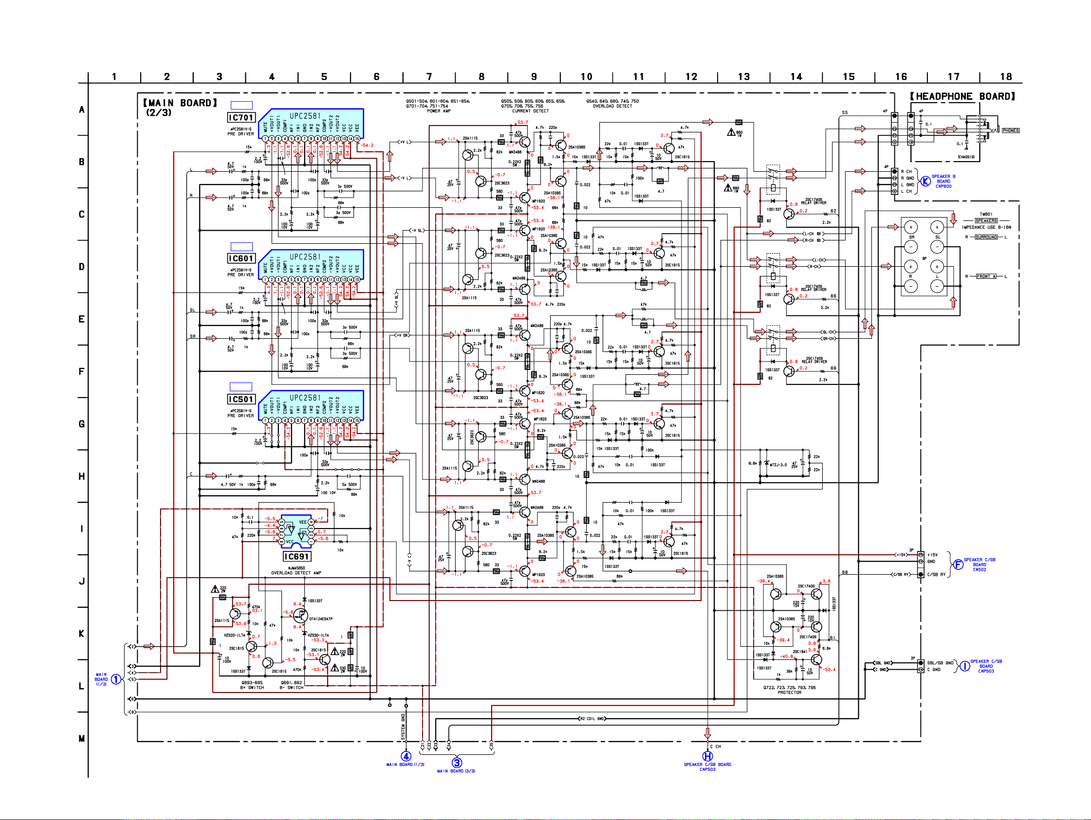
4-10. SCHEMATIC DIAGRAM — MAIN SECTION (2/3) — • Refer to page 44 for IC Block Diagrams.
(Page 21)
R732
R706
Q695
C701
C751
C651
C601
C501
C732
IC B/D
IC701
R701
R751
IC B/D
IC601
R743
R651
C607
IC B/D
IC501
R741
R501
R695
R696
D693
Q694
D692
C707
C757
C657
R601
R744
C507
C691
R690
C743
R705
R700
C744
C741
JW504
R702
R752
R652
R602
C755
R753
C753 C703
C605
R603
JW502
JW501
R502
R697
Q693
R689
IC691
R698
R699
C756
C606
C506
C653C603
C706
R703
R653
C656
D691
Q692
D690
Q691
C705
C704
R704
C754
R754
C655
C505
R503
C503
C654
R654
C604
R604
JW503 JW505
C504
R505
R693
R694
R733
R691
R692
C733
WP101
WP102
C510
C710
C660
C610
C760
Q751
R510
Q501
Q651
Q701
Q601
Q752
R710
R660
R610
Q602
R511
Q502
R513
R514
R515
R714
R711
R713
R715
R665
R663
R661
R614
R611
R613
R615
Q702
Q652
R664
R765
R763
R761R760
R764
C516
Q703
R716
R666
C666
R616
R766
C766
C517
R516
C717
C716
C669
Q653
C621
C620
C767
R719 C720
R722
R721
Q706
Q704
R725
R638
Q654
Q655
R671
Q656
R669 C670
Q603
R621
Q604
Q754
R771
R769 C770
Q753
Q503
Q505
R521
Q504
R672
Q756
Q606
R622
R772
CNP806
CN808
CNP791
TM601
C790
(Page 32)
J791
C791
TP701
(Page 32)
CN792
R745
D740
C742
C711
R717
R667
C661
R674 D665
C611
R617
Q605
R624
D605
R625
Q755
C761
R522
R524
Q506
D705R724
R673
R640
R778 D765
R773
R517
C511
R750
R740
R723
R681
R758
R525
R680
R546
D505
R540
C642
R648
R573
C681
C752
R757
C729R729
R657
C541
R768
R557
WP03
R677
D640
R618
L751
D750
R739
D680
C680
D729
R668
R623
C640
L651
L601
C750
R759
D540
Q705
R620C619
R775
R767
R520C519
D749C749R749
C740
L701
R718
C540
R746
Q740R747R748
R675
R676
Q640
R655
R656
Q680
R755
R756
Q750
D529R539C529R529
R555
R556
Q540
R794
R792
R840 C842
D722
D721
R780
R793
R734
RY791
RY701
D710
RY601
D610
R634
D791
Q795
D841
R736
Q725
R737
C791
Q722
Q793
Q723
C722
C721
CN807
Q790
R791
Q710
R731
Q610
R631
R843
R844
D732
R735
(Page 32)
STR-K7000
(Page 21)
(Page 23)
(Page 32)
2222
Page 23

4-11. SCHEMATIC DIAGRAM — MAIN SECTION (3/3) —
STR-K7000
(Page 21) (Page 22)
(Page 34)
(Page 32)
(Page 39)
J309
C400
CN506
CN505
CN507
CNP911
R470
R469
R802
RY560
D560
R468
Q560
C803
C804
D802
C805
C806
CNP801
(Page 32)
CNP805
(Page 38)
CNP802
IC402
R532R533
R499
IC801
C807
C808
D896
C811
C810
R474
R473
C471
C499
C822
D804
R806
C472R480
C832
Q801
C801
C802
D808
D805 C831
C830D806
D807
R803
R804
C809
D801
R910
(Page 43)
IC802
(Page 29)
(Page 29)
(Page 29)
CN915
CNP913
(Page 43)
CNP912
STR-K7000
23 23
Page 24

STR-K7000
4-12. PRINTED WIRING BOARD — DIGITAL SECTION (1/2) — • Refer to page 12 for Circuit Boards Location. : Uses unleaded solder.
• Semiconductor
Location (Side A)
Ref. No. Location
D1001 D-5
D1301 F-10
D1302 E-11
IC1101 G-5
IC1111 F-5
IC1131 H-6
IC1301 E-10
IC1303 F-11
IC1401 H-11
IC1403 H-10
IC1404 H-9
IC1405 H-8
IC1406 H-7
IC1452 G-10
IC1501 F-9
IC1502 E-9
IC1503 G-8
IC1601 F-7
IC1602 E-7
R1354
C1362
JR1303
R1351
C1304
FB1306
IC1303
R1358
R1362
R1301
JR1302
C1302
D1302
R1359
C1360
C1357
R1357
R1356
C1361
C1303
C1405
IC1401
C1315
C1301
R1318
JR1005
R1303
R1304
FB1453
C1408
R1402
R1321
JR1511
R1305
R1401
FB1405
IC1301
R1306
R1360
R1319
JR1020
JR1008
R1407
R1403
R1316
R1312
R1307
R1308
D1301
C1522
R1556
IC1452
R1460
FB1452
R1310
R1309
X1502
FB1503
R1502
C1483
C1542
C1002
R1315
X1301
FB1305
C1521
R1505
R1506
R1461
R1492
R1483
R1484
R1486
R1010
R1313
R1311
R1513
R1507
R1011
R1512
R1515
R1523
R1503
R1504
IC1403
C1487
R1501
C1511
C1509
R1444
C1441
R1445
C1251
R1012
RB1506
R1508
R1491
C1253
R1013
R1514
R1014
IC1502
RB1501
R1471
R1470
C1472
R1446
R1476
R1015
RB1502
IC1501
R1472
R1473
R1016
RB1504
R1509
R1475
R1434
C1432
IC1404
C1566
R1017
R1435
R1436
C1569
R1555
RB1503
R1574
R1420
R1495
R1464
C1567
R1426
C1913
R1557
RB1500
RB1507
RB1508
R1573
R1570
R1571
R1572
C1502
IC1503
R1510
R1421
R1493
R1463
C1462
R1541
R1511
IC1405
R1137
R1049
R1144
R1161
R1155
R1424
R1067
R1066
R1065
R1150
R1134
R1142
R1143
C1422
R1425
R1162
R1149
R1494
R1455
C1568
R1466
R1063
R1061
R1135
R1160
R1490
C1451
C1557
R1062
R1068
R1041
R1120
R1044
C1255
R1454
R1416
JR1202
R1042
R1153
R1076
IC1406
IC1602
IC1601
R1136
R1151
R1805
R1140
C1254
R1414
R1806
R1130
C2217
R1121
R1154
R1152
C1411
R1185
C1105
R1803
C1104
R1095
R1116
C1102
R1156
IC1131
R1094
R1188
R1113
R1119
R1157
R1084
D1001
R1115
R1111
R1125
IC1101
C1142
C1118
R1194
R1164
R1081
R1110
R1126
X1101
C1620
C1119
R1109
R1524
R1127
R1122
R1123
R1129
R1083
R1124
R1635
R1107
C1137
R1189
C1605
C1604
R1636
R1201
R1112
R1035
R1114
IC1111
C1107
C1129
R1108
R1128
C1130
C1131
R1191
R1804
R1802
C1122
C1123
R1078
R1106
C1132
R1187
R1801
R1077
R1807
R1192
FB1308
R1117
R1118
R1103
R1097
R1182
R1172
R1171
R1179
R1180
R1088
R1073
R1072
R1183
R1184
R1181
2345678910111213
1
A
B
C
D
E
F
G
H
I
STR-K7000
2424
Page 25

4-13. PRINTED WIRING BOARD — DIGITAL SECTION (2/2) — • Refer to page 12 for Circuit Boards Location. : Uses unleaded solder.
STR-K7000
A
B
C
D
E
F
G
H
I
1
(Page 20)
2345678910111213
D1501
D1003
C1450
C1494
C1005
IC1001
(Page 33)
CNS509
C1314
C1308
C1306
C1457
R1474
C1454
C1404
C1409
C1406
C1305
R1302
C1359
C1403
C1358
C1355
C1401
C1402
C1407
JR1207
C1354
C1351
IC1354
IC1351
J1301
R1355
• Semiconductor
Location (Side B)
Ref. No. Location
D1003 G-10
D1004 G-10
D1107 F-5
D1108 F-5
D1110 F-5
D1111 F-5
D1501 F-10
D1502 F-10
D1503 F-10
D1504 G-10
(Page 20)
(Page 40)
IC1031
CNS504
C1031
C1905
C1908
C1032
CNP504
CNS505
(Page 42)
IC1901
C1100
R1105
C1171
R1186
C1172
C1906
C1022
C1140
C1108
C1021
R1039
D1111
C1138
R1190
IC1904
CNP503
D1107
D1110
C1299
FB1101
D1108
R1163
C1120
C1124
CNP505
C1103
C1121
R1082
FB1502
C1149
R1096
C1139
R1159
JR1104
CNS502
CNS503
C2216
C2218
C1602
C1145
C1146
(Page 20)
FB2034
C1601
C1144
C1495
C1413
C1478
(Page 37)
FB1501
JR1015
C1518
C1453
C1515
C1517
C1540
C1458
C1525
C1544
C1423
JR1019
IC1902
C1516
C1418
C1914
JR1016
C1463
C1505
C1543
C1433
C1428
C1520
C1519
C1513
C1508
C1507
C1506
C1545
TN1
CNS508
C1514
C1473
C1468
C1252
C1510
C1504
C1438
C1547
CNS501
R1252
R1251
C1503
C1541
R1261
FB1302
C1501
D1504
C1491
C1442
R1260
D1502
C1004
C1460
C1481
C1448
C1313
R1323
R1314
C1310
C1309
R1530
D1503
D1004
C1001
C1312
STR-K7000
25 25
IC1001 I-10
IC1031 C-3
IC1351 D-12
IC1354 D-12
(Page 20)(Page 20)
IC1901 C-4
IC1902 C-8
IC1904 D-5
Page 26

STR-K7000
4-14. SCHEMATIC DIAGRAM — DIGITAL SECTION (1/5) — • Refer to page 13 for Waveforms and page 44 for IC Block Diagrams.
TN1
J1301
IC1354
IC1351
C1362
CNS508
R1355
R1261
R1260
R1354
C1354
R1351
C1351
C1361
C1355
IC1303
R1356
C1357
C1252 C1253
JR1303JR1302
R1357
R1359
C1360
R1358
C1251
R1252 R1251
FB1306
D1302
C1359
C1358
C1005
C1004
D1003
D1004
R1362
C1302
R1301
JR1005
R1303 R1302
R1304
C1303
C1304
C1301
C1305
C1306
R1318
IC B/D
C1315
JR1511
R1305
R1360
R1321
R1306
JR1020
C1914
R1323
IC1301
C1308
R1309
R1307
JR1202
IC1902
C1913
TP1003
TP1004
C1309 C1310
R1308
FB1305
C1314
R1310
X1301
R1311
C1312
D1301
C1313
R1314
R1316
FB1302
R1315
R1313
R1312
(Page 29)
JR1019
(Page 30)
STR-K7000
R1319
(Page 28) (Page 27)
2626
Page 27

4-15. SCHEMATIC DIAGRAM — DIGITAL SECTION (2/5) — • Refer to page 13 for Waveforms and page 47 for IC Pin Descriptions.
(Page 26)
C1520
STR-K7000
R1501
C1521 C1522
X1502
R1515
R1523
R1512
C1511
C1503
C1501
TP1018
C1510
C1509
C1514
R1514
RB1506
C1519
RB1501
RB1502
C1513
IC1502
RB1504
C1516
C1518
C1515
C1517
R1574
R1573
R1572
R1571
R1570
RB1503
FB1502
FB1501
RB1508
(Page 29)
(Page 30)
STR-K7000
(Page 28)
JR1008
D1501
D1502
D1503
D1504
R1530
R1504
R1505
R1506
R1507
R1556
R1502
R1503
FB1503
R1513
TP1005
R1508
TP1008
R1509
TP1009
C1504 C1505
TP1011
TP1010
IC1501
R1541
R1555
R1557
TP1012
TP1015
RB1507
C1506
C1507
C1525
C1508
RB1500
C1502
R1510
27 27
R1511
IC1503
(Page 30)
Page 28

STR-K7000
4-16. SCHEMATIC DIAGRAM — DIGITAL SECTION (3/5) — • Refer to page 44 for IC Block Diagrams.
CNS501
(Page 26) (Page 27)
IC B/D
IC1401
R1407
C1409
R1403
C1406
C1407
FB1405
R1401
C1403
C1404
R1402
C1401
C1408
C1405
C1402
FB1453
FB1452
C1454
C1450
C1460
C1457
R1474
C1494
(Page 30)
IC1452
C1491
IC B/D
(Page 21)
C1487
C1547
C1566
C1569
C1568
C1567
C1001
R1486
R1446
R1476
R1436
R1466
R1426 C1418
C1448
C1438
C1468
C1428
C1458
IC1001
C1002
R1484
C1481
R1471
R1461
R1460
R1470
C1545
C1541
C1542
R1492
R1491
R1495
C1433
C1462
C1432
C1463
R1464
IC1403 IC1404 IC1405 IC1406
C1441C1483
C1472
C1442
R1445 R1435
R1473
C1473
C1423
R1425
C1422
C1451
C1453
R1455
R1472
C1544
R1494
R1475
C1543
R1493
R1454R1424R1463R1434R1444R1483
R1420
C1540
R1490
R1421
R1414
C1413
C1411
C1478
R1416
C1557
STR-K7000
2828
Page 29

4-17. SCHEMATIC DIAGRAM — DIGITAL SECTION (4/5) — • Refer to page 45 for IC Block Diagrams.
C2218
STR-K7000
(Page 34)
CNS509
R1016
R1015
R1014
R1013
R1012
R1011
R1010
R1063
R1062
R1061
R1068
R1067
R1066
R1065
C2216
IC B/D
C2217
FB2034
R1130
IC1602
C1601
C1602
IC1601
IC B/D
CNP505
(Page 43)
(Page 26)
(Page 27)
D1001
IC1901
C1021
C1031
C1908
IC1904
IC1031
C1906
C1022
C1032
C1905
FB1308
R1116
C1105 C1104
D1111
(Page 23)
CNP503
D1108
D1107
D1110
(Page 23)
CNP504
(Page 23)
STR-K7000
(Page 30)
29 29
Page 30

STR-K7000
4-18. SCHEMATIC DIAGRAM — DIGITAL SECTION (5/5) — • Refer to page 13 for Waveforms and page 49 for IC Pin Descriptions.
(Page 29)
R1187
(Page 26)
(Page 27)
C1137
R1127
C1107 R1189
IC1111
C1108
R1128
R1190
R1115
R1113
R1119
R1125
R1126
R1114
R1112
R1111
R1110
R1109
R1108
R1107
R1201
R1105
C1171
R1186
C1172
C1100
R1035
R1122
R1123
R1106
R1129
R1083
R1124
C1102
C1140
R1039
C1138
C1103
FB1101
R1094
R1095
R1118
R1078
R1179
R1180
R1088
R1183
R1184
R1181
R1182
CNS505
(Page 41)
(Page 27)
R1041
R1042
R1140
R1134
R1135
R1136
R1142
R1150
R1044
X1101
C1299
R1049
R1137
R1524
R1120
R1143
R1144
R1149
R1121
R1076
R1155
C1121
R1151
R1153
IC1101
R1152
R1154
C1254
C1255
R1162
R1161
R1160
C1144
C1145
C1146
R1185
C1149
C1495
R1096
R1635
R1164
R1194
C1142
R1636
C1605
C1604
C1130
C1129
C1119
C1120
C1118
C1122
C1123
C1124
C1132
R1156 R1157
C1620
R1073
R1072
R1192
R1191C1131
IC1131
R1163
C1139
R1159
R1117
R1077
R1103
R1801
R1802
R1803
R1804
R1805
R1806
R1807
R1097
R1082
R1081
JR1104
CNS504
CNS503
(Page 38)
CNS502
STR-K7000
(Page 28)
R1188
R1084
(Page 21)
3030
Page 31

4-19. PRINTED WIRING BOARDS — FRONT B/CENTER SPEAKER SECTION — • Refer to page 12 for Circuit Boards Location. : Uses unleaded solder.
STR-K7000
A
B
C
D
E
1
(Page 20)
(Page 20)
234567891011 12 13 14
TM502
BT500
725
JW
708
JW
BT600
R812
Q800
R824
CNP601
R830
Q809
790
JW
791
JW
792
JW
CNP600
R831
JW
TM
601
RY600
D800
R800
602
L571
R578
720
JW
JW706
721
JW
703
JW
R751
L751
701
JW
722
JW
F
G
H
(Page 20)
(Page 42)
CNP808
CNP807
787
JW
786
JW
788
JW
789
JW
D818
RY801
D510
R534
RY501
CN502
Q550
(Page 20) (Page 20)
R531
JW700
JW723
JW724
CNP503
(Page 20)
• Semiconductor
Location
Ref. No. Location
D510 F-9
D800 E-5
D818 E-5
Q550 F-10
Q800 D-3
Q809 E-3
STR-K7000
31 31
Page 32

STR-K7000
4-20. SCHEMATIC DIAGRAM — FRONT B/CENTER SPEAKER SECTION —
(Page 23)
(Page 43)
(Page 22)
CNP807
CNP600
CNP601
R824
Q809
R800
R812
R830
RY801
D818
RY600
CNP808
JW786
(Page 23)
R831
TM602
D800
Q800
STR-K7000
(Page 22)
(Page 22)
(Page 22)
CNP503
CN502
R534
RY501
D510
Q550
R531
L571
R578
TM502
3232
Page 33

4-21. PRINTED WIRING BOARDS — VIDEO SECTION — • Refer to page 12 for Circuit Boards Location. : Uses unleaded solder.
STR-K7000
A
B
C
D
E
1
(Page 25)
(Page 35)
2345678910111213
J301
J200 J201
C207
R221
JW231
JW232
JW314
JW219
JW213
JW212
R218
C206
C200
D203
CNS203
JW209
D204
R200
JW208
C215
C213
JW205
JW207
JW210
JW218
JW217
R220
JW211
JW215
C208
IC203
JW244
CNP202
JW200
JW216
C316
JW229
JW222
C201
C214
C210
JW220
R201
C209
C338
JW235
C317
JW300
R309
R219
C312
R307
JW233
C331
C310
JW228
C315
R308
JW221
C330
R304
C311 C313
JW236
IC304
JW234
R306
C309
R313
JW230
JW214
R305
JW224
C308
R303
R310
R311
R302
R301
R312
W290
C294
R299
R298
F
G
H
JW227
CNP204
CNP203
(Page 20)
C224
IC804
C221
C220
TP20
C223
IC807
JW225
JW241
JW240
C293
J298
CN201
(Page 20)
• Semiconductor
Location
Ref. No. Location
D203 D-3
D204 D-4
IC203 D-5
IC304 E-7
IC804 F-4
IC807 F-7
STR-K7000
33 33
Page 34

STR-K7000
4-22. SCHEMATIC DIAGRAM — VIDEO SECTION — • Refer to page 45 for IC Block Diagrams.
J298
R299
R298
W290
CN201
C293C294
(Page 21)
J201
J200
CNP202
C316
R219
C208
C200
IC807
CNP203
C214
C210
C209
JW200
JW300
C220
C221
C223
C224
(Page 23)
C201R220
IC804
C213
IC B/D
IC203
C215
R201
R200
C206
C207
R218R221
D203
D204
CNP204
(Page 36)
CNS203
J301
C315
R303
R302
R301
R312 R311 R310
R306
R304 R305
C313
C308
C309
C310
C311
C312
IC304
R313
C330
C331
(Page 29)
C338
C317
STR-K7000
R307 R308 R309
3434
Page 35

4-23. PRINTED WIRING BOARD — HDMI SECTION — • Refer to page 12 for Circuit Boards Location. : Uses unleaded solder.
STR-K7000
A
B
C
D
E
1
R5050
R5053
R5051
234567891011 12 13 14
C5012
CN5003
C5021
R5073
R5042
R5022
C5024
R5043
CN5002
IC5001
R5069
R5020
R5017
R5015
R5018
R5019
R5016
CN5001
C5015
C5019
R5030
L5013
C5014
R5068
IC5004
IC5005
C5018
C5020
R5025
C5027
C5017
C5016
R5028
R5027
R5074
IC5002
R5047
C5011
C5010
C5009
R5048
C5008
C5007
R5056
C5002
C5006
C5003
C5005
R5055
C5004
R5001
C5022
C5023
R5002
C5001
R5024
R5054
R5049
R5003
R5029
R5011
R5010
R5061
R5060
R5014
R5008
R5009
R5007
R5005
R5006
R5004
F
G
IC5006
R5052
CN5004
(Page 33)
IC5003
C5013
R5026
R5072
• Semiconductor
Location
Ref. No. Location
IC5001 D-4
IC5002 E-7
IC5003 F-6
IC5004 C-7
IC5005 D-6
IC5006 F-2
STR-K7000
35 35
Page 36

STR-K7000
4-24. SCHEMATIC DIAGRAM — HDMI SECTION — • Refer to page 45 for IC Block Diagrams and page 51 for IC Pin Descriptions.
CN5002
CN5001
R5047
TP5016
R5048
R5068
R5069
R5016
R5017
R5018
R5019
R5020
C5002
TP5001
C5011 C5010 C5009
IC5001
R5015
C5008
IC5004
R5027R5028
C5020
C5007
C5006
L5013
C5015
C5014
IC5005
C5019
IC5003
R5074
C5013
R5030
C5027
C5017
C5018
C5012
R5051
R5026
R5050
R5053
IC B/D
IC5002
IC B/D
IC5006
C5024
C5016
R5025
R5056
R5052
CN5004
C5021
SL5001
(Page 34)
CN5003
R5049
R5060 R5061
R5043
R5073
R5042
C5003
C5004
R5001
R5022
R5002
TP5002
R5054
R5003
R5004
R5005
C5022
R5006
R5007
R5008
R5009
C5023
R5010
R5011
R5014
R5029
C5005
R5024
R5055
C5001
R5072
STR-K7000
3636
Page 37

4-25. PRINTED WIRING BOARD — XM SECTION — • Refer to page 12 for Circuit Boards Location. : Uses unleaded solder.
STR-K7000
A
B
C
D
E
F
1
234567891011121314
J101
R172
R173
IC101
C102
C144
R163
R162
C165
C166
R166
R145
R146
IC103
R167
R165
X101
C135
R156
R147
IC105
C167
C131
L102
C133
R158
R134
D101
C109
C111
L101
C134
C127
R129
C132
C126
IC102
R127
D103
R122
R125
R121
R105
R106
R107
R119
R118
R116
C118
C129
R115
R108
R109
R104
IC104
R117
R111
R155
R153
R152
C149
C148
C147
C146
R143
R169
Q101
Q104
R168
(Page 25)
(Page 20)
EP101
CN101
CN102
R112
C110
R160
R154
C139
C112
C117
C114
C115
R102
C137
R101
R103
C130
R133
R120
R137
R123
C119
C128
R138
C103
C108
C120
R124
R128
R144
C121
R126
R132
R131
C116
C123
C124
C125
C140
C138
C122
C145
C136
R130
C113
C107
C106
C153
C105
C104
C143
C142
R164
C159
FB101
C101
IC106
FB104
IC107
C157
C160
C161
C150
D104
C152
C158
C154
C151
EP102
CN103
C164
C163
(Page 20)
F40
G
STR-K7000
• Semiconductor
Location
Ref. No. Location
D101 C-4
D103 B-5
(D104) E-12
IC101 C-2
IC102 C-5
IC103 E-4
IC104 E-5
IC105 F-4
(IC106) B-11
(IC107) D-11
Q101 C-6
Q104 C-6
( ): SIDE B
37 37
Page 38

STR-K7000
4-26. SCHEMATIC DIAGRAM — XM SECTION — • Refer to page 13 for Waveform and page 46 for IC Block Diagrams.
R103R102R101
J101
Q101
R111
R112
C110
Q104
R115
R118
R121
C121
C123
TP1
TP2
TP3
TP4
C114
L101
L102
C132C131
C133
C134
C126
C127
D101
R130 R131
C136
R138
R144
R104
C103
C140
R105
R106
IC102
C138
R107
R145
C108
R108
R146
C104
R109
IC B/D
R147
C116
C124
R116
R119
R122
R125
R127
R129
R134
C109
C111
IC103
IC B/D
CN101
R152
R153
C107C106C105
R154
R155
(Page 30)
R117
C119
R120
C120
R124
C128
R137
R126
R128
R132
C118
R123
R133
C129
C130
C139
R143
IC104
C137
R160
CN102
(Page 21)
C149
C148
C147
C146
C113
C135
C122
IC105
IC B/D
C125
C167
STR-K7000
C112 C117
C115
EP101
D103
R156
C165
R158
C166
R165
R166
R167
X101
C101
IC101
C102
C144
C161
FB101
C142
C143
R168R169
IC106
TP8
TP6
TP9
R162
R163
C153
C157
TP5
R164
C163 C164
D104
C150
C152
C154
R172 R173
EP102
F40
TP10 TP11
C151
TP12
C158
CN103
(Page 23)
FB104
TP7
C159
C145
IC107
C160
3838
Page 39

4-27. PRINTED WIRING BOARD — ADCC SECTION — • Refer to page 12 for Circuit Boards Location. : Uses unleaded solder.
STR-K7000
A
B
C
1
R2019
R2018
23456
J2000
C2008
R2008
D2014
R2005
R2010
C2012
C2005
C2010
R2007
R2003
C2014
C2003
R2016
R2015
C2011
TP2000
2000
JW
CNP2000
C2001
C2006
C2018
R2000
C2002
R2006
D2013
C2013
R2001
R2017
IC2000
(Page 20)
4-28. SCHEMATIC DIAGRAM — ADCC SECTION —
C2005
R2017
R2003
C2003
R2007
R2005
R2008
C2008
R2010
C2010
IC2000
C2013
J2000
C2018
R2018
R2019
R2000
C2001
C2002
R2001
TP2000
C2006
R2006
D2013
C2011
C2012
D2014
C2014
CNP2000
(Page 23)
R2015
R2016
STR-K7000
39 39
Page 40

STR-K7000
4-29. PRINTED WIRING BOARDS — DISPLAY SECTION — • Refer to page 12 for Circuit Boards Location. : Uses unleaded solder.
A
B
C
D
1
S115
S100
234567891011 12 13 14
JW119
S102
C152
R102
L101
RV102
R101
C150
JW120
JW121
JW117
C106
C107
S101
JW118
C151
R114
CNP101
TP101
CN101
S108
JW123
JW124
R198
R108
C108
S110
R109
S109
R110
FL101
R111
S111
JW101
JW131
JW100
C115
D105
S107
C146
C100
IC100
C144
C145
JW102
C104
R123
R107
C149
C148
C112
R122
JW107
C132
S106
JW103
C133
C134
IC101
C111
C101
C135
Q110
C110
C136
R117
C137
R106
R116
R121
JW106
R115
C139
C138
R131
S105
JW108
JW105
R118
C141
C140
C147
JW109
JW104
C142
C143
R105
JW111
JW110
L102
IC102
R119
S124
C109
R199
C105
R104
C114
JW112
R120
JW113
JW114
S104
JW115
JW122
JW116
RV101
R103
S103
L103
TP102
CNS100
(Page 25)
E
• Semiconductor
Location
Ref. No. Location
D105 D-7
IC100 C-7
IC101 B-8
IC102 C-9
Q110 D-8
STR-K7000
4040
Page 41

4-30. SCHEMATIC DIAGRAM — DISPLAY SECTION —
STR-K7000
C109C108
C104
R123
Q110
R122
D105
R116
R115
R117
R131
R118
C112
C111
C110
R198
R121
C101
IC100
FL101
C132
C133
C134
C135
C136
C137
C138
C139
C140
C141
C142
C143
R105R106R107
C152
R111
R199
R104
L103
L101
R110
R103
C151
C150
R102
R109
CNS100
(Page 30)
R101
S101S102S103S104S124S105S106S107
R108
S108S109S110S111
STR-K7000
C146
C145
C147
C100
C115
C144
IC102
IC101
L102
C149C148
R119
C105
C114
R120
RV102
RV101
C107
C106
CN101
CNP101
R114
S100S115
41 41
Page 42

STR-K7000
4-31. PRINTED WIRING BOARD — POWER SECTION — • Refer to page 12 for Circuit Boards Location. : Uses unleaded solder.
A
B
C
D
1
R904
2345678910
B901
D901
F901
JW901
JW904
RY901
CNP902
CNP901
E
F
G
H
JW907
JW911
CNP903
JW905
(Page 25)
R923
Q921
C950
R921
C915
JW912
CNP801
(Page 20)
JW834
D920
D921
D923
D922
C916
CNP804
R922
C913
C914
R811
(Page 20)
C924
(Page 31)
T901
R810
• Semiconductor
Location
Ref. No. Location
D901 D-2
D910 G-4
D911 G-3
D912 G-4
D913 G-3
D914 G-3
D915 G-3
D920 F-7
D921 F-7
D922 G-7
D923 F-7
Q901 H-2
Q921 G-6
R901
T902
JW908
JW909
G901
R902
Q901
D913
R903
D911
D914
JW910
C921
C920
D915
D910
D912
I
STR-K7000
4242
Page 43

4-32. SCHEMATIC DIAGRAM — POWER SECTION —
STR-K7000
T901
(Page 32)
(Page 23)
(Page 29)
(Page 23)
CNP801
CNP903
C915
C916
D920
D921 D922
D923
Q921
C913
C914
R810
R923
R811
R922
C924
R903
C950
R921
CNP804
R902
D910
D911
D912
D913
D914
D915
Q901
R904
C920
C921
D901
T902
G901
R901
F901
RY901
CNP902
JW905
CNP901
STR-K7000
43 43
Page 44

STR-K7000
K
• IC Block Diagrams
IC501 µPC2581V-S (MAIN BOARD (2/3))
IC601 µPC2581V-S (MAIN BOARD (2/3))
IC701 µPC2581V-S (MAIN BOARD (2/3))
BIAS CIRCUIT
PROTECTOR
REG
1
MUTE
DRIVE
2
3 456 7 8 9 10 11 12 13 14 15
NF1
COMP1
+VOUT1
–VOUT1
PRE
DRIVE
IN1
GND
PRE
DRIVE
IN2
NF2
DRIVE
COMP2
–VOUT2
VCC
+VOUT2
VCC
VEE
IC1301 LC89056W-E (DIGITAL BOARD (1/5))
IC1401 PCM1800E/2K (DIGITAL BOARD (3/5))
AGND
VCC
24 23 22 21 20
SINGLE-END
DEFERENTIAL
CONVERTER
1 2
LIN
C PL
C NL
REFERENCE
3
V REF 1
REFCOM
C PR
C NR
19 17 16 15 14 1318
DIGITAL
MODULATOR
DIGITAL
MODULATOR
SINGLE-END
DEFERENTIAL
CONVERTER
4
5 6 87 9
RIN
V REF 2
VDD
TIMING CONTROL RESET/
POWER CONTROL
DGND
1/64
DECIMATION
FILTER
&
LOW-CUT
FILTER
CLOCK/
RSTB
SYSCL
SERIAL I/O
INTERFACE
&
MODE/FORMAT
CONTROL
FMT0
BYPASS
FMT1
DOUT
BCK
1110 12
MODE1
MODE0
LRCK
FSYNC
CKOUT
BCK
LRCK
DATAO
XSTATE
DGND
DVDD
XMCK
XOUT
XIN
EMPHA
AUDIO
A.GND11AVDD
12
LPF9VIN8R7DVDD6D.GND5DIN2
10
13
14
15
PLL
16
17
18
19
20
21
X'TAL1
TIMING
22
23
24
DIN1
DOUT1DISEL
DIN0
4
2
3
INPUT
DATA
DEMODULATOR
LOCK
DETECTIONfsCALCULATION
25
26 27 28 29
CSFLAG
F1/P1/C1
F0/P0/C0
C BIT DETECTIONPa,Pb DETECTION
30
F3/P3/C3
F2/P2/C2
48
47
46
45
44
43
42
41
40
39
38
37
MICROPROCESSOR INTERFACE
33
32
31
35DO36
34
DI
AUTO
DVDD
DGND
ERROR
BPSYNC
XMODE
CKSEL1
CKSEL0
DOSEL1
DOSEL0
DVDD
DGND
MODE1
MODE0
XSEL
CLK
CE
IC1452 PCM1609APT (DIGITAL BOARD (3/5))
ZERO8
DATA4
3132 30
ZERO7
ENHANCED
MULTI-
LEVEL
DELTASIGMA
MODULE
RST
SCKI
SCKO
BCK
LRCK
TEST
VDD
DGND
DATA1
DATA2
DATA3
ZEROA
MLMCMDI
MDO
36 35 34 33
37
SYSTEM
38
39
40
41
42
43
44
45
46
47
48
CLOCK
MANAGER
SERIAL
INPUT
INTERFACE
INTERFACE
OVER SAMPLING
CONTROLLER
ZERO DETECT
FUNCTION
CONTROL
4X/8X
DIGITAL
FILTER
WITH
FUNCTION
NC
VCC1
29 28 27 26 25
DAC LPF
DAC LPF
DAC LPF
DAC LPF
DAC LPF
DAC LPF
DAC LPF
DAC LPF
AGND1
VCC2
AGND2
24
VCC3
23
AGND3
22
VCC4
21
AGND4
20
VOUT8
19
AGND6
18
VCC5
AGND5
17
VOUT7
16
VCOM
15
14
VOUT1
VOUT2
13
STR-K7000
1 2 3 4 5 6 7 8 9 10 11 12
NC
ZERO1
ZERO2
ZERO3
ZERO4
ZERO5
ZERO6
NC
VOUT6
VOUT5
VOUT4
VOUT3
4444
Page 45

IC1601 SN74HC595ANSR (DIGITAL BOARD (4/5))
IC1602 SN74HC595ANSR (DIGITAL BOARD (4/5))
LATCH
OUTPUT
ENABLE
CLOCK
SHIFT
CLOCK
SHIFT REGISTER
LATCH
QF
QE
QC
QD
QB
2 345 6 7 8
1
PARALLEL DATA
OUTPUT
RESET
QG
QH
VCC
PARALLEL DATA
OUTPUT
SERIAL DATA
INPUT
A
QA
SERIAL DATA
OUTPUT
91016 15 14 13 12 11
SQH
GND
STR-K7000
IC203 NJM2595D (VIDEO BOARD)
1
M.OUT
SW5
DVD
SW3
SW4
VEE
2
S5
3
4
5
V2
6
7
NC
8
-V
S3
S1
S2 S4
S6
S7
6dB
AMP
75Ω
DRIVER
16
+V
VCC
15
V1.OUT
14
SW1
13
V1
12
GND
11
NC
10
SW2
9
V3
IC5002 TK11150CSCL-G (HDMI SW BOARD) IC5006 BA00BC0WFP-E2 (HDMI SW BOARD)
VIN
5
VOLTAGE
CONTROL
1 2 3
GND
CONTROL
NOISE
BYPASS
REG
COMP
4
VOUT
VDD
VREF
–
+
THERMAL
SHUT DOWN
2
1
CTL
VCC
DRIVER
OVER CURRENT
PROTECT
3
GND
5
4
NC
OUT
45
Page 46

STR-K7000
IC102 F2602E-01-TR (XM BOARD)
HSDP_EN
VSS
HSDP_CLK
VDD
HSDP_DATA
VSS
TEST
VSS
OSC_IN
VDD
VSS
34
35 3233 3031 2829 2627 2536
OSC_OUT
I2S_DATA
I2S_LRCLK
I2S_OCLK
SAII_CLK
SAII_DATA
SAII_EN
INTER-IC SOUND (I2S)SAII
HIGH SPEED
DATA PORT
(HSDP)
COMM ENGINE
(LSDP)
SYSTEM CONTROL(CBM) BUS I/F
DATA PORT
LOW SPEED
3
2 54 76 98 1110 121
VSS
VDD
SC_TX_OUT
LSDP_TXRX
37
38VSS
39I2S_SCLK
40VDD
41
42VSS
43
44VSS
45
46VDD
47
48
RAM
VSS
SC_RX_IN
COMMAND_SEL
OSC
VDD
IRQ
VSS
COMM I/F
RESET
SLAVE_SEL
IC103 TC74VHC541FT(EL) (XM BOARD)
G2
VCC
20 19 18
Y2
Y3
Y1
17
Y4
15
16
Y6
Y5
14
13
24 VSS
23 COMM_TX_P
22 COMM_TX_M
21 VSS
20 VDD
19 COMM_RX_M
18 COMM_RX_P
17 VDD
16 VSS
15
COMM_TX_EN
14
COMM_TX_DIG
COMM_RX_DIG
13
Y7
Y8
12
11
3
1
2
A0
A1
4
A2
IC105 PCM1753DBQR (XM BOARD)
SYSTEM
CLOCK
1
BCK
DATA
LRCK
DGND
VCC
VOUTL
VOUTR
2
3
4
POWER
5
NC
SUPPLY
6
CONVERTER
OUTPUT AMP
& LOW-PASS
7
8
AUDIO
SERIAL
PORT
4x/8x OVERSAMPLING DIGITAL
FILTER & FUNCTION CONTROL
ENHANCED MULTILEVEL
DELTA-SIGMA MODULATOR
D/A
FILTER
CONVERTER
OUTPUT AMP
& LOW-PASS
A3
FILTER
D/A
6
5
A4
A5
SYSTEM
CLOCK
MANAGER
SERIAL
CONTROL
PORT
ZERO
DETECT
7
A6
8
A7
9
10
A8
16
SCK
15
ML
14
MC
13
MD
12
ZEROL/NA
11
ZEROR/ZEROA
10
VCOM
9
AGND
GND
46
Page 47

• IC Pin Descriptions
IC1501 CXD9718BQ (DSP) (DIGITAL BOARD (2/5))
Pin No. Pin Name I/O Pin Description
1 VSS — Ground
2 XRST I Reset signal input from SYSTEM CONTROL IC
3 EXTIN I Not used (Connect to ground)
4 LRCKI3 I Not used (Connect to ground)
5 VDDI I Power supply pin (+2.6 V)
6 BCKI3 I Not used (Connect to ground)
7 PLOCK O Not used (Open)
8 VSS — Ground
9 MCLK1 I Clock signal input (13.9 MHz)
10 VDDI I Power supply pin (+2.6 V)
11 VSS — Ground
12 MCLK2 O Clock signal output (13.9 MHz)
13 MS I Not used (Fixed at L)
14 SCKOUT O Internal system clock signal output for 8CH DAC IC
15 LRCKI1 I Sampling clock signal input from ADC IC
16 VDDE I Power supply pin (+3.3 V)
17 BCKI1 I Bit clock signal input from ADC IC
18 SDI1 I Audio IF data input from ADC IC
19 LRCKO O Sampling clock signal output for 8CH DAC IC
20 BCKO O Bit clock signal output for 8CH DAC IC
21 VSS — Ground
22 KFSIO I/O Audio clock signal (384fs/256fs) input/output for DIR IC
23 to 26 SDO1 to SDO4 O Digital audio serial data output for 8CH DAC IC
27 SPDIF O Not used (Open)
28 LRCKI2 I Sampling clock signal input from ADC IC
29 BCKI2 I Bit clock signal input from ADC IC
30 SDI2 I Digital audio serial data input from ADC IC
31 VSS — Ground
32 HACN O Acknowledge signal output for SYSTEM CONTROL IC
33 HDIN I Serial data input from SYSTEM CONTROL IC
34 HCLK I Clock signal input from SYSTEM CONTROL IC
35 HDOUT O Serial data output for SYSTEM CONTROL IC
36 HCS I Chip select signal input from SYSTEM CONTROL IC
37 GP12 I GP12 signal input from SYSTEM CONTROL IC
38, 39 GP13, GP14 O Not used (Open)
40 VDDI I Power supply pin (+2.6 V)
41 VSS — Ground
42 GP15 O Not used (Open)
43 OE0 O Not used (Open)
44 CS0 O External memory chip select signal output for D/A converter IC (SDRAM)
45 WE0 O SDRAM write enable signal output for D/A converter IC (SDRAM)
46 VDDE I Power supply pin (+3.3 V)
47 WMD1 I Not used (Fixed at H)
48 VSS — Ground
49 WMD0 I Not used (Fixed at H)
50 PAGE2 O Not used (Open)
51 VSS — Ground
52, 53 PAGE1, PAGE0 O Not used (Open)
54 BOOT I Not used (Connect to ground)
55 TST1 O Not used (Open)
56 BST I Boot stop signal input from SYSTEM CONTROL IC
STR-K7000
47
Page 48

STR-K7000
Pin No. Pin Name I/O Pin Description
57 MOD1 I Operation mode signal input (L: 386fs, H: 256fs) (Fixed at H)
58 MOD0 I Operation mode signal input (L: single chip mode, H: use prohibited) (Fixed at L)
59 EXLOCK I Error detection signal input from DIR IC
60 VDDI I Power supply pin (+2.6 V)
61 VSS — Ground
62, 63 A17, A16 O Not used (Open)
64 to 66 A15 to A13 O External memory address signal output for D/A converter IC (SDRAM)
67 GP10 O Not used (Open)
68 GP9 O GP9 signal output for SYSTEM CONTROL IC
69 GP8 I Audio signal input from DIR IC
70 VDDI I Power supply pin (+2.6 V)
71 VSS — Ground
72 to 75 D15/GP7 to D12/GP4 I/O External memory data input/output for D/A converter IC (general port)
76 VDDE I Power supply pin (+3.3 V)
77 to 80 D11/GP3 to D8/GP0 I/O External memory data input/output for D/A converter IC (general port)
81 VSS — Ground
82 A9 O External memory address signal output for D/A converter IC (SDRAM)
83 to 85 A12 to A10 O External memory address signal output for D/A converter IC (SDRAM)
86 TDO O Not used (Fixed at H)
87 TMS I Not used (Fixed at H)
88 XTRST I Not used (Fixed at H)
89 TCK I Not used (Fixed at H)
90 TDI I Not used (Fixed at H)
91 VSS — Ground
92 to 97 A8 to A3 O External memory address signal output for D/A converter IC (SDRAM)
98, 99 D7, D6 I/O External memory data input/output for D/A converter IC (SDRAM)
100 VDDI I Power supply pin (+2.6 V)
101 VSS — Ground
102 to 105 D5 to D2 I/O External memory data input/output for D/A converter IC (SDRAM)
106 VDDE I Power supply pin (+3.3 V)
107, 108 D1, D0 I/O External memory data input/output for D/A converter IC (SDRAM)
109, 110 A2, A1 O External memory address signal output for D/A converter IC (SDRAM)
111 VSS — Ground
112 A0 O External memory address signal output for D/A converter IC (SDRAM)
113 PM I PLL initialization signal input from SYSTEM CONTROL IC
114, 115 SDI3, SDI4 I Not used (Open)
116 SYNC I Sync/async select signal input (L: sync, H: async) (Fixed at H)
117 TST2 I Not used (Connect to ground)
118 GP11 I Not used (Connect to ground)
119 TST3 I Not used (Connect to ground)
120 VDDI I Power supply pin (+2.6 V)
48
Page 49

IC1101 MB90488BPF-G-175E1 (SYSTEM CONTROL) (DIGITAL BOARD (5/5))
Pin No. Pin Name I/O Pin Description
1DATAO I Serial data line signal input from DIR IC
2 GP9 I GP9 signal input from DSP IC
3 BST O Boot stop control signal output for DSP IC
4 HCS O Chip select signal output for DSP IC
5HACNIAcknowledge signal input from DSP IC
6 XRST O Reset signal output for DSP IC
7PMOPLL control signal output for DSP IC
8 GP12 O GP12 signal output for DSP IC
9 FL_LAT O Latch signal output for FL driver IC
10 PCM1609/1800_RST O Reset signal output for 8CH DAC IC/ADC IC
11 VSS — Ground
12 PCM1609_ML O Serial latch signal output for 8CH DAC IC
13 PCM1609_MC/XMDACMC O Serial clock signal output for 8CH DAC IC/XM DIGITAL TRANSCEIVER IC
14 PCM1609_MDI/XMDACMI O Serial data output for 8CH DAC IC/XM DIGITAL TRANSCEIVER IC
15 PCM1609_MDO I Serial data input from 8CH DAC IC
16 T.SERIAL_CLK/FL_CLK O Serial clock signal output for tuner pack/Clock signal output for FL driver IC
17 TUNER_DATA/FL_DATA O Serial data output for tuner pack/Serial data output for FL driver IC
18 HDOUT I Serial data input from DSP IC
19 HDIN O Serial data output for DSP IC
20 HCLK O Serial data clock signal output for DSP IC
21 TUNING_A I Not used (Fixed at H)
22 TUNING_B I Not used (Fixed at H)
23 VCC5 — Power supply pin (+3.3 V)
24 FL_RESET (DE8) O Not used (Fixed at L)
25 ANA/DIG O Not used (Open)
26 XM_RST O XM radio reset signal output
27 FLASH2/XM_RX I Flash programming signal input 2/XM radio RX signal input
28 FLASH1/XM_TX O Flash programming signal output 1/XM radio TX signal output
29 SDA I/O Serial data input/output for EEPROM IC
30 SCL O Clock signal output for EEPROM IC
31 ENC_A I INPUT SELECTOR encoder (A) signal input
32 ENC_B I INPUT SELECTOR encoder (B) signal input
33 UPCON I/O Serial data input/output for Y/C SEPARATION IC
34 UPCON_CLK O Clock signal output for Y/C SEPARATION IC
35 AVCC — Power supply pin (+3.3 V)
36 AVRH — Power supply pin (+3.3 V)
37 AVSS — Ground
38 ADCC I ADCC analog signal input
39, 40 A/D1, A/D2 I Key signal input (A/D port)
41 VERSION I Destination detection signal input
42 VSS — Ground
43 RDSSIG/XM_REQ I/O XM radio request signal input
44 MODEL/CSMUTE (E8) I/O Model detection signal input
45 TONE_EN_B (E8)/VACS I Not used (Fixed at L)
46 TONE_EN_A (E8) I Not used (Fixed at L)
47 XMDACMS O Serial latch signal output for XM DIGITAL TRANSCEIVER IC
48 STOP I AC off detection signal input
49 MD0 — Selection of micon operation mode
50 MD1 — Not used (Connect to VCC)
51 MD2 — Selection of micon operation mode
52 RDS_CLK/XMDPOWER I/O XM digital power control signal output
STR-K7000
49
Page 50

STR-K7000
Pin No. Pin Name I/O Pin Description
53
54 SIRCS I SIRCS signal input
55 HP_DETECT I Headphones detection signal input
56 POWER_KEY I Power key detection signal input
57 ADCC_INT I ADCC data input from DSP IC
58 POWER_RY O Power relay driver control signal output
59 VOL_CL O Clock signal output for DIR IC
60 VOL_DA O Serial data and latch output for DIR IC
61 PROTECTOR I Protector detection signal input
62 HP_RY O Headphone relay driver control signal output
63 FUSE_DETECT I Fuse open detection signal input
64 VOL_ENCODER (B) I MASTER VOLUME encoder (B) signal input
65 VOL_ENCODER (A) I MASTER VOLUME encoder (A) signal input
66 FRONT_RY O Front speaker relay driver control signal output
67 SP_B_RY O Front speaker B relay driver control signal output
68 C/SB_RY O Center/Surround back speaker relay driver control signal output
69 REAR_RY O Surround speaker relay driver control signal output
70 SW_RY O Sub woofer relay driver control signal output
71 ANALOG_SW_CLK (DE8) O Not used (Open)
72 BRIDGEABLE_RY O Bridgeable relay driver control signal output
73 DO I Tuner serial data input
74 SLATCH O Tuner latch signal output
75 TUNED I Tuned signal detection input
76 STEREO I Stereo signal detection input
77 RSTX I Reset signal input
78 MUTE O Tuner mute signal output
79 X1A — Not used (Open)
80 X0A V Not used (Connect to VSS)
81 VSS — Ground
82 X0 — Clock signal input (24 MHz)
83 X1 — Clock signal output (24 MHz)
84 VCC3 — Power supply pin (+3.3 V)
85 ANALOG_SW_DATA (DE8) O Not used (Open)
86 D595_DATA O Serial data output for I/O EXPANDER IC
87 D595_CLK O Serial clock signal output for I/O EXPANDER IC
88 D595_OE O Serial output enable signal output for I/O EXPANDER IC
89 D595_LAT O Serial latch signal output for I/O EXPANDER IC
90 SELECT2 O Not used (Open)
91 SELECT1 O Not used (Open)
92 BST_SEL O 96/24 signal output for DSP IC
93 XMODE O Xmode signal output for DIR IC
94 CKSEL1 O Clock select signal output for DIR IC
95 CLK O Data clock signal output for DIR IC
96 CE O Latch signal output for DIR IC
97 DI O Data output for DIR IC
98 DO I Data input from DIR IC
99 ERROR I Error detection signal input from DIR IC
100 XSTATE I Xstate signal input from DIR IC
RDS_DATA/
XM_COMMAND
I/O XM command control signal output
50
Page 51

STR-K7000
IC5001 TMDS341PFCR (HDMI RECEIVER/TRANSCEIVER) (HDMI SW BOARD)
Pin No. Pin Name I/O Pin Description
1NC—Not used (Open)
2SDA1 I/O I2C two-way data bus with HDMI VIDEO 2 IN connector
3 SCL1 I I2C clock signal input from HDMI VIDEO 2 IN connector
4 GND — Ground
5 B11 I TMDS clock signal (negative) input from HDMI VIDEO 2 IN connector
6 A11 I TMDS clock signal (positive) input from HDMI VIDEO 2 IN connector
7 VCC — Power supply pin (+3.3 V)
8 B12 I TMDS data (negative) input from HDMI VIDEO 2 IN connector
9 A12 I TMDS data (positive) input from HDMI VIDEO 2 IN connector
10 GND — Ground
11 B13 I TMDS data (negative) input from HDMI VIDEO 2 IN connector
12 A13 I TMDS data (positive) input from HDMI VIDEO 2 IN connector
13 VCC — Power supply pin (+3.3 V)
14 B14 I TMDS data (negative) input from HDMI VIDEO 2 IN connector
15 A14 I TMDS data (positive) input from HDMI VIDEO 2 IN connector
16 GND — Ground
17 VCC — Power supply pin (+3.3 V)
18 VSADJ I TMDS compliant voltage swing control signal input (Fixed at L in this set)
19 PRE I Output de-emphasis setting pin (L: 0 dB, H: 3 dB) (Fixed at L in this set)
20 NC — Not used (Open)
21 S1 I Source selection signal input from SYSTEM CONTROL IC
22 S2 I Source selection signal input from SYSTEM CONTROL IC (Fixed at H in this set)
23 S3 I Source selection signal input from SYSTEM CONTROL IC (Fixed at L in this set)
24 GND — Ground
25 Y4 O TMDS data (positive) output for HDMI MONITOR OUT connector
26 Z4 O TMDS data (negative) output for HDMI MONITOR OUT connector
27 VCC — Power supply pin (+3.3 V)
28 Y3 O TMDS data (positive) output for HDMI MONITOR OUT connector
29 Z3 O TMDS data (negative) output for HDMI MONITOR OUT connector
30 GND — Ground
31 Y2 O TMDS data (positive) output for HDMI MONITOR OUT connector
32 Z2 O TMDS data (negative) output for HDMI MONITOR OUT connector
33 VCC — Power supply pin (+3.3 V)
34 Y1 O TMDS data (positive) output for HDMI MONITOR OUT connector
35 Z1 O TMDS data (negative) output for HDMI MONITOR OUT connector
36, 37 GND — Ground
38 SCL_SINK O I2C clock signal output for HDMI MONITOR OUT connector
39 SDA_SINK I/O I2C two-way data bus with HDMI MONITOR OUT connector
40 HPD_SINK I Hot plug detection signal input from HDMI MONITOR OUT connector
41 NC — Not used (Open)
42 OEB I Chip enable signal input from SYSTEM CONTROL IC (L: active)
43 VCC — Power supply pin (+3.3 V)
44 HPD3 O Hot plug detection signal output (Not used in this set)
45 SDA3 I/O I2C two-way data bus (Not used in this set)
46 SCL3 I I2C clock signal input
47 GND — Ground
48 B31 I TMDS clock signal (negative) input (Not used in this set)
49 A31 I TMDS clock signal (positive) input (Not used in this set)
50 VCC — Power supply pin (+3.3 V)
51 B32 I TMDS data (negative) input (Not used in this set)
52 A32 I TMDS data (positive) input (Not used in this set)
53 GND — Ground
51
Page 52

STR-K7000
Pin No. Pin Name I/O Pin Description
54 B33 I TMDS data (negative) input (Not used in this set)
55 A33 I TMDS data (positive) input (Not used in this set)
56 VCC — Power supply pin (+3.3 V)
57 B34 I TMDS data (negative) input (Not used in this set)
58 A34 I TMDS data (positive) input (Not used in this set)
59 GND — Ground
60 NC — Not used (Open)
61 VCC — Power supply pin (+3.3 V)
62 HPD2 O Hot plug detection signal output for HDMI DVD IN connector
63 SDA2 I/O I2C two-way data bus with HDMI DVD IN connector
64 SCL2 I I2C clock signal input from HDMI DVD IN connector
65, 66 GND — Ground
67 B21 I TMDS clock signal (negative) input from HDMI DVD IN connector
68 A21 I TMDS clock signal (positive) input from HDMI DVD IN connector
69 VCC — Power supply pin (+3.3 V)
70 B22 I TMDS data (negative) input from HDMI DVD IN connector
71 A22 I TMDS data (positive) input from HDMI DVD IN connector
72 GND — Ground
73 B23 I TMDS data (negative) input from HDMI DVD IN connector
74 A23 I TMDS data (positive) input from HDMI DVD IN connector
75 VCC — Power supply pin (+3.3 V)
76 B24 I TMDS data (negative) input from HDMI DVD IN connector
77 A24 I TMDS data (positive) input from HDMI DVD IN connector
78 GND — Ground
79 VCC — Power supply pin (+3.3 V)
80 HPD1 O Hot plug detection signal output for HDMI VIDEO 2 IN connector
52
Page 53

NOTE:
• The mechanical parts with no reference
number in the exploded views are not supplied.
• Items marked “*” are not stocked since
they are seldom required for routine service.
Some delay should be anticipated
when ordering these items.
5-1. CASE SECTION
SECTION 5
EXPLODED VIEWS
• -XX and -X mean standardized parts, so
they may have some difference from the
original one.
• Color Indication of Appearance Parts
Example :
KNOB, BALANCE (WHITE) ... (RED)
R
Parts Color Cabinet’s Color
• Accessories are given in the last of this parts list.
R
STR-K7000
The components identified by
mark 0 or dotted line with mark
0 are critical for safety.
Replace only with part number
specified.
2
#1
1
#1
#1
2
#1
#1
#1
#1
#1
Ref. No. Part No. Description Remark
12-661-145-11 CASE
23-363-099-02 SCREW (CASE 3 TP2)
#1
Ref. No. Part No. Description Remark
#1 7-685-646-79 SCREW +BVTP 3X8 TYPE2 IT-3
53
Page 54

STR-K7000
5-2. FRONT P ANEL SECTION
not supplied
(ADCC board)
supplied with
55
RV101
56
not supplied
(POWER board)
not supplied
(HEADPHONE board)
56
56
not supplied
(VIDEO3 board)
56
57
56
FL101
56
58
51
54
Ref. No. Part No. Description Remark Ref. No. Part No. Description Remark
51 X-2103-650-1 FRONT PANEL ASSY
52 4-977-358-01 CUSHION
53 2-661-142-01 KNOB (VOLUME)
54 2-661-141-01 KNOB (MENU)
55 2-666-844-01 LID
supplied with
RV102
53
52
56 3-087-053-01 +BVTP 2.6 (3CR)
57 A-1158-388-A DISPLAY BOARD, COMPLETE
58 1-829-023-11 WIRE (FLAT TYPE) (23 CORE)
FL101 1-519-866-01 VACUUM FLUORESCENT DISPLAY
54
Page 55

5-3. BACK PANEL SECTION
not supplied
STR-K7000
106
105
not supplied
(SPEAKER C/SB board)
not supplied
(VIDEO board)
103
F40
102
104
101
TN1
#1
#1
#2
#1
#1
#1
Ref. No. Part No. Description Remark Ref. No. Part No. Description Remark
101 A-1158-394-A HDMI SW BOARD, COMPLETE
102 A-1157-747-A XM BOARD, COMPLETE
103 1-828-937-11 WIRE (FLAT TYPE) (5 CORE)
104 1-828-993-11 WIRE (FLAT TYPE) (17 CORE)
* 105 3-703-244-00 BUSHING (2104), CORD
0 106 1-783-820-11 CORD, POWER
0 F40 1-533-689-12 FUSE, GLASS CYLINDRICAL (DIA. 5) (1A/125V)
TN1 1-693-675-11 TUNER PACK (ANTENNA)
#1 7-685-646-79 SCREW +BVTP 3X8 TYPE2 IT-3
#2 7-682-547-04 SCREW +B 3X6
55
Page 56

STR-K7000
5-4. CHASSIS SECTION
not supplied
(STANDBY board)
#1 F901
157
158
157
not supplied
T901
not supplied
(SPEAKER B board)
158
not supplied
158
Q604
Q603
Q754
158
Q654
Q753
158
not supplied
156
Q653
Q704
155
Q703
154
Q504
#1
Q503
#1
151
152
153
Ref. No. Part No. Description Remark Ref. No. Part No. Description Remark
151 A-1161-218-A MAIN BOARD, COMPLETE
152 3-905-609-01 SCREW (TRANSISTOR)
153 A-1158-876-A DIGITAL BOARD, COMPLETE
154 1-828-963-11 WIRE (FLAT TYPE) (11 CORE)
155 1-828-956-11 WIRE (FLAT TYPE) (9 CORE)
156 4-977-358-01 CUSHION
157 4-249-675-01 +BV SUMITITE S 4X6 ROUND
158 3-077-331-21 +BV 3 (3-CR)
0F901 1-533-453-12 FUSE, GLASS TUBE (DIA. 5) (5A/125V)
Q503 6-702-390-01 TRANSISTOR MN2488-OPY-MK
Q504 6-702-391-01 TRANSISTOR MP1620-OPY-MK
Q603 6-702-390-01 TRANSISTOR MN2488-OPY-MK
Q604 6-702-391-01 TRANSISTOR MP1620-OPY-MK
Q653 6-702-390-01 TRANSISTOR MN2488-OPY-MK
Q654 6-702-391-01 TRANSISTOR MP1620-OPY-MK
Q703 6-702-390-01 TRANSISTOR MN2488-OPY-MK
Q704 6-702-391-01 TRANSISTOR MP1620-OPY-MK
Q753 6-702-390-01 TRANSISTOR MN2488-OPY-MK
Q754 6-702-391-01 TRANSISTOR MP1620-OPY-MK
0 T901 1-443-524-11 TRANSFORMER, POWER (MAIN)
#1 7-685-646-79 SCREW +BVTP 3X8 TYPE2 IT-3
56
Page 57

STR-K7000
SECTION 6
ELECTRICAL PARTS LIST
NOTE:
• Due to standardization, replacements in
the parts list may be different from the
parts specified in the diagrams or the
components used on the set.
• -XX and -X mean standardized parts, so
they may have some difference from the
original one.
• RESISTORS
All resistors are in ohms.
METAL:Metal-film resistor.
METAL OXIDE: Metal oxide-film resistor.
F:nonflammable
• Items marked “*” are not stocked since
they are seldom required for routine service.
Some delay should be anticipated
when ordering these items.
Ref. No. Part No. Description Remark Ref. No. Part No. Description Remark
ADCC BOARD
***********
• SEMICONDUCTORS
In each case, u : µ, for example:
uA.. : µA.. uPA.. : µPA..
uPB.. : µPB.. uPC.. : µPC.. uPD.. : µPD..
• CAPACITORS
uF : µF
• COILS
uH : µH
R2019 1-249-421-11 CARBON 2.2K 5% 1/4W
*************************************************************
The components identified by
mark 0 or dotted line with mark
0 are critical for safety.
Replace only with part number
specified.
When indicating parts by reference
number, please include the board.
ADCC DIGITAL
< CAPACITOR >
C2001 1-128-809-11 CERAMIC 100PF 5% 50V
C2002 1-126-160-11 ELECT 1uF 20% 50V
C2003 1-127-882-31 CERAMIC 0.033uF 10% 50V
C2005 1-128-803-11 CERAMIC 33PF 5% 50V
C2006 1-126-160-11 ELECT 1uF 20% 50V
C2008 1-128-806-11 CERAMIC 56PF 5% 50V
C2010 1-127-882-31 CERAMIC 0.033uF 10% 50V
C2011 1-127-880-11 CERAMIC 0.022uF 10% 50V
C2012 1-127-880-11 CERAMIC 0.022uF 10% 50V
C2013 1-126-160-11 ELECT 1uF 20% 50V
C2014 1-124-465-00 ELECT 0.47uF 20% 50V
C2018 1-127-888-11 CERAMIC 0.1uF 10% 50V
< CONNECTOR >
CNP2000 1-784-921-11 PIN, CONNECTOR 4P
< DIODE >
D2013 8-719-991-33 DIODE 1SS133T-77
D2014 8-719-991-33 DIODE 1SS133T-77
< IC >
IC2000 8-759-167-88 IC NJM4565D
< JACK >
J2000 1-820-056-11 JACK (SMALL TYPE) (AUTO CAL MIC)
< RESISTOR >
R2000 1-247-831-11 CARBON 1K 5% 1/4W
R2001 1-249-429-11 CARBON 10K 5% 1/4W
R2003 1-249-429-11 CARBON 10K 5% 1/4W
R2005 1-247-903-00 CARBON 1M 5% 1/4W
R2006 1-247-831-11 CARBON 1K 5% 1/4W
R2007 1-249-429-11 CARBON 10K 5% 1/4W
R2008 1-247-897-11 CARBON 560K 5% 1/4W
R2010 1-249-429-11 CARBON 10K 5% 1/4W
R2015 1-249-435-11 CARBON 33K 5% 1/4W
R2016 1-249-431-11 CARBON 15K 5% 1/4W
R2017 1-249-421-11 CARBON 2.2K 5% 1/4W
R2018 1-249-418-11 CARBON 1.2K 5% 1/4W
A-1158-876-A DIGITAL BOARD, COMPLETE
***********************
7-685-646-79 SCREW +BVTP 3X8 TYPE2 IT-3
< CAPACITOR >
C1001 1-126-925-11 ELECT 470uF 20% 10V
C1002 1-100-566-11 CERAMIC CHIP 0.1uF 10% 25V
C1004 1-100-566-11 CERAMIC CHIP 0.1uF 10% 25V
C1005 1-100-566-11 CERAMIC CHIP 0.1uF 10% 25V
C1021 1-100-566-11 CERAMIC CHIP 0.1uF 10% 25V
C1022 1-126-925-11 ELECT 470uF 20% 10V
C1031 1-100-566-11 CERAMIC CHIP 0.1uF 10% 25V
C1032 1-126-925-11 ELECT 470uF 20% 10V
C1100 1-100-566-11 CERAMIC CHIP 0.1uF 10% 25V
C1102 1-100-566-11 CERAMIC CHIP 0.1uF 10% 25V
C1103 1-126-947-11 ELECT 47uF 20% 35V
C1104 1-216-864-11 SHORT CHIP 0
C1105 1-216-864-11 SHORT CHIP 0
C1107 1-100-566-11 CERAMIC CHIP 0.1uF 10% 25V
C1108 1-100-566-11 CERAMIC CHIP 0.1uF 10% 25V
C1118 1-100-566-11 CERAMIC CHIP 0.1uF 10% 25V
C1119 1-100-566-11 CERAMIC CHIP 0.1uF 10% 25V
C1120 1-162-974-11 CERAMIC CHIP 0.01uF 50V
C1121 1-100-566-11 CERAMIC CHIP 0.1uF 10% 25V
C1122 1-100-566-11 CERAMIC CHIP 0.1uF 10% 25V
C1123 1-100-566-11 CERAMIC CHIP 0.1uF 10% 25V
C1124 1-100-566-11 CERAMIC CHIP 0.1uF 10% 25V
C1129 1-162-974-11 CERAMIC CHIP 0.01uF 50V
C1130 1-162-974-11 CERAMIC CHIP 0.01uF 50V
C1131 1-162-974-11 CERAMIC CHIP 0.01uF 50V
C1132 1-162-974-11 CERAMIC CHIP 0.01uF 50V
C1137 1-162-970-11 CERAMIC CHIP 0.01uF 10% 25V
C1138 1-100-566-11 CERAMIC CHIP 0.1uF 10% 25V
C1139 1-100-566-11 CERAMIC CHIP 0.1uF 10% 25V
C1140 1-100-566-11 CERAMIC CHIP 0.1uF 10% 25V
C1142 1-100-566-11 CERAMIC CHIP 0.1uF 10% 25V
C1144 1-162-974-11 CERAMIC CHIP 0.01uF 50V
C1145 1-162-974-11 CERAMIC CHIP 0.01uF 50V
C1146 1-162-974-11 CERAMIC CHIP 0.01uF 50V
C1149 1-162-960-11 CERAMIC CHIP 220PF 10% 50V
C1171 1-162-974-11 CERAMIC CHIP 0.01uF 50V
57
Page 58

STR-K7000
DIGITAL
Ref. No. Part No. Description Remark Ref. No. Part No. Description Remark
C1172 1-162-974-11 CERAMIC CHIP 0.01uF 50V
C1251 1-100-566-11 CERAMIC CHIP 0.1uF 10% 25V
C1252 1-100-566-11 CERAMIC CHIP 0.1uF 10% 25V
C1253 1-100-566-11 CERAMIC CHIP 0.1uF 10% 25V
C1254 1-162-960-11 CERAMIC CHIP 220PF 10% 50V
C1463 1-162-961-11 CERAMIC CHIP 330PF 10% 50V
C1468 1-126-964-11 ELECT 10uF 20% 50V
C1472 1-100-566-11 CERAMIC CHIP 0.1uF 10% 25V
C1473 1-100-566-11 CERAMIC CHIP 0.1uF 10% 25V
C1478 1-126-964-11 ELECT 10uF 20% 50V
C1255 1-162-960-11 CERAMIC CHIP 220PF 10% 50V
C1299 1-100-566-11 CERAMIC CHIP 0.1uF 10% 25V
C1301 1-100-566-11 CERAMIC CHIP 0.1uF 10% 25V
C1302 1-162-974-11 CERAMIC CHIP 0.01uF 50V
C1303 1-100-566-11 CERAMIC CHIP 0.1uF 10% 25V
C1304 1-162-974-11 CERAMIC CHIP 0.01uF 50V
C1305 1-100-566-11 CERAMIC CHIP 0.1uF 10% 25V
C1306 1-126-947-11 ELECT 47uF 20% 35V
C1308 1-100-566-11 CERAMIC CHIP 0.1uF 10% 25V
C1309 1-162-918-11 CERAMIC CHIP 18PF 5% 50V
C1310 1-162-918-11 CERAMIC CHIP 18PF 5% 50V
C1312 1-100-566-11 CERAMIC CHIP 0.1uF 10% 25V
C1313 1-162-927-11 CERAMIC CHIP 100PF 5% 50V
C1314 1-100-566-11 CERAMIC CHIP 0.1uF 10% 25V
C1315 1-100-566-11 CERAMIC CHIP 0.1uF 10% 25V
C1351 1-100-566-11 CERAMIC CHIP 0.1uF 10% 25V
C1354 1-100-566-11 CERAMIC CHIP 0.1uF 10% 25V
C1355 1-104-662-11 ELECT 22uF 20% 25V
C1357 1-162-905-11 CERAMIC CHIP 1PF 0.25PF 50V
C1358 1-100-566-11 CERAMIC CHIP 0.1uF 10% 25V
C1359 1-126-916-11 ELECT 1000uF 20% 6.3V
C1360 1-162-923-11 CERAMIC CHIP 47PF 5% 50V
C1361 1-100-566-11 CERAMIC CHIP 0.1uF 10% 25V
C1362 1-162-974-11 CERAMIC CHIP 0.01uF 50V
C1401 1-100-566-11 CERAMIC CHIP 0.1uF 10% 25V
C1481 1-162-961-11 CERAMIC CHIP 330PF 10% 50V
C1483 1-162-963-11 CERAMIC CHIP 680PF 10% 50V
C1487 1-162-966-11 CERAMIC CHIP 0.0022uF 10% 50V
C1491 1-126-964-11 ELECT 10uF 20% 50V
C1494 1-100-566-11 CERAMIC CHIP 0.1uF 10% 25V
C1495 1-162-960-11 CERAMIC CHIP 220PF 10% 50V
C1501 1-100-566-11 CERAMIC CHIP 0.1uF 10% 25V
C1502 1-100-566-11 CERAMIC CHIP 0.1uF 10% 25V
C1503 1-100-566-11 CERAMIC CHIP 0.1uF 10% 25V
C1504 1-100-566-11 CERAMIC CHIP 0.1uF 10% 25V
C1505 1-100-566-11 CERAMIC CHIP 0.1uF 10% 25V
C1506 1-100-566-11 CERAMIC CHIP 0.1uF 10% 25V
C1507 1-100-566-11 CERAMIC CHIP 0.1uF 10% 25V
C1508 1-100-566-11 CERAMIC CHIP 0.1uF 10% 25V
C1509 1-100-566-11 CERAMIC CHIP 0.1uF 10% 25V
C1510 1-100-566-11 CERAMIC CHIP 0.1uF 10% 25V
C1511 1-100-566-11 CERAMIC CHIP 0.1uF 10% 25V
C1513 1-100-566-11 CERAMIC CHIP 0.1uF 10% 25V
C1514 1-100-566-11 CERAMIC CHIP 0.1uF 10% 25V
C1515 1-126-925-11 ELECT 470uF 20% 10V
C1516 1-100-566-11 CERAMIC CHIP 0.1uF 10% 25V
C1517 1-126-925-11 ELECT 470uF 20% 10V
C1518 1-100-566-11 CERAMIC CHIP 0.1uF 10% 25V
C1519 1-100-566-11 CERAMIC CHIP 0.1uF 10% 25V
C1520 1-100-566-11 CERAMIC CHIP 0.1uF 10% 25V
C1402 1-126-947-11 ELECT 47uF 20% 35V
C1403 1-126-964-11 ELECT 10uF 20% 50V
C1404 1-100-566-11 CERAMIC CHIP 0.1uF 10% 25V
C1405 1-162-962-11 CERAMIC CHIP 470PF 10% 50V
C1406 1-126-963-11 ELECT 4.7uF 20% 50V
C1407 1-126-963-11 ELECT 4.7uF 20% 50V
C1408 1-162-962-11 CERAMIC CHIP 470PF 10% 50V
C1409 1-100-566-11 CERAMIC CHIP 0.1uF 10% 25V
C1411 1-162-963-11 CERAMIC CHIP 680PF 10% 50V
C1413 1-162-961-11 CERAMIC CHIP 330PF 10% 50V
C1418 1-126-964-11 ELECT 10uF 20% 50V
C1422 1-162-963-11 CERAMIC CHIP 680PF 10% 50V
C1423 1-162-961-11 CERAMIC CHIP 330PF 10% 50V
C1428 1-126-964-11 ELECT 10uF 20% 50V
C1432 1-162-963-11 CERAMIC CHIP 680PF 10% 50V
C1433 1-162-961-11 CERAMIC CHIP 330PF 10% 50V
C1438 1-126-964-11 ELECT 10uF 20% 50V
C1441 1-162-963-11 CERAMIC CHIP 680PF 10% 50V
C1442 1-162-961-11 CERAMIC CHIP 330PF 10% 50V
C1448 1-126-964-11 ELECT 10uF 20% 50V
C1450 1-100-566-11 CERAMIC CHIP 0.1uF 10% 25V
C1451 1-162-963-11 CERAMIC CHIP 680PF 10% 50V
C1453 1-162-961-11 CERAMIC CHIP 330PF 10% 50V
C1454 1-100-566-11 CERAMIC CHIP 0.1uF 10% 25V
C1457 1-126-964-11 ELECT 10uF 20% 50V
C1521 1-162-920-11 CERAMIC CHIP 27PF 5% 50V
C1522 1-162-920-11 CERAMIC CHIP 27PF 5% 50V
C1525 1-126-925-11 ELECT 470uF 20% 10V
C1540 1-216-833-11 METAL CHIP 10K 5% 1/10W
C1541 1-216-833-11 METAL CHIP 10K 5% 1/10W
C1542 1-216-833-11 METAL CHIP 10K 5% 1/10W
C1543 1-216-833-11 METAL CHIP 10K 5% 1/10W
C1544 1-216-833-11 METAL CHIP 10K 5% 1/10W
C1545 1-216-833-11 METAL CHIP 10K 5% 1/10W
C1547 1-162-966-11 CERAMIC CHIP 0.0022uF 10% 50V
C1557 1-162-966-11 CERAMIC CHIP 0.0022uF 10% 50V
C1566 1-162-966-11 CERAMIC CHIP 0.0022uF 10% 50V
C1567 1-162-966-11 CERAMIC CHIP 0.0022uF 10% 50V
C1568 1-162-966-11 CERAMIC CHIP 0.0022uF 10% 50V
C1569 1-162-966-11 CERAMIC CHIP 0.0022uF 10% 50V
C1601 1-162-974-11 CERAMIC CHIP 0.01uF 50V
C1602 1-162-927-11 CERAMIC CHIP 100PF 5% 50V
C1604 1-100-566-11 CERAMIC CHIP 0.1uF 10% 25V
C1605 1-100-566-11 CERAMIC CHIP 0.1uF 10% 25V
C1620 1-100-566-11 CERAMIC CHIP 0.1uF 10% 25V
C1905 1-100-566-11 CERAMIC CHIP 0.1uF 10% 25V
C1906 1-126-925-11 ELECT 470uF 20% 10V
C1908 1-126-925-11 ELECT 470uF 20% 10V
C1913 1-100-566-11 CERAMIC CHIP 0.1uF 10% 25V
C1914 1-126-947-11 ELECT 47uF 20% 35V
C1458 1-126-964-11 ELECT 10uF 20% 50V
C1460 1-126-964-11 ELECT 10uF 20% 50V
C1462 1-162-963-11 CERAMIC CHIP 680PF 10% 50V
58
C2216 1-100-566-11 CERAMIC CHIP 0.1uF 10% 25V
C2217 1-100-566-11 CERAMIC CHIP 0.1uF 10% 25V
C2218 1-126-947-11 ELECT 47uF 20% 35V
Page 59

STR-K7000
DIGITAL
Ref. No. Part No. Description Remark Ref. No. Part No. Description Remark
< CONNECTOR >
CNP503 1-784-922-11 PIN, CONNECTOR 5P
CNP504 1-784-923-11 PIN, CONNECTOR 7P
CNP505 1-784-925-11 PIN, CONNECTOR 10P
CNS501 1-573-829-11 CONNECTOR, BOARD TO BOARD 15P
CNS502 1-766-719-41 CONNECTOR, BOARD TO BOARD 10P
CNS503 1-568-828-11 CONNECTOR, FFC 9P
CNS504 1-568-828-11 CONNECTOR, FFC 9P
CNS505 1-784-784-11 CONNECTOR, FFC 23P
CNS508 1-568-830-11 CONNECTOR, FFC 11P
CNS509 1-784-778-11 CONNECTOR, FFC 17P
< DIODE >
D1001 8-719-053-18 DIODE 1SR154-400TE-25
D1003 8-719-049-09 DIODE 1SS367-T3SONY
D1004 8-719-049-09 DIODE 1SS367-T3SONY
D1107 8-719-988-61 DIODE 1SS355TE-17
D1108 8-719-988-61 DIODE 1SS355TE-17
D1110 8-719-988-61 DIODE 1SS355TE-17
D1111 8-719-988-61 DIODE 1SS355TE-17
D1301 8-719-988-61 DIODE 1SS355TE-17
D1302 8-719-988-61 DIODE 1SS355TE-17
D1501 8-719-049-09 DIODE 1SS367-T3SONY
D1502 8-719-049-09 DIODE 1SS367-T3SONY
D1503 8-719-049-09 DIODE 1SS367-T3SONY
D1504 8-719-049-09 DIODE 1SS367-T3SONY
IC1452 6-708-785-01 IC PCM1609APT
IC1501 6-705-900-01 IC CXD9718BQ
IC1502 6-709-278-01 IC IS61WV6416BLL-12TLI
IC1503 8-759-546-74 IC TC7WH157FU(TE12R)
IC1601 8-759-268-29 IC SN74HC595ANS
IC1602 8-759-268-29 IC SN74HC595ANS
IC1901 6-701-887-02 IC SI-3004KWF
IC1902 6-703-550-01 IC TA7809LS
IC1904 6-705-463-01 IC BA33BC0T
< JACK >
J1301 1-794-972-11 JACK, PIN 1P (DIGITAL DVD IN (COAXIAL))
< JUMPER RESISTOR >
JR1005 1-216-864-11 SHORT CHIP 0
JR1008 1-216-864-11 SHORT CHIP 0
JR1015 1-211-950-11 SHORT CHIP 0
JR1016 1-211-950-11 SHORT CHIP 0
JR1019 1-100-566-11 CERAMIC CHIP 0.1uF 10% 25V
JR1020 1-216-864-11 SHORT CHIP 0
JR1104 1-216-864-11 SHORT CHIP 0
JR1202 1-216-864-11 SHORT CHIP 0
JR1207 1-211-950-11 SHORT CHIP 0
JR1302 1-216-864-11 SHORT CHIP 0
JR1303 1-216-864-11 SHORT CHIP 0
JR1511 1-469-710-21 FERRITE, EMI (SMD) (2012)
< FERRITE BEAD >
FB1101 1-469-710-21 FERRITE, EMI (SMD) (2012)
FB1302 1-469-710-21 FERRITE, EMI (SMD) (2012)
FB1305 1-469-710-21 FERRITE, EMI (SMD) (2012)
FB1306 1-469-710-21 FERRITE, EMI (SMD) (2012)
FB1308 1-469-710-21 FERRITE, EMI (SMD) (2012)
FB1405 1-469-710-21 FERRITE, EMI (SMD) (2012)
FB1452 1-469-710-21 FERRITE, EMI (SMD) (2012)
FB1453 1-469-710-21 FERRITE, EMI (SMD) (2012)
FB1501 1-469-710-21 FERRITE, EMI (SMD) (2012)
FB1502 1-469-710-21 FERRITE, EMI (SMD) (2012)
FB1503 1-469-710-21 FERRITE, EMI (SMD) (2012)
FB2034 1-469-710-21 FERRITE, EMI (SMD) (2012)
< IC >
IC1001 8-759-231-53 IC TA7805S
IC1031 6-705-464-01 IC BA50BC0T
IC1101 6-806-144-01 IC MB90488BPF-G-175E1
IC1111 6-702-913-01 IC S-80929CNMC-G8ZT2G
IC1131 6-705-866-01 IC BR24L16FJ-WE2
IC1301 8-759-825-15 IC LC89056W-E
IC1303 8-759-242-70 IC TC7WU04F
IC1351 6-600-466-01 IC TORX147L (DIGITAL
VIDEO 2 IN (OPTICAL))
IC1354 6-600-466-01 IC TORX147L (DIGITAL
VIDEO 1 IN (OPTICAL))
IC1401 8-759-560-56 IC PCM1800E/2K
IC1403 8-759-710-97 IC NJM4565M-D
IC1404 8-759-710-97 IC NJM4565M-D
IC1405 8-759-710-97 IC NJM4565M-D
IC1406 8-759-710-97 IC NJM4565M-D
< RESISTOR >
R1010 1-216-809-11 METAL CHIP 100 5% 1/10W
R1011 1-216-809-11 METAL CHIP 100 5% 1/10W
R1012 1-216-809-11 METAL CHIP 100 5% 1/10W
R1013 1-216-809-11 METAL CHIP 100 5% 1/10W
R1014 1-216-809-11 METAL CHIP 100 5% 1/10W
R1015 1-216-809-11 METAL CHIP 100 5% 1/10W
R1016 1-216-809-11 METAL CHIP 100 5% 1/10W
R1017 1-216-809-11 METAL CHIP 100 5% 1/10W
R1035 1-216-825-11 METAL CHIP 2.2K 5% 1/10W
R1039 1-216-833-11 METAL CHIP 10K 5% 1/10W
R1041 1-216-809-11 METAL CHIP 100 5% 1/10W
R1042 1-216-809-11 METAL CHIP 100 5% 1/10W
R1044 1-216-809-11 METAL CHIP 100 5% 1/10W
R1049 1-216-833-11 METAL CHIP 10K 5% 1/10W
R1061 1-216-809-11 METAL CHIP 100 5% 1/10W
R1062 1-216-809-11 METAL CHIP 100 5% 1/10W
R1063 1-216-809-11 METAL CHIP 100 5% 1/10W
R1065 1-216-809-11 METAL CHIP 100 5% 1/10W
R1066 1-216-809-11 METAL CHIP 100 5% 1/10W
R1067 1-216-809-11 METAL CHIP 100 5% 1/10W
R1068 1-216-809-11 METAL CHIP 100 5% 1/10W
R1072 1-216-827-11 METAL CHIP 3.3K 5% 1/10W
R1073 1-216-827-11 METAL CHIP 3.3K 5% 1/10W
R1076 1-216-809-11 METAL CHIP 100 5% 1/10W
R1077 1-216-809-11 METAL CHIP 100 5% 1/10W
R1078 1-216-809-11 METAL CHIP 100 5% 1/10W
R1081 1-216-809-11 METAL CHIP 100 5% 1/10W
R1082 1-216-809-11 METAL CHIP 100 5% 1/10W
R1083 1-216-833-11 METAL CHIP 10K 5% 1/10W
R1084 1-216-809-11 METAL CHIP 100 5% 1/10W
59
Page 60

STR-K7000
DIGITAL
Ref. No. Part No. Description Remark Ref. No. Part No. Description Remark
R1088 1-216-833-11 METAL CHIP 10K 5% 1/10W
R1094 1-216-833-11 METAL CHIP 10K 5% 1/10W
R1095 1-216-833-11 METAL CHIP 10K 5% 1/10W
R1096 1-216-833-11 METAL CHIP 10K 5% 1/10W
R1097 1-216-845-11 METAL CHIP 100K 5% 1/10W
R1180 1-216-833-11 METAL CHIP 10K 5% 1/10W
R1181 1-216-833-11 METAL CHIP 10K 5% 1/10W
R1182 1-216-833-11 METAL CHIP 10K 5% 1/10W
R1183 1-216-833-11 METAL CHIP 10K 5% 1/10W
R1184 1-216-833-11 METAL CHIP 10K 5% 1/10W
R1103 1-216-864-11 SHORT CHIP 0
R1105 1-216-833-11 METAL CHIP 10K 5% 1/10W
R1106 1-216-809-11 METAL CHIP 100 5% 1/10W
R1107 1-216-825-11 METAL CHIP 2.2K 5% 1/10W
R1108 1-216-825-11 METAL CHIP 2.2K 5% 1/10W
R1109 1-216-825-11 METAL CHIP 2.2K 5% 1/10W
R1110 1-216-825-11 METAL CHIP 2.2K 5% 1/10W
R1111 1-216-825-11 METAL CHIP 2.2K 5% 1/10W
R1112 1-216-809-11 METAL CHIP 100 5% 1/10W
R1113 1-216-809-11 METAL CHIP 100 5% 1/10W
R1114 1-216-825-11 METAL CHIP 2.2K 5% 1/10W
R1115 1-216-809-11 METAL CHIP 100 5% 1/10W
R1116 1-216-809-11 METAL CHIP 100 5% 1/10W
R1117 1-216-821-11 METAL CHIP 1K 5% 1/10W
R1118 1-216-821-11 METAL CHIP 1K 5% 1/10W
R1119 1-216-821-11 METAL CHIP 1K 5% 1/10W
R1120 1-216-821-11 METAL CHIP 1K 5% 1/10W
R1121 1-216-809-11 METAL CHIP 100 5% 1/10W
R1122 1-216-809-11 METAL CHIP 100 5% 1/10W
R1123 1-216-809-11 METAL CHIP 100 5% 1/10W
R1124 1-216-809-11 METAL CHIP 100 5% 1/10W
R1125 1-216-809-11 METAL CHIP 100 5% 1/10W
R1126 1-216-809-11 METAL CHIP 100 5% 1/10W
R1127 1-216-809-11 METAL CHIP 100 5% 1/10W
R1128 1-216-809-11 METAL CHIP 100 5% 1/10W
R1185 1-216-833-11 METAL CHIP 10K 5% 1/10W
R1186 1-216-833-11 METAL CHIP 10K 5% 1/10W
R1187 1-216-833-11 METAL CHIP 10K 5% 1/10W
R1188 1-216-833-11 METAL CHIP 10K 5% 1/10W
R1189 1-216-833-11 METAL CHIP 10K 5% 1/10W
R1190 1-216-833-11 METAL CHIP 10K 5% 1/10W
R1191 1-216-833-11 METAL CHIP 10K 5% 1/10W
R1192 1-216-833-11 METAL CHIP 10K 5% 1/10W
R1194 1-216-864-11 SHORT CHIP 0
R1201 1-216-837-11 METAL CHIP 22K 5% 1/10W
R1251 1-216-840-11 METAL CHIP 39K 5% 1/10W
R1252 1-216-840-11 METAL CHIP 39K 5% 1/10W
R1260 1-216-821-11 METAL CHIP 1K 5% 1/10W
R1261 1-216-821-11 METAL CHIP 1K 5% 1/10W
R1301 1-216-830-11 METAL CHIP 5.6K 5% 1/10W
R1302 1-216-829-11 METAL CHIP 4.7K 5% 1/10W
R1303 1-216-839-11 METAL CHIP 33K 5% 1/10W
R1304 1-216-809-11 METAL CHIP 100 5% 1/10W
R1305 1-216-819-11 METAL CHIP 680 5% 1/10W
R1306 1-216-801-11 METAL CHIP 22 5% 1/10W
R1307 1-216-809-11 METAL CHIP 100 5% 1/10W
R1308 1-216-809-11 METAL CHIP 100 5% 1/10W
R1309 1-216-809-11 METAL CHIP 100 5% 1/10W
R1310 1-216-857-11 METAL CHIP 1M 5% 1/10W
R1311 1-216-809-11 METAL CHIP 100 5% 1/10W
R1129 1-216-809-11 METAL CHIP 100 5% 1/10W
R1130 1-216-833-11 METAL CHIP 10K 5% 1/10W
R1134 1-216-809-11 METAL CHIP 100 5% 1/10W
R1135 1-216-809-11 METAL CHIP 100 5% 1/10W
R1136 1-216-809-11 METAL CHIP 100 5% 1/10W
R1137 1-216-809-11 METAL CHIP 100 5% 1/10W
R1140 1-216-809-11 METAL CHIP 100 5% 1/10W
R1142 1-216-809-11 METAL CHIP 100 5% 1/10W
R1143 1-216-809-11 METAL CHIP 100 5% 1/10W
R1144 1-216-809-11 METAL CHIP 100 5% 1/10W
R1149 1-216-809-11 METAL CHIP 100 5% 1/10W
R1150 1-216-809-11 METAL CHIP 100 5% 1/10W
R1151 1-216-809-11 METAL CHIP 100 5% 1/10W
R1152 1-216-809-11 METAL CHIP 100 5% 1/10W
R1153 1-216-809-11 METAL CHIP 100 5% 1/10W
R1154 1-216-809-11 METAL CHIP 100 5% 1/10W
R1155 1-216-809-11 METAL CHIP 100 5% 1/10W
R1156 1-216-864-11 SHORT CHIP 0
R1157 1-216-864-11 SHORT CHIP 0
R1159 1-216-827-11 METAL CHIP 3.3K 5% 1/10W
R1160 1-216-809-11 METAL CHIP 100 5% 1/10W
R1161 1-216-809-11 METAL CHIP 100 5% 1/10W
R1162 1-216-809-11 METAL CHIP 100 5% 1/10W
R1163 1-216-841-11 METAL CHIP 47K 5% 1/10W
R1164 1-216-825-11 METAL CHIP 2.2K 5% 1/10W
R1312 1-216-809-11 METAL CHIP 100 5% 1/10W
R1313 1-216-809-11 METAL CHIP 100 5% 1/10W
R1314 1-216-833-11 METAL CHIP 10K 5% 1/10W
R1315 1-216-809-11 METAL CHIP 100 5% 1/10W
R1316 1-216-809-11 METAL CHIP 100 5% 1/10W
R1318 1-216-833-11 METAL CHIP 10K 5% 1/10W
R1319 1-216-864-11 SHORT CHIP 0
R1321 1-216-864-11 SHORT CHIP 0
R1323 1-216-833-11 METAL CHIP 10K 5% 1/10W
R1351 1-216-809-11 METAL CHIP 100 5% 1/10W
R1354 1-216-809-11 METAL CHIP 100 5% 1/10W
R1355 1-218-285-11 METAL CHIP 75 5% 1/10W
R1356 1-216-821-11 METAL CHIP 1K 5% 1/10W
R1357 1-216-837-11 METAL CHIP 22K 5% 1/10W
R1358 1-216-854-11 METAL CHIP 560K 5% 1/10W
R1359 1-216-809-11 METAL CHIP 100 5% 1/10W
R1360 1-216-809-11 METAL CHIP 100 5% 1/10W
R1362 1-216-809-11 METAL CHIP 100 5% 1/10W
R1401 1-216-821-11 METAL CHIP 1K 5% 1/10W
R1402 1-216-825-11 METAL CHIP 2.2K 5% 1/10W
R1403 1-216-833-11 METAL CHIP 10K 5% 1/10W
R1407 1-216-809-11 METAL CHIP 100 5% 1/10W
R1414 1-218-867-11 METAL CHIP 6.8K 0.5% 1/10W
R1416 1-216-821-11 METAL CHIP 1K 5% 1/10W
R1420 1-100-566-11 CERAMIC CHIP 0.1uF 10% 25V
R1171 1-216-833-11 METAL CHIP 10K 5% 1/10W
R1172 1-216-833-11 METAL CHIP 10K 5% 1/10W
R1179 1-216-833-11 METAL CHIP 10K 5% 1/10W
60
R1421 1-218-867-11 METAL CHIP 6.8K 0.5% 1/10W
R1424 1-218-867-11 METAL CHIP 6.8K 0.5% 1/10W
R1425 1-216-864-11 SHORT CHIP 0
Page 61

STR-K7000
DIGITAL DISPLAY
Ref. No. Part No. Description Remark Ref. No. Part No. Description Remark
R1426 1-216-821-11 METAL CHIP 1K 5% 1/10W
R1434 1-218-867-11 METAL CHIP 6.8K 0.5% 1/10W
R1435 1-216-864-11 SHORT CHIP 0
R1436 1-216-821-11 METAL CHIP 1K 5% 1/10W
R1444 1-218-867-11 METAL CHIP 6.8K 0.5% 1/10W
R1636 1-216-825-11 METAL CHIP 2.2K 5% 1/10W
R1801 1-216-809-11 METAL CHIP 100 5% 1/10W
R1802 1-216-809-11 METAL CHIP 100 5% 1/10W
R1803 1-216-809-11 METAL CHIP 100 5% 1/10W
R1804 1-216-809-11 METAL CHIP 100 5% 1/10W
R1445 1-216-864-11 SHORT CHIP 0
R1446 1-216-821-11 METAL CHIP 1K 5% 1/10W
R1454 1-218-867-11 METAL CHIP 6.8K 0.5% 1/10W
R1455 1-216-864-11 SHORT CHIP 0
R1460 1-100-566-11 CERAMIC CHIP 0.1uF 10% 25V
R1461 1-100-566-11 CERAMIC CHIP 0.1uF 10% 25V
R1463 1-218-867-11 METAL CHIP 6.8K 0.5% 1/10W
R1464 1-216-864-11 SHORT CHIP 0
R1466 1-216-821-11 METAL CHIP 1K 5% 1/10W
R1470 1-216-832-11 METAL CHIP 8.2K 5% 1/10W
R1471 1-100-566-11 CERAMIC CHIP 0.1uF 10% 25V
R1472 1-100-566-11 CERAMIC CHIP 0.1uF 10% 25V
R1473 1-216-832-11 METAL CHIP 8.2K 5% 1/10W
R1474 1-216-833-11 METAL CHIP 10K 5% 1/10W
R1475 1-100-566-11 CERAMIC CHIP 0.1uF 10% 25V
R1476 1-216-821-11 METAL CHIP 1K 5% 1/10W
R1483 1-218-867-11 METAL CHIP 6.8K 0.5% 1/10W
R1484 1-216-864-11 SHORT CHIP 0
R1486 1-216-821-11 METAL CHIP 1K 5% 1/10W
R1490 1-218-867-11 METAL CHIP 6.8K 0.5% 1/10W
R1491 1-218-867-11 METAL CHIP 6.8K 0.5% 1/10W
R1492 1-218-867-11 METAL CHIP 6.8K 0.5% 1/10W
R1493 1-218-867-11 METAL CHIP 6.8K 0.5% 1/10W
R1494 1-218-867-11 METAL CHIP 6.8K 0.5% 1/10W
R1495 1-218-867-11 METAL CHIP 6.8K 0.5% 1/10W
R1501 1-216-809-11 METAL CHIP 100 5% 1/10W
R1502 1-216-809-11 METAL CHIP 100 5% 1/10W
R1503 1-216-813-11 METAL CHIP 220 5% 1/10W
R1504 1-216-809-11 METAL CHIP 100 5% 1/10W
R1505 1-216-809-11 METAL CHIP 100 5% 1/10W
R1506 1-216-809-11 METAL CHIP 100 5% 1/10W
R1507 1-216-809-11 METAL CHIP 100 5% 1/10W
R1508 1-216-809-11 METAL CHIP 100 5% 1/10W
R1509 1-216-809-11 METAL CHIP 100 5% 1/10W
R1510 1-216-809-11 METAL CHIP 100 5% 1/10W
R1511 1-216-809-11 METAL CHIP 100 5% 1/10W
R1512 1-216-821-11 METAL CHIP 1K 5% 1/10W
R1513 1-216-833-11 METAL CHIP 10K 5% 1/10W
R1514 1-216-833-11 METAL CHIP 10K 5% 1/10W
R1515 1-216-857-11 METAL CHIP 1M 5% 1/10W
R1523 1-216-813-11 METAL CHIP 220 5% 1/10W
R1524 1-216-864-11 SHORT CHIP 0
R1530 1-216-845-11 METAL CHIP 100K 5% 1/10W
R1541 1-216-813-11 METAL CHIP 220 5% 1/10W
R1555 1-216-813-11 METAL CHIP 220 5% 1/10W
R1556 1-216-809-11 METAL CHIP 100 5% 1/10W
R1557 1-216-813-11 METAL CHIP 220 5% 1/10W
R1570 1-216-833-11 METAL CHIP 10K 5% 1/10W
R1571 1-216-833-11 METAL CHIP 10K 5% 1/10W
R1572 1-216-833-11 METAL CHIP 10K 5% 1/10W
R1573 1-216-833-11 METAL CHIP 10K 5% 1/10W
R1574 1-216-833-11 METAL CHIP 10K 5% 1/10W
R1635 1-216-825-11 METAL CHIP 2.2K 5% 1/10W
R1805 1-216-809-11 METAL CHIP 100 5% 1/10W
R1806 1-216-809-11 METAL CHIP 100 5% 1/10W
R1807 1-216-809-11 METAL CHIP 100 5% 1/10W
< NETWORK RESISTOR >
RB1500 1-233-576-11 RES, CHIP NETWORK 100X4 (3216)
RB1501 1-233-576-11 RES, CHIP NETWORK 100X4 (3216)
RB1502 1-233-576-11 RES, CHIP NETWORK 100X4 (3216)
RB1503 1-233-576-11 RES, CHIP NETWORK 100X4 (3216)
RB1504 1-233-576-11 RES, CHIP NETWORK 100X4 (3216)
RB1506 1-233-576-11 RES, CHIP NETWORK 100X4 (3216)
RB1507 1-233-576-11 RES, CHIP NETWORK 100X4 (3216)
RB1508 1-233-576-11 RES, CHIP NETWORK 100X4 (3216)
< VIBRATOR >
X1101 1-813-448-21 PIEZOELECTRIC OSCILLATOR (24MHz)
X1301 1-795-126-21 VIBRATOR, CRYSTAL (12.288MHz)
X1502 1-813-276-21 QUARTZ, CRYSTAL (13.9MHz)
*************************************************************
A-1158-388-A DISPLAY BOARD, COMPLETE
************************
< CAPACITOR >
C100 1-127-888-11 CERAMIC 0.1uF 10% 50V
C101 1-127-888-11 CERAMIC 0.1uF 10% 50V
C104 1-113-342-11 CERAMIC 0.1uF 50V
C105 1-126-795-11 ELECT 10uF 20% 50V
C106 1-127-868-11 CERAMIC 0.0022uF 10% 50V
C107 1-127-868-11 CERAMIC 0.0022uF 10% 50V
C108 1-127-888-11 CERAMIC 0.1uF 10% 50V
C109 1-127-888-11 CERAMIC 0.1uF 10% 50V
C110 1-162-286-31 CERAMIC 220PF 10% 50V
C111 1-162-286-31 CERAMIC 220PF 10% 50V
C112 1-162-286-31 CERAMIC 220PF 10% 50V
C114 1-135-798-11 CERAMIC 0.22uF 50V
C115 1-126-795-11 ELECT 10uF 20% 50V
C132 1-162-286-31 CERAMIC 220PF 10% 50V
C133 1-162-286-31 CERAMIC 220PF 10% 50V
C134 1-162-286-31 CERAMIC 220PF 10% 50V
C135 1-162-286-31 CERAMIC 220PF 10% 50V
C136 1-162-286-31 CERAMIC 220PF 10% 50V
C137 1-162-286-31 CERAMIC 220PF 10% 50V
C138 1-162-286-31 CERAMIC 220PF 10% 50V
C139 1-162-286-31 CERAMIC 220PF 10% 50V
C140 1-162-286-31 CERAMIC 220PF 10% 50V
C141 1-162-286-31 CERAMIC 220PF 10% 50V
C142 1-162-286-31 CERAMIC 220PF 10% 50V
C143 1-162-286-31 CERAMIC 220PF 10% 50V
C144 1-127-888-11 CERAMIC 0.1uF 10% 50V
C145 1-127-888-11 CERAMIC 0.1uF 10% 50V
C146 1-126-795-11 ELECT 10uF 20% 50V
C147 1-162-286-31 CERAMIC 220PF 10% 50V
C148 1-162-286-31 CERAMIC 220PF 10% 50V
61
Page 62

STR-K7000
DISPLAY HDMI SW
Ref. No. Part No. Description Remark Ref. No. Part No. Description Remark
C149 1-162-286-31 CERAMIC 220PF 10% 50V
C150 1-127-888-11 CERAMIC 0.1uF 10% 50V
C151 1-127-888-11 CERAMIC 0.1uF 10% 50V
C152 1-127-888-11 CERAMIC 0.1uF 10% 50V
< CONNECTOR >
CNS100 1-784-784-11 CONNECTOR, FFC 23P
< DIODE >
D105 6-500-647-01 LED SEL5E20C-STP15
(MULTI CHANNEL DECODING)
< VACUUM FLUORESCENT DISPLAY >
FL101 1-519-866-01 VACUUM FLUORESCENT DISPLAY
< IC >
IC100 8-759-643-83 IC uPD16315GB-3BS
IC101 8-759-036-90 IC MC74ACT08N
IC102 6-600-174-01 IC RPM7240-H4 (IR)
< TRANSISTOR >
Q110 8-729-119-78 TRANSISTOR 2SC2785-HFE
< RESISTOR >
R101 1-249-409-11 CARBON 220 5% 1/4W
R102 1-249-411-11 CARBON 330 5% 1/4W
R103 1-249-413-11 CARBON 470 5% 1/4W
R104 1-249-415-11 CARBON 680 5% 1/4W
R105 1-247-831-11 CARBON 1K 5% 1/4W
R106 1-249-419-11 CARBON 1.5K 5% 1/4W
R107 1-249-421-11 CARBON 2.2K 5% 1/4W
R108 1-249-409-11 CARBON 220 5% 1/4W
R109 1-249-411-11 CARBON 330 5% 1/4W
R110 1-249-413-11 CARBON 470 5% 1/4W
R111 1-249-415-11 CARBON 680 5% 1/4W
R115 1-247-807-31 CARBON 100 5% 1/4W
R116 1-247-807-31 CARBON 100 5% 1/4W
R117 1-247-807-31 CARBON 100 5% 1/4W
R118 1-249-440-11 CARBON 82K 5% 1/4W
R119 1-247-807-31 CARBON 100 5% 1/4W
R120 1-249-393-11 CARBON 10 5% 1/4W F
R121 1-249-393-11 CARBON 10 5% 1/4W F
R122 1-247-804-11 CARBON 75 5% 1/4W
R123 1-249-429-11 CARBON 10K 5% 1/4W
R131 1-249-421-11 CARBON 2.2K 5% 1/4W
R198 1-249-381-11 CARBON 1 5% 1/4W F
R199 1-249-381-11 CARBON 1 5% 1/4W F
S104 1-771-410-21 SWITCH, TACTILE (DISPLAY)
S105 1-771-410-21 SWITCH, TACTILE (MOVIE)
S106 1-771-410-21 SWITCH, TACTILE (A.F.D.)
S107 1-771-410-21 SWITCH, TACTILE (2CH)
S108 1-771-410-21 SWITCH, TACTILE (MEMORY/ENTER)
S109 1-771-410-21 SWITCH, TACTILE (TUNING –)
S110 1-771-410-21 SWITCH, TACTILE (TUNING MODE)
S111 1-771-410-21 SWITCH, TACTILE (TUNING +)
S124 1-771-410-21 SWITCH, TACTILE (MUSIC)
*************************************************************
A-1158-394-A HDMI SW BOARD, COMPLETE
*************************
< CAPACITOR >
C5001 1-107-826-11 CERAMIC CHIP 0.1uF 10% 16V
C5002 1-162-970-11 CERAMIC CHIP 0.01uF 10% 25V
C5003 1-162-970-11 CERAMIC CHIP 0.01uF 10% 25V
C5004 1-162-970-11 CERAMIC CHIP 0.01uF 10% 25V
C5005 1-162-970-11 CERAMIC CHIP 0.01uF 10% 25V
C5006 1-162-970-11 CERAMIC CHIP 0.01uF 10% 25V
C5007 1-162-970-11 CERAMIC CHIP 0.01uF 10% 25V
C5008 1-162-970-11 CERAMIC CHIP 0.01uF 10% 25V
C5009 1-162-970-11 CERAMIC CHIP 0.01uF 10% 25V
C5010 1-162-970-11 CERAMIC CHIP 0.01uF 10% 25V
C5011 1-162-970-11 CERAMIC CHIP 0.01uF 10% 25V
C5012 1-117-681-11 ELECT CHIP 100uF 20% 16V
C5013 1-128-934-11 CERAMIC CHIP 0.33uF 20% 10V
C5014 1-126-246-11 ELECT CHIP 220uF 20% 4V
C5015 1-128-994-21 ELECT CHIP 47uF 20% 10V
C5016 1-162-970-11 CERAMIC CHIP 0.01uF 10% 25V
C5017 1-115-467-11 CERAMIC CHIP 0.22uF 10% 10V
C5018 1-115-467-11 CERAMIC CHIP 0.22uF 10% 10V
C5019 1-107-826-11 CERAMIC CHIP 0.1uF 10% 16V
C5020 1-107-826-11 CERAMIC CHIP 0.1uF 10% 16V
C5021 1-117-681-11 ELECT CHIP 100uF 20% 16V
C5022 1-162-970-11 CERAMIC CHIP 0.01uF 10% 25V
C5023 1-162-970-11 CERAMIC CHIP 0.01uF 10% 25V
C5024 1-128-934-11 CERAMIC CHIP 0.33uF 20% 10V
C5027 1-128-994-21 ELECT CHIP 47uF 20% 10V
< CONNECTOR >
CN5001 1-818-086-41 CONNECTOR, HDMI 19P (HDMI
DVD IN (ASSIGNABLE))
CN5002 1-818-086-41 CONNECTOR, HDMI 19P (HDMI
VIDEO 2 IN (ASSIGNABLE))
CN5003 1-818-086-41 CONNECTOR, HDMI 19P (HDMI MONITOR OUT)
* CN5004 1-770-470-21 PIN, CONNECTOR (PC BOARD) 6P
< IC >
< ROTARY ENCODER >
RV101 1-418-817-11 ENCODER, ROTARY (INPUT SELECTOR)
RV102 1-418-725-41 ENCODER, ROTARY (12 TYPE)
(MASTER VOLUME)
< SWITCH >
S101 1-771-410-21 SWITCH, TACTILE (MUTING)
S102 1-771-410-21 SWITCH, TACTILE (MULTI CH IN)
S103 1-771-410-21 SWITCH, TACTILE (INPUT MODE)
62
IC5001 6-709-221-01 IC TMDS341PFCR
IC5002 6-705-337-01 IC TK11150CSCL-G
IC5003 6-705-468-01 IC BA33BC0FP-E2
IC5004 6-704-351-01 IC SN74LVC2G08DCUR
IC5005 6-707-207-01 IC SN74LVC1G3157DCKR
IC5006 6-706-740-01 IC BA00BC0WFP-E2
< FERRITE BEAD >
L5013 1-400-862-11 BEAD, FERRITE
Page 63

STR-K7000
MAINHEADPHONEHDMI SW
Ref. No. Part No. Description Remark
< RESISTOR >
R5001 1-218-861-11 METAL CHIP 3.9K 0.5% 1/10W
R5002 1-218-844-11 METAL CHIP 750 0.5% 1/10W
R5003 1-216-833-11 METAL CHIP 10K 5% 1/10W
R5004 1-216-864-11 SHORT CHIP 0
R5005 1-216-864-11 SHORT CHIP 0
R5006 1-216-864-11 SHORT CHIP 0
R5007 1-216-864-11 SHORT CHIP 0
R5008 1-216-864-11 SHORT CHIP 0
R5009 1-216-864-11 SHORT CHIP 0
R5010 1-216-864-11 SHORT CHIP 0
R5011 1-216-864-11 SHORT CHIP 0
R5014 1-216-864-11 SHORT CHIP 0
R5015 1-216-821-11 METAL CHIP 1K 5% 1/10W
R5016 1-216-864-11 SHORT CHIP 0
R5017 1-216-864-11 SHORT CHIP 0
R5018 1-216-821-11 METAL CHIP 1K 5% 1/10W
R5019 1-216-864-11 SHORT CHIP 0
R5020 1-216-864-11 SHORT CHIP 0
R5022 1-216-833-11 METAL CHIP 10K 5% 1/10W
R5024 1-216-864-11 SHORT CHIP 0
R5025 1-216-864-11 SHORT CHIP 0
R5026 1-216-809-11 METAL CHIP 100 5% 1/10W
R5027 1-216-833-11 METAL CHIP 10K 5% 1/10W
R5028 1-216-833-11 METAL CHIP 10K 5% 1/10W
R5029 1-216-841-11 METAL CHIP 47K 5% 1/10W
R5030 1-216-833-11 METAL CHIP 10K 5% 1/10W
R5042 1-216-829-11 METAL CHIP 4.7K 5% 1/10W
R5043 1-216-829-11 METAL CHIP 4.7K 5% 1/10W
R5047 1-216-864-11 SHORT CHIP 0
R5048 1-216-864-11 SHORT CHIP 0
R5049 1-216-864-11 SHORT CHIP 0
R5050 1-216-821-11 METAL CHIP 1K 5% 1/10W
R5051 1-216-823-11 METAL CHIP 1.5K 5% 1/10W
R5052 1-216-841-11 METAL CHIP 47K 5% 1/10W
R5053 1-216-825-11 METAL CHIP 2.2K 5% 1/10W
R5054 1-216-833-11 METAL CHIP 10K 5% 1/10W
R5055 1-216-833-11 METAL CHIP 10K 5% 1/10W
R5056 1-216-821-11 METAL CHIP 1K 5% 1/10W
R5060 1-216-864-11 SHORT CHIP 0
R5061 1-216-864-11 SHORT CHIP 0
R5068 1-216-845-11 METAL CHIP 100K 5% 1/10W
R5069 1-216-845-11 METAL CHIP 100K 5% 1/10W
R5072 1-216-809-11 METAL CHIP 100 5% 1/10W
R5073 1-216-864-11 SHORT CHIP 0
R5074 1-216-825-11 METAL CHIP 2.2K 5% 1/10W
*************************************************************
HEADPHONE BOARD
*****************
< CAPACITOR >
C790 1-127-888-11 CERAMIC 0.1uF 10% 50V
C791 1-127-888-11 CERAMIC 0.1uF 10% 50V
< CONNECTOR >
CNP791 1-691-766-11 PLUG (MICRO CONNECTOR) 4P
Ref. No. Part No. Description Remark
< JACK >
J791 1-815-314-21 JACK (PHONES)
< LEAD WIRE >
* TP701 1-690-880-31 LEAD (WITH CONNECTOR)
*************************************************************
A-1161-218-A MAIN BOARD, COMPLETE
*********************
7-685-646-79 SCREW +BVTP 3X8 TYPE2 IT-3
< CAPACITOR >
C400 1-127-888-11 CERAMIC 0.1uF 10% 50V
C403 1-127-888-11 CERAMIC 0.1uF 10% 50V
C408 1-126-963-11 ELECT 4.7uF 20% 50V
C409 1-126-963-11 ELECT 4.7uF 20% 50V
C444 1-127-868-11 CERAMIC 0.0022uF 10% 50V
C445 1-127-888-11 CERAMIC 0.1uF 10% 50V
C453 1-162-286-31 CERAMIC 220PF 10% 50V
C458 1-126-963-11 ELECT 4.7uF 20% 50V
C459 1-126-963-11 ELECT 4.7uF 20% 50V
C463 1-162-286-31 CERAMIC 220PF 10% 50V
C464 1-127-888-11 CERAMIC 0.1uF 10% 50V
C468 1-162-282-31 CERAMIC 100PF 10% 50V
C469 1-162-282-31 CERAMIC 100PF 10% 50V
C471 1-126-963-11 ELECT 4.7uF 20% 50V
C472 1-126-963-11 ELECT 4.7uF 20% 50V
C481 1-126-964-11 ELECT 10uF 20% 50V
C484 1-126-964-11 ELECT 10uF 20% 50V
C485 1-126-964-11 ELECT 10uF 20% 50V
C488 1-127-888-11 CERAMIC 0.1uF 10% 50V
C492 1-126-964-11 ELECT 10uF 20% 50V
C493 1-126-964-11 ELECT 10uF 20% 50V
C495 1-126-964-11 ELECT 10uF 20% 50V
C499 1-162-286-31 CERAMIC 220PF 10% 50V
C501 1-126-963-11 ELECT 4.7uF 20% 50V
C503 1-104-658-11 ELECT 100uF 20% 10V
C504 1-107-585-11 CERAMIC 5PF 0.25PF 500V
C505 1-102-233-00 CERAMIC 33PF 10% 500V
C506 1-162-282-31 CERAMIC 100PF 10% 50V
C507 1-162-282-31 CERAMIC 100PF 10% 50V
C510 1-126-947-11 ELECT 47uF 20% 35V
C511 1-136-157-00 FILM 0.022uF 5% 50V
C516 1-162-815-11 CERAMIC 47PF 5% 500V
C517 1-162-815-11 CERAMIC 47PF 5% 500V
C519 1-162-286-31 CERAMIC 220PF 10% 50V
C529 1-127-876-11 CERAMIC 0.01uF 10% 50V
C540 1-126-964-11 ELECT 10uF 20% 50V
C541 1-127-876-11 CERAMIC 0.01uF 10% 50V
C601 1-126-963-11 ELECT 4.7uF 20% 50V
C603 1-104-658-11 ELECT 100uF 20% 10V
C604 1-107-583-11 CERAMIC 3PF 0.25PF 500V
C605 1-102-233-00 CERAMIC 33PF 10% 500V
C606 1-162-282-31 CERAMIC 100PF 10% 50V
C607 1-162-282-31 CERAMIC 100PF 10% 50V
C610 1-126-947-11 ELECT 47uF 20% 35V
C611 1-136-157-00 FILM 0.022uF 5% 50V
63
Page 64

STR-K7000
MAIN
Ref. No. Part No. Description Remark Ref. No. Part No. Description Remark
C619 1-162-286-31 CERAMIC 220PF 10% 50V
C620 1-162-815-11 CERAMIC 47PF 5% 500V
C621 1-162-815-11 CERAMIC 47PF 5% 500V
C640 1-126-964-11 ELECT 10uF 20% 50V
C642 1-127-876-11 CERAMIC 0.01uF 10% 50V
C802 1-126-947-11 ELECT 47uF 20% 35V
C803 1-165-960-11 ELECT(BLOCK) 6800uF 20% 71V
C804 1-165-960-11 ELECT(BLOCK) 6800uF 20% 71V
C805 1-135-851-21 MYLAR 0.22uF 100V
C806 1-135-851-21 MYLAR 0.22uF 100V
C651 1-126-963-11 ELECT 4.7uF 20% 50V
C653 1-165-722-11 ELECT 100uF 20% 10V
C654 1-107-583-11 CERAMIC 3PF 0.25PF 500V
C655 1-102-233-00 CERAMIC 33PF 10% 500V
C656 1-162-282-31 CERAMIC 100PF 10% 50V
C657 1-162-282-31 CERAMIC 100PF 10% 50V
C660 1-126-947-11 ELECT 47uF 20% 35V
C661 1-136-157-00 FILM 0.022uF 5% 50V
C666 1-162-815-11 CERAMIC 47PF 5% 500V
C669 1-162-815-11 CERAMIC 47PF 5% 500V
C670 1-162-286-31 CERAMIC 220PF 10% 50V
C680 1-126-964-11 ELECT 10uF 20% 50V
C681 1-127-876-11 CERAMIC 0.01uF 10% 50V
C691 1-127-888-11 CERAMIC 0.1uF 10% 50V
C701 1-126-963-11 ELECT 4.7uF 20% 50V
C702 1-126-964-11 ELECT 10uF 20% 50V
C703 1-165-722-11 ELECT 100uF 20% 10V
C704 1-107-583-11 CERAMIC 3PF 0.25PF 500V
C705 1-102-233-00 CERAMIC 33PF 10% 500V
C706 1-162-282-31 CERAMIC 100PF 10% 50V
C707 1-162-282-31 CERAMIC 100PF 10% 50V
C710 1-126-947-11 ELECT 47uF 20% 35V
C711 1-136-157-00 FILM 0.022uF 5% 50V
C716 1-162-815-11 CERAMIC 47PF 5% 500V
C717 1-162-815-11 CERAMIC 47PF 5% 500V
C807 1-126-947-11 ELECT 47uF 20% 35V
C808 1-126-947-11 ELECT 47uF 20% 35V
C809 1-127-888-11 CERAMIC 0.1uF 10% 50V
C810 1-127-888-11 CERAMIC 0.1uF 10% 50V
C811 1-127-888-11 CERAMIC 0.1uF 10% 50V
C822 1-126-947-11 ELECT 47uF 20% 35V
C830 1-127-888-11 CERAMIC 0.1uF 10% 50V
C831 1-127-888-11 CERAMIC 0.1uF 10% 50V
C832 1-126-936-11 ELECT 3300uF 20% 16V
C842 1-126-947-11 ELECT 47uF 20% 35V
< CONNECTOR >
CN504 1-784-766-11 CONNECTOR, FFC 5P
CNP500 1-766-715-21 CONNECTOR, BOARD TO BOARD 10P
CNP501 1-573-847-11 CONNECTOR, BOARD TO BOARD 15P
CNP503 1-779-978-11 PIN, CONNECTOR 3P
* CNP801 1-564-104-00 PIN, CONNECTOR (3.96mm PITCH) 3P
CNP802 1-691-767-11 PLUG (MICRO CONNECTOR) 5P
CNP805 1-564-705-11 PIN, CONNECTOR (SMALL TYPE) 3P
CNP806 1-779-978-11 PIN, CONNECTOR 3P
CNP911 1-779-977-11 PIN, CONNECTOR 6P
CNP912 1-691-766-11 PLUG (MICRO CONNECTOR) 4P
CNP913 1-784-922-11 PIN, CONNECTOR 5P
< DIODE >
C720 1-162-286-31 CERAMIC 220PF 10% 50V
C721 1-126-923-11 ELECT 220uF 20% 10V
C722 1-126-964-11 ELECT 10uF 20% 50V
C729 1-127-876-11 CERAMIC 0.01uF 10% 50V
C732 1-128-582-11 ELECT 10uF 20% 100V
C733 1-128-582-11 ELECT 10uF 20% 100V
C740 1-126-964-11 ELECT 10uF 20% 50V
C741 1-128-579-11 ELECT 2.2uF 20% 100V
C742 1-127-876-11 CERAMIC 0.01uF 10% 50V
C743 1-128-579-11 ELECT 2.2uF 20% 100V
C744 1-128-579-11 ELECT 2.2uF 20% 100V
C749 1-127-876-11 CERAMIC 0.01uF 10% 50V
C750 1-126-964-11 ELECT 10uF 20% 50V
C751 1-126-963-11 ELECT 4.7uF 20% 50V
C752 1-127-876-11 CERAMIC 0.01uF 10% 50V
C753 1-165-722-11 ELECT 100uF 20% 10V
C754 1-107-583-11 CERAMIC 3PF 0.25PF 500V
C755 1-102-233-00 CERAMIC 33PF 10% 500V
C756 1-162-282-31 CERAMIC 100PF 10% 50V
C757 1-162-282-31 CERAMIC 100PF 10% 50V
C760 1-126-947-11 ELECT 47uF 20% 35V
C761 1-136-157-00 FILM 0.022uF 5% 50V
C762 1-126-964-11 ELECT 10uF 20% 50V
C766 1-162-815-11 CERAMIC 47PF 5% 500V
C767 1-162-815-11 CERAMIC 47PF 5% 500V
D505 8-719-991-33 DIODE 1SS133T-77
D529 8-719-991-33 DIODE 1SS133T-77
D540 8-719-991-33 DIODE 1SS133T-77
D560 8-719-991-33 DIODE 1SS133T-77
D605 8-719-991-33 DIODE 1SS133T-77
D610 8-719-991-33 DIODE 1SS133T-77
D640 8-719-991-33 DIODE 1SS133T-77
D665 8-719-991-33 DIODE 1SS133T-77
D680 8-719-991-33 DIODE 1SS133T-77
D690 8-719-934-21 DIODE HZS30-1L
D691 8-719-991-33 DIODE 1SS133T-77
D692 8-719-991-33 DIODE 1SS133T-77
D693 8-719-933-95 DIODE HZS20-1L
D705 8-719-991-33 DIODE 1SS133T-77
D710 8-719-991-33 DIODE 1SS133T-77
D721 8-719-991-33 DIODE 1SS133T-77
D722 8-719-991-33 DIODE 1SS133T-77
D729 8-719-991-33 DIODE 1SS133T-77
D732 8-719-991-33 DIODE 1SS133T-77
D740 8-719-991-33 DIODE 1SS133T-77
D749 8-719-991-33 DIODE 1SS133T-77
D750 8-719-991-33 DIODE 1SS133T-77
D765 8-719-991-33 DIODE 1SS133T-77
D791 8-719-991-33 DIODE 1SS133T-77
D801 8-719-933-95 DIODE HZS20-1L
C770 1-162-286-31 CERAMIC 220PF 10% 50V
C791 1-126-923-11 ELECT 220uF 20% 10V
C801 1-126-947-11 ELECT 47uF 20% 35V
64
D802 8-719-072-05 DIODE RBV-602LF-A
D804 8-719-068-28 DIODE HZ6.8BP-TK
D805 6-500-522-11 DIODE 10EDB40-TA2B5
Page 65

STR-K7000
MAIN
Ref. No. Part No. Description Remark Ref. No. Part No. Description Remark
D806 6-500-522-11 DIODE 10EDB40-TA2B5
D807 6-500-522-11 DIODE 10EDB40-TA2B5
D808 6-500-522-11 DIODE 10EDB40-TA2B5
D841 8-719-981-96 DIODE MTZJ-3.0
D896 8-719-043-76 DIODE AK04V0
Q722 8-729-140-84 TRANSISTOR 2SC1841-PAFAEA
Q723 8-729-119-78 TRANSISTOR 2SC2785-HFE
Q725 8-729-042-09 TRANSISTOR 2SA1038S-RSE-TP
Q740 8-729-281-53 TRANSISTOR 2SC1815-GR
Q750 8-729-281-53 TRANSISTOR 2SC1815-GR
< IC >
IC401 6-707-362-01 IC BD3451KS
IC402 8-759-167-88 IC NJM4565D
IC501 6-700-943-01 IC uPC2581V-S
IC601 6-700-943-01 IC uPC2581V-S
IC691 8-759-167-88 IC NJM4565D
IC701 6-700-943-01 IC uPC2581V-S
IC801 8-759-071-48 IC TA7807S
IC802 8-759-071-47 IC TA79007S
< JACK >
J309 1-770-377-21 JACK, PIN 1P (SUB WOOFER AUDIO OUT)
J401 1-793-775-12 JACK, PIN 6P (MULTI CH IN
CENTER,SUB WOOFER,SURROUND,FRONT)
J402 1-770-614-11 JACK, PIN 4P (MD/TAPE OUT,SA-CD/CD IN)
J403 1-770-614-11 JACK, PIN 4P (DVD AUDIO IN,MD/TAPE IN)
J404 1-774-411-11 JACK, PIN 6P (VIDEO 1
AUDIO IN/OUT,VIDEO 2 AUDIO IN)
< COIL >
L601 1-420-872-52 COIL, AIR-CORE
L651 1-420-872-52 COIL, AIR-CORE
L701 1-420-872-52 COIL, AIR-CORE
L751 1-420-872-52 COIL, AIR-CORE
< TRANSISTOR >
Q501 8-729-119-76 TRANSISTOR 2SA1175-HFE
Q502 8-729-141-30 TRANSISTOR 2SC3623A-LK
Q505 8-729-042-09 TRANSISTOR 2SA1038S-RSE-TP
Q506 8-729-042-09 TRANSISTOR 2SA1038S-RSE-TP
Q540 8-729-281-53 TRANSISTOR 2SC1815-GR
Q560 8-729-119-78 TRANSISTOR 2SC2785-HFE
Q601 8-729-119-76 TRANSISTOR 2SA1175-HFE
Q602 8-729-141-30 TRANSISTOR 2SC3623A-LK
Q605 8-729-042-09 TRANSISTOR 2SA1038S-RSE-TP
Q606 8-729-042-09 TRANSISTOR 2SA1038S-RSE-TP
Q610 8-729-119-78 TRANSISTOR 2SC2785-HFE
Q640 8-729-281-53 TRANSISTOR 2SC1815-GR
Q651 8-729-119-76 TRANSISTOR 2SA1175-HFE
Q652 8-729-141-30 TRANSISTOR 2SC3623A-LK
Q655 8-729-042-09 TRANSISTOR 2SA1038S-RSE-TP
Q656 8-729-042-09 TRANSISTOR 2SA1038S-RSE-TP
Q680 8-729-281-53 TRANSISTOR 2SC1815-GR
Q691 8-729-281-53 TRANSISTOR 2SC1815-GR
Q692 8-729-029-40 TRANSISTOR DTA124ESA
Q693 8-729-281-53 TRANSISTOR 2SC1815-GR
Q694 8-729-281-53 TRANSISTOR 2SC1815-GR
Q695 8-729-119-76 TRANSISTOR 2SA1175-HFE
Q701 8-729-119-76 TRANSISTOR 2SA1175-HFE
Q702 8-729-141-30 TRANSISTOR 2SC3623A-LK
Q705 8-729-042-09 TRANSISTOR 2SA1038S-RSE-TP
Q706 8-729-042-09 TRANSISTOR 2SA1038S-RSE-TP
Q710 8-729-119-78 TRANSISTOR 2SC2785-HFE
Q751 8-729-119-76 TRANSISTOR 2SA1175-HFE
Q752 8-729-141-30 TRANSISTOR 2SC3623A-LK
Q755 8-729-042-09 TRANSISTOR 2SA1038S-RSE-TP
Q756 8-729-042-09 TRANSISTOR 2SA1038S-RSE-TP
Q790 8-729-119-78 TRANSISTOR 2SC2785-HFE
Q793 8-729-119-78 TRANSISTOR 2SC2785-HFE
Q795 8-729-042-09 TRANSISTOR 2SA1038S-RSE-TP
Q801 8-729-140-97 TRANSISTOR 2SB734-34
< RESISTOR >
R402 1-247-831-11 CARBON 1K 5% 1/4W
R404 1-247-831-11 CARBON 1K 5% 1/4W
R405 1-247-831-11 CARBON 1K 5% 1/4W
R406 1-247-831-11 CARBON 1K 5% 1/4W
R407 1-247-831-11 CARBON 1K 5% 1/4W
R408 1-247-831-11 CARBON 1K 5% 1/4W
R409 1-247-831-11 CARBON 1K 5% 1/4W
R428 1-247-831-11 CARBON 1K 5% 1/4W
R429 1-247-831-11 CARBON 1K 5% 1/4W
R431 1-247-831-11 CARBON 1K 5% 1/4W
R432 1-247-831-11 CARBON 1K 5% 1/4W
R433 1-247-831-11 CARBON 1K 5% 1/4W
R434 1-247-831-11 CARBON 1K 5% 1/4W
R435 1-247-831-11 CARBON 1K 5% 1/4W
R436 1-247-831-11 CARBON 1K 5% 1/4W
R452 1-247-831-11 CARBON 1K 5% 1/4W
R454 1-247-831-11 CARBON 1K 5% 1/4W
R455 1-247-831-11 CARBON 1K 5% 1/4W
R456 1-247-831-11 CARBON 1K 5% 1/4W
R457 1-247-831-11 CARBON 1K 5% 1/4W
R458 1-247-831-11 CARBON 1K 5% 1/4W
R459 1-247-831-11 CARBON 1K 5% 1/4W
R468 1-247-879-11 CARBON 100K 5% 1/4W
R469 1-247-831-11 CARBON 1K 5% 1/4W
R470 1-247-871-11 CARBON 47K 5% 1/4W
R473 1-249-429-11 CARBON 10K 5% 1/4W
R474 1-249-429-11 CARBON 10K 5% 1/4W
R475 1-249-429-11 CARBON 10K 5% 1/4W
R476 1-249-429-11 CARBON 10K 5% 1/4W
R480 1-247-871-11 CARBON 47K 5% 1/4W
R499 1-247-871-11 CARBON 47K 5% 1/4W
R501 1-247-831-11 CARBON 1K 5% 1/4W
R502 1-249-439-11 CARBON 68K 5% 1/4W
R503 1-249-421-11 CARBON 2.2K 5% 1/4W
R505 1-249-439-11 CARBON 68K 5% 1/4W
R510 1-249-421-11 CARBON 2.2K 5% 1/4W
R511 1-249-440-11 CARBON 82K 5% 1/4W
R513 1-249-414-11 CARBON 560 5% 1/4W
R514 1-249-399-11 CARBON 33 5% 1/4W F
R515 1-249-399-11 CARBON 33 5% 1/4W F
R516 1-234-182-11 ENCAPSULATED COMPONENT 0.22X2 5W
R517 1-249-393-11 CARBON 10 5% 1/4W F
R520 1-247-847-11 CARBON 4.7K 5% 1/4W
65
Page 66

STR-K7000
MAIN
Ref. No. Part No. Description Remark Ref. No. Part No. Description Remark
R521 1-240-855-81 CARBON 6.2K 5% 1/4W F
R522 1-249-419-11 CARBON 1.5K 5% 1/4W
R524 1-249-431-11 CARBON 15K 5% 1/4W
R525 1-249-439-11 CARBON 68K 5% 1/4W
R529 1-249-429-11 CARBON 10K 5% 1/4W
R676 1-247-871-11 CARBON 47K 5% 1/4W
R677 1-249-431-11 CARBON 15K 5% 1/4W
R680 1-247-863-11 CARBON 22K 5% 1/4W
R681 1-249-431-11 CARBON 15K 5% 1/4W
R689 1-249-429-11 CARBON 10K 5% 1/4W
R532 1-249-429-11 CARBON 10K 5% 1/4W
R533 1-247-871-11 CARBON 47K 5% 1/4W
R539 1-247-879-11 CARBON 100K 5% 1/4W
R540 1-247-863-11 CARBON 22K 5% 1/4W
R546 1-249-431-11 CARBON 15K 5% 1/4W
R555 1-247-847-11 CARBON 4.7K 5% 1/4W
R556 1-247-871-11 CARBON 47K 5% 1/4W
R557 1-249-431-11 CARBON 15K 5% 1/4W
R573 1-247-871-11 CARBON 47K 5% 1/4W
R601 1-247-831-11 CARBON 1K 5% 1/4W
R602 1-249-439-11 CARBON 68K 5% 1/4W
R603 1-249-421-11 CARBON 2.2K 5% 1/4W
R604 1-249-439-11 CARBON 68K 5% 1/4W
R610 1-249-421-11 CARBON 2.2K 5% 1/4W
R611 1-249-440-11 CARBON 82K 5% 1/4W
R613 1-249-414-11 CARBON 560 5% 1/4W
R614 1-249-399-11 CARBON 33 5% 1/4W F
R615 1-249-399-11 CARBON 33 5% 1/4W F
R616 1-234-182-11 ENCAPSULATED COMPONENT 0.22X2 5W
R617 1-249-393-11 CARBON 10 5% 1/4W F
R618 1-249-389-11 CARBON 4.7 5% 1/4W F
R620 1-247-847-11 CARBON 4.7K 5% 1/4W
R621 1-240-855-81 CARBON 6.2K 5% 1/4W F
R622 1-249-419-11 CARBON 1.5K 5% 1/4W
R623 1-247-871-11 CARBON 47K 5% 1/4W
R690 1-247-887-00 CARBON 220K 5% 1/4W
0 R691 1-215-888-00 METAL OXIDE 220 5% 2W F
0 R692 1-215-889-00 METAL OXIDE 330 5% 2W F
R693 1-249-429-11 CARBON 10K 5% 1/4W
R694 1-249-429-11 CARBON 10K 5% 1/4W
R695 1-249-429-11 CARBON 10K 5% 1/4W
R696 1-247-871-11 CARBON 47K 5% 1/4W
R697 1-247-871-11 CARBON 47K 5% 1/4W
R698 1-249-429-11 CARBON 10K 5% 1/4W
R699 1-247-895-00 CARBON 470K 5% 1/4W
R700 1-249-429-11 CARBON 10K 5% 1/4W
R701 1-247-831-11 CARBON 1K 5% 1/4W
R702 1-249-439-11 CARBON 68K 5% 1/4W
R703 1-249-421-11 CARBON 2.2K 5% 1/4W
R704 1-249-439-11 CARBON 68K 5% 1/4W
R705 1-247-895-00 CARBON 470K 5% 1/4W
0 R706 1-215-888-00 METAL OXIDE 220 5% 2W F
R710 1-249-421-11 CARBON 2.2K 5% 1/4W
R711 1-249-440-11 CARBON 82K 5% 1/4W
R713 1-249-414-11 CARBON 560 5% 1/4W
R714 1-249-399-11 CARBON 33 5% 1/4W F
R715 1-249-399-11 CARBON 33 5% 1/4W F
R716 1-234-182-11 ENCAPSULATED COMPONENT 0.22X2 5W
R717 1-249-393-11 CARBON 10 5% 1/4W F
R718 1-249-389-11 CARBON 4.7 5% 1/4W F
R624 1-249-431-11 CARBON 15K 5% 1/4W
R625 1-249-439-11 CARBON 68K 5% 1/4W
R631 1-249-421-11 CARBON 2.2K 5% 1/4W
R634 1-249-404-00 CARBON 82 5% 1/4W F
R638 1-249-439-11 CARBON 68K 5% 1/4W
R640 1-247-863-11 CARBON 22K 5% 1/4W
R648 1-249-431-11 CARBON 15K 5% 1/4W
R651 1-247-831-11 CARBON 1K 5% 1/4W
R652 1-249-439-11 CARBON 68K 5% 1/4W
R653 1-249-421-11 CARBON 2.2K 5% 1/4W
R654 1-249-439-11 CARBON 68K 5% 1/4W
R655 1-247-847-11 CARBON 4.7K 5% 1/4W
R656 1-247-871-11 CARBON 47K 5% 1/4W
R657 1-249-431-11 CARBON 15K 5% 1/4W
R660 1-249-421-11 CARBON 2.2K 5% 1/4W
R661 1-249-440-11 CARBON 82K 5% 1/4W
R663 1-249-414-11 CARBON 560 5% 1/4W
R664 1-249-399-11 CARBON 33 5% 1/4W F
R665 1-249-399-11 CARBON 33 5% 1/4W F
R666 1-234-182-11 ENCAPSULATED COMPONENT 0.22X2 5W
R667 1-249-393-11 CARBON 10 5% 1/4W F
R668 1-249-389-11 CARBON 4.7 5% 1/4W F
R669 1-247-847-11 CARBON 4.7K 5% 1/4W
R671 1-240-855-81 CARBON 6.2K 5% 1/4W F
R672 1-249-419-11 CARBON 1.5K 5% 1/4W
R719 1-247-847-11 CARBON 4.7K 5% 1/4W
R721 1-240-855-81 CARBON 6.2K 5% 1/4W F
R722 1-249-419-11 CARBON 1.5K 5% 1/4W
R723 1-247-871-11 CARBON 47K 5% 1/4W
R724 1-249-431-11 CARBON 15K 5% 1/4W
R725 1-249-439-11 CARBON 68K 5% 1/4W
R729 1-249-429-11 CARBON 10K 5% 1/4W
R731 1-249-421-11 CARBON 2.2K 5% 1/4W
R732 1-249-381-11 CARBON 1 5% 1/4W F
R733 1-249-381-11 CARBON 1 5% 1/4W F
R734 1-249-404-00 CARBON 82 5% 1/4W F
R735 1-249-427-11 CARBON 6.8K 5% 1/4W
R736 1-247-831-11 CARBON 1K 5% 1/4W
R737 1-249-436-11 CARBON 39K 5% 1/4W
R739 1-247-879-11 CARBON 100K 5% 1/4W
R740 1-247-863-11 CARBON 22K 5% 1/4W
R741 1-249-431-11 CARBON 15K 5% 1/4W
R743 1-249-431-11 CARBON 15K 5% 1/4W
R744 1-249-431-11 CARBON 15K 5% 1/4W
R745 1-247-847-11 CARBON 4.7K 5% 1/4W
R746 1-247-871-11 CARBON 47K 5% 1/4W
R747 1-249-431-11 CARBON 15K 5% 1/4W
R748 1-249-431-11 CARBON 15K 5% 1/4W
R749 1-249-429-11 CARBON 10K 5% 1/4W
R750 1-247-863-11 CARBON 22K 5% 1/4W
R673 1-247-871-11 CARBON 47K 5% 1/4W
R674 1-249-431-11 CARBON 15K 5% 1/4W
R675 1-247-847-11 CARBON 4.7K 5% 1/4W
66
R751 1-247-831-11 CARBON 1K 5% 1/4W
R752 1-249-439-11 CARBON 68K 5% 1/4W
R753 1-249-421-11 CARBON 2.2K 5% 1/4W
Page 67

STR-K7000
MAIN POWER SPEAKER C/SBSPEAKER B
Ref. No. Part No. Description Remark Ref. No. Part No. Description Remark
R754 1-249-439-11 CARBON 68K 5% 1/4W
R755 1-247-847-11 CARBON 4.7K 5% 1/4W
R756 1-247-871-11 CARBON 47K 5% 1/4W
R757 1-249-431-11 CARBON 15K 5% 1/4W
R758 1-249-431-11 CARBON 15K 5% 1/4W
R759 1-247-879-11 CARBON 100K 5% 1/4W
R760 1-249-421-11 CARBON 2.2K 5% 1/4W
R761 1-249-440-11 CARBON 82K 5% 1/4W
R763 1-249-414-11 CARBON 560 5% 1/4W
R764 1-249-399-11 CARBON 33 5% 1/4W F
R765 1-249-399-11 CARBON 33 5% 1/4W F
R766 1-234-182-11 ENCAPSULATED COMPONENT 0.22X2 5W
R767 1-249-393-11 CARBON 10 5% 1/4W F
R768 1-249-389-11 CARBON 4.7 5% 1/4W F
R769 1-247-847-11 CARBON 4.7K 5% 1/4W
R771 1-240-855-81 CARBON 6.2K 5% 1/4W F
R772 1-249-419-11 CARBON 1.5K 5% 1/4W
R773 1-247-871-11 CARBON 47K 5% 1/4W
R775 1-249-439-11 CARBON 68K 5% 1/4W
R778 1-249-431-11 CARBON 15K 5% 1/4W
R780 1-249-429-11 CARBON 10K 5% 1/4W
R791 1-249-421-11 CARBON 2.2K 5% 1/4W
0 R792 1-215-868-00 METAL OXIDE 680 5% 1W F
R793 1-249-404-00 CARBON 82 5% 1/4W F
0 R794 1-215-868-00 METAL OXIDE 680 5% 1W F
R802 1-249-409-11 CARBON 220 5% 1/4W F
R803 1-249-389-11 CARBON 4.7 5% 1/4W F
R804 1-249-429-11 CARBON 10K 5% 1/4W
R806 1-247-863-11 CARBON 22K 5% 1/4W
R840 1-249-427-11 CARBON 6.8K 5% 1/4W
R843 1-247-863-11 CARBON 22K 5% 1/4W
R844 1-247-863-11 CARBON 22K 5% 1/4W
0 R910 1-240-877-11 FUSIBLE 0.15 5% 1/2W F
CNP600 1-785-103-11 PIN, CONNECTOR (3.96mm PITCH) 5P
CNP601 1-784-921-11 PIN, CONNECTOR 4P
* CNP807 1-564-242-00 PIN, CONNECTOR (3.96mm PITCH) 5P
D800 8-719-991-33 DIODE 1SS133T-77
D818 8-719-991-33 DIODE 1SS133T-77
Q800 8-729-119-78 TRANSISTOR 2SC2785-HFE
Q809 8-729-119-78 TRANSISTOR 2SC2785-HFE
R800 1-249-404-00 CARBON 82 5% 1/4W F
R812 1-249-421-11 CARBON 2.2K 5% 1/4W
R824 1-249-421-11 CARBON 2.2K 5% 1/4W
R831 1-249-404-00 CARBON 82 5% 1/4W F
RY600 1-755-170-11 RELAY (12V)
RY801 1-755-013-11 RELAY
TM602 1-537-240-11 TERMINAL BOARD (CHECKER PIN) (4P)
*************************************************************
SPEAKER B BOARD
****************
< CONNECTOR >
< DIODE >
< TRANSISTOR >
< RESISTOR >
< RELAY >
< TERMINAL BOARD >
(SPEAKERS FRONT B)
SPEAKER C/SB BOARD
*******************
< RELAY >
RY560 1-755-267-11 RELAY
RY601 1-755-170-11 RELAY (12V)
RY701 1-755-170-11 RELAY (12V)
RY791 1-755-170-11 RELAY (12V)
< TERMINAL BOARD >
TM601 1-780-364-11 TERMINAL BOARD (8P) (SPEAKERS
SURROUND,FRONT A)
*************************************************************
POWER BOARD
*************
< RESISTOR >
R114 1-247-831-11 CARBON 1K 5% 1/4W
< SWITCH >
S100 1-771-410-21 SWITCH, TACTILE (?/1)
S115 1-771-410-21 SWITCH, TACTILE (SPEAKERS (OFF/A/B/A+B))
*************************************************************
< CONNECTOR >
* CNP503 1-564-241-11 PIN, CONNECTOR (3.96mm PITCH) 4P
< DIODE >
D510 8-719-991-33 DIODE 1SS133T-77
< COIL >
L571 1-420-872-52 COIL, AIR-CORE
L751 1-420-872-52 COIL, AIR-CORE
< TRANSISTOR >
Q550 8-729-119-78 TRANSISTOR 2SC2785-HFE
< RESISTOR >
R531 1-249-421-11 CARBON 2.2K 5% 1/4W
R534 1-249-404-00 CARBON 82 5% 1/4W F
R578 1-249-389-11 CARBON 4.7 5% 1/4W F
R751 1-249-389-11 CARBON 4.7 5% 1/4W F
< RELAY >
RY501 1-755-170-11 RELAY (12V)
67
Page 68

STR-K7000
SPEAKER C/SB STANDBY VIDEO
Ref. No. Part No. Description Remark
< TERMINAL BOARD >
TM502 1-780-217-11 TERMINAL BOARD (2P) (SPEAKERS CENTER)
************************************************************
STANDBY BOARD
***************
1-533-217-41 HOLDER, FUSE
< CAPACITOR >
C913 1-127-888-11 CERAMIC 0.1uF 10% 50V
C914 1-127-888-11 CERAMIC 0.1uF 10% 50V
C915 1-126-943-11 ELECT 2200uF 20% 25V
C916 1-126-942-61 ELECT 1000uF 20% 25V
C920 1-127-888-11 CERAMIC 0.1uF 10% 50V
C921 1-127-888-11 CERAMIC 0.1uF 10% 50V
C924 1-126-960-11 ELECT 1uF 20% 50V
C950 1-126-936-11 ELECT 3300uF 20% 16V
< CONNECTOR >
CNP801 1-784-922-11 PIN, CONNECTOR 5P
CNP804 1-564-506-11 PLUG, CONNECTOR 3P
CNP901 1-564-321-00 PIN, CONNECTOR (3.96mm PITCH) 2P
CNP902 1-794-577-21 PIN, CONNECTOR (POWER) 2P
CNP903 1-779-977-11 PIN, CONNECTOR 6P
< DIODE >
Ref. No. Part No. Description Remark
< RELAY >
0 RY901 1-755-541-11 RELAY
< TRANSFORMER >
0 T902 1-443-516-11 TRANSFORMER, POWER (SUB)
*************************************************************
VIDEO BOARD
************
< CAPACITOR >
C200 1-128-805-11 CERAMIC 47PF 5% 50V
C201 1-128-805-11 CERAMIC 47PF 5% 50V
C206 1-126-964-11 ELECT 10uF 20% 50V
C207 1-126-964-11 ELECT 10uF 20% 50V
C208 1-126-964-11 ELECT 10uF 20% 50V
C209 1-126-964-11 ELECT 10uF 20% 50V
C210 1-126-964-11 ELECT 10uF 20% 50V
C213 1-126-934-11 ELECT 220uF 20% 16V
C214 1-127-888-11 CERAMIC 0.1uF 10% 50V
C215 1-127-888-11 CERAMIC 0.1uF 10% 50V
C220 1-126-947-11 ELECT 47uF 20% 35V
C221 1-126-934-11 ELECT 220uF 20% 16V
C223 1-127-888-11 CERAMIC 0.1uF 10% 50V
C224 1-127-888-11 CERAMIC 0.1uF 10% 50V
C308 1-126-964-11 ELECT 10uF 20% 50V
D901 8-719-991-33 DIODE 1SS133T-77
D910 6-500-522-11 DIODE 10EDB40-TA2B5
D911 6-500-522-11 DIODE 10EDB40-TA2B5
D912 6-500-522-11 DIODE 10EDB40-TA2B5
D913 6-500-522-11 DIODE 10EDB40-TA2B5
D914 8-719-991-33 DIODE 1SS133T-77
D915 8-719-991-33 DIODE 1SS133T-77
D920 6-500-522-11 DIODE 10EDB40-TA2B5
D921 6-500-522-11 DIODE 10EDB40-TA2B5
D922 6-500-522-11 DIODE 10EDB40-TA2B5
D923 6-500-522-11 DIODE 10EDB40-TA2B5
< GROUND TERMINAL >
G901 1-537-738-21 TERMINAL, GROUND
< TRANSISTOR >
Q901 8-729-119-78 TRANSISTOR 2SC2785-HFE
Q921 8-729-119-78 TRANSISTOR 2SC2785-HFE
< RESISTOR >
0R810 1-243-634-11 FUSIBLE 0.22 5% 1/2W F
0R811 1-243-634-11 FUSIBLE 0.22 5% 1/2W F
0R901 1-219-237-11 SOLID 3.3M 20% 1/2W F
R902 1-247-871-11 CARBON 47K 5% 1/4W
R903 1-249-421-11 CARBON 2.2K 5% 1/4W
R904 1-249-381-11 CARBON 1 5% 1/4W F
R921 1-247-871-11 CARBON 47K 5% 1/4W
R922 1-247-863-11 CARBON 22K 5% 1/4W
R923 1-249-429-11 CARBON 10K 5% 1/4W
C309 1-126-964-11 ELECT 10uF 20% 50V
C310 1-126-964-11 ELECT 10uF 20% 50V
C311 1-126-964-11 ELECT 10uF 20% 50V
C312 1-126-964-11 ELECT 10uF 20% 50V
C313 1-126-964-11 ELECT 10uF 20% 50V
C315 1-127-868-11 CERAMIC 0.0022uF 10% 50V
C316 1-127-868-11 CERAMIC 0.0022uF 10% 50V
C317 1-126-947-11 ELECT 47uF 20% 35V
C330 1-127-888-11 CERAMIC 0.1uF 10% 50V
C331 1-127-888-11 CERAMIC 0.1uF 10% 50V
C338 1-126-947-11 ELECT 47uF 20% 35V
< CONNECTOR >
CNP202 1-564-705-11 PIN, CONNECTOR (SMALL TYPE) 3P
CNP203 1-691-765-11 PLUG (MICRO CONNECTOR) 3P
CNS203 1-784-778-11 CONNECTOR, FFC 17P
< DIODE >
D203 8-719-991-33 DIODE 1SS133T-77
D204 8-719-991-33 DIODE 1SS133T-77
< IC >
IC203 6-701-890-01 IC NJM2595D
IC304 6-707-363-01 IC NJM2586AL
IC804 8-759-245-79 IC TA79005S
IC807 8-759-231-53 IC TA7805S
< JACK >
J200 1-794-978-11 JACK, PIN 3P (DVD VIDEO IN,
VIDEO 2 VIDEO IN,VIDEO 1 VIDEO OUT)
68
Page 69

STR-K7000
VIDEO VIDEO3 XM
Ref. No. Part No. Description Remark Ref. No. Part No. Description Remark
J201 1-815-043-11 JACK, PIN 2P (VIDEO 1 VIDEO IN,
MONITOR VIDEO OUT)
J301 1-816-592-11 JACK, PIN 9P (COMPONENT VIDEO
DVD IN (ASSIGNABLE),
VIDEO 2 IN (ASSIGNABLE),MONITOR OUT)
C103 1-107-826-11 CERAMIC CHIP 0.1uF 10% 16V
C104 1-112-100-11 ELECT 10uF 20% 50V
C105 1-107-826-11 CERAMIC CHIP 0.1uF 10% 16V
C106 1-115-416-11 CERAMIC CHIP 0.001uF 5% 25V
C107 1-115-416-11 CERAMIC CHIP 0.001uF 5% 25V
< RESISTOR >
R200 1-247-804-11 CARBON 75 5% 1/4W
R201 1-247-804-11 CARBON 75 5% 1/4W
R218 1-247-804-11 CARBON 75 5% 1/4W
R219 1-247-804-11 CARBON 75 5% 1/4W
R220 1-247-804-11 CARBON 75 5% 1/4W
R221 1-247-804-11 CARBON 75 5% 1/4W
R301 1-247-804-11 CARBON 75 5% 1/4W
R302 1-247-804-11 CARBON 75 5% 1/4W
R303 1-247-804-11 CARBON 75 5% 1/4W
R304 1-247-804-11 CARBON 75 5% 1/4W
R305 1-247-804-11 CARBON 75 5% 1/4W
R306 1-247-804-11 CARBON 75 5% 1/4W
R307 1-247-804-11 CARBON 75 5% 1/4W
R308 1-247-804-11 CARBON 75 5% 1/4W
R309 1-247-804-11 CARBON 75 5% 1/4W
R310 1-247-831-11 CARBON 1K 5% 1/4W
R311 1-247-831-11 CARBON 1K 5% 1/4W
R312 1-247-831-11 CARBON 1K 5% 1/4W
R313 1-247-863-11 CARBON 22K 5% 1/4W
*************************************************************
VIDEO3 BOARD
*************
< CAPACITOR >
C293 1-127-888-11 CERAMIC 0.1uF 10% 50V
C294 1-127-888-11 CERAMIC 0.1uF 10% 50V
< CONNECTOR >
C108 1-107-826-11 CERAMIC CHIP 0.1uF 10% 16V
C109 1-115-416-11 CERAMIC CHIP 0.001uF 5% 25V
C110 1-107-826-11 CERAMIC CHIP 0.1uF 10% 16V
C111 1-107-826-11 CERAMIC CHIP 0.1uF 10% 16V
C112 1-216-864-11 SHORT CHIP 0
C113 1-126-964-11 ELECT 10uF 20% 50V
C114 1-216-864-11 SHORT CHIP 0
C115 1-216-864-11 SHORT CHIP 0
C116 1-107-826-11 CERAMIC CHIP 0.1uF 10% 16V
C117 1-216-864-11 SHORT CHIP 0
C118 1-162-963-11 CERAMIC CHIP 680PF 10% 50V
C119 1-107-826-11 CERAMIC CHIP 0.1uF 10% 16V
C120 1-162-969-11 CERAMIC CHIP 0.0068uF 10% 25V
C121 1-107-826-11 CERAMIC CHIP 0.1uF 10% 16V
C122 1-112-100-11 ELECT 10uF 20% 50V
C123 1-107-826-11 CERAMIC CHIP 0.1uF 10% 16V
C124 1-107-826-11 CERAMIC CHIP 0.1uF 10% 16V
C125 1-112-100-11 ELECT 10uF 20% 50V
C126 1-107-826-11 CERAMIC CHIP 0.1uF 10% 16V
C127 1-107-826-11 CERAMIC CHIP 0.1uF 10% 16V
C128 1-162-969-11 CERAMIC CHIP 0.0068uF 10% 25V
C129 1-162-963-11 CERAMIC CHIP 680PF 10% 50V
C130 1-107-826-11 CERAMIC CHIP 0.1uF 10% 16V
C131 1-162-919-11 CERAMIC CHIP 22PF 5% 50V
C132 1-162-919-11 CERAMIC CHIP 22PF 5% 50V
C133 1-162-919-11 CERAMIC CHIP 22PF 5% 50V
C134 1-162-919-11 CERAMIC CHIP 22PF 5% 50V
C135 1-162-970-11 CERAMIC CHIP 0.01uF 10% 25V
C136 1-107-826-11 CERAMIC CHIP 0.1uF 10% 16V
C137 1-126-964-11 ELECT 10uF 20% 50V
CN201 1-784-922-11 PIN, CONNECTOR 5P
< JACK >
J298 1-819-187-11 JACK, PIN 3P (VIDEO 3 IN/PORTABLE AV IN
VIDEO,AUDIO)
< RESISTOR >
R298 1-247-831-11 CARBON 1K 5% 1/4W
R299 1-247-831-11 CARBON 1K 5% 1/4W
< LEAD WIRE >
* W290 1-690-880-31 LEAD (WITH CONNECTOR)
*************************************************************
A-1157-747-A XM BOARD, COMPLETE
*******************
1-533-217-41 HOLDER, FUSE
7-685-646-79 SCREW +BVTP 3X8 TYPE2 IT-3
< CAPACITOR >
C101 1-126-933-11 ELECT 100uF 20% 16V
C102 1-125-891-11 CERAMIC CHIP 0.47uF 10% 10V
C138 1-107-826-11 CERAMIC CHIP 0.1uF 10% 16V
C139 1-126-964-11 ELECT 10uF 20% 50V
C140 1-107-826-11 CERAMIC CHIP 0.1uF 10% 16V
C142 1-126-964-11 ELECT 10uF 20% 50V
C143 1-107-826-11 CERAMIC CHIP 0.1uF 10% 16V
C144 1-107-826-11 CERAMIC CHIP 0.1uF 10% 16V
C145 1-126-964-11 ELECT 10uF 20% 50V
C146 1-107-826-11 CERAMIC CHIP 0.1uF 10% 16V
C147 1-107-826-11 CERAMIC CHIP 0.1uF 10% 16V
C148 1-107-826-11 CERAMIC CHIP 0.1uF 10% 16V
C149 1-107-826-11 CERAMIC CHIP 0.1uF 10% 16V
C150 1-164-004-11 CERAMIC CHIP 0.1uF 10% 25V
C151 1-164-004-11 CERAMIC CHIP 0.1uF 10% 25V
C152 1-164-004-11 CERAMIC CHIP 0.1uF 10% 25V
C153 1-126-933-11 ELECT 100uF 20% 16V
C154 1-128-547-11 ELECT 6800uF 20% 16V
C157 1-107-823-11 CERAMIC CHIP 0.47uF 10% 16V
C158 1-164-004-11 CERAMIC CHIP 0.1uF 10% 25V
C159 1-126-933-11 ELECT 100uF 20% 16V
C160 1-115-416-11 CERAMIC CHIP 0.001uF 5% 25V
C161 1-107-823-11 CERAMIC CHIP 0.47uF 10% 16V
C163 1-164-004-11 CERAMIC CHIP 0.1uF 10% 25V
C164 1-164-004-11 CERAMIC CHIP 0.1uF 10% 25V
69
Page 70

STR-K7000
XM
Ref. No. Part No. Description Remark Ref. No. Part No. Description Remark
C165 1-162-910-11 CERAMIC CHIP 5PF 0.25PF 50V
C166 1-162-910-11 CERAMIC CHIP 5PF 0.25PF 50V
C167 1-107-826-11 CERAMIC CHIP 0.1uF 10% 16V
< CONNECTOR >
R122 1-216-841-11 METAL CHIP 47K 5% 1/10W
R123 1-216-819-11 METAL CHIP 680 5% 1/10W
R124 1-216-832-11 METAL CHIP 8.2K 5% 1/10W
R125 1-216-813-11 METAL CHIP 220 5% 1/10W
R126 1-216-845-11 METAL CHIP 100K 5% 1/10W
CN101 1-568-828-11 CONNECTOR, FFC 9P
CN102 1-784-766-11 CONNECTOR, FFC 5P
CN103 1-779-978-11 PIN, CONNECTOR 3P
< DIODE >
D101 6-500-462-01 DIODE NSAD500F-T1B
D103 8-719-083-02 DIODE KDS160-RTK
D104 8-719-043-53 DIODE D2SBA20F03
< FERRITE BEAD >
FB101 1-469-152-11 FERRITE, EMI (SMD) (2012)
FB104 1-469-152-11 FERRITE, EMI (SMD) (2012)
< IC >
IC101 6-705-468-01 IC BA33BC0FP-E2
IC102 6-709-251-01 IC F2602E-01-TR
IC103 8-759-524-50 IC TC74VHC541FT(EL)
IC104 8-759-710-97 IC NJM4565M-D
IC105 6-707-111-01 IC PCM1753DBQR
IC106 6-707-802-01 IC BA00CC0WT(-V5)
IC107 6-703-547-01 IC TA7805LS
< CONNECTOR >
J101 1-793-642-21 CONNECTOR (USB) (4P), SQUARE (XM)
R127 1-216-809-11 METAL CHIP 100 5% 1/10W
R128 1-216-845-11 METAL CHIP 100K 5% 1/10W
R129 1-216-809-11 METAL CHIP 100 5% 1/10W
R130 1-216-809-11 METAL CHIP 100 5% 1/10W
R131 1-216-809-11 METAL CHIP 100 5% 1/10W
R132 1-216-832-11 METAL CHIP 8.2K 5% 1/10W
R133 1-216-819-11 METAL CHIP 680 5% 1/10W
R134 1-216-809-11 METAL CHIP 100 5% 1/10W
R137 1-216-834-11 METAL CHIP 12K 5% 1/10W
R138 1-216-821-11 METAL CHIP 1K 5% 1/10W
R143 1-216-809-11 METAL CHIP 100 5% 1/10W
R144 1-216-821-11 METAL CHIP 1K 5% 1/10W
R145 1-216-841-11 METAL CHIP 47K 5% 1/10W
R146 1-216-841-11 METAL CHIP 47K 5% 1/10W
R147 1-216-833-11 METAL CHIP 10K 5% 1/10W
R152 1-216-809-11 METAL CHIP 100 5% 1/10W
R153 1-216-809-11 METAL CHIP 100 5% 1/10W
R154 1-216-809-11 METAL CHIP 100 5% 1/10W
R155 1-216-809-11 METAL CHIP 100 5% 1/10W
R156 1-216-811-11 METAL CHIP 150 5% 1/10W
R158 1-216-829-11 METAL CHIP 4.7K 5% 1/10W
R160 1-216-864-11 SHORT CHIP 0
R162 1-216-819-11 METAL CHIP 680 5% 1/10W
R163 1-216-825-11 METAL CHIP 2.2K 5% 1/10W
R164 1-216-841-11 METAL CHIP 47K 5% 1/10W
< JUMPER RESISTOR >
L101 1-216-295-11 SHORT CHIP 0
L102 1-216-295-11 SHORT CHIP 0
< TRANSISTOR >
Q101 8-729-027-23 TRANSISTOR DTA114EKA-T146
Q104 8-729-027-43 TRANSISTOR DTC114EKA-T146
< RESISTOR >
R101 1-216-833-11 METAL CHIP 10K 5% 1/10W
R102 1-216-833-11 METAL CHIP 10K 5% 1/10W
R103 1-216-833-11 METAL CHIP 10K 5% 1/10W
R104 1-216-833-11 METAL CHIP 10K 5% 1/10W
R105 1-216-809-11 METAL CHIP 100 5% 1/10W
R106 1-216-809-11 METAL CHIP 100 5% 1/10W
R107 1-216-809-11 METAL CHIP 100 5% 1/10W
R108 1-216-809-11 METAL CHIP 100 5% 1/10W
R109 1-216-841-11 METAL CHIP 47K 5% 1/10W
R111 1-216-821-11 METAL CHIP 1K 5% 1/10W
R112 1-216-833-11 METAL CHIP 10K 5% 1/10W
R115 1-216-833-11 METAL CHIP 10K 5% 1/10W
R116 1-216-833-11 METAL CHIP 10K 5% 1/10W
R117 1-216-809-11 METAL CHIP 100 5% 1/10W
R118 1-216-841-11 METAL CHIP 47K 5% 1/10W
R165 1-216-864-11 SHORT CHIP 0
R166 1-216-864-11 SHORT CHIP 0
R167 1-216-864-11 SHORT CHIP 0
R168 1-107-826-11 CERAMIC CHIP 0.1uF 10% 16V
R169 1-107-826-11 CERAMIC CHIP 0.1uF 10% 16V
R172 1-216-864-11 SHORT CHIP 0
R173 1-216-864-11 SHORT CHIP 0
< VIBRATOR >
X101 1-760-841-11 VIBRATOR, CRYSTAL (45.158MHz)
*************************************************************
R119 1-216-841-11 METAL CHIP 47K 5% 1/10W
R120 1-216-834-11 METAL CHIP 12K 5% 1/10W
R121 1-216-841-11 METAL CHIP 47K 5% 1/10W
70
Page 71

Ref. No. Part No. Description Remark
MISCELLANEOUS
***************
58 1-829-023-11 WIRE (FLAT TYPE) (23 CORE)
103 1-828-937-11 WIRE (FLAT TYPE) (5 CORE)
104 1-828-993-11 WIRE (FLAT TYPE) (17 CORE)
0 106 1-783-820-11 CORD, POWER
154 1-828-963-11 WIRE (FLAT TYPE) (11 CORE)
155 1-828-956-11 WIRE (FLAT TYPE) (9 CORE)
0 F40 1-533-689-12 FUSE, GLASS CYLINDRICAL (DIA. 5) (1A/125V)
0 F901 1-533-453-12 FUSE, GLASS TUBE (DIA. 5) (5A/125V)
Q503 6-702-390-01 TRANSISTOR MN2488-OPY-MK
Q504 6-702-391-01 TRANSISTOR MP1620-OPY-MK
Q603 6-702-390-01 TRANSISTOR MN2488-OPY-MK
Q604 6-702-391-01 TRANSISTOR MP1620-OPY-MK
Q653 6-702-390-01 TRANSISTOR MN2488-OPY-MK
Q654 6-702-391-01 TRANSISTOR MP1620-OPY-MK
Q703 6-702-390-01 TRANSISTOR MN2488-OPY-MK
Q704 6-702-391-01 TRANSISTOR MP1620-OPY-MK
Q753 6-702-390-01 TRANSISTOR MN2488-OPY-MK
Q754 6-702-391-01 TRANSISTOR MP1620-OPY-MK
0 T901 1-443-524-11 TRANSFORMER, POWER (MAIN)
TN1 1-693-675-11 TUNER PACK (ANTENNA)
STR-K7000
71
Page 72

STR-K7000
REVISION HISTORY
Clicking the version allows you to jump to the revised page.
Also, clicking the version at the upper on the revised page allows you to jump to the next revised page.
Ver. Date Description of Revision
1.0 2006. 03 New
72
 Loading...