

Page 1
SPP-N1025/N1026
SERVICE MANUAL
Ver 1.1 2001.12
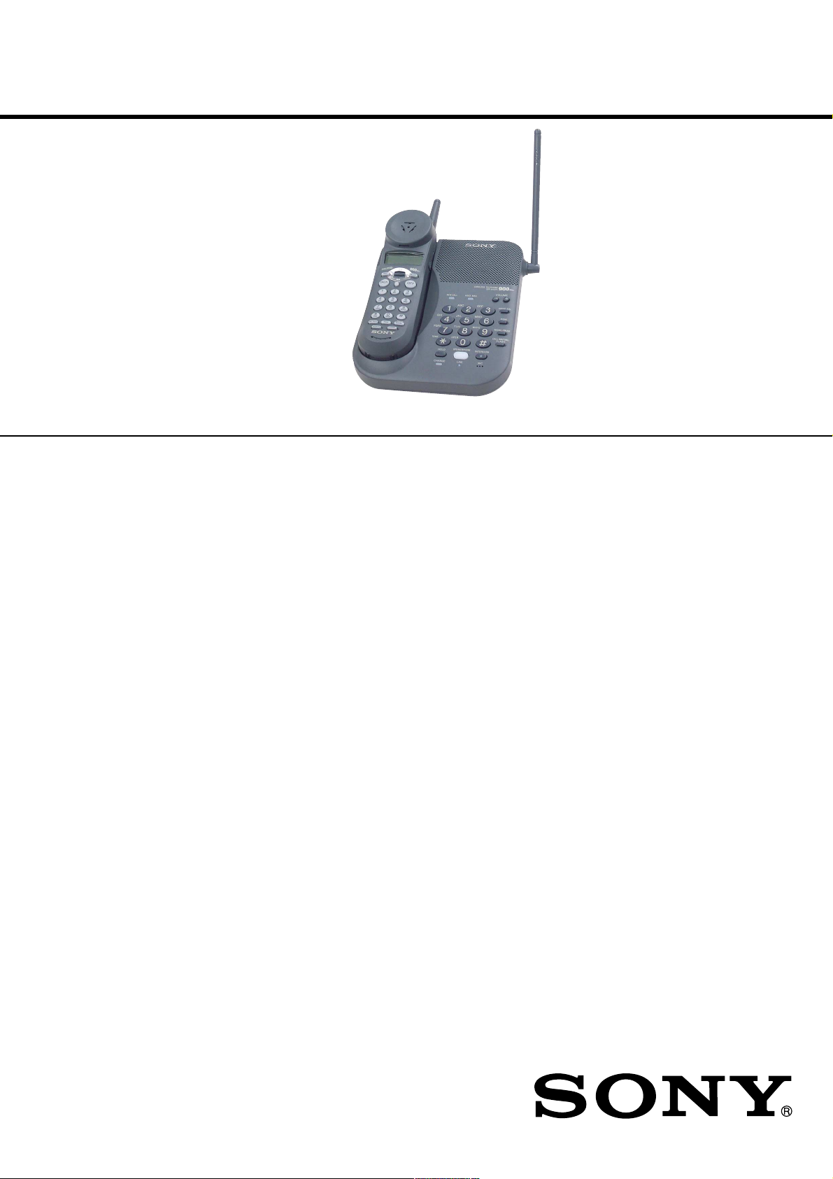
Photo: SPP-N1025
SPECIFICATIONS
General
Operating frequency
Base phone: 902-905 MHz (310µW)
Hand set: 925-928 MHz (400µW)
Operating channel
10 channels
Dial signal
Tone, 10 PPS (pulse) selectable
Supplied accessories
AC power adaptor AC-T122
Telephone line cord
Rechargeable battery pack BP-T18
Wall bracket
Directory
Canadian Model
Base phone
Power source
DC 9V from AC power adaptor AC-T122
Battery charging time
Approx. 12 hours
Dimensions
Approx. 7
antenna excluded
(approx. 175 x 57 x 190 mm)
Antenna: Approx. 6
(approx. 153 mm)
Mass
Approx. 13.5 oz (approx. 382 g), wall
bracket excluded
x 2 1⁄4 x 7 1⁄2 inches (w/h/d),
1
⁄ 8 inches
US Model
SPP-N1025
SPP-N1026
Handset
Power source
Rechargeable battery pack BP-T18
Battery life
Standby: Approx. 7 days
Talk: Approx. 7 hours
Dimensions
Approx. 2
antenna excluded
(approx. 55 x 47 x 183 mm)
Antenna: Approx. 1
(approx. 34 mm)
Mass
Approx. 7.7 oz (approx. 220 g), battery
included
9-873-224-02 Sony Corporation
2001L0500-1 Personal Audio Company
C 2001.12 Published by Sony Engineering Corporation
1
⁄4 x 1 7⁄8 x 7 1⁄4 inches (w/h/d),
3
⁄8 inches
Design and specifications are subject to
change without notice.
CORDLESS TELEPHONE
Page 2

SPP-N1025/N1026
TABLE OF CONTENTS
1. SERVICING NOTES............................................... 3
2. GENERAL ................................................................... 5
3. DISASSEMBLY
3-1. Disassembly Flow ........................................................... 6
3-2. H/S Rear Assy ................................................................. 6
3-3. H/S FRT Assy.................................................................. 7
3-4. HAND MAIN Board....................................................... 7
3-5. Base Bottom .................................................................... 8
3-6. BASE MAIN Board ........................................................ 8
4. TEST MODE.............................................................. 9
5. DIAGRAMS
5-1. Block Diagram – BASE UNIT Section –...................... 13
5-2. Block Diagram – HANDSET Section – ........................ 14
5-3. Note for Printed Wiring Boards and
Schematic Diagrams ....................................................... 15
5-4. Schematic Diagram – BASE MAIN Board (1/2) –....... 16
5-5. Schematic Diagram – BASE MAIN Board (2/2) –....... 17
5-6. Printed Wiring Board – BASE MAIN Board –............. 18
5-7. Printed Wiring Board – BASE KEY Board – ............... 19
5-8. Schematic Diagram – BASE KEY Board – .................. 19
5-9. Printed Wiring Board – HAND MAIN Board – ............ 20
5-10. Schematic Diagram – HAND MAIN Board – .............. 21
5-11. IC Pin Function Description ........................................... 22
6. EXPLODED VIEWS
6-1. Hand Set Section ............................................................. 24
6-2. Base Set Section.............................................................. 25
7. ELECTRICAL PARTS LIST ............................... 26
Notes on chip component replacement
• Never reuse a disconnected chip component.
• Notice that the minus side of a tantalum capacitor may be dam-
aged by heat.
SAFETY-RELATED COMPONENT WARNING!!
COMPONENTS IDENTIFIED BY MARK 0 OR DOTTED
LINE WITH MARK 0 ON THE SCHEMATIC DIA GRAMS
AND IN THE PARTS LIST ARE CRITICAL TO SAFE
OPERATION. REPLACE THESE COMPONENTS WITH
SONY PARTS WHOSE PART NUMBERS APPEAR AS
SHOWN IN THIS MANU AL OR IN SUPPLEMENTS PUBLISHED BY SONY.
ATTENTION AU COMPOSANT AYANT RAPPORT
À LA SÉCURITÉ!
LES COMPOSANTS IDENTIFIÉS P AR UNE MARQUE 0
SUR LES DIAGRAMMES SCHÉMATIQUES ET LA LISTE
DES PIÈCES SONT CRITIQUES POUR LA SÉCURITÉ
DE FONCTIONNEMENT. NE REMPLACER CES COMPOSANTS QUE PAR DES PIÈCES SONY DONT LES
NUMÉROS SONT DONNÉS DANS CE MANUEL OU
DANS LES SUPPLÉMENTS PUBLIÉS PAR SONY.
2
Page 3

SECTION 1
SERVICING NOTES
SPP-N1025/N1026
NOTE FOR REPLACEMENT OF THE EEPROM
The ID cord is written in the EEPROM.
When replacing the EEPROM, U6 on the B ASE MAIN board and
U4 on HAND MAIN board should be replaced together as a pair.
(Part No. X-3381-018-1)
PRIOR CHECK FOR SERVICING
This set can rewrite the ID number of handset to the ID number of
base unit in the test mode even their serial numbers are different.
You can find which is wrong, handset or base unit with this function.
Note: A normal set is needed for this test.
Define A as the normal set and B as the faulty set.
Disconnect their power.
Procedure:
1. Press the [PGM] key.
2. Select the “DIAL MODE” menu by pressing v or V keys.
3. Press the key sequence [SELECT], [2], [1], [0], [4].
4. When enter the test mode, happ y tone is emitted, and the LCD
displays as shown below.
ABOUT U7 ON THE BASE MAIN BOARD
U7 (Part No. 6-800-854-01) on the BASE MAIN board which has
board shape as shown below , is dif ferent from regular ICs in shape.
5. Press the key sequence [#], [2], [1], [1], [0] just after power
ON.
6. When enter the test mode, the [SPEAKERPHONE] LED and
[INTERCOM] LED light up, and happy tone is emitted.
7. Disconnect the po wer of the handset B, then connect the power
again.
8. Disconnect the power of the base unit A, then connect the po wer
again.
9. Cradle the handset B on the base unit A to charge the battery
of handset B for about 1 minute.
10. Press the [TALK] key of the handset B and join the base unit
A.
11. When joining is successful, the handset B is normal. But when
it fails, charge the battery of the handset B again.
12. Next, repeat the step 1 to step 9 with the handset A and base
unit B
13. When joining is successful with handset A and base unit B,
base unit B is normal and handset B is faulty.
3
Page 4
SPP-N1025/N1026
Ver 1.1
NEW/FORMER TYPE DISCRIMINATION
In this set with the following serial No. or later BASE MAIN and
HAND MAIN boards have been changed.
SPP-N1025 : Serial No. 0207433 or alter
SPP-N1026 : Serial No. A0106801 or later
Serial No.
Bottom View
NOTE FOR REPAIRING AND REPLACEMENT OF THE
NEW TYPE BO ARD
When a new type board is damaged or out of order, do not repair
that board, but replace with an former type board (BASE MAIN
board : Part No. A-3062-834-A, HAND MAIN board : Part No.
A-3062-832-A (N1025)/A-3062-877-A(N1026)). In this case, remove the EEPROM (BASE MAIN board : Ref No. U6, HAND
MAIN board : Ref No. U4) from the new type board and install it
on the former type board as a replacement.
– BASE MAIN BOARD (Conductor Side) –
U6
Serial No.
Bottom View
– HAND MAIN BOARD (Component Side) –
U4
Former T ype
U4
New Type
Lid Battery
4
Page 5

Identifying the parts
Refer to the pages indicated in parentheses for details.
Base Phone
1
2
3
4
5
6
7
8
9
1 VOICE MAIL lamp (p. 47)
Flashes when you have messages.
2 NEW CALL lamp (p. 39)
Flashes when there is a “NEW”
data in the Caller ID list.
3 Dialing keys
4 HOLD button (p. 20, 33)
Press to put a call on hold.
5 CHARGE lamp (p. 9, 19)
Lights while the battery is being
charged.
6 SPEAKERPHONE button
(p. 20, 22)
Press to make or receive a call with
the base phone.
This button keeps lit until you are
done talking.
7 LINE lamp (p. 18, 22)
Lights when the handset is in use.
8 MIC (microphone)
US
Getting Started
14
SECTION 2
GENERAL
0
qa
qs
qd
qf
qg
9 INTERCOM button/lamp
(p. 36)
Used to make an intercom call.
The INTERCOM lamp on this
button keeps lit until you are done
talking.
0 VOLUME +/– buttons (p. 20, 22)
Adjusts the speaker volume.
qa SPEED DIAL button (p. 25)
Used to make a call with speed
dialing.
qs PGM (Program) button (p. 25)
Used to store numbers for speed
dialing.
qd REDIAL/PAUSE button (p. 21)
Redials the last number called/
inserts a pause in the dialing
sequence.
qf RINGER switch (p. 32)
Used to adjust the ringer volume
level of the base phone.
qg CALL WAITING/FLASH button
(p. 20)
Switches to a second call if you
have “call waiting” service.
qh
qj
qh Antenna (p. 7, 49)
qj Speaker (p. 20, 22)
qk DC IN 9V jack (p. 7)
ql LINE (telephone line) jack
(p. 7)
SPP-N1025/N1026
This section is extracted from
instruction manual.
qk
ql
continued
Getting Started
Getting Started
US
15
Identifying the parts (continued)
Handset
1
2
3
4
5
6
1 Antenna
2 Speaker
3 Jog lever (p. 11, 23, 30, 31, 39)
4 HOLD button (p. 18, 34)
Press to put a call on hold.
5 TALK button (p. 18, 21, 22, 24,
33, 37)
Lets you make or receive a call.
6 Battery compartment (p. 9)
7
8
9
q;
qa
7 Display (p. 11, 38)
8 OFF button (p. 18, 22, 33, 35)
Allows you to disconnect the call.
9 Dialing keys
0 CHANNEL button (p. 18)
Press to select a better channel.
qa Microphone
qs
qd
qf
qg
qs FLASH button (p. 18, 46)
Switches to a second call if you
have “call waiting” service, or lets
you make a new call.
qd TONE button (p. 18)
Allows you to switch temporarily to
tone dialing.
qf ONE-TOUCH button (p. 23)
Used to make a call with one-touch
dialing.
qg INTERCOM button (p. 35)
Used to make an intercom call.
qh I (HEADSET) jack (p. 51)
qj SELECT button (p. 11 – 13, 23,
27, 31, 40, 42)
Press to enter the selection and
bring you to the next selection.
qh
qj
qk
ql
w;
qk # button (p. 44)
Used to change the number of digits
of the phone number in the Caller
ID list.
ql REDIAL/PAUSE button
(p. 21, 24, 26, 28)
Redials the last number called/
inserts a pause in the dialing
sequence.
w; PGM (Program) button
(p. 11 – 13, 23, 27, 31, 47)
Press to start the procedure for
setting up the phone such as
choosing the dialing mode.
Also used to store the setting to
finish the procedure.
Getting Started
US
16
Getting Started
Getting Started
US
17
5
Page 6
SPP-N1025/N1026
• This set can be disassembled in the order shown below.
3-1. DISASSEMBLY FLOW
SECTION 3
DISASSEMBLY
Set
Note: Follow the disassembly procedure in the numerical order given.
H/S rear assy H/S FRT assy
Base bottom
BASE MAIN board
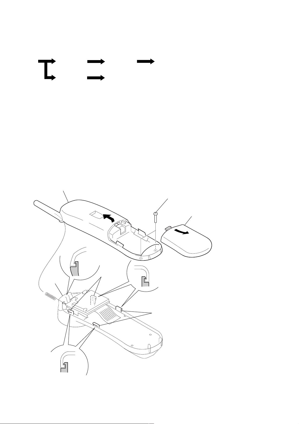
3-2. H/S REAR ASSY
5
Remove the H/S rear assy
in the direction of arrow
B
.
HAND MAIN board
2
two screws
(BTP3
×
10)
4
claw
B
3
two claws
3
two claws
A
1
Remove the battery lid
in the direction of arrow
A
.
6
Page 7

3-3. H/S FRT ASSY
d
3
screw
(BTP2.6
SPP-N1025/N1026
1
screw
(BTP2.6
×
8)
2
×
8)
4
two screws
(P2
×
5)
3-4. HAND MAIN BOARD
8
receiver BKT
6
H/S FRT assy
5
screw
(BTP2.6
×
8)
6
RF unit (hand)
5
2
speaker (2.8cm)
7
screw (BTP2.6 × 8)
1
Remove two solders of lead.
3
Remove solder of lead.
4
Remove twelve solders.
9
HAND MAIN boar
7
Page 8

SPP-N1025/N1026
)
3-5. BASE BOTTOM
3
base bottom
2
claw
1
five screws
(P3
×
12)
3-6. BASE MAIN BOARD
4
RF unit (base)
2
harness
1
Remove solder of lead.
2
claw
6
two screws
(BTP2.6
3
screw
(P3
8
×
8)
×
6)
BASE MAIN board
5
Remove two solders.
7
two screws
(BTP2.6
×
8
0
six screws
9
Remove two solders of lead.
qa
BASE KEY board
(BTP2.6
×
8)
8
Page 9

SECTION 4
TEST MODE
SPP-N1025/N1026
Introduction
The manual test mode can be used for testing the RF and audio
sections of the base unit and handset. The manual test mode is
also required for the FCC testing in which the phone is tested for
interference at the first, middle, and last RF channels.
The following features are provided in manual test mode.
• Able to set operating mode of the combo chip.
• Able to mute or unmute the audio path.
• Able to change the RF channel. (Both RX and TX)
• Able to transmit or receive data packet.
• Able to synchronize the security code.
BASE UNIT
1. Entering the Manual Test Mode
1. Press the key sequence [#], [2], [1], [1], [0] just after power
ON.
2. When enter the test mode, the [SPEAKERPHONE] LED and
[INTERCOM] LED light up, and happy tone is emitted.
2. Default Settings
• Channel set to 14. (out of 0 to 29)
• Combo set to active mode.
• Speakerphone unmute.
• TX audio path unmuted.
• RX audio path unmuted.
• TX power ON.
• Off hooked.
• Date transmission disabled.
3. SPEAKERPHONE Key Operation
1.
Condition: Press the
Operation: Toggle transmitter on/off, it only turn the TX power
on/off with no modulation.
Indication:Beep tone is emitted.
[1] key.
7.
Condition: Press the [7] key.
Operation: TX data on, it only send security code change command
out if the transmitter power ON.
Indication:Beep tone is emitted.
8.
Condition: Press the [8] key.
Operation: Base DTMF test, it will send the dight 3 DTMF to line.
Indication:Beep tone is emitted and DTMF 3 gen. in line.
9.
Condition: Press the [9] key.
Operation: Stop DTMF test, it will stop the DTMF to line.
Indication:Beep tone is emitted and stop DTMF.
10.
Condition: Press the [0] key.
Operation: Base will receive the handset security code change
command and toggle the [LINE] LED.
Indication:Beep tone is emitted and [LINE] LED is flashed.
11.
Condition: Press the [*] key.
Operation: Stop the data transmit, but don't turn the TX power
OFF.
Indication:Beep tone is emitted.
12.
Condition: Press the [#] key.
Operation: Increase the current channel to next, if 30 back to 1.
Indication:Beep tone is emitted.
13.
Condition: Press the
Operation: Generate current ringer.
Indication:Beep tone and ringer tone are emitted.
[REDIAL/PAUSE] key.
2.
Condition: Press the [2] key.
Operation: Toggle TX mute, it only toggle the TX path of combo
chip.
Indication:Beep tone is emitted.
3.
Condition: Press the [3] key.
Operation: Toggle mic mute pin, the mic mute pin defalt value in
test mode is high (mute).
Indication:Beep tone is emitted.
4.
Condition: Press the [4] key.
Operation: Toggle HF path switch function, the HF pin will be
toggle.
Indication:Beep tone is emitted.
5.
Condition: Press the [5] key.
Operation: Toggle RX mute function, it only toggle the TX path
of combo chip.
Indication:Beep tone is emitted.
6.
Condition: Press the [6] key.
Operation: Toggle spk mute pin, the spk mute pin defalt value in
test mode is low (unmute).
Indication:Beep tone is emitted.
14.
Condition: Press the [FLASH] key.
Operation: T oggle hook pin, the hook pin defalt value in test mode
is low (hook off).
Indication:Beep tone is emitted.
15.
Condition: Press the [HOLD] key.
Operation: Rewrite the EEPROM defalt value, ringer=1, flash
type=3 dialing type=tone, security code=000, last
channel=1.
Indication:Beep tone is emitted.
16.
Condition: Press the [INTERCOM] key.
Operation: T oggle telsw pin, the telsw pin defalt value in test mode
is low.
Indication:Beep tone is emitted.
17.
Condition: Press the [PGM] key.
Operation: Enable the base to reprogram the security code. After
press the [PGM] key, the base will wait the security
code change command within 2 second. If received,
the base security code will be reprogram.
Indication: Beep tone is emitted and if received the command
gen.happy tone is emitted after reprogram security code.
9
Page 10

SPP-N1025/N1026
18.
Condition: Press the [SPEED] key.
Operation: Cleaar all two touch memory from EEPROM.
Indication:Beep tone is emitted.
19.
Condition: Press the [SPEAKERPHONE] key.
Operation: Release thetestmode.
Indication:Beep tone is emitted.
4. Data Link
Data bits are encoded in manchester format for which bit “0” is
represented by 500 µs low and 500 µs high while bit “1” by 500
µs high and 500 µs low.
If data transmission is enabled, it will transmit data packet with
the following fields continuously.
(“0”=500 µs low and “1”=500 µs high)
• 8 bit preamble :0101010101010101
• 8 bit word sync :0110010010010110
• 20 bit security code :Restored from EEPROM
• 4 bit reserved data :01010101
• 8 bit command :0101010101010101
• 8 bit data :0101010101010101
If data transmission is enabled, it will toggle the [LINE] LED every
time when a data packet is received. (No security code would be
checked)
HANDSET
1. Entering the Manual Test Mode
1. Press the [PGM] key.
2. Select the “DIAL MODE” menu by pressing v or V keys.
3. Press the key sequence
4. When enter the test mode, happy tone is emitted, and the LCD
displays as shown below.
[SELECT], [2], [1], [0], [4].
[4] key
Operation: Increment channel by 1.
Indication:CH=CH+1
[5] key
Operation: Mute TX audio path.
Indication:TxM=1
[6] key
Operation: Mute RX audio path.
Indication:RxM=1
[7] key
Operation: Decrement channel by 1.
Indication:CH=CH–1
[8] key
Operation: Mute TX audio path.
Indication:TxM=0
[9] key
Operation: Mute RX audio path.
Indication:RxM=0
[0] key
Operation: Start LCD segment test.
Indication:Various patterns shown on LCD for a few seconds.
[*] key
Operation: Set combo to active mode.
Enable data transmission.
Indication:DA=1
[#] key
Operation: Disable data transmission.
Indication:DA=0
2. Default Settings
• Channel set to 14. (out of 00 to 29)
• Combo set to active mode.
(0: inactive mode, 1: RX mode, 2: active mode)
• TX audio path unmuted. (0: unmuted, 1: muted)
• RX audio path unmuted. (0: unmuted, 1: muted)
• Date transmission disabled. (0: disabled, 1: enabled)
• Battery detection.
(“E” icon on: RSSI detection, “E” icon off: battery detection)
3. Key Definition
[1] key
Operation: Set combo to inactive mode.
Indication:CB=0
[2] key
Operation: Set combo to RX mode.
Indication:CB=1
[3] key
Operation: Set combo to active mode.
Indication:CB=2
[ONE TOUCH] key
Operation: Switch to RSSI detection.
Indication:“E” icon turns off.
[REDIAL] key
Operation: Switch to battery detection.
Indication:“E” icon turns on.
[OFF] key
Operation: Release the test mode.
Note: All keys pressed will emit the key tone.
4. Data Link
Data bits are encoded in manchester format for which bit “0” is
represented by 500 µs high and 500 µs low while bit “1” by 500
µs low and 500 µs high.
If data transmission is enabled, it will transmit data packet with
the following fields continuously.
(“0”=500 µs low and “1”=500 µs high)
• 8 bit preamble :1010101010101010
• 8 bit word sync :1001101101101001
• 20 bit security code :Restored from EEPROM
• 4 bit reserved data :10101010
• 8 bit command :1010101010101010
• 8 bit data :1010101010101010
No matter data transmission is enabled or not, it toggles the
“NEW” icon every time when a data packet is received. (No security code would be checked)
10
Page 11

Security Code Synchronization
The following procedures should be followed if the security codes
of both unit do not match to each other.
1. Put the handset into manual test mode, making sure the channel
is set at 14 (default) out of 0 to 29.
2. Press the [*] key to start data transmission under which the
SC_SYNC command is sent continuously.
3. Put the base unit into manual test mode.
4. Before the base unit enters the manual test mode, it waits one
second for receiving SC_SYNC command from the handset.
If the command is received in the period, its security code will
be saved into EEPROM and then flash the [LINE] LED for
indication.
Frequency Allocation Tables
SPP-N1025/N1026
Base Unit Frequencies:
Channel
0 902.30 MHz 925.05 MHz 935.75 MHz
1 903.35 MHz 926.10 MHz 936.80 MHz
2 904.40 MHz 927.15 MHz 937.85 MHz
3 905.45 MHz 923.40 MHz 934.10 MHz
4 906.50 MHz 924.45 MHz 935.15 MHz
5 903.05 MHz 925.80 MHz 936.50 MHz
6 904.10 MHz 926.85 MHz 937.55 MHz
7 905.15 MHz 923.10 MHz 933.80 MHz
8 906.20 MHz 924.15 MHz 934.85 MHz
9 902.75 MHz 925.50 MHz 936.20 MHz
10 903.80 MHz 926.55 MHz 937.25 MHz
11 904.85 MHz 927.60 MHz 938.30 MHz
12 905.90 MHz 923.85 MHz 934.55 MHz
13 902.45 MHz 925.20 MHz 935.90 MHz
14 903.50 MHz 926.25 MHz 936.95 MHz
15 904.55 MHz 927.30 MHz 938.00 MHz
16 905.60 MHz 923.55 MHz 934.25 MHz
17 906.65 MHz 924.60 MHz 935.30 MHz
18 903.20 MHz 925.95 MHz 936.65 MHz
19 904.25 MHz 927.00 MHz 937.70 MHz
20 905.30 MHz 923.25 MHz 933.95 MHz
21 906.35 MHz 924.30 MHz 935.00 MHz
22 902.90 MHz 925.65 MHz 936.35 MHz
23 903.95 MHz 926.70 MHz 937.40 MHz
24 905.00 MHz 927.75 MHz 938.45 MHz
25 906.05 MHz 924.00 MHz 934.70 MHz
26 902.60 MHz 925.35 MHz 936.05 MHz
27 903.65 MHz 926.40 MHz 937.10 MHz
28 904.70 MHz 927.45 MHz 938.15 MHz
29 905.75 MHz 923.70 MHz 934.40 MHz
Transmit Receive RX LO
Frequency Frequency Frequency
Handset Frequencies:
Channel
00 925.05 MHz 902.30 MHz 891.60 MHz
01 926.10 MHz 903.35 MHz 892.65 MHz
02 927.15 MHz 904.40 MHz 893.70 MHz
03 923.40 MHz 905.45 MHz 894.75 MHz
04 924.45 MHz 906.50 MHz 895.80 MHz
05 925.80 MHz 903.05 MHz 892.35 MHz
06 926.85 MHz 904.10 MHz 893.40 MHz
07 923.10 MHz 905.15 MHz 894.45 MHz
08 924.15 MHz 906.20 MHz 895.50 MHz
09 925.50 MHz 902.75 MHz 892.05 MHz
10 926.55 MHz 903.80 MHz 893.10 MHz
11 927.60 MHz 904.85 MHz 894.15 MHz
12 923.85 MHz 905.90 MHz 895.20 MHz
13 925.20 MHz 902.45 MHz 891.75 MHz
14 926.25 MHz 903.50 MHz 892.80 MHz
15 927.30 MHz 904.55 MHz 893.85 MHz
16 923.55 MHz 905.60 MHz 894.90 MHz
17 924.60 MHz 906.65 MHz 895.95 MHz
18 925.95 MHz 903.20 MHz 892.50 MHz
19 927.00 MHz 904.25 MHz 893.55 MHz
20 923.25 MHz 905.30 MHz 894.60 MHz
21 924.30 MHz 906.35 MHz 895.65 MHz
22 925.65 MHz 902.90 MHz 892.20 MHz
23 926.70 MHz 903.95 MHz 893.25 MHz
24 927.75 MHz 905.00 MHz 894.30 MHz
25 924.00 MHz 906.05 MHz 895.35 MHz
26 925.35 MHz 902.60 MHz 891.90 MHz
27 926.40 MHz 903.65 MHz 892.95 MHz
28 927.45 MHz 904.70 MHz 894.00 MHz
29 923.70 MHz 905.75 MHz 895.05 MHz
Transmit Receive RX LO
Frequency Frequency Frequency
11
Page 12

SPP-N1025/N1026
MEMO
12
Page 13

SECTION 5
DIAGRAMS
5-1. BLOCK DIAGRAM – BASE UNIT Section –
MIC101
MIC
SP101
A1
SPEAKER AMP
OUTPUT1
3
OUTPUT2
6
MUTE
RF UNIT
ANT TX AUDIO
RX AUDIO
TX DATA
RX DATA
PLL DATA
PLL CLK
PLL EN
CAR DET
VOICE SPEAKERPHONE
U4
MIC MICO
MIC
11 10 9 7
AMP
MUTE
12
U14
RECO
7
INPUT+
1
2INPUT–
TI TO
ATTENUATOR
TLI2
17
RLI2
20
DIAL MODE
DETECTOR
RX
ATTENUATOR
TX
ATTENUATOR
CONTROL CIRCUIT
RI
2122
8
LEVEL
DETECTOR
PD
1
4
TEL LINE
SWITCH
U13 (2/4)
5
FILTER
AMP
VCI
HTI
SPP-N1025/N1026
TEL LINE
SWITCH
U13 (3/4)
AF AMP
9
3
HTO+
HYBRID
HTO–
AMP
13
SPEAKER ON/OFF
FI
2
2
6
TLI1
RLI1
SWITCH
U13 (1/4)
13
8
5
6
23
26
1
+
AF AMP
(FOR SPEAKER)
U2 (3/4)
16
(FOR TX)
U2 (1/4)
AF AMP
(FOR RX)
U2 (2/4)
FREQUENCY SHIFT
KEYING DEMODULATOR
U3
DTMF
OUT
DC COMPA
XIN
4
5
X1
3.58MHz
SW1
RINGER
KEY MATRIX
KEY1 – 17,
KEY19 – 22
IN SE
IN P
IN N
IN DSP
IN DCN
M DAT
SCK
SD IN
SD OUT
INT
DCB RD
XOUT
9
10
11
13
14
24
23
22
21
20
1
2
OFF
LOW
HIGH
D11
D10
D9
D13
BUFFER
Q1
AF AMP
(FOR DTMF)
U2 (4/4)
64
53 TX DATA
11
50
49
48
52
45
44
38 VOL1
39 VOL2
40
13
1
43
63
2
TEL SWITCH
RX DATA
PLL DATA
PLL CLK
PLL EN
CAR DET
RI LO
RI HI
ROW0 – ROW5
33 – 36 3 – 8
COL0 – COL3
VOL3
SP SW
MIC MUTE
RINGER
RO LO
SPK MUTE
14
57 58 59 60 61
DCA
DCB RD
SYSTEM
CONTROLLER
U7
T2
LINE TRANSFORMER
MDAT
CIDINT
CIDSCL
CIDSDA
INTCOM LED
N MSG LED
XOUT
XIN
2322
X2
8MHz
OFF HOOK
EE DO
EE DI
EE CLK
EE CS
LINE LED
SPK LED
WAIT LED
CHRG LED
PARK
FST CHG
D14 D16
D15 D7
HOOK ON/OFF
U8
J7
LINE
• SIGNAL PATH
: TX
: RX
: BELL
KEY16 KEY17 KEY22
HOLD
KEY13 KEY 14 KEY15
KEY10 KEY11 KEY12 KEY20
PQRS 7 WXYZ 9
GHI 4
25
54
42
41
55
26
27
28
29
30
31
21RESET
9
10
CHARGE
DETECT
Q4
4
DO
3
DI
2
CLK
1
CS
SPEAKERPHONE
INTERCOM
NEW CALL
VOICE MAIL
CHARGE
RESET SIGNAL
GENERATOR
Q5, 6
CHARGE
CONTROL
Q2, 8
B+
(+5V)
1
LED7
LINE
LED6
LED8
LED2
LED4
LED1
SPEAKERPHONE
OPER 0 TONE
TUV 8
KEY 8KEY 7
JKL 5
KEY5KEY4
ABC 2
EEPROM
U6
+5V
REGULATOR
U5
INTERCOM
#
KEY 9
MNO 6
DEF 3
KEY3
VOLUME+
KEY21
CALL WAITING/
FLASH
REDIAL/
PAUSE
KEY2
PGM
KEY1KEY6
SPEED DIAL
KEY19
–
+
CHARGE
TERMINAL
–
J3
–
DC IN 9V
+
1313
Page 14

SPP-N1025/N1026
5-2. BLOCK DIAGRAM – HANDSET Section –
A2
RF UNIT
• SIGNAL PATH
RF
TX DATA
PLL EN
PLL CLK
PLL I2C DATA
RX DATA
CAR DET/LOW BAT
MIC
EARO
EEPROM
U4
5SDA
6SCL
SP1
J8
I
MIC1
29 TX DATA
14 PLL EN
15 PLL CLK
16 PLL I2C DATA
17 I2C CLK
11 RX DATA
12 CAR DET
SYSTEM
CONTROLLER
U2
79 – 94
COM0 – COM15
78 – 32
SEG0 – SEG46
27BUZZER
30BACK LIGHT
(N1026)
BUZZER
DRIVE
Q4
D5, 6
(LCD BACK LIGHT)
D14 – 17
(KEY BACK LIGHT)
LCD1
LIQUID CRYSTAL
DISPLAY MODULE
LED DRIVE
BUZ1
B+
Q2
: TX
: RX
KEY MATRIX
K1 K2 K3
1
K4 K5 K6
4 GHI
7 PQRS 9 WXYZ
TONE
K13
ONE TOUCH
5 JKL
K7 K8 K9
8 TUV
K10K11
0 OPER
K14
PGM
REDIAL
K1 – 22,
SW1, 2
K16 SW1
3 DEF
6 MNO
PAUSE
TALK2 ABC
K17
FLASH
K12 SW2
K22
INTERCOM
#
K20K15
CHANNEL
VOL V
CID
K21
SELECT
K19
HOLD
VOL v
DIR
K18
OFF
D10 – 12
19 – 21, 28
COL0 – COL3
22 – 26
ROW0 – ROW4
13 KEY INT
2
XTIN3XTOUT
X2
8MHz
XTIN7XTOUT
6
X1
32.768kHz
9CRADLE
CRADLE
DETECT
Q1
D2
+
RESET SIGNAL
8RESET
GENERATOR
Q3, 5
D7
CHARGE
TERMINAL
–
95V4
96V3
97V2
98V1
+2.3V
REGULATOR
U3
RECHARGEABLE
BATTERY PACK
(BP-T18)
3.6V 600mAh
1414
Page 15

SPP-N1025/N1026
p
p
p
1
3
4
5
6
9
10
12
24
23
22
21
20
19
18
17
16
15
14
13
SELECT
SWITCH
SERIAL
INTERFACE
+
–
+
–
CRYSTAL
OSCILLATOR
REFERENCE
GENERATOR
7
+
–
+
–
+
–
11
SELECT
ADC
BAND PASS FILTER CAS DETECTOR
FSK RECEIVERBAND PASS FILTER
BAND PASS FILTER
DIAL TONE
ENERGY DETECTOR
DIAL TONE
DETECTOR
RING DETECTOR
DC MEASUREMENT
UNIT
DC B
DC A
ADC
+
–
DTMF
GENERATOR
D/A CONVERSION
AND FILTERING
MDAT
SCK
SDIN
SDOUT
INT
RESET
VDDP
VDDA
DTMFOUT
OUTDC
INDCN
INDCP
DCB RD
VDDD
XIN
XOUT
VSSD
VREF
INSE
INP
OUT
VSSA
INN
8
2DCCOMPA
2
1
RLO1
TLO1
TLI1
RLI1
CPR
GND
RXO
RXI
RLI2
RLO2
TLO2
TLI2
CPT
VB
FI
4
VCC
3
CD
FO
+
–
+
–
5
9
8
7
6
HTI
TXO
TXI
HTO+
HTO–
10
12
11
14
13
27
28
2526
24
20
21
22
23
19
17
18
15
16
MUT
MCO
MCI
CT
VLC
VR
VCC
HYBRID
AMP 2
HYBRID
AMP 1
MIC
AMP
VREF
+
–
VR
FILTER
AMP
COMPARATOR
AGC
BACKGROUND
NOISE
DETECTOR
VR
LEVEL
DETECTOR
LEVEL
DETECTOR
COMPARATOR
ATTENUATOR
CONTROL BLOCK
BACKGROUND
NOISE
DETECTOR
DIAL
TONE
DETECTOR
LEVEL
DETECTOR
LEVEL
DETECTOR
RX
ATTENUATOR
TX
ATTENUATOR
5-3. NOTE FOR PRINTED WIRING BOARDS AND SCHEMATIC DIAGRAMS
Note on Printed Wiring Board:
• X : parts extracted from the component side.
• Y : parts extracted from the conductor side.
z
•
: Through hole.
• : Pattern from the side which enables seeing.
• : Carbon pattern.
(The other layers' patterns are not indicated.)
Caution:
Pattern face side: Parts on the pattern face side seen from
(Conductor Side) the pattern face are indicated.
Parts face side: Parts on the parts face side seen from
(Component Side) the parts face are indicated.
Note on Schematic Diagram:
• All capacitors are in µF unless otherwise noted. pF: µµF
50 WV or less are not indicated except for electrolytics
and tantalums.
• All resistors are in Ω and 1/
specified.
4
• % : indicates tolerance.
• C : panel designation.
• A : B+ Line.
• Power voltages are dc 9 V and fed with regulated dc pow er
supply from external power voltage jack (J3) on the BASE
MAIN board, dc 12 V and fed with regulated dc power
supply from modular jack (J7) on the BASE MAIN board
with 100 Ω in series, and dc 3.6 V and f ed with regulated
dc power supply from battery terminal (J5) on the HAND
MAIN board.
• Voltages and wa vef orms are dc with respect to ground in
test mode.
• Voltages are taken with a V OM (Input impedance 10 MΩ).
Voltage variations may be noted due to normal production tolerances.
• Waveforms are taken with a oscilloscope.
Voltage variations may be noted due to normal production tolerances.
• Circled numbers refer to waveforms.
• Signal path.
N : RX
O : TX
P : BELL
• IC Block Diagrams – BASE MAIN Board –
U3 PCC318
W or less unless otherwise
• Waveforms – BASE MAIN Board –
1 U7 wd (XOUT)
1 V/DIV, 50 ns/DIV
2 U3 5 (XOUT)
500 mV/DIV, 100 ns/DIV
279 ns
125 ns
– HAND MAIN Board –
qa U2 3 (XOUT)
3.9 Vp-
1 Vp-p
1 V/DIV, 50 ns/DIV
qs U2 7 (XTOUT)
1 V/DIV, 20 µs/DIV
125 ns
30.5 µs
3.9 Vp-
2.4Vp-
U4 U4082B
1515
U14 KA8602D
BIAS
CIRCUIT
IN+
1
IN–
2
+–
OUT1
VCC
AMP1 AMP2
3
4
RIPPLE
8
REJECTION
7
MUTE
+–
6
OUT2
5
GND
Page 16

SPP-N1025/N1026
5-4. SCHEMATIC DIAGRAM – BASE MAIN Board (1/2) –• See page 15 for Waveforms. • See page 15 for IC Block Diagram.
SW1
RINGER
OFF
LOW
HIGH
T
2
3
A
A
D
L
D
M
C
SD
S
ID
ID
C
C
SYSTEM CONTROLLER
R58
1M
C32
47p
T
IN
ID
C
TMP87CH41U
47p
31
C
R
S
B
C
C
D
U7
1%
z
H
120
360
8M
64
47
X2
R
R
E
K
P
LIN
S
T
O
T
T
K
E
A
L
A
D
-C
-D
-D
-D
T
P
C
P
PLL EN
C55 R87
47p 10k
RI_LO
RI_HI
DI
CLK
X5
X6
X7
COL3
COL2
COL1
COL0
1%
1%
1%
1%
330
330
330
330
74
65
75
51
R
R
R
R
M
O
G
C
IT
G
R
T
A
S
H
IN
M
W
C
R88
10k
R25
47k
10k
49
R
R26
R48
10k
10k
CS
CLK
DI
DO
CS
CLK
DI
DO
93C46D
EEPROM
U6
VCC
NC1
VSS
C30
0.1
NC
X
X
R127
0
R73
47k
R67
ROW0
ROW1
ROW2
ROW3
ROW4
ROW5
R-DAT
DCA
0
X1
X8
R24
47k
Q5,6
RESET SIGNAL
GENERATOR
R43
62k
R44
15k
R46Q4
100kMMBT3904
R45
47k
Q6
MMBT3904
Q5
MMBT3904
C28R42
0.130k
R72
47k
R99
0
C29
0.1
R60
22k
MMBT3904
R61
10k
1%
R63
47k
R62R38
2708.2k
Q8
Q2
MMBT3904
Q2,8
CHARGE
CONTROL
R52
330
1%
RI_LO
RI_HI
R39
10k
R40
2.2k
CHARGE
DETECT
R41
100k
1
2
3
POWER SUPPLY
(12V)
5
6
(Page 17)
4700p
R4
3.6k
EC7
2.2
50V
R15 U2(1/4)
R5R6
5.1k LM324
2.2k68
EC2
1
50V
R11
750
R19
C58C57
2kV
R133R129
220k220k
R17
C6
100k
1%
0.1
R20
10k
15k
C19
6800p
R31
47k
R77
0
C12
56p
C20
56p
R23
68k
AF AMP(FOR TX)
EC3
4.7
50V
EC4
4.7
50V
R7
360k
R14
470k
AF AMP(FOR RX)
AF AMP(FOR DTMF)
(1/4)
U2(2/4)
LM324
(2/4)
C18
56p
R30
Z4Z3
DTZ5.6DTZ5.6
R16
5.1k
100k
U2(4/4)
LM324
(4/4)
C40
3300p
D5
BAV99L
C13
0.22
C17
0.1
X1
3.58MHz
R22
C11
56p
100k
R108
18k
R110
U2(3/4)
LM324
AF AMP(FOR SPEAKER)
DCB RD
DCA
27k
(3/4)
PCC318
DCB_RD
DC_COMPA
VDD_D
XIN
XOUT
VSS_D
VSS_A
VREF
IN_SE
IN_P
IN_N
OUT
FREQUENCY SHIFT
KEYING DEMODULATOR
U3
M_DAT
SD_OUT
VDD_P
VDD_A
OUT_DC
IN_DCN
IN_DCP
SD_IN
RESET
SCK
INT
DTMF
_OUT
CIDSCL
CIDSDA
CIDINT
MDAT
A1
A2
A3
R34
3k
R35
3k
R32C16 C15
220k56p 56p
C23 C22 C21
0.1 0.1 0.1
R2
0
Q1
Z2 R3
DTZ5.6
R132 R135
5.1M 5.1M
2
3
A
A
MMBT3904
BUFFER
390
4700p
2kV
R98 R134
220k 220k
R130R131
5.1M5.1M
R28R29 R21
51k51k 220k
R12
3.3k
U8
U5
IN OUT
GND
EC6
50V
10
TLP627
HOOK
ON/OFF
LINE
TRANSFORMER
T2
1
A
J7
LINE
100Ω
+
-
CHARGE
TERMINAL
-
+
J3
DC IN 9V
L7
10µH
D8
F2
L8
250mA
10µH
250V
L6
10µH
L5
10µH
Z5
DTZ27
D7
U05G
D16
U05G
D15
U05G
D14
U05G
+5V REGULATOR
EC5
1000
16V
NJM78M05FA
C26 C24
0.1 0.1
L3
10µH
L1
10µH
7
8
9
10
11
12
13
14
15
The components identified by mark 0 or dotted
line with mark 0 are critical for safety.
Replace only with part number specified.
Les composants identifiés par une marque 0 sont
critiques pour la sécurité. Ne les remplacer que
par une pièce portant le numéro spécifié.
1616
Page 17

5-5. SCHEMATIC DIAGRAM – BASE MAIN Board (2/2) –• See page 15 for IC Block Diagrams.
SPP-N1025/N1026
(Page 16)
1
2
C44
0.1
VOICE SPEAKERPHONE
U4
R114
24k
R109
27k
R115
220k
C41
47p
X1
X5
X6
X7
3
5
6
7
8
D9 R69
1N4148 15k
D10
1N4148
D11
1N4148
R120
R70
33k
R71
68k
9.1k
R121
6.2k
EC17 EC8 EC9
1 50V 4.7 50V 100 16V
C47
1000p
C48
0.1
R111
10k
C42
0.1
C50R112
0.110k
C43
220p
R113
R68
120k
24k
R119
56k
C27
0.1
C34
1000p
U4082B
PD
FI
CD
VS
HTO+
HTO-
HTI
TO
TI
MICO
MIC
MUTE
VCI
CT
R116
4.7k
C46C45
0.10.01
R78
C49
5.1k
47p
47
50V100k
2.2 50V
2.2 50V
EC14EC18
EC15
EC16
2.2 50V
EC12
47
16V
R118
50V
2.2
50V
R117
R95
8.2k
R83
C53
0.1
EC11
EC10
220k 100k
GND
CPR
RLI1
RLO1
TLO1
TLI1
RECO
RI
RLI2
RLO2
TLO2
TLI2
CPT
VB
C51
3300p
EC13
10
50V
C54
0.1
EC19
1
50V
10
C52
3300p
X8
SPEAKER AMP
U14
R85
33k
R79
15k
D13 R33
X3
1N4148 22k
U13(1/4)
MC54/74HC4066
KA8602B
INPUT+
INPUT-
OUTPUT1
VCC
R81 C37
47k 1000p
RIPPLE
OUTPUT2
R86
33k
EC22
10
REJ
MUTE
GND
R10
R80
180k
360k
C38
1000p
R91
120k
R92
39k
50V
R82
180k
C39
330p
MIC101
MIC
J2
1
T-DAT
C-DET
PLL EN
R93
68k
R90R9C10
150k47k4.7
R103
47k
P-CLK
P-DAT
R-DAT
TX DATA
RX AUDIO
CAR DET
MCU CLK
PLL EN
PLL CLK
PLL DATA
RX DATA
TX AUDIO
VREG
GND
GND
12
A1
RF UNIT
(1/4), (2/4)
U13(2/4)
MC54/74HC4066
9
10
11
12
13
14
15
R18
430k
R8
91k
R89
0
R96
1
R1 R94
00
EC1 EC20
100
16V
C25 C2
0.1 0.1
C9
0.01
C8
0.22
100
16V 0
X2
R66
TEL LINE
SWITCH
R104
9.1k
J4
U13(3/4)
MC54/74HC4066
R124
15k
R122
15k
VCC
GND
U13(4/4)
MC54/74HC4066
SPEAKER ON/OFF
SWITCH
(3/4)
R101
0
R27
0
R107
15k
INTCOM
R125
COL2
15k
ROW0
ROW2
ROW5
R76
LINE
15k
SPK
COL1
ROW4
ROW3
ROW1
R123
15k
CHRG
COL0
COL3
WAIT
MSG
R36
INTCOM LED
HOLD LED
CHRG LED
0
N MSG LED
LINE LED
SPK LED
WAIT LED
ROW0
ROW2
ROW5
ROW4
ROW3
ROW1
SPK(+)
SPK(-)
1
COL2
VREG
COL1
(Page 19)
VREG
COL0
COL3
GND
22
1717
Page 18

SPP-N1025/N1026
5-6. PRINTED WIRING BOARD – BASE MAIN Board –
1 2 3 4 5 6 7 8 9 10 11 12
BASE MAIN BOARD
A
D
G
H
R134
R98
R135
D8
C57C58
B
L7
L8
R132
F2
C
J7
LINE
6
4
2
1
3
5
J3
+
–
Z5
DC IN 9V
E
L1
F
• Semiconductor Location
Ref. No. Location
D5 B-5
D7 C-3
D8 B-2
D9 D-10
D10 D-10
D11 E-10
D13 D-6
D14 C-3
I
D15 C-3
D16 C-3
T2
LINE
TRANSFORMER
EC20
+
C2
R66
EC5
C26
R96
1
U5
Ref. No. Location
Q1 D-3
Q2 B-7
Q4 B-8
Q5 F-9
Q6 E-9
Q8 B-7
U2 D-5
U3 B-6
U4 G-8
U5 F-3
3
Q1
ECB
+
1
R3
Z2
L3
R133
R129
R131
R130
D14
D16
D7
D15
R5
R6
R4
R12
R11
+
EC2
R1
EC6
C24
+
RF
UNIT
Ref. No. Location
U6 B-9
U7 D-9
U8 C-4
U13 E-5
U14 H-7
Z2 E-3
Z3 B-7
Z4 B-7
Z5 D-2
R39
R40
+
+
C29
EC11
R38R60
49
U7
EC12
+
R24
U6
45
R26
R49
1
8
R88
R101
48
17
X2
C28
ECB
Q6
EC8
EC9
+
+
R68
C43
R119
C27
R113
C50
R112
C42
R111
C44
R116
C45
R114
HIGH
R72
R73
R58
C31
C32
R44
R115
R67
SW1
RINGER
LOW
R63
33
32
ECB
R43
R117
R109
R62
Q2
C30
64
1
15
R61
R41
ECB
Q4
C48
R95 C51
R48
C55
R87
16
14
U4
28
C49
8
+
5
EC22
R86
C54
1
C47
C46
R78
R118
Q5
R45
OFF
R46
D11
L5
L6
D10
R71
D9
R70
R69
R75
R51
R47
R64
R65
R36
R74
35-4752-04-
CHARGE
TERMINAL
A
BASE KEY
BOARD
J2
MIC101
MIC
C34
R121
R123
R107
R122
R99
EC17
R120
+
22
(Page 19)
R76
R124
R125
1
J4
00
R22
C12
R23
C11
C15
R21
R28
R29
U8
C16
R2
D5
K/A
R77
K
R32
A
R35
R34
C22
24
C21
1213
U3
1
C13
Z3 Z4 R52
R42
ECB
Q8
X1
R80
C37
R81
R25
C23
R33
C17
D13
EC7
+
C9
R18
R30
EC4
1
R7
R19
R20
R15
7
U2
R17
EC3
+
C6
C19
R31
R8
R94
J2
C8
R91
12
A1
C18
14
8
R14
+
C20
C40
R108
R110
R16
71
R9 C10
C41
R104R92
U13
8
14
R103
R90
R93
R127
EC16
R54
C25
EC15
C38
EC14
R27
EC1
+
EC10
+
+
C53
C52
R84
+
EC18
R79
R83
C39
R82
R10
R85
EC19
+
1
4
U14
+
+
EC13
1818
Page 19

SPP-N1025/N1026
J6
5-8. SCHEMATIC DIAGRAM – BASE KEY Board –5-7. PRINTED WIRING BOARD – BASE KEY Board –
(Page 18)
(Page 17)
• Semiconductor
Location
Ref. No. Location
LED1 H-2
LED2 B-2
LED4 B-3
LED6 G-3
LED7 H-3
LED8 G-5
1919
Page 20

SPP-N1025/N1026
MODULE
3.6V 600mAh
0
5-9. PRINTED WIRING BOARD – HAND MAIN Board –
• Semiconductor
Location
Ref. No. Location
D1 C-9
D2 C-8
D3 B-8
D4 A-3
D5 C-1
D6 B-1
D7 C-8
D10 B-6
D11 B-6
D12 B-6
D14 F-5
D15 G-7
D16 G-5
D17 F-7
D21 C-5
Q1 C-8
Q2 A-3
Q3 B-4
Q4 C-9
Q5 B-4
U2 B-3
U3 C-5
U4 A-4
1
CHARGE
TERMINAL
2020
Page 21

5-10. SCHEMATIC DIAGRAM – HAND MAIN Board –• See page 15 for Waveforms.
J3
1
V BAT
A2
CHARGE
TERMINAL
RECHARGEABLE
BATTERY PACK
3.6V 600mAh
UNIT
SP1
(BP-T18)
TX DATA
MIC
GND
CAR DET/LOW BAT
RF
J8
PLL EN
PLL CLK
PLL I2C DATA
RX DATA
GND
EARO
12
C66
220p
R43
10
R42
C35
220p
J9
2
1
+
-
J5
2P
10
MIC1
A1
A3
A4
R54
A5
15k
A6
R45
10k
R44
33
EC3
10
16V
TP4
R36
1.8k
TP1
C1
100p
R52
2.2k
+2.3V REGULATOR
U3
R12
7.5k
C8
0.1
C24
100p
C28
100p
PQ1R23
CTRL
GND1
BYP
ESD1
R24
18k
R25
18k
ESD2
R55
33k
TP5
R57
1k
EC2
10
16V
COM2
COM3
COM4
COM5
COM6
COM7
COM8
COM9
COM10
COM11
COM12
COM13
COM14
COM15
C11
Q1
MMBT3904
CRADLE
DETECT
0.22
C9
0.22
C10
0.22
C12
0.22
C13
0.22
X2
8MHz
R33
1M
C26
47p
C7
0.1
D21
BAS16
VCC
GND2
OUT
R3
1k
100k
R14
33k
C14
0.1
TP3
R41
TP2
47k
R1
100k
R2
D2
BAV99L
D7
BAV99L
R11
47k
R10
1M
C6
100p
MMBT3904
C5C4C2 C3
R9D3
91kHZK6A
0.14.70.1 0.1
RESET SIGNAL GENERATOR
SPP-N1025/N1026
0
1
M
O
C
1
M
CO
COM2
COM3
COM4
COM5
COM6
COM7
COM8
COM9
COM10
COM11
COM12
COM13
COM14
COM15
V4
V3
V2
V1
C1
C0
S
VS
EC1
C15C16C27
16V0.147p47p
Q5
Q3,5
M
O
C
0
M
CO
IN
X
47
MMBT3904
3
0
1
2
G
G
G
G
E
E
E
E
S
S
S
S
0
3
2
G
EG1
EG
EG
S
SE
S
S
T
T
U
D
IN
O
D
TES
X
XT
V
X1
32.768 kHz
C19C18
22p22p
R7R6
560k820k
Q3
8
5
6
9
7
4
G
G
G
G
G
E
E
E
E
E
S
S
S
S
S
7
6
5
G4
SE
T
U
XTO
8
EG
EG
EG
SEG
S
S
S
LE
ATA
D
ET
D
X
ES
RA
ATE IO
R
R
C
6
A
0
1
G
E
G
S
E
S
9
10
SEG
SEG
SYSTEM CONTROLLER
TMP87C807U-3CR4
T
ET
D
EY IN
K
CAR
1
A
R31
100k
B7
B8
B9
3
5
12
SEG
U2
LK
PLL C
1
G
E
S
5
A
3
EG1
S
TA
A
L I2C D
PL
DAP202K
DAP202K
6
7
4
1
1
1
1
G
G
G
G
E
E
E
E
S
S
S
S
14
16
15
G
EG
SEG
S
SE
LK
L0
REF
O
A
C
I2C C
V
R26
47k
3
2
B
B
D12
D11
DAP202K
D10
1
2
1
1
G
G
E
E
S
S
G11
SE
LL EN
P
4
3
A
A
1
2
0
8
9
2
2
2
1
1
G
G
G
G
G
E
E
E
E
E
S
S
S
17
EG
S
L1
O
C
4
B
S
S
20
22
18
G21
G19
EG
EG
S
SEG
SE
SE
S
1
2
3
0
2
W
W
W
W
L
O
O
O
O
CO
R
R
R
R
8
7
B
B
R32
100k
100k
100k
R30
R29
7
4
3
5
6
2
2
2
2
2
G
G
G
G
G
E
E
E
E
E
S
S
S
S
S
100k
5
26
2
23
24
27
SEG
SEG
SEG
SEG
SEG
SEG28
SEG29
SEG30
SEG31
SEG32
SEG33
SEG34
SEG35
SEG36
SEG37
SEG38
SEG39
SEG40
SEG41
SEG42
SEG43
SEG44
SEG45
SEG46
4
W
ZZER
O
R
BU
9
B
R27
100k
100k
R28
NC
L3
BACK
X DATA
LIGHT
CO
T
TP7
0
1
B
TP8
TP9
SEG28
SEG29
SEG30
SEG31
SEG32
SEG33
SEG34
SEG35
SEG36
SEG37
SEG38
SEG39
SEG40
SEG41
SEG42
SEG43
SEG44
SEG45
SEG46
R38
100k
R37
100k
R34
0
K1 K2
1 TALK
K4
4 GHI
7 PQRS
K11 K10
*
2
B
8 TUV 9 WXYZ
0 OPER TONE
C20
0.1
R22
R40
0
Q4
MMBT3906
BUZZER DRIVE
BAS16
R5
1k
R15
18
BAV99L
R16
680
(N1026)
R17
12
5
A
K3 K16
3 DEF2 ABC
K5 K6
K14K13 K20
6 MNO5 JKL
K9K8K7
K12
#
K15
K15
PAUSE
REDIAL
3
B
4
B
U4
24WC32
VCC
A0
WP
A1
SCL
A2
SDA
GND
EEPROM
R4
15
D1
Q2
MMBT3906
LED DRIVE
D4
14
15
D
D
TF541M
TF541M
D14-17
(KEY BACK LIGHT)
D5,6
(LCD BACK LIGHT)
D5 D6
K17
FLASH
K22
INTERCOM
CHANNELONE TOUCH PGM
J4
COM0
COM1
COM2
COM3
COM4
COM5
COM6
SEG5
SEG6
SEG7
SEG8
SEG9
SEG15
SEG16
BUZ1
R49R46 R47 R48
2727 27 27
D17
D16
TF541M
TF541M
R18
27
SW1
VOL
CID
K21
SELECT
K19
HOLD
SW2
VOL
DIR
K18
OFF
0
1
B
SEG17
SEG18
SEG19
SEG25
SEG26
SEG27
SEG28
SEG29
SEG30
SEG31
SEG32
SEG33
SEG34
SEG35
SEG36
SEG37
SEG38
SEG39
COM14
COM15
COM10
COM9
COM8
COM7
COM1
COM2
SEG40
SEG41
SEG42
SEG43
SEG44
SEG45
SEG46
COM0
SEG24
SEG23
SEG22
SEG21
SEG20
SEG14
SEG13
SEG12
SEG11
SEG10
SEG4
SEG3
SEG2
SEG1
SEG0
COM15
COM14
COM13
COM12
COM11
COM10
COM9
COM8
COM7
1
LCD1
LIQUID CRYSTAL
DISPLAY MODULE
75
2121
Page 22

SPP-N1025/N1026
5-11. IC PIN FUNCTION DESCRIPTION
• BASE MAIN BOARD U7 TMP87CH41U (SYSTEM CONTROLLER)
Pin No. Pin Name I/O
1 MIC MUTE O Microphone muting on/off control signal output to the voice speakerphone (U4) “H”: muting on
2 SPK MUTE O Speaker muting on/off control signal output to the speaker amplifier (U14) “H”: muting on
3 to 8 ROW0 to ROW5 O Key row signal output to the key matrix “H” output when key waiting
9 PARK I Charge detection signal input terminal “L”: charge on
10 FST CHG O Fast charge control signal output terminal “H”: fast charge on
11 RX DATA I Receive data input from the RF unit
12 DVO O Not used (open)
13 SP SW O Speaker on/off control signal output terminal “H”: speaker on
14 DCA I Line DC input from the PCC318 (U3)
15 NC — Not used (open)
16 IO ATE I/O Communication in/out terminal with ATE program Not used (fixed at “L”)
17 NC — Not used (open)
18 TEST I Setting terminal for the test Not used (fixed at “L”)
19 XTIN I Sub system clock input terminal Not used (open)
20 XTOUT O Sub system clock output terminal Not used (open)
21 RESET I
22 XIN I Main system clock input terminal (8 MHz)
23 XOUT O Main system clock output terminal (8 MHz)
24 VSS — Ground terminal
25 OFF HOOK O Hook on/off control signal output terminal “L”: hook off, “H”: hook on
26 LINE LED O LED drive signal output of the LINE indicator (LED7) “L”: LED on
27 SPK LED O LED drive signal output of the SPEAKERPHONE indicator (LED6) “L”: LED on
28 INTCOM LED O LED drive signal output of the INTERCOM indicator (LED8) “L”: LED on
29 N MSG LED O LED drive signal output of the NEW CALL indicator (LED2) “L”: LED on
30 WAIT LED O LED drive signal output of the VOICE MAIL indicator (LED4) “L”: LED on
31 CHRG LED O LED drive signal output of the CHARGE indicator (LED1) “L”: LED on
32 NC — Not used (open)
33 to 36 COL0 to COL3 I Key column signal input from the key matrix “H” output when key pressing
37 NC — Not used (open)
38 to 40 VOL1 to VOL3 O Speaker volume control signal output to the voice speakerphone (U4)
41 EE CLK O Serial data transfer clock signal output to the EEPROM (U6)
42 EE DI I Serial data input from the EEPROM (U6)
43 RINGER O Beep sound output to the speaker amplifier (U14)
44 RI HI I RINGER switch (SW1) input terminal “L”: volume level is high
45 RI LO I RINGER switch (SW1) input terminal “L”: volume level is low
46 VASS — Ground terminal
47 VAREF I Reference voltage (+2.5V) input terminal
48 PLL EN O
49 PLL CLK O Serial data transfer clock signal output to the RF unit
50 PLL DATA O Serial data output to the RF unit
51 NC — Not used (open)
52 CAR DET I Carrier detection signal input from the RF unit “L”: signal, “H”: no signal
53 TX DATA O Transmit data output to the RF unit
System reset signal input terminal “L”: reset
For several hundreds msec. after the power supply rises, “L”: is input, then it changes to “H”
Chip enable signal output to the RF unit
When PLL EN goes from “L” to “H”, it load data from PLL DATA
Description
Pin No. Pin Name I/O
54 EE DO O Serial data output to the EEPROM (U6)
55 EE CS O Chip select signal output to the EEPROM (U6)
56 VDD — Power supply terminal (+5V)
57 DCB RD I Line DC input or ringer detection signal input from the PCC318 (U3)
58 CIDINT I Caller-ID interruption signal input from the PCC318 (U3) “L” active
59 CIDSDA I/O Caller-ID two-way data bus with the PCC318 (U3)
60 CIDSCL O Caller-ID clock signal output to the PCC318 (U3)
61 MDAT I Caller-ID data input from the PCC318 (U3)
62 NC — Not used (open)
63 RO LO O Beep sound output level control signal output terminal “L”: beep sound output level is low
64 TEL SWITCH O Telephone line control signal output terminal “H”: telephone line on
Description
2222
Page 23

• HAND MAIN BOARD U2 TMP87C807U-3CR4 (SYSTEM CONTROLLER)
SPP-N1025/N1026
Pin No. Pin Name I/O
1 VSS — Ground terminal
2 XIN I Main system clock input terminal (8 MHz)
3 XOUT O Main system clock output terminal (8 MHz)
4 TEST I Setting terminal for the test Not used (fixed at “L”)
5 VDD — Power supply terminal (+3.6V)
6 XTIN I Sub system clock input terminal (32.768 kHz)
7 XTOUT O Sub system clock output terminal (32.768 kHz)
8 RESET I
9 CRADLE I
10 ATE IO I/O Communication in/out terminal with ATE program Not used (pull down)
11 RX DATA I Receive data input from the RF unit
12 CAR DET I Carrier detection signal input from the RF unit “L”: signal, “H”: no signal
13 KEY INT O Key interruption signal output terminal
14 PLL EN O
15 PLL CLK O Serial data transfer clock signal output to the RF unit
16 PLL I2C DATA I/O Two-way data bus with the RF unit and EEPROM (U4)
17 I2C CLK O Serial data transfer clock signal output to the EEPROM (U4)
18 VAREF I Reference voltage input terminal Not used (fixed at “L”)
19 to 21 COL0 to COL2 O Key scan output to the key matrix “L” output when key waiting
22 to 26 ROW0 to ROW4 I Key scan input from the key matrix “L” input when key pressing
27 BUZZER O Buzzer (BUZ1) drive signal output terminal
28 COL3 O Key scan output to the key matrix “L” output when key waiting
29 TX DATA O Transmit data output to the RF unit
30 BACKLIGHT O
31 NC O Not used (pull up)
32 to 78 SEG0 to SEG46 O Segment drive signal output to the liquid crystal display module (LCD1)
79 to 94
95 to 98 V1 to V4 I
COM0 to COM14
System reset signal input terminal “L”: reset
For several hundreds msec. after the power supply rises, “L”: is input, then it changes to “H”
Detection signal input of the handset unit on cradle or off cradle
“L”: on cradle, “H”: off cradle
Chip enable signal output to the RF unit
When PLL EN goes from “L” to “H”, it load data from PLL DATA
LED drive signal output of the liquid crystal display module back light (D5, D6) and key back
light (D14 to D17) “L”: LED on
(key back light (D14 to D17): used for the SPP-N1026)
O Common drive signal output to the liquid crystal display module (LCD1)
Input terminal for doubler circuit capacitor connection to develop liquid crystal display module
drive voltage
Description
99, 100 C1, C2 I
Input terminal for doubler circuit capacitor connection to develop liquid crystal display module
drive voltage
23
Page 24

SPP-N1025/N1026
d
SECTION 6
EXPLODED VIEWS
NOTE:
• -XX and -X mean standardized parts, so they
may have some difference from the original
one.
• Color Indication of Appearance Parts
Example:
KNOB, BALANCE (WHITE) . . . (RED)
↑↑
Parts Color Cabinet's Color
6-1. HAND SET
4
• Items marked “*” are not stocked since they
are seldom required for routine service. Some
delay should be anticipated when ordering
these items.
• The mechanical parts with no reference number in the exploded views are not supplied.
• Hardware (# mark) list and accessories are
given in the last of the electrical parts list.
8
7
#2
SP1
15
16
#2
5
9
not
supplie
11
#3
1
2
#2
LCD1
MIC1
BUZ1
14
13
Ref. No. Part No. Description Remark
1 X-3381-212-1 CASE FRONT ASSY (SVX) (N1025)
1 X-3381-263-1 HAND (FRONT) ASSY (SVX-1) (N1026)
2 3-230-080-01 LENS (H/S)
4 3-371-005-01 GASKET (RECEIVER) (TWN)
5 3-041-535-01 FELT, RX
#1
12
10
17
Ref. No. Part No. Description Remark
* 12 A-3062-877-A HAND MAIN BOARD, COMPLETE (N1026)
13 3-233-775-01 TERMINAL (HS) (L), CHARGE
14 3-230-093-01 RUBBER KEY (H/S) (N1025)
14 3-236-293-01 RUBBER KEY (H/S) (N1026)
15 3-230-081-01 DIFFUSER
* 7 3-230-085-01 RECEIVER BKT
8 3-234-372-01 SPRING, ANT
9 3-230-079-01 COVER HP JACK
10 3-230-074-01 LID BATTERY
11 A-3062-657-A HAND RF UNIT
* 12 A-3062-832-A HAND MAIN BOARD, COMPLETE (N1025)
24
16 X-3381-064-1 HAND (REAR) ASSY (SVX)
17 3-233-776-01 TERMINAL (HS) (R), CHARGE
BUZ1 1-544-603-11 BUZZER
LCD1 1-804-511-11 LCD MODULE (H/S)
MIC1 1-542-260-31 MICROPHONE, ELECTRET CONDENSER
SP1 1-505-593-11 SPEAKER (2.8cm)
Page 25

6-2. BASE SET
55
SPP-N1025/N1026
58
57
59
60
56
SP101
54
52
51
53
#2
#2
63
MIC101
65
62
#2
66
61
not
supplied
#5
#2
64
#4
Ref. No. Part No. Description Remark
51 3-233-544-01 FOOT, RUBBER
52 3-230-095-01 BASE BOTTOM (N1025)
52 3-236-295-01 BASE CASE BTM (N1026)
* 53 1-683-231-11 BASE KEY BOARD
54 3-230-097-01 BASE KEY PAD
55 3-230-096-01 BASE KEY SET
56 3-230-068-01 HOOK HANGER
57 3-230-094-01 BASE TOP (N1025)
57 3-236-294-01 BASE CASE TOP (N1026)
58 3-233-543-01 STOPPER, ANT
Ref. No. Part No. Description Remark
59 3-233-542-01 ANT B/S
60 3-236-106-01 FROM, SPK CUSHION BS
61 A-3062-577-A BASE RF UNIT
62 3-233-779-01 TERMINAL (BS) (RA), CHARGE
63 3-233-778-01 TERMINAL (BS) (LA), CHARGE
* 64 A-3062-834-A BASE MAIN BOARD, COMPLETE
* 65 3-042-428-01 CUSHION, MIC
66 3-649-249-03 CUSHION, CASSETTE-UP
MIC101 1-542-260-31 MICROPHONE, ELECTRET CONDENSER
SP101 1-544-035-11 SPEAKER (5cm)
25
Page 26

SPP-N1025/N1026
BASE KEY
BASE MAIN
SECTION 7
ELECTRICAL PARTS LIST
NOTE:
• Due to standardization, replacements in the
parts list may be different from the parts specified in the diagrams or the components used
on the set.
• -XX and -X mean standardized parts, so they
may have some difference from the original
one.
• RESISTORS
All resistors are in ohms.
METAL: Metal-film resistor.
METAL OXIDE: Metal oxide-film resistor.
F: nonflammable
Ref. No. Part No. Description Remark Ref. No. Part No. Description Remark
* 1-683-231-11 BASE KEY BOARD
***************
< LED >
LED1 8-719-063-75 LED SML-010JT-T86 (CHARGE)
LED2 8-719-063-75 LED SML-010JT-T86 (NEW CALL)
LED4 8-719-063-75 LED SML-010JT-T86 (VOICE MAIL)
LED6 8-719-063-75 LED SML-010JT-T86 (SPEAKERPHONE)
LED7 8-719-984-33 LED CL-140YG-X (LINE)
LED8 8-719-063-75 LED SML-010JT-T86 (INTERCOM)
**************************************************************
* A-3062-834-A BASE MAIN BOARD, COMPLETE
**************************
< CAPACITOR >
C2 1-107-826-11 CERAMIC CHIP 0.1uF 10% 16V
C6 1-107-826-11 CERAMIC CHIP 0.1uF 10% 16V
C8 1-127-715-11 CERAMIC CHIP 0.22uF 10% 16V
C9 1-162-974-11 CERAMIC CHIP 0.01uF 50V
C10 1-162-968-11 CERAMIC CHIP 0.0047uF 10% 50V
• Items marked “*” are not stocked since they
are seldom required for routine service.
Some delay should be anticipated when ordering these items.
• SEMICONDUCTORS
In each case, u: µ, for example:
uA. . : µA. . uPA. . : µPA. .
uPB. . : µPB. . uPC. . : µPC. .
uPD. . : µPD. .
• CAPACITORS
uF: µF
• COILS
uH: µH
C38 1-162-964-11 CERAMIC CHIP 0.001uF 10% 50V
C39 1-162-961-11 CERAMIC CHIP 330PF 10% 50V
C40 1-162-967-11 CERAMIC CHIP 0.0033uF 10% 50V
C41 1-162-923-11 CERAMIC CHIP 47PF 5% 50V
C42 1-107-826-11 CERAMIC CHIP 0.1uF 10% 16V
C43 1-162-960-11 CERAMIC CHIP 220PF 10% 50V
C44 1-107-826-11 CERAMIC CHIP 0.1uF 10% 16V
C45 1-162-960-11 CERAMIC CHIP 0.01uF 10% 25V
C46 1-107-826-11 CERAMIC CHIP 0.1uF 10% 16V
C47 1-162-964-11 CERAMIC CHIP 0.001uF 10% 50V
C48 1-107-826-11 CERAMIC CHIP 0.1uF 10% 16V
C49 1-162-923-11 CERAMIC CHIP 47PF 5% 50V
C50 1-107-826-11 CERAMIC CHIP 0.1uF 10% 16V
C51 1-162-967-11 CERAMIC CHIP 0.0033uF 10% 50V
C52 1-162-967-11 CERAMIC CHIP 0.0033uF 10% 50V
C53 1-107-826-11 CERAMIC CHIP 0.1uF 10% 16V
C54 1-107-826-11 CERAMIC CHIP 0.1uF 10% 16V
C55 1-162-923-11 CERAMIC CHIP 47PF 5% 50V
0 C57 1-104-574-11 CERAMIC 0.0047uF 10% 2KV
0 C58 1-104-574-11 CERAMIC 0.0047uF 10% 2KV
The components identified by
mark 0 or dotted line with mark
0 are critical for safety.
Replace only with part number
specified.
Les composants identifiés par une
marque 0 sont critiquens pour la
sécurité.
Ne les remplacer que par une pièce
portant le numéro spécifié.
When indicating parts by reference
number, please include the board.
C11 1-162-924-11 CERAMIC CHIP 56PF 5% 50V
C12 1-162-924-11 CERAMIC CHIP 56PF 5% 50V
C13 1-127-715-11 CERAMIC CHIP 0.22uF 10% 16V
C15 1-162-924-11 CERAMIC CHIP 56PF 5% 50V
C16 1-162-924-11 CERAMIC CHIP 56PF 5% 50V
C17 1-107-826-11 CERAMIC CHIP 0.1uF 10% 16V
C18 1-162-924-11 CERAMIC CHIP 56PF 5% 50V
C19 1-162-969-11 CERAMIC CHIP 0.0068uF 10% 25V
C20 1-162-924-11 CERAMIC CHIP 56PF 5% 50V
C21 1-107-826-11 CERAMIC CHIP 0.1uF 10% 16V
C22 1-107-826-11 CERAMIC CHIP 0.1uF 10% 16V
C23 1-107-826-11 CERAMIC CHIP 0.1uF 10% 16V
C24 1-107-826-11 CERAMIC CHIP 0.1uF 10% 16V
C25 1-107-826-11 CERAMIC CHIP 0.1uF 10% 16V
C26 1-107-826-11 CERAMIC CHIP 0.1uF 10% 16V
C27 1-107-826-11 CERAMIC CHIP 0.1uF 10% 16V
C28 1-107-826-11 CERAMIC CHIP 0.1uF 10% 16V
C29 1-107-826-11 CERAMIC CHIP 0.1uF 10% 16V
C30 1-107-826-11 CERAMIC CHIP 0.1uF 10% 16V
C31 1-162-923-11 CERAMIC CHIP 47PF 5% 50V
C32 1-162-923-11 CERAMIC CHIP 47PF 5% 50V
C34 1-162-964-11 CERAMIC CHIP 0.001uF 10% 50V
C37 1-162-964-11 CERAMIC CHIP 0.001uF 10% 50V
< DIODE/VARISTOR >
D5 8-719-909-90 DIODE BAV99
0 D7 8-719-911-55 DIODE U05G
0 D8 1-801-730-11 VARISTOR
D9 8-719-055-76 DIODE 1N4148
D10 8-719-055-76 DIODE 1N4148
D11 8-719-055-76 DIODE 1N4148
D13 8-719-055-76 DIODE 1N4148
0 D14 8-719-911-55 DIODE U05G
0 D15 8-719-911-55 DIODE U05G
0 D16 8-719-911-55 DIODE U05G
< CAPACITOR >
EC1 1-126-933-11 ELECT 100uF 20% 16V
EC2 1-126-960-11 ELECT 1uF 20% 50V
EC3 1-126-963-11 ELECT 4.7uF 20% 50V
EC4 1-126-963-11 ELECT 4.7uF 20% 50V
EC5 1-126-767-11 ELECT 1000uF 20% 16V
EC6 1-126-964-11 ELECT 10uF 20% 50V
EC7 1-126-961-11 ELECT 2.2uF 20% 50V
EC8 1-126-963-11 ELECT 4.7uF 20% 50V
EC9 1-126-933-11 ELECT 100uF 20% 16V
EC10 1-126-961-11 ELECT 2.2uF 20% 50V
26
Page 27

SPP-N1025/N1026
BASE MAIN
Ref. No. Part No. Description Remark
EC11 1-126-961-11 ELECT 2.2uF 20% 50V
EC12 1-126-947-11 ELECT 47uF 20% 16V
EC13 1-126-964-11 ELECT 10uF 20% 50V
EC14 1-126-964-11 ELECT 10uF 20% 50V
EC15 1-126-961-11 ELECT 2.2uF 20% 50V
EC16 1-126-961-11 ELECT 2.2uF 20% 50V
EC17 1-126-960-11 ELECT 1uF 20% 50V
EC18 1-126-947-11 ELECT 47uF 20% 16V
EC19 1-126-960-11 ELECT 1uF 20% 50V
EC20 1-126-933-11 ELECT 100uF 20% 16V
EC22 1-126-964-11 ELECT 10uF 20% 50V
< FUSE >
0 F2 1-533-842-11 FUSE (250mA/250V)
< JACK >
J3 1-779-215-11 JACK, DC (DC IN 9V)
J7 1-565-999-11 JACK, MODULAR 2P (LINE)
< COIL >
L1 1-408-117-00 INDUCTOR 10uH
L3 1-408-117-00 INDUCTOR 10uH
L5 1-408-117-00 INDUCTOR 10uH
L6 1-408-117-00 INDUCTOR 10uH
0 L7 1-408-117-00 INDUCTOR 10uH
0 L8 1-408-117-00 INDUCTOR 10uH
< TRANSISTOR >
Q1 T-941-615-31 TRANSISTOR MMBT3904
Q2 T-941-615-31 TRANSISTOR MMBT3904
Q4 T-941-615-31 TRANSISTOR MMBT3904
Q5 T-941-615-31 TRANSISTOR MMBT3904
Q6 T-941-615-31 TRANSISTOR MMBT3904
Q8 T-941-615-31 TRANSISTOR MMBT3904
< RESISTOR >
R1 1-216-864-11 METAL CHIP 0 5% 1/16W
R2 1-216-864-11 METAL CHIP 0 5% 1/16W
R3 1-216-816-11 METAL CHIP 390 5% 1/16W
R4 1-220-158-11 RES-CHIP 3.6K 5% 1/16W
R5 1-216-825-11 METAL CHIP 2.2K 5% 1/16W
R6 1-216-807-11 METAL CHIP 68 5% 1/16W
R7 1-202-929-11 RES-CHIP 360K 5% 1/16W
R8 1-218-347-11 METAL CHIP 91K 5% 1/16W
R9 1-216-841-11 METAL CHIP 47K 5% 1/16W
R10 1-216-848-11 METAL CHIP 180K 5% 1/16W
R11 1-218-484-11 RES-CHIP 750 5% 1/16W
R12 1-216-827-11 METAL CHIP 3.3K 5% 1/16W
R14 1-216-853-11 METAL CHIP 470K 5% 1/16W
R15 1-218-272-11 RES-CHIP 5.1K 5% 1/16W
R16 1-218-272-11 RES-CHIP 5.1K 5% 1/16W
R17 1-246-521-11 CARBON 100K 1% 1/4W
R18 1-218-448-11 RES-CHIP 430K 5% 1/16W
R19 1-216-835-11 METAL CHIP 15K 5% 1/16W
R20 1-216-833-11 METAL CHIP 10K 5% 1/16W
R21 1-216-849-11 METAL CHIP 220K 5% 1/16W
The components identified by
mark 0 or dotted line with
mark 0 are critical for safety .
Replace only with part number specified.
Les composants identifiés par une
marque 0 sont critiques pour la
sécurité.
Ne les remplacer que par une pièce
portant le numéro spécifié.
Ref. No. Part No. Description Remark
R22 1-216-845-11 METAL CHIP 100K 5% 1/16W
R23 1-216-843-11 METAL CHIP 68K 5% 1/16W
R24 1-216-841-11 METAL CHIP 47K 5% 1/16W
R25 1-216-841-11 METAL CHIP 47K 5% 1/16W
R26 1-216-833-11 METAL CHIP 10K 5% 1/16W
R27 1-216-864-11 METAL CHIP 0 5% 1/16W
R28 1-218-331-11 RES-CHIP 51K 5% 1/16W
R29 1-218-331-11 RES-CHIP 51K 5% 1/16W
R30 1-216-845-11 METAL CHIP 100K 5% 1/16W
R31 1-216-841-11 METAL CHIP 47K 5% 1/16W
R32 1-216-849-11 METAL CHIP 220K 5% 1/16W
R33 1-216-837-11 METAL CHIP 22K 5% 1/16W
R34 1-216-865-11 METAL CHIP 3K 5% 1/16W
R35 1-216-865-11 METAL CHIP 3K 5% 1/16W
R36 1-216-864-11 METAL CHIP 0 5% 1/16W
R38 1-216-832-11 METAL CHIP 8.2K 5% 1/16W
R39 1-216-833-11 METAL CHIP 10K 5% 1/16W
R40 1-216-825-11 METAL CHIP 2.2K 5% 1/16W
R41 1-216-845-11 METAL CHIP 100K 5% 1/16W
R42 1-218-294-11 RES-CHIP 30K 5% 1/16W
R43 1-218-890-11 RES-CHIP 62K 5% 1/16W
R44 1-216-835-11 METAL CHIP 15K 5% 1/16W
R45 1-216-841-11 METAL CHIP 47K 5% 1/16W
R46 1-216-845-11 METAL CHIP 100K 5% 1/16W
R47 1-246-462-11 CARBON 360 1% 1/4W
R48 1-216-833-11 METAL CHIP 10K 5% 1/16W
R49 1-216-833-11 METAL CHIP 10K 5% 1/16W
R51 1-246-461-11 CARBON 330 1% 1/4W
R52 1-246-461-11 CARBON 330 1% 1/4W
R58 1-216-857-11 METAL CHIP 1M 5% 1/16W
R60 1-216-837-11 METAL CHIP 22K 5% 1/16W
R61 1-246-497-11 CARBON 10K 1% 1/4W
R62 1-216-814-11 METAL CHIP 270 5% 1/16W
R63 1-216-841-11 METAL CHIP 47K 5% 1/16W
R64 1-246-451-11 CARBON 120 5% 1/4W
R65 1-246-461-11 CARBON 330 1% 1/4W
R66 1-216-864-11 METAL CHIP 0 5% 1/16W
R67 1-216-864-11 METAL CHIP 0 5% 1/16W
R68 1-218-293-11 RES-CHIP 24K 5% 1/16W
R69 1-216-835-11 METAL CHIP 15K 5% 1/16W
R70 1-216-839-11 METAL CHIP 33K 5% 1/16W
R71 1-216-843-11 METAL CHIP 68K 5% 1/16W
R72 1-216-841-11 METAL CHIP 47K 5% 1/16W
R73 1-216-841-11 METAL CHIP 47K 5% 1/16W
R74 1-246-461-11 CARBON 330 1% 1/4W
R75 1-246-461-11 CARBON 330 1% 1/4W
R76 1-216-835-11 METAL CHIP 15K 5% 1/16W
R77 1-216-864-11 METAL CHIP 0 5% 1/16W
R78 1-218-272-11 RES-CHIP 5.1K 5% 1/16W
R79 1-216-835-11 METAL CHIP 15K 5% 1/16W
R80 1-202-929-11 RES-CHIP 360K 5% 1/16W
R81 1-216-841-11 METAL CHIP 47K 5% 1/16W
R82 1-216-848-11 METAL CHIP 180K 5% 1/16W
R83 1-216-845-11 METAL CHIP 100K 5% 1/16W
R85 1-216-839-11 METAL CHIP 33K 5% 1/16W
R86 1-216-839-11 METAL CHIP 33K 5% 1/16W
R87 1-216-833-11 METAL CHIP 10K 5% 1/16W
27
Page 28

SPP-N1025/N1026
Ver 1.1
BASE MAIN HAND MAIN
Ref. No. Part No. Description Remark
R88 1-216-833-11 METAL CHIP 10K 5% 1/16W
R89 1-216-864-11 METAL CHIP 0 5% 1/16W
R90 1-216-847-11 METAL CHIP 150K 5% 1/16W
R91 1-246-523-11 CARBON 120K 5% 1/4W
R92 1-246-511-11 CARBON 39K 5% 1/4W
R93 1-216-843-11 METAL CHIP 68K 5% 1/16W
R94 1-216-864-11 METAL CHIP 0 5% 1/16W
R95 1-216-832-11 METAL CHIP 8.2K 5% 1/16W
R96 1-218-446-11 METAL CHIP 1 5% 1/16W
R98 1-216-849-11 METAL CHIP 220K 5% 1/16W
R99 1-216-864-11 METAL CHIP 0 5% 1/16W
R101 1-216-864-11 METAL CHIP 0 5% 1/16W
R103 1-216-841-11 METAL CHIP 47K 5% 1/16W
R104 1-246-497-11 CARBON 10K 5% 1/4W
R107 1-216-835-11 METAL CHIP 15K 5% 1/16W
R108 1-216-836-11 METAL CHIP 18K 5% 1/16W
R109 1-246-507-11 CARBON 27K 5% 1/4W
R110 1-216-838-11 METAL CHIP 27K 5% 1/16W
R111 1-216-833-11 METAL CHIP 10K 5% 1/16W
R112 1-216-833-11 METAL CHIP 10K 5% 1/16W
R113 1-216-846-11 METAL CHIP 120K 5% 1/16W
R114 1-218-293-11 RES-CHIP 24K 5% 1/16W
R115 1-216-849-11 METAL CHIP 220K 5% 1/16W
Ref. No. Part No. Description Remark
U13 8-759-013-86 IC MC74HC4066F
U14 8-759-658-47 IC KA8602D
< VIBRATOR >
X1 1-577-166-11 VIBRATOR, CRYSTAL (3.58MHz)
X2 1-567-132-00 OSCILLATOR, CERAMIC (8MHz)
< DIODE >
Z2 8-719-977-01 DIODE DTZ5.6
Z3 8-719-977-01 DIODE DTZ5.6
Z4 8-719-977-01 DIODE DTZ5.6
Z5 8-719-977-71 DIODE DTZ27
**************************************************************
* A-3062-832-A HAND MAIN BOARD, COMPLETE (N1025)
* A-3062-877-A HAND MAIN BOARD, COMPLETE (N1026)
**************************
< CAPACITOR >
C1 1-162-927-11 CERAMIC CHIP 100PF 5% 50V
C2 1-107-826-11 CERAMIC CHIP 0.1uF 10% 16V
C3 1-107-826-11 CERAMIC CHIP 0.1uF 10% 16V
C4 1-127-820-11 CERAMIC 4.7uF 16V
C5 1-107-826-11 CERAMIC CHIP 0.1uF 10% 16V
R116 1-216-829-11 METAL CHIP 4.7K 5% 1/16W
R117 1-216-849-11 METAL CHIP 220K 5% 1/16W
R118 1-216-845-11 METAL CHIP 100K 5% 1/16W
R119 1-216-842-11 METAL CHIP 56K 5% 1/16W
R120 1-218-345-11 RES-CHIP 9.1K 5% 1/16W
R120 1-218-290-11 RES-CHIP 6.2K 5% 1/16W
R121 1-216-849-11 METAL CHIP 220K 5% 1/16W
R122 1-216-835-11 METAL CHIP 15K 5% 1/16W
R123 1-216-835-11 METAL CHIP 15K 5% 1/16W
R124 1-216-835-11 METAL CHIP 15K 5% 1/16W
R125 1-216-835-11 METAL CHIP 15K 5% 1/16W
R127 1-216-864-11 METAL CHIP 0 5% 1/16W
0R129 1-216-849-11 METAL CHIP 220K 5% 1/16W
R130 1-220-787-11 RES-CHIP 5.1M 5% 1/16W
R131 1-220-787-11 RES-CHIP 5.1M 5% 1/16W
0R132 1-220-787-11 RES-CHIP 5.1M 5% 1/16W
0R133 1-216-849-11 METAL CHIP 220K 5% 1/16W
R134 1-216-849-11 METAL CHIP 220K 5% 1/16W
0R135 1-220-787-11 RES-CHIP 5.1M 5% 1/16W
< SWITCH >
SW1 1-771-833-11 SWITCH, SLIDE (RINGER)
< TRANSFORMER >
0T2 1-431-965-11 TRANSFORMER, LINE
< IC/PHOTO COUPLER >
U2 8-759-983-74 IC LM324NS
U3 6-700-981-01 IC PCC318
U4 8-759-699-72 IC U4082B
U5 8-759-701-56 IC NJM78M05FA
U6 X-3381-018-1 EEROM ASSY
U7 6-800-854-01 IC TMP87CH41U
0U8 8-719-821-66 PHOTO COUPLER TLP627
28
C6 1-162-927-11 CERAMIC CHIP 100PF 5% 50V
C7 1-107-826-11 CERAMIC CHIP 0.1uF 10% 16V
C8 1-107-826-11 CERAMIC CHIP 0.1uF 10% 16V
C9 1-127-715-11 CERAMIC CHIP 0.22uF 10% 16V
C10 1-127-715-11 CERAMIC CHIP 0.22uF 10% 16V
C11 1-127-715-11 CERAMIC CHIP 0.22uF 10% 16V
C12 1-127-715-11 CERAMIC CHIP 0.22uF 10% 16V
C13 1-127-715-11 CERAMIC CHIP 0.22uF 10% 16V
C14 1-107-826-11 CERAMIC CHIP 0.1uF 10% 16V
C15 1-107-826-11 CERAMIC CHIP 0.1uF 10% 16V
C16 1-162-923-11 CERAMIC CHIP 47PF 5% 50V
C18 1-162-919-11 CERAMIC CHIP 22PF 5% 50V
C19 1-162-919-11 CERAMIC CHIP 22PF 5% 50V
C20 1-107-826-11 CERAMIC CHIP 0.1uF 10% 16V
C24 1-162-927-11 CERAMIC CHIP 100PF 5% 50V
C26 1-162-923-11 CERAMIC CHIP 47PF 5% 50V
C27 1-162-923-11 CERAMIC CHIP 47PF 5% 50V
C28 1-162-927-11 CERAMIC CHIP 100PF 5% 50V
C35 1-162-960-11 CERAMIC CHIP 220PF 10% 50V
C66 1-162-960-11 CERAMIC CHIP 220PF 10% 50V
< DIODE >
D1 8-719-029-30 DIODE BAS16-215
D2 8-719-909-90 DIODE BAV99
D3 8-719-030-08 DIODE HZK6A
D4 8-719-909-90 DIODE BAV99
D5 (not supplied)
D6 (not supplied)
D7 8-719-909-90 DIODE BAV99
D10 8-719-914-44 DIODE DAP202K
D11 8-719-914-44 DIODE DAP202K
D12 8-719-914-44 DIODE DAP202K
D14 8-719-059-44 LED TF541M (KEY BACK LIGHT) (N1026)
D15 8-719-059-44 LED TF541M (KEY BACK LIGHT) (N1026)
D16 8-719-059-44 LED TF541M (KEY BACK LIGHT) (N1026)
The components identified by
mark 0 or dotted line with
mark 0 are critical for safety .
Replace only with part number specified.
Les composants identifiés par une
marque 0 sont critiques pour la
sécurité.
Ne les remplacer que par une pièce
portant le numéro spécifié.
Page 29

SPP-N1025/N1026
Ver 1.1
HAND MAIN
Ref. No. Part No. Description Remark
D17 8-719-059-44 LED TF541M (KEY BACK LIGHT) (N1026)
D21 8-719-029-30 DIODE BAS16-215
< CAPACITOR >
EC1 1-124-589-11 ELECT 47uF 20% 16V
EC2 1-124-233-11 ELECT 10uF 20% 16V
EC3 1-124-233-11 ELECT 10uF 20% 16V
< CONNECTOR/JACK >
J5 1-766-180-11 PIN, CONNECTOR (PC MOARD) 2P
J8 1-794-682-11 JACK (I)
< TRANSISTOR >
Q1 T-941-615-31 TRANSISTOR MMBT3904
Q2 8-729-026-07 TRANSISTOR MMBT3906LT1
Q3 T-941-615-31 TRANSISTOR MMBT3904
Q4 8-729-026-07 TRANSISTOR MMBT3906LT1
Q5 T-941-615-31 TRANSISTOR MMBT3904
< RESISTOR >
R1 1-216-845-11 METAL CHIP 100K 5% 1/16W
R2 1-216-845-11 METAL CHIP 100K 5% 1/16W
R3 1-216-821-11 METAL CHIP 1K 5% 1/16W
R4 1-216-799-11 METAL CHIP 15 5% 1/16W
R5 1-216-821-11 METAL CHIP 1K 5% 1/16W
R6 1-218-917-11 RES-CHIP 820K 5% 1/16W
R7 1-216-854-11 METAL CHIP 560K 5% 1/16W
R9 1-218-739-11 RES-CHIP 91K 5% 1/16W
R10 1-216-857-11 METAL CHIP 1M 5% 1/16W
R11 1-216-841-11 METAL CHIP 47K 5% 1/16W
R12 1-218-344-11 RES-CHIP 7.5K 5% 1/16W
R14 1-216-839-11 METAL CHIP 33K 5% 1/16W
R15 1-216-800-11 RES-CHIP 18 5% 1/16W
R16 1-216-819-11 METAL CHIP 680 5% 1/16W
R17 1-216-802-11 RES-CHIP 27 5% 1/16W
R18 1-216-802-11 RES-CHIP 27 5% 1/16W
R22 1-216-845-11 METAL CHIP 100K 5% 1/16W
R24 1-216-836-11 METAL CHIP 18K 5% 1/16W
R25 1-216-836-11 METAL CHIP 18K 5% 1/16W
R26 1-216-841-11 METAL CHIP 47K 5% 1/16W
R27 1-216-845-11 METAL CHIP 100K 5% 1/16W
R28 1-216-845-11 METAL CHIP 100K 5% 1/16W
R29 1-216-845-11 METAL CHIP 100K 5% 1/16W
R30 1-216-845-11 METAL CHIP 100K 5% 1/16W
R31 1-216-845-11 METAL CHIP 100K 5% 1/16W
Ref. No. Part No. Description Remark
R46 1-216-802-11 RES-CHIP 27 5% 1/16W
(N1026)
R47 1-216-802-11 RES-CHIP 27 5% 1/16W
(N1026)
R48 1-216-802-11 RES-CHIP 27 5% 1/16W
(N1026)
R49 1-216-802-11 RES-CHIP 27 5% 1/16W
(N1026)
R52 1-216-825-11 METAL CHIP 2.2K 5% 1/16W
R54 1-216-835-11 METAL CHIP 15K 5% 1/16W
R55 1-216-839-11 METAL CHIP 33K 5% 1/16W
R57 1-216-821-11 METAL CHIP 1K 5% 1/16W
< SWITCH >
SW1 1-771-906-11 SWITCH, KEY BOARD (VOL V CID)
SW2 1-771-906-11 SWITCH, KEY BOARD (VOL v DIR)
< IC >
U2 6-800-573-01 IC TMP87C807U-3CR4
U3 6-701-032-01 IC PQ1R23
U4 X-3381-018-1 EEROM ASSY
< VIBRATOR >
X1 1-577-166-11 VIBRATOR, CRYSTAL (32.768kHz)
X2 1-567-132-00 OSCILLATOR, CERAMIC (8MHz)
**************************************************************
MISCELLANEOUS
**************
BUZ1 1-544-603-11 BUZZER
LCD1 1-804-511-11 LCD MODULE (H/S)
MIC1 1-542-260-31 MICROPHONE, ELECTRET CONDENSER
MIC101 1-542-260-31 MICROPHONE, ELECTRET CONDENSER
SP1 1-505-593-11 SPEAKER (2.8cm)
SP101 1-544-035-11 SPEAKER (5cm)
************************************************************
**************
HARDWARE LIST
**************
#1 7-685-103-19 SCREW +P 2X5 TYPE2 NON-SLIT
#2 7-685-534-19 SCREW +BTP 2.6X8 TYPE2 N-S
#3 7-685-647-79 SCREW +P 3X10 TYPE2 NON-SLIT
#4 7-685-648-79 SCREW +P 3X12 TYPE2 NON-SLIT
#5 7-685-645-79 SCREW +P 3X6 TYPE2 NON-SLIT
************************************************************
R32 1-216-845-11 METAL CHIP 100K 5% 1/16W
R33 1-216-857-11 METAL CHIP 1M 5% 1/16W
R34 1-216-864-11 METAL CHIP 0 5% 1/16W
R35 1-216-851-11 METAL CHIP 330K 5% 1/16W
R36 1-216-824-11 METAL CHIP 1.8K 5% 1/16W
R37 1-216-845-11 METAL CHIP 100K 5% 1/16W
R38 1-216-845-11 METAL CHIP 100K 5% 1/16W
R40 1-216-864-11 METAL CHIP 0 5% 1/16W
R41 1-216-841-11 METAL CHIP 47K 5% 1/16W
R42 1-216-797-11 METAL CHIP 10 5% 1/16W
R43 1-216-797-11 METAL CHIP 10 5% 1/16W
R44 1-216-803-11 METAL CHIP 33 5% 1/16W
R45 1-216-833-11 METAL CHIP 10K 5% 1/16W
The components identified by
mark 0 or dotted line with
mark 0 are critical for safety .
Replace only with part number specified.
Les composants identifiés par une
marque 0 sont critiques pour la
sécurité.
Ne les remplacer que par une pièce
portant le numéro spécifié.
ACCESSORIES
************
0 1-475-852-11 ADAPTOR, AC (AC-T122)
1-528-813-11 BATTERY PACK (BP-T18)
1-696-454-11 CORD (WITH MODULAR PLUG) (LINE)
3-223-114-01 STICKER (ATTENTION/CHARGE) (S)
3-230-071-01 CASE (WALL HOOK)
3-230-547-11 MANUAL, INSTRUCTION (ENGLISH) (N1025)
3-230-547-21 MANUAL, INSTRUCTION (ENGLISH) (N1026)
3-230-547-31 MANUAL, INSTRUCTION (FRENCH) (N1026)
3-230-548-11 GUIDE, QUICK START (ENGLISH, FRENCH)
29
Page 30

SPP-N1025/N1026
REVISION HISTORY
Clicking the version allows you to jump to the revised page.
Also, clicking the version at the upper right on the revised page allows you to jump to the next revised
page.
Ver. Date Description of Revision
1.1 2001.12 Change of BASE MAIN/HAND MAIN boards
Correction of Part No. for U6 on BASE MAIN board and U4 on HAND
MAIN board (ENG-01025)
1.0 2001.07 New
 Loading...