

Sony SPP-N1001, SPP-N1003 Service manual

SPP-N1001/N1003
SERVICE MANUAL
Ver 1.1 2001.05
with SUPPLEMENT-1
(9-927-979-81)
Photo : SPP-N1003
SPECIFICATIONS
General
Operating frequency 902-928 MHz (0.3mW)
Frequency control Crystal-controlled PLL
Operation mode FM, duplex
Operation channel 30 channels
Supplied accessories AC power adaptor AC-T127
Telephone line cord
Headset TL-HD10, for the use of the left ear only (SPP-N1003)
Rechargeable battery pack BP-T50G
Directories (2 sheets)
Handset
Power source Rechargeable battery pack BP-T50
Battery life Standby: Approx. 30 days
Talk: Approx. 10 hours
Dimensions Approx. 2 1/4 x 7 1/8 x 1 15/16 inches (w/h/d), antenna excluded
(approx. 55 x 180 x 48 mm)
Antenna: Approx. 1 1/8 inches (approx. 27 mm) (SPP-N1001)
Antenna: Approx. 1 15/16 inches (approx. 48 mm) (SPP-N1003)
Mass Approx. 5.5 oz (approx. 155 g), battery included
Base unit
Power source DC 9V from AC power adaptor
Battery charging time Approx. 12 hours
Dimensions Approx. 3 7/8 x 2 1/8 x 8 3/8 inches (w/h/d)
(approx. 97 x 52 x 212 mm) (SPP-N1001)
Approx. 4 1/4 x 2 1/8 x 8 3/8 inches (w/h/d), antenna excluded
(approx. 107 x 52 x 212 mm) (SPP-N1003)
Antenna: Approx. 4 5/8 inches (approx. 115 mm) (SPP-N1003)
Mass Approx. 7.6 oz (approx. 215 g)
US Model
SPP-N1003
Canadian Model
SPP-N1001/N1003
E Model
SPP-N1001
9-927-979-12
2001E0200-1
© 2001.5
Head set (TL-HD10, for the use of the left ear only) (SPP-N1003)
Cord length Approx. 47 1/4 inches (approx. 1.2 m)
Mass Approx. 2 oz (approx. 55 g)
Design and specifications are subjec to change without notice.
CORDLESS TELEPHONE
Sony Corporation
Personal Audio Company
Shinagawa Tec Service Manual Production Group
TABLE OF CONTENTS
Specifications ........................................................................... 1
1. GENERAL
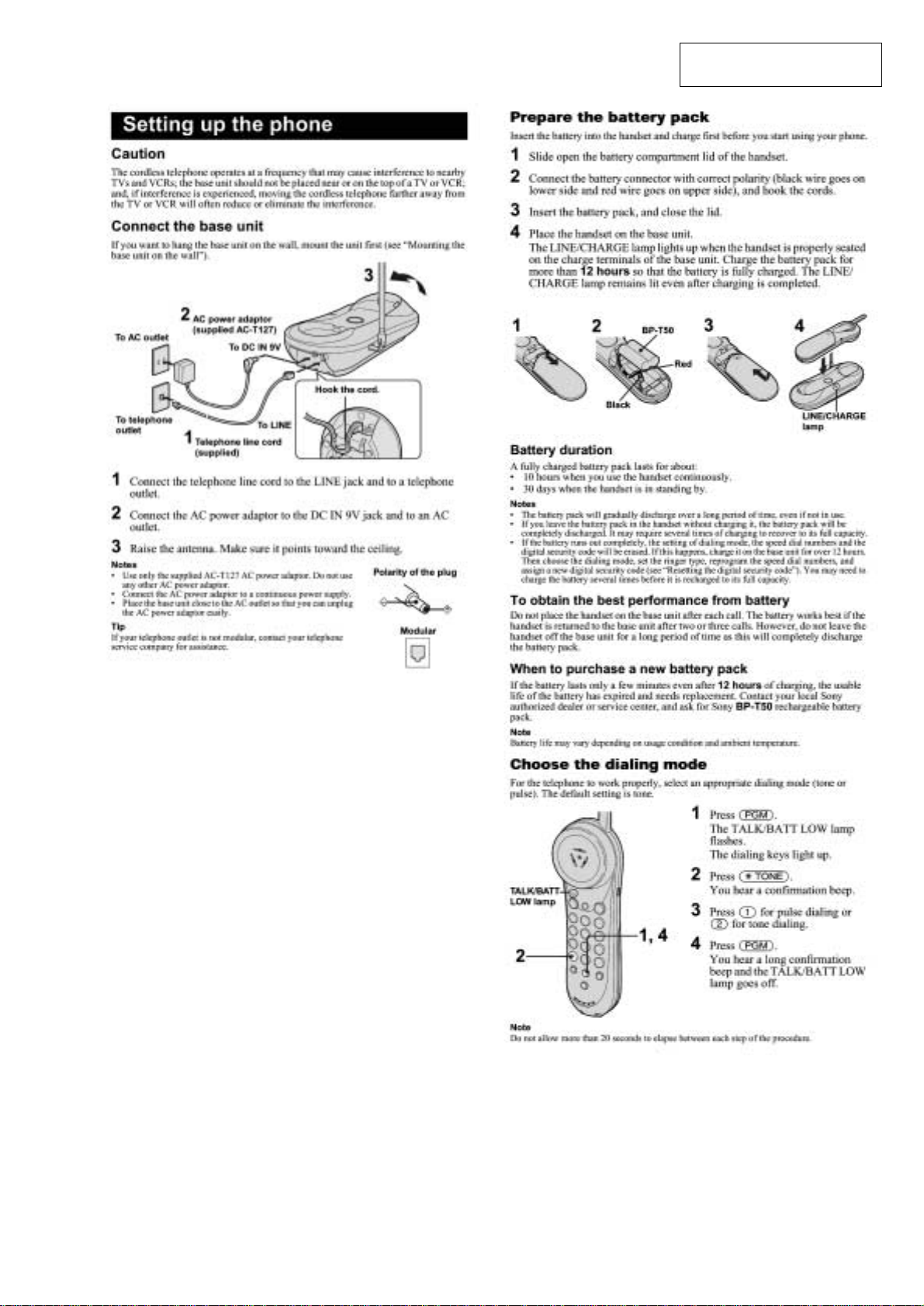
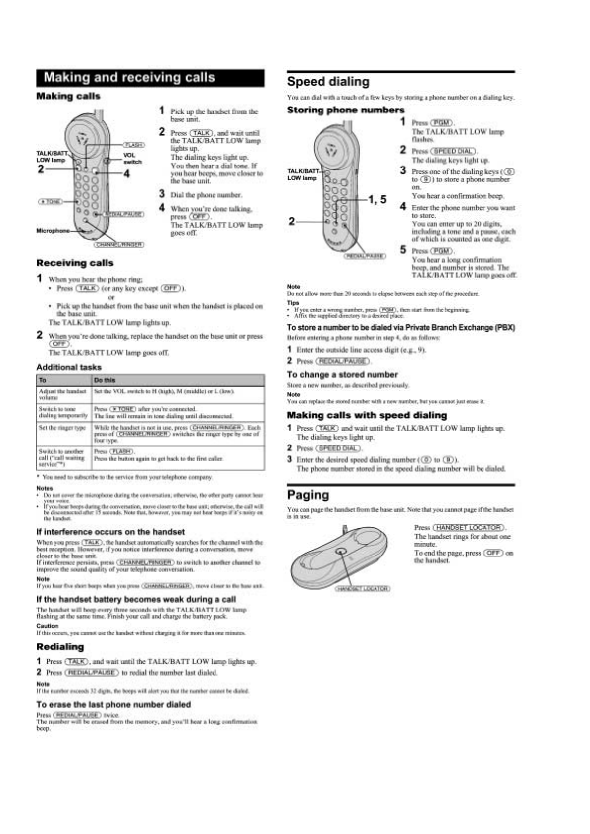
Setting up the phone .......................................................... 3
Making and Receiving calls............................................... 4
Speed dialing...................................................................... 4
Paging ................................................................................ 4
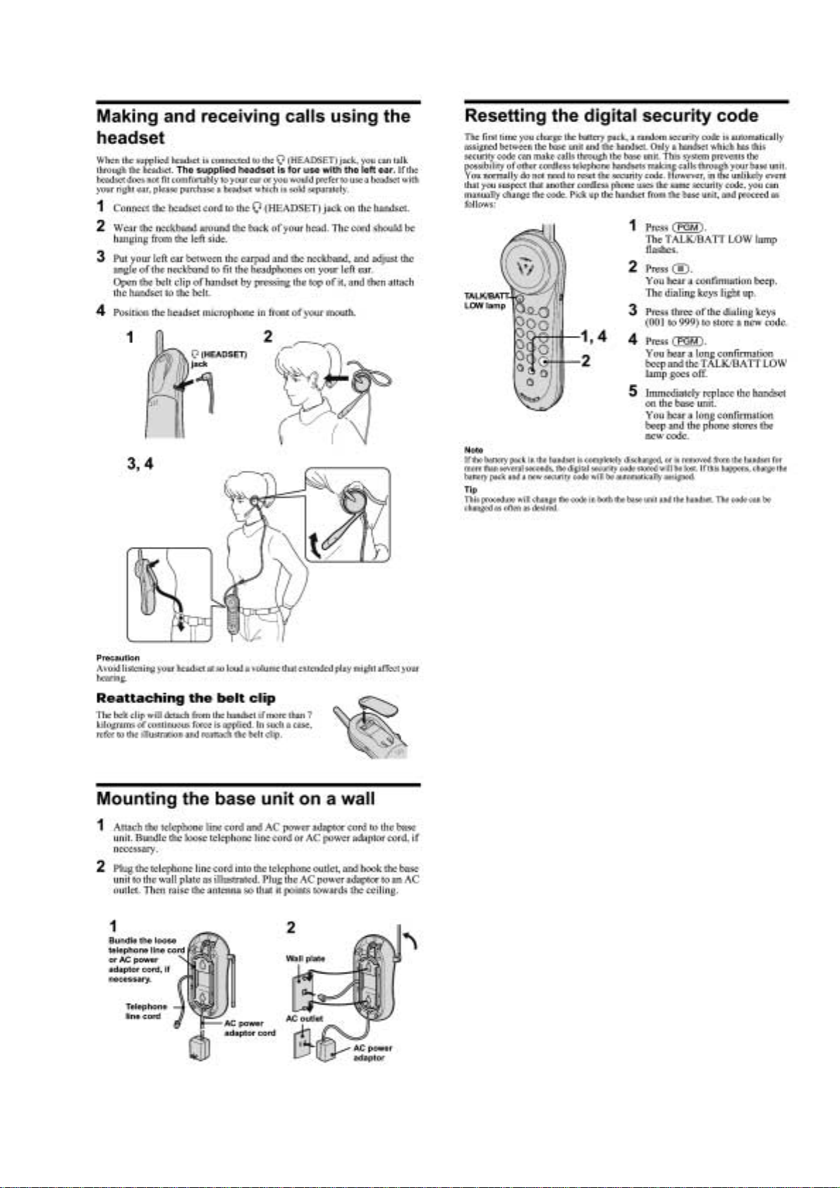
Making and Receiving calls using the
head set (SPP-N1003) ........................................................ 5
Mounting the base unit on a wall ....................................... 5
Resetting the digital security code ..................................... 5
2. DISASSEMBLY
2-1. Cabinet (Upper) .......................................................... 6
2-2. Base Main Board ........................................................ 6
2-3. Cabinet (Rear)............................................................. 7
2-4. Jack Board (SPP-N1003 Only)................................... 7
2-5. Hand Main Board ....................................................... 8
3. TEST MODE................................................................... 9
4. ELECTRICAL ADJUSTMENTS
Base Unit Section..............................................................11
Handset section ................................................................ 13
5. DIAGRAMS
5-1. Explanation of IC Terminals..................................... 15
5-2. Block Diagrams (Base Unit Section)........................ 17
5-3. Block Diagrams (Handset Section) .......................... 19
5-4. Printed Wiring Boards (Base Unit Section).............. 21
5-5. Schematic Diagram (Base Unit Section) .................. 23
5-6. Printed Wiring Boards (Handset Section) ................ 25
5-7. Schematic Diagram (Handset Section)..................... 27
5-8. Printed Wiring Boards (Jack Section)
(SPP-N1003 Only) ................................................... 29
5-7. Schematic Diagram (Jack Section)
(SPP-N1003 Only) ................................................... 30
6. EXPLODED VIEWS
6-1. Base Unit Section ..................................................... 31
6-2. Handset Section ........................................................ 32
6-3. Head set Section (SPP-N1003 Only)........................ 33
NOTE ON BASE MAIN BOARD AND HAND MAIN
BOARD REPAIR
As for base main board and hand main board, there are two type
of “A type” and “B type” by difference of diodes (D401 and
D402) used.
Difference parts list
Base main board
A type B type
D401, D402
BB145B-115 or
HVU-355BTRF
1SV314 (TPH3)
C451 10PF 12PF
C453 4PF 6PF
C454 8PF 7PF
• D401 and D402 using same thing.
Hand main board
A type B type
D401, D402
BB145B-115 or
HVU-355BTRF
1SV314 (TPH3)
C428 10PF 7PF
C450 10PF 12PF
C454 10PF 7PF
L405 15nH 18nH
L409 15nH 18nH
R418 10K 15K
R428 180 220
• D401 and D402 using same thing.
Flexible Circuit Board Repairing
• Keep the temperature of the soldering iron around 270°C during
repairing.
• Do not touch the soldering iron on the same conductor of the
circuit board (within 3 times).
• Be careful not to apply force on the conductor when soldering or
unsoldering.
Notes on chip component replacement
• Never reuse a disconnected chip component.
• Notice that the minus side of a tantalum capacitor may be damaged by heat.
7. ELECTRICAL PARTS LIST.................................... 34
SAFETY-RELATED COMPONENT WARNING!!
COMPONENTS IDENTIFIED BY MARK ! OR DOTTED LINE WITH
MARK !ON THE SCHEMATIC DIAGRAMS AND IN THE PARTS
LIST ARE CRITICAL TO SAFE OPERATION.
REPLACE THESE COMPONENTS WITH SONY PARTS WHOSE
PART NUMBERS APPEAR AS SHOWN IN THIS MANUAL OR IN
SUPPLEMENTS PUBLISHED BY SONY.
ATTENTION AU COMPOSANT AYANT RAPPORT
À LA SÉCURITÉ!
LES COMPOSANTS IDENTIFIÉS P AR UNE MARQUE ! SUR LES
DIAGRAMMES SCHÉMA TIQUES ET LA LISTE DES PIÈCES SONT
CRITIQUES POUR LA SÉCURITÉ DE FONCTIONNEMENT. NE
REMPLACER CES COMPOSANTS QUE PAR DES PIÈCES SONY
DONT LES NUMÉROS SONT DONNÉS DANS CE MANUEL OU
DANS LES SUPPLÉMENTS PUBLIÉS PAR SONY.
– 2 –
SECTION 1
GENERAL
This section is extracted from
instruction manual.
– 3 –
– 4 –
(SPP-N1003)
– 5 –
SECTION 2
)
DISASSEMBLY
r
The equipment can be removed using the following procedure.
Cabinet (upper)Base unit Base main board
Cabinet (rear)Handset Jack board (SPP-N1003 only) Hand main board
Note : Follow the disassembly procedure in the numerical order given.
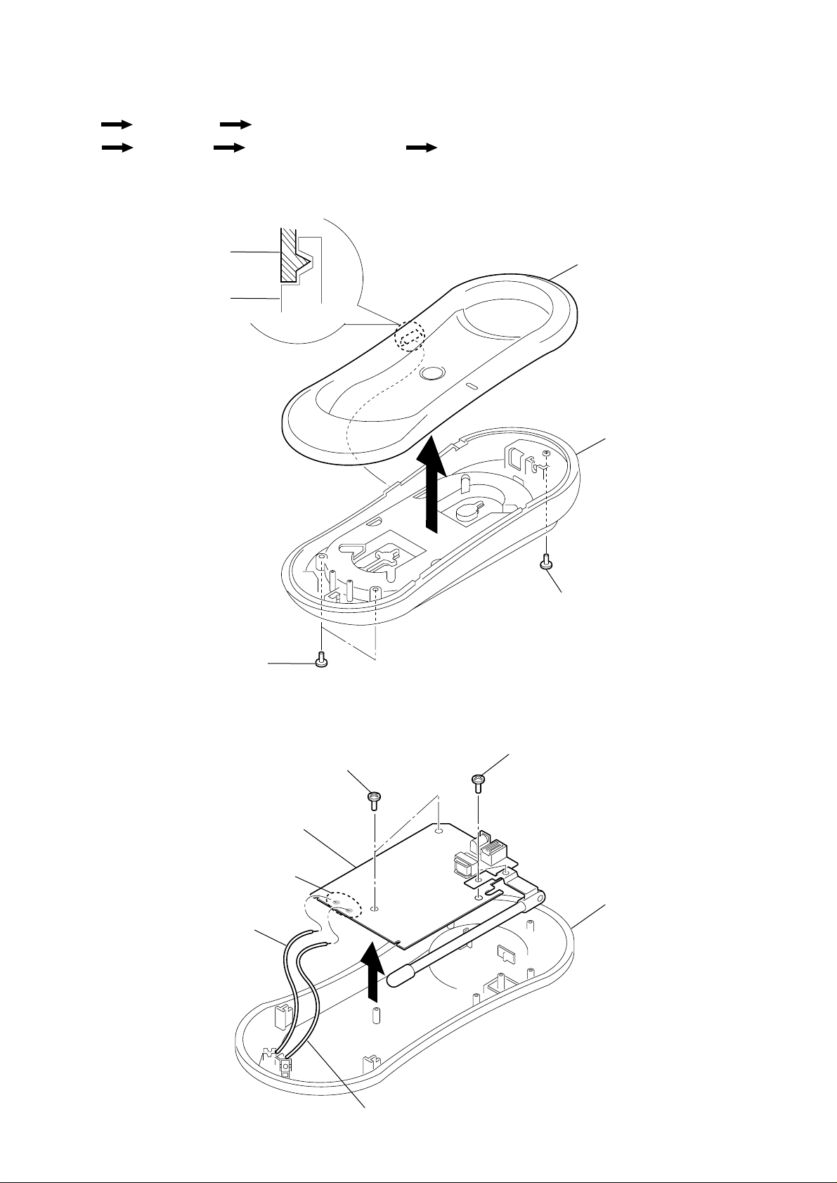
2-1. CABINET (UPPER)
Cabinet (upper)
Cabinet (lower)
2
Claw
3
Cabinet (upper)
Cabinet (lower
1
Screw (+P 3x8)
1
Screws (+P 3x8)
2-2. BASE MAIN BOARD
2
Screws (+BTP 2.6x8)
Base main board
3
Remove solder
White
4
1
Screws (+BTP 2.6x8)
Cabinet (lower)
Red
– 6 –
2-3. CABINET (REAR)
e
Cabinet (rear)
Cabinet (front)
Cabinet (rear)
Claws
3
1
3
Claws
4
Cabinet (rear)
Cabinet (front)
2
Screws (+BTP 2.6x12)
Lid, battery cas
Cabinet (front)
2-4. JACK BOARD (SPP-N1003 ONLY)
Cabinet (front)
1
Screws
(+BTP 2.6x8)
3
CN801
Jack board
Cabinet (rear)
– 7 –
2
Claws
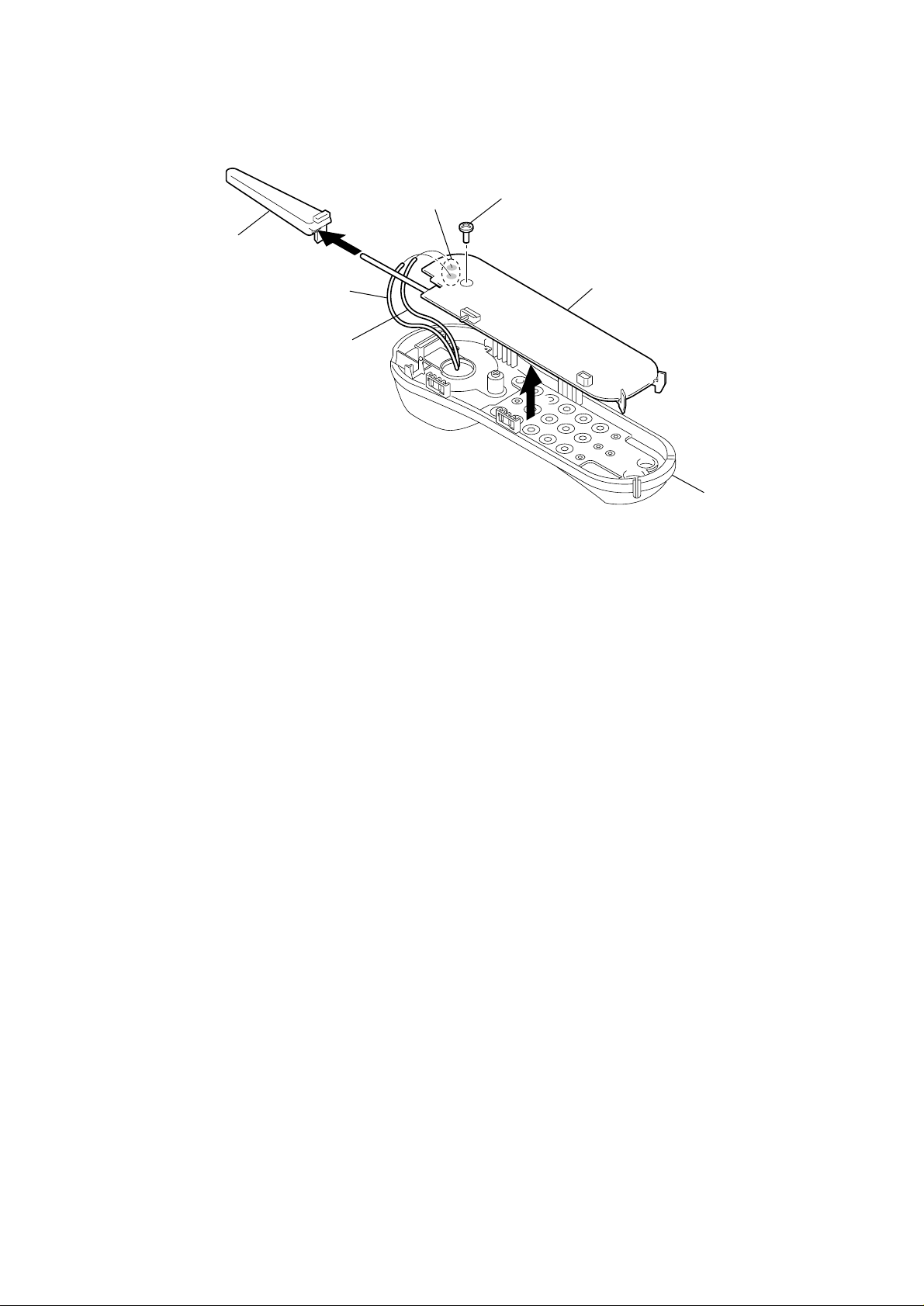
2-5. HAND MAIN BOARD
Cover (antenna)
1
Remove solder
4
Red
Black
2
Screws (+BTP 2.6x10)
Hand main board
3
Cabinet (front)
– 8 –
SECTION 3
TEST MODE
BASE UNIT MANUAL TEST MODE
1 Base Unit Manual Test Mode Startup Procedure
1. Turn on the power while holding down the HANDSET LOCATOR key, then perform the following steps within 10 seconds.
2. Set Charge ON (Place the handset on the base unit).
3. Set Charge OFF (Remove the handset).
4. Set Charge ON.
5. Set Charge OFF.
6. Release the HANDSET LOCATOR key.
7. Press the HANDSET LOCATOR key twice. (Transmit power
turns on. Default Channel = 1)
2 Changing Channels
The current channel number increases by 1 each time the HANDSET LOCATOR key is pressed after shifting to test mode. Channel 1 is the default channel.
After being in CH32, pressing the HANDSET LOCATOR key
returns to CH1.
CHANNEL MAP
Handset TX Handset RX
CH Base RX Base RX
(MHz) (MHz)
1 902,200 924,900
2 902,300 925,000
3 902,400 925,100
4 902,500 925,200
5 902,600 925,300
6 902,700 925,400
7 902,800 925,500
8 902,900 925,600
9 903,000 925,700
10 903,100 925,800
11 903,200 925,900
12 903,300 926,000
13 903,400 926,100
14 903,500 926,200
15 903,600 926,300
16 903,700 926,400
17 903,800 926,500
18 903,900 926,600
19 904,000 926,700
20 904,100 926,800
21 904,200 926,900
22 904,300 927,000
23 904,400 927,100
24 904,500 927,200
25 904,600 927,300
26 904,700 927,400
27 904,800 927,500
28 904,900 927,600
29 905,000 927,700
30 905,100 927,800
31 902,000 924,700
32 905,300 928,000
HANDSET MANUAL TEST MODE
1 Handset Manual Test Mode Startup Procedure
1. Hold down the T ALK key for at least 2 seconds while pressing
the 0 and 1 keys in idle.
2. The call bell rings for half a second (500 msec) as test mode
starts up.
(Status after startup is called Test Idle mode).
2 Detecting Electromagnetic Intensity (RSSI)
After test mode starts up, electromagnetic intensity (RSSI) is measured. The TALK led lights up if the electromagnetic intensity
exceeds a certain level (Level indicating RF during normal receive scanning).
3 Key operation in Test Idle Mode
The following keys function as shown during test idle mode.
KEY DESCRIPTION REMARKS
CHANNEL Increments channel by +1 each
timepressed. Pressing
CHANNEL after being in CH32
returns to CH1.
1 Transmit power on Default TX
4 Transmit power off = off
2 Receive mute off Default RX
5 Receive mute on mute = off
3 RSSI sensitivity setting HIGH Default level
6 RSSI sensitivity setting HIGH = High
SPEED
DIAL Default
REDIAL/
PAUSE
FLASH selector (HIGH t MID t
OFF Quit test mode
Using the following keys in test idle mode shifts operation to a
specific mode. Shifting to these modes disables the key operations
in the above table. Pressing the OFF key returns to test idle mode.
KEY DESCRIPTION REMARKS
7
8
9
(STAR) Shifts to destination check mode
# (POUND)
Half-mute off
Half-mute on
Telephone receiver volume
NORMAL t HIGH)
Power saving measurement
mode 1 (in call status)
Power saving measurement
mode 2 (in call receive)
Power saving measurement
mode 3 (in standby)
Shifts to battery voltage test
mode
Default CH=1
HMUTE = off
Default volume
= High
– 9 –
4 Power Saving Measurement Mode
To enter power saving measurement mode, press one of the 7, 8,
9 keys while in test idle mode. Pressing the OFF key after entering power saving measurement mode returns the operation to test
idle mode.
KEY DESCRIPTION
7 Shifts to same status as during a call ON ON
Shifts to same status as in call
8
receive. (transmit off)
Shifts to same status as during
9
standby. (transmit/receive off)
5 Destination Check
To enter destination check mode, press the (star) key in test
idle mode. Pressing the OFF key after entering destination check
mode returns the operation to test idle mode.
Mexican model ON ON
Cenreal & South American model OFF OFF
US, Canadian model BLINK OFF
6 Battery Voltage Test Mode
To enter battery voltage test mode, press the # (pound) key in test
idle mode. In this mode, the T ALK LED lights up when the battery
is low.
Pressing the OFF key after entering battery voltage test mode returns the operation to test idle mode.
Battery low TALK LED on
Battery OK TALK LED off
TALK Lighted
LED Key
OFF OFF
OFF OFF
Battery Lighted Key
7 Data Reset
Recharging the handset while in test idle mode, resets the security code (handset ID), quick-dial & redial information, and different settings.
– 10 –

SECTION 4
ELECTRICAL ADJUSTMENTS
BASE UNIT
BASE UNIT TX ADJUSTMENT
1. Transmit Mode Setting Procedure
1. Start up the test mode according to the “Manual Test Mode
Startup Procedure”. (See page 9)
2. Press the PAGE key (HANDSET LOCATOR) and make the
channel settings. (Default CH=1)
3. Ground TP201 (RING DET).
2. TX Frequency Adjustment
Connect the frequency counter to TP406 (ANT), and adjust the
TX frequency by turning CT501.
Standard value : Transmit frequency ± 1kHz
BASE UNIT RX ADJUSTMENT
1. Transmit Mode Setting Procedure
1. Start up the test mode according to the Manual Test Mode
Startup Procedure. (See page 9)
2. Press the PAGE key (HANDSET LOCATOR) and make the
channel settings. (Default CH=1)
2. RX Carrier Adjustment
1. Start up the test mode according to the Manual Test Mode.
2. Set the signal generator to Setting1 and the audio analyzer to
DIST. mode. Turn T401 and adjust so that the output level is
near maximum and the DC voltage of TP404 is 1.1 volts.
Check that the output level on the audio analyzer is within the
standard value.
Standard value: 210 to 410 mV.
Also check on an oscilloscope that there is no waveform distortion on the demodulated signal.
3. RSSI (H) Sensitivity Adjustment
Set the signal generator to Setting 2 and adjust R V401 so that the
RSSI output voltage is 220 mV.
SIGNAL GENERATOR SETTINGS
Setting Frequency RF Output Modulation Modulation
No. (MHz) (dBµ VEMF) (kHzINT) Factor
Setting 1 60 1 20kHz
Setting 2 no signal - -
– 11 –
t
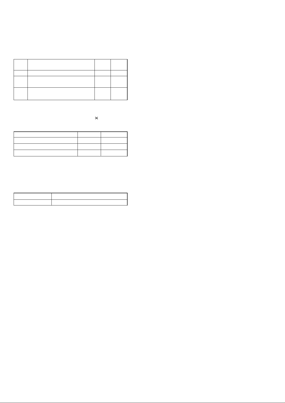
Connection and adjustment location :
FM RF signal
generator
TP406
(ANT)
TP407
(RF GND)
TP407
oscilloscope
(RF GND)
TP406
(ANT)
BASE MAIN BOARD (SIDE B)
TP101
(VDD)
TP406
(ANT)
TP102
(GND)
frequency counter
digital
voltmeter
TP407
(RF GND)
TP406
(ANT)
TP407
(RF GND)
TP404
(AF OUT)
TP404
(AF OUT)
BASE MAIN BOARD (SIDE A)
TP401
(RSSI)
digital
voltmeter
TP401
(RSSI)
CT501: TX Frequency adjustmernt
– 12 –
IC401
audio analyzer
IC401
t;
IC401
rl
T401 : RX Carrier adjustment
RV401 :
RSSI (H) Sensitivity adjustmen

HANDSET
HANDSET TX ADJUSTMENT
1 Initial Settings
1. Start up test mode according to the “Manual Test Mode Startup
Procedure”. (See page 9)
2. Press the CHANNEL key and make the channel settings. (Default CH=1)
3. Press the 1 key and set TX to ON.
2. TX Frequency Adjustment
Connect the frequency counter to TP401 (ANT), and adjust the
TX frequency by turning CT501.
Standard value: Transmit frequency ±1 kHz
HANDSET RX CHECK
1 Initial Settings
1. Start up test mode according to the “Manual T est Mode Startup
Procedure”. (See page 9)
2. Press the CHANNEL key and make the channel settings. (Default CH=1)
2. RX Carrier Adjustment
Set the signal generator to Setting1 and set the audio analyzer to
AC LEVEL mode. Turn T401 and adjust so that the output level
is near maximum and so the DC voltage of adjust TP403 (AF
OUT) is 1.1 V.
Check that the output level on the audio analyzer is within the
standard value.
Standard value: 190 to 320 mV.
Also check on an oscilloscope that there is no waveform distortion on the demodulated signal.
SIGNAL GENERATOR SETTINGS
Setting Frequency RF Output Modulation Modulation
No. (MHz) (dBµ VEMF) (kHzINT) Factor
Setting 1 60 1 20kHz
Setting 2 no signal - -
– 13 –
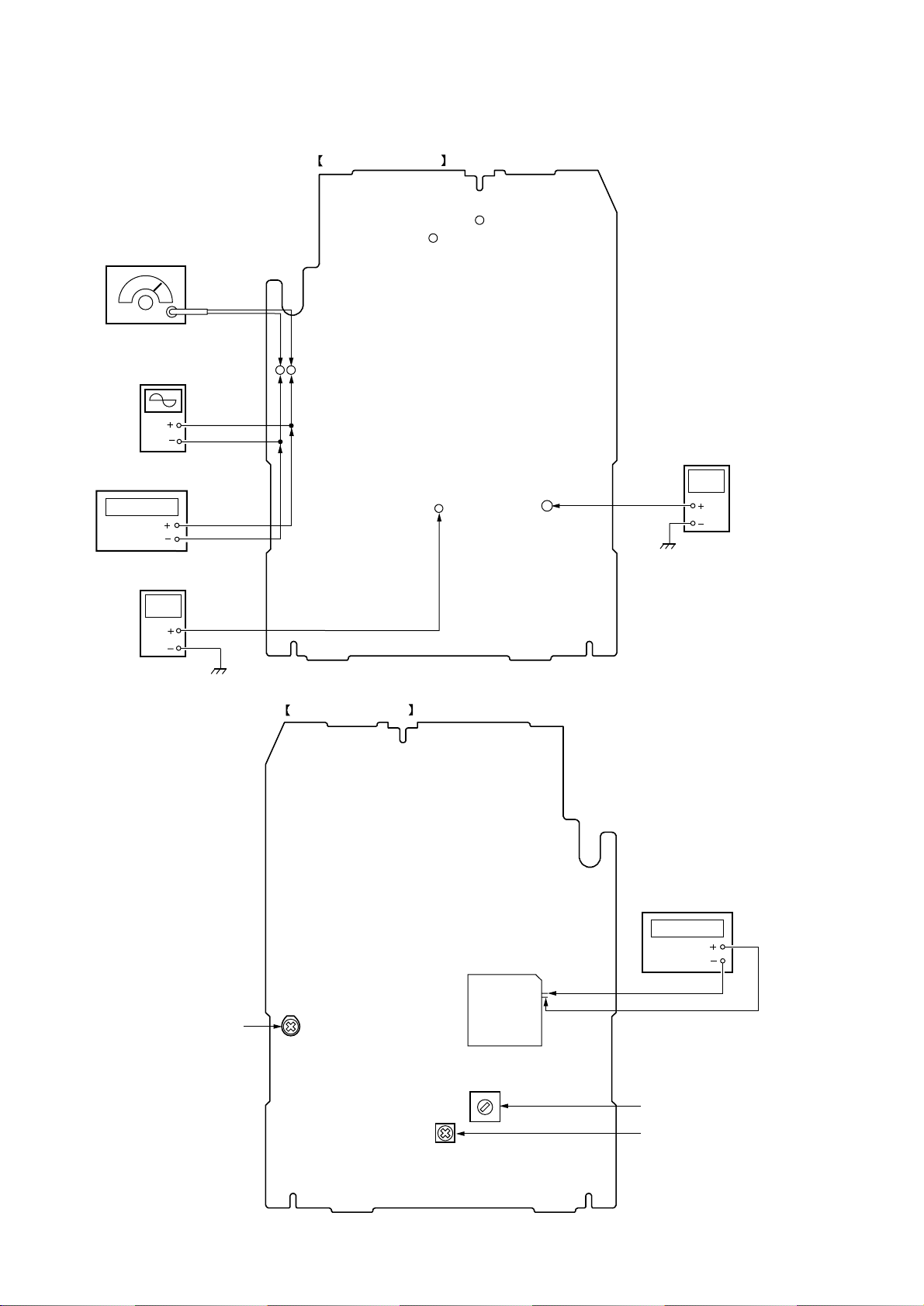
r
Connection and adjustment location :
FM RF signal
generator
oscilloscope
TP401 (ANT)
TP402 (RF GND)
HAND MAIN BOARD (SIDE B)
HAND MAIN BOARD (SIDE A)
audio analyzer
TP402
150
TP401
(ANT)
TP409
(SPB)
Ω
TP403
(AF OUT)
TP408
(SPR)
(RF GND)
TP403
TP408 (SPR)
(AF OUT)
TP409 (SPB)
CT501: TX Frequency adjustmernt
TP401
(ANT)
TP402
(RF GND)
digital
voltmeter
frequency counte
T401 :
RX Carrier adjustment
RV401 :
RSSI (H) Sensitivity adjustment
– 14 –

SECTION 5
DIAGRAMS
5-1. EXPLANATION OF IC TERMINALS
IC501 TMP87CH847U-1K06 (BASE UNIT SYSTEM CONTROL)
Pin No. Pin name I/O Description
1 RF CLK O Serial clock output.
2 DTMF LA O Latch output for DTMF IC.
3 QUICK CHG O Quick charge control output.
4 RX DATA I RX data input.
5 –––––––––– — Not used (OPEN).
6 MBR I Pulse Make/Break select input.
7 LINE LED O LED drive output.
8 – 12 DTMF 0 – 4 O Soft DTMF output 0-4.
13 –––––––––– — Not used (OPEN).
14 RESET I Reset input.
15 X IN I System clock input (8MHz).
16 X OUT O System clock output (8MHz).
17 VSS (VASS) — Ground terminal.
18 VAREF — A/D converter reference voltage.
19 –––––––––– — Not used (OPEN).
20 DTMF CD O Disable output for DTMF IC.
21 –––––––––– — Not used (OPEN).
22 DP O Pulse dial output.
23 BATT V I Power voltage input.
24 RSSI I RSSI volatile detection input.
25 PAGE KEY I Key input.
26 TX POWER O TX power control output.
27 –––––––––– — Not used (OPEN).
28 TX VCO O TX VCO power supply control output.
29 –––––––––– — Not used (OPEN).
30 RING DET I Ringer detection input.
31 CHG IN I Battery charge detection input.
32 TX DATA PU O TX data terminal pull-up output.
33 TX DATA O TX data output.
34 TEST IN2 I Test mode input.
35 TEST IN1 I Test mode terminal. “H”: T est mode. “L”: Normal mode
36 TEST OUT O Test mode output.
37 POWER DET I Power failure detection input.
38 –––––––––– — Not used (OPEN).
39 H MUTE O Half mute control output.
40 VDD — power supply terminal.
41 DTMF DATA O DTMF IC control output.
42 DTMF CLK O Clock output for DTMF IC.
43 RF DATA O RF IC control output.
44 RF STB O Strobe output for RF IC control.
– 15 –
 Loading...