

SPP-M920
SERVICE
MANUAL
US Model
SPECIFICATIONS
MICROFILM
CORDLESS TELEP0HONE

TABLE OF CONTENTS
Specifications ........................................................................... 1
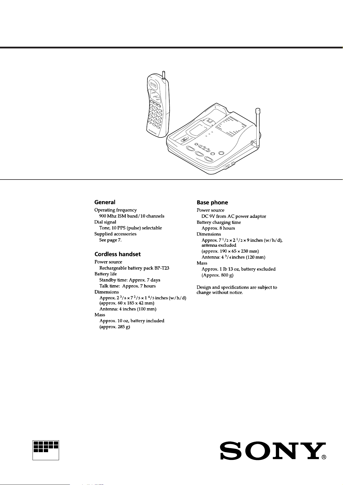
1. GENERAL
Location and Function of Controls .................................... 3
Read this first ..................................................................... 4
Step 1 : Checking the package contents............................. 4
Step 2 : Setting up the base phone ..................................... 4
Step 3 : Preparing the battery pack for the handset ........... 5
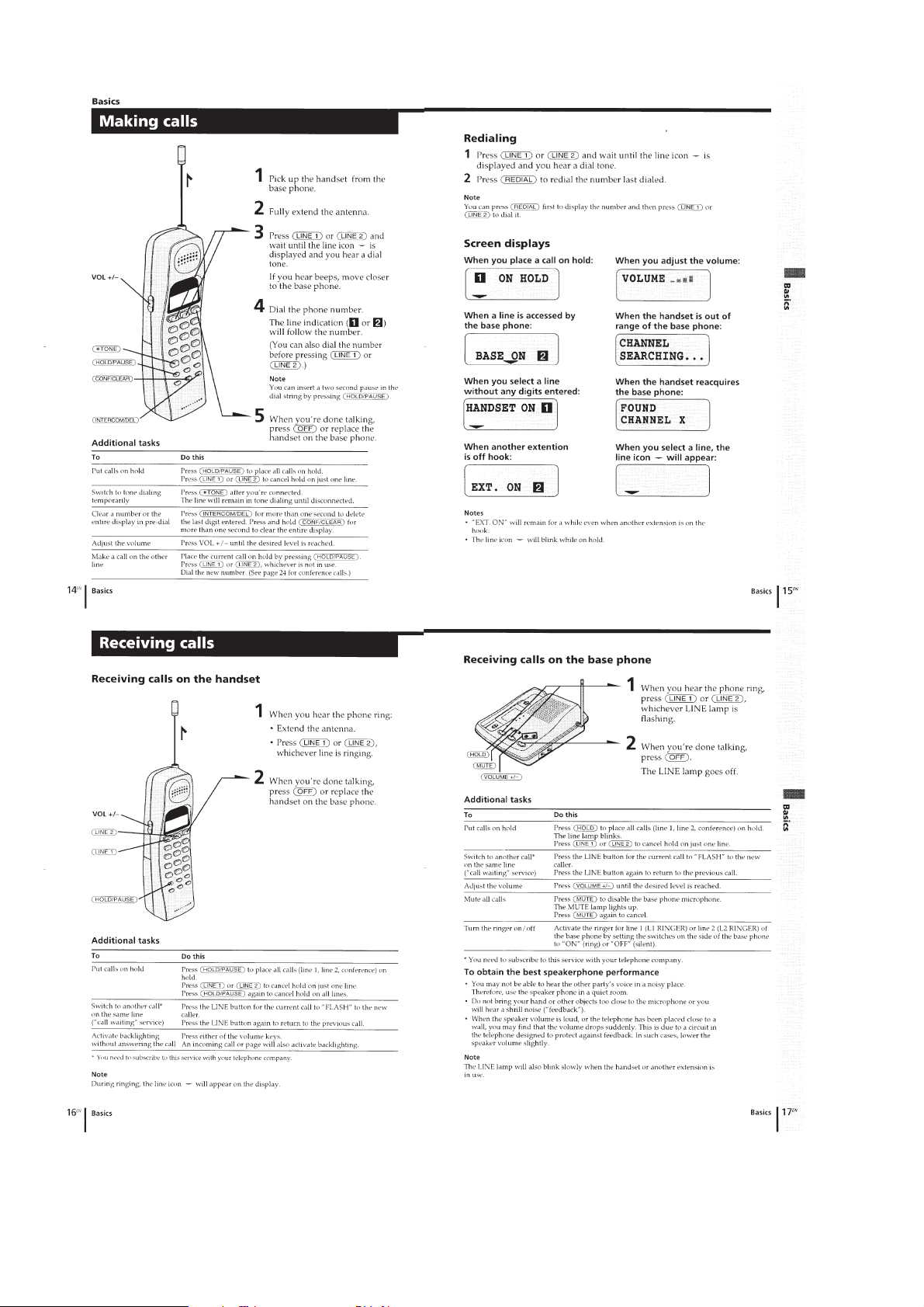
Making calls....................................................................... 5
Receiving calls ................................................................... 6
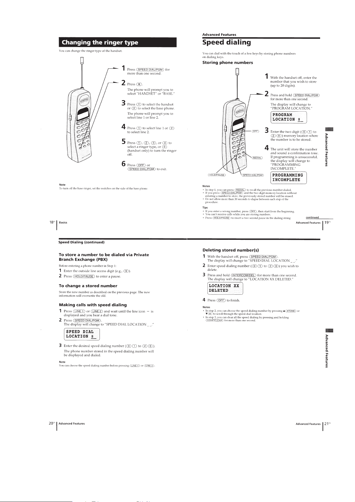
Changing the ringer type.................................................... 7
Speed dialing...................................................................... 7
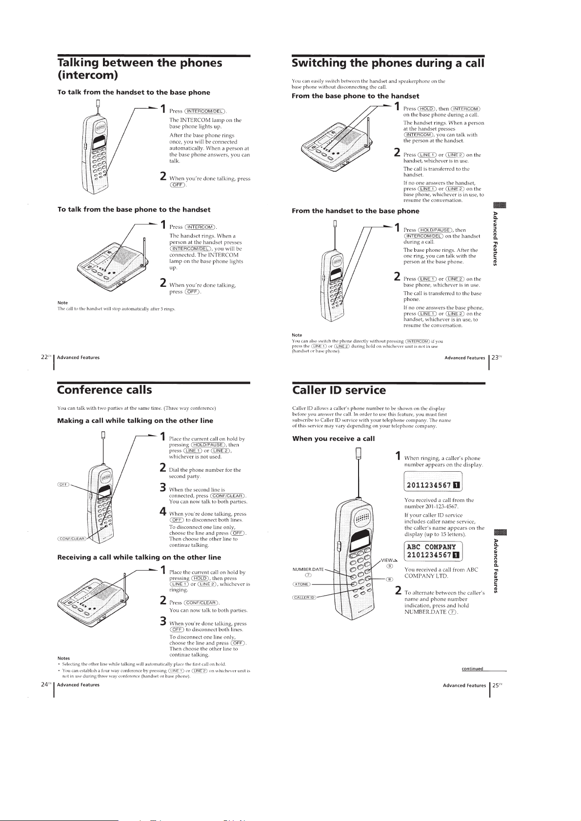
Talking between the phones (intercom) ............................. 8
Switching the phones durig a call ...................................... 8
Conference calls................................................................. 8
Caller ID service ................................................................ 8
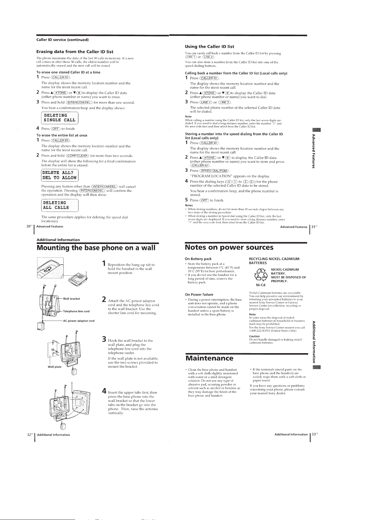
Mounting the base phone on a wall ................................. 10
Notes on power sources ................................................... 10
Maintenance ..................................................................... 10
2. DISASSEMBLY
2-1. Battery Pack Removal ...............................................11
2-2. Hand Cabinet (Rear) Removal ..................................11
2-3. Antenna Removal ..................................................... 12
2-4. Hand Main Board Removal ...................................... 12
3. CIRCUIT OPERATION................................................. 13
4. TEST MODE .................................................................. 19
5. ADJUSTMENTS
5-1. Base Unit Section ..................................................... 22
5-2. Handset Section ........................................................ 24
6. DIAGRAMS
6-1. Explanation of IC Terminals..................................... 26
6-2. Block Diagrams ........................................................ 29
6-3. Printed Wiring Boards (Base Key Section) .............. 35
6-4. Schematic Diagram (Base Key Section) .................. 37
6-5. Schematic Diagram (Base Unit Section) .................. 42
6-6. Printed Wiring Boards (Base Unit Section).............. 47
6-7. Printed Wiring Boards (Handset Section) ................ 52
6-8. Schematic Diagram (Handset Section)..................... 55
7. EXPLODED VIEWS
7-1. Base Unit Section ..................................................... 58
7-2. Handset Section ........................................................ 59
8. ELECTRICAL PARTS LIST ........................................ 60
Flexible Circuit Board Repairing
• Keep the temperature of the soldering iron around 270°C during
repairing.
• Do not touch the soldering iron on the same conductor of the
circuit board (within 3 times).
• Be careful not to apply force on the conductor when soldering or
unsoldering.
Notes on chip component replacement
• Never reuse a disconnected chip component.
• Notice that the minus side of a tantalum capacitor may be damaged by heat.
SAFETY-RELATED COMPONENT WARNING!!
COMPONENTS IDENTIFIED BY MARK ! OR DOTTED LINE WITH
MARK ! ON THE SCHEMATIC DIAGRAMS AND IN THE PARTS
LIST ARE CRITICAL TO SAFE OPERATION.
REPLACE THESE COMPONENTS WITH SONY PARTS WHOSE
PART NUMBERS APPEAR AS SHOWN IN THIS MANUAL OR IN
SUPPLEMENTS PUBLISHED BY SONY.
Notes when repairing/replacing the microcomputer
(Base Unit : IC8, Handset : IC11)
The microcomputer for this equipment initial used an externally
installed ROM version but incorporation of internal software (in-
ternal ROM version) led to elimination of the externally installed
ROM version.
The internal ROM version is available as a service part.
When replacing or servicing this part, the following parts must
also be replaced along with it. (only when set with the external
installed ROM version).
1. HANDSET
IC3, 4 ; Deleted (These were never available as service) parts.
R81 (10k) Deleted
R79 (10k) Added
2. BASE UNIT
IC12, 13 ; Deleted (These were never available as service) parts.
R140 (10k) Deleted
R138 (10k) Added
– 2 –
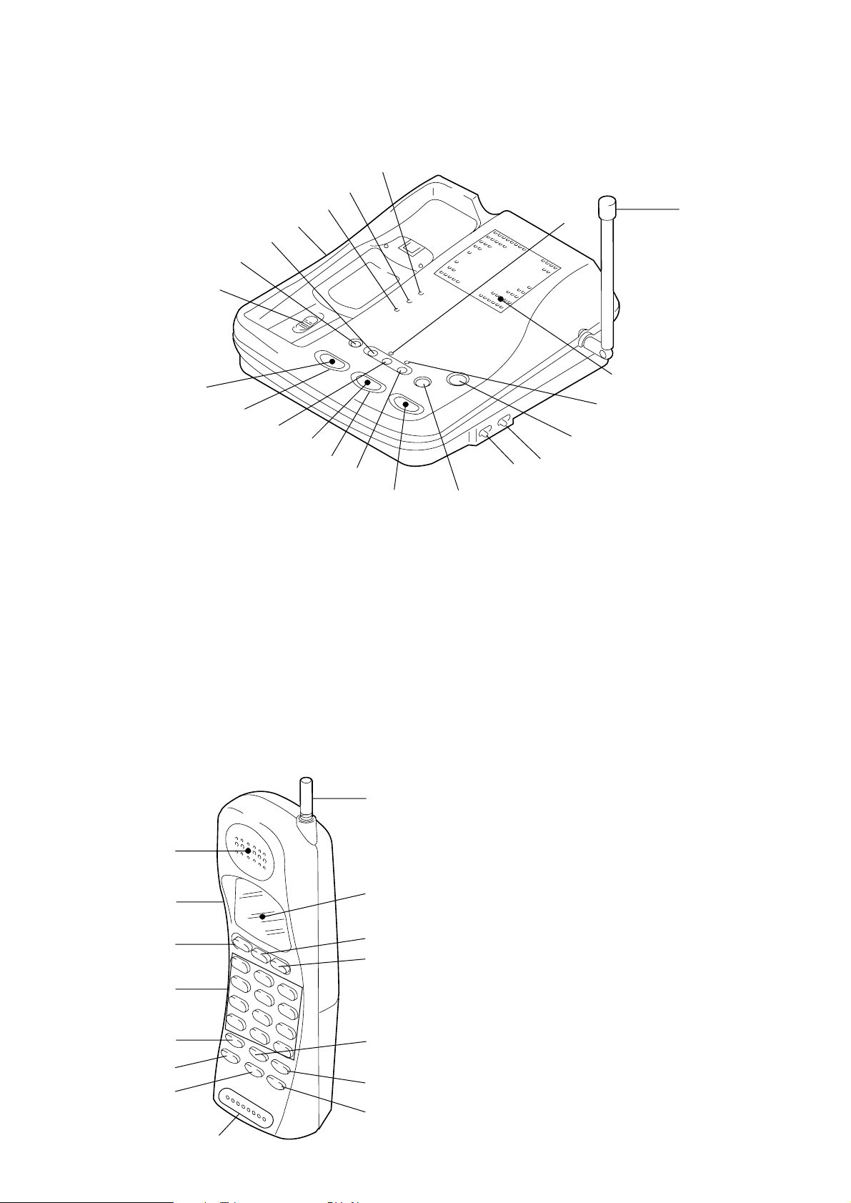
LOCATION AND FUNCTION OF CONTROLS
BASE UNIT
!§
!¶
!•
!ª
@º
@¡
@™
SECTION 1
GENERAL
!∞
!¢
HANDSET
1
2
3
4
1 LINE 1 lamp
2 LINE 1/FLASH button
3 MUTE button
4 LINE 2 lamp
5 LINE 2/FLASH button
6 INTERCOM button
7 OFF button
8 VOLUME – button
9 L1 RINGER ON/OFF button
!º L2 RINGER ON/OFF button
!¡ VOLUME + button
5
6
7
!¡
!º
9
8
!™ INTERCOM lamp
!£ Speaker
!¢ Antenna
!∞ MUTE lamp
!§ POWER lamp
!¶ CHARGE lamp
!• SPARE BATTERY lamp
!ª DIAL MODE (PULSE/TONE)
@º HOLD button
@¡ CONF button
@™ OPEN c (Spare Battery) knob
!£
!™
1
2
3
4
5
6
7
8
!∞
!¢
!£
!™
!¡
!º
9
1 Speaker
2 VOL (Volume) +/– switch
3 LINE 1/FLASH button
4 Dialing keys
5 HOLD/PAUSE button
6 SPEED DIAL/PGM button
7 CONF/CLEAR button
8 Microphone
9 INTERCOM/DEL button
!º REDIAL button
!¡ CALLER ID button
!™ OFF button
!£ LINE 2/FLASH button
!¢ LCD panel
!∞ Antenna
– 3 –
This section is extracted from
instruction manual.
– 4 –
– 5 –
– 6 –
– 7 –
– 8 –
– 9 –
– 10 –
SECTION 2
)
DISASSEMBLY
Note : Follow the disassembly procedure in the numerical order given.
2-1. BATTERY PACK REMOVAL
Lid, Battery pack
Battery pack (BP-T23)
2
1
2-2. HAND CABINET (REAR) REMOVAL
1
Screws
(+BTP 3x12)
2
Hand cabinet (Rear)
3
4
Hand cabinet (Front
2
3
– 11 –
)
2-3. ANTENNA REMOVAL
Tube
1
Antenna (ANT1)
2
3
Hand cabinet (Front)
2-4. HAND MAIN BOARD REMOVAL
6
Screw (+P 3x8)
Hand main board
2
8
1
Screws
(+BTP 2x6)
7
3
Screw (+BTP 3x12)
Holder, Antenna
5
Screw (+BTP 3x12)
4
Screws (+P 2x8)
Switch, Rubber key (VOL)
Hand main cabinet (Front
– 12 –

SECTION 3
CIRCUIT OPERATION
RF SECTION OVERVIEW
1.0 Introduction
The basic function of the base and handset RF sections is to provide a full duplex wireless link between the handset and base sections of the
telephone. This is accomplished by setting up two simultaneous communications links between the handset and base sections. The RF
receiver and transmitter circuity essentially provide a link between the microphone and speaker in the handset to the telephone line in base
set. In this way the phone performs exactly as a corded phone, except without the cord.
The frequency at which the handset transmits to the base is centered around 926.55MHz, and the frequency at which the base transmits to the
handset is centered around 903.8MHz. Unlike a normal 46/49MHz cordless phone, which directly modulates audio (voice) onto the RF
carrier, a phone using the Mark 3 module first digtizes the audio signal and then modulates high speed data onto the RF car rier . The data rate
which is modulated onto the RF carrier is 48kbps. On the receiver side the data is extracted and then converted back into the original audio
signal.
It is important to note that the synthesizer/prescaler IC only operates up to 500MHz. The VCO's therefor e oscillate at roughly 450MHz. The
900MHz signals needed for the transmit and receive sections are generated from the second harmonic of the VCO frequencies.
The following section will outline the transmit frequencies used as well as the corresponding LO frequency which is used for the receiver.
This is followed by the Block diagram and a block by block functional description of the modules.
1.1 Frequency Tables
This section outline the RF frequencies and corresponding channel numbers. The handset uses a high side LO while the base uses a low side
LO to down-convert the incoming signal.
1.1.1 Handset
Channel Transmit (MHz) Receive (MHz) RX LO (MHz)
1.1.2 Base Unit
Channel Transmit (MHz) Receive (MHz) RX LO (MHz)
1 925.05 902.3 913.0
2 925.35 902.6 913.3
3 925.65 902.9 913.6
4 925.95 903.2 913.9
5 926.25 903.5 914.2
6 926.55 903.8 914.5
7 926.85 904.1 914.8
8 927.15 904.4 915.1
9 927.45 904.7 915.4
10 927.75 905.0 915.7
1 902.3 925.05 914.35
2 902.6 925.35 914.65
3 902.9 925.65 914.95
4 903.2 925.95 915.25
5 903.5 926.25 915.55
6 903.8 926.55 915.85
7 904.1 926.85 916.15
8 904.4 927.15 916.45
9 904.7 927.45 916.75
10 905.0 927.75 917.05
– 13 –
1.2 Block diagram
P
Both the handset and base RF sections follow the same block diagram shown below with only minor changes to incorporate the different
transmit and receive frequencies.
2 POLE CERAMIC
2 POLE CERAMIC
Ist RX AMP SAW FILTER 2nd RX AMP MIXER 10.7MHz CERAMIC IF AMP
V-Tune
LOW PASS
FILTER
TX OP AMP
TX DATA
Fin
Fin
V-Tune
DUAL PRESCALER
SYNTHESIZER
10.7MHz CERAMIC
MC10156
DEMODULATOR
RX LO
4.57MHz
3.2MHz REFERENCE
3 LINE DATA BUS
DATA O/
Figure 1. RF Section Block Diagram
As can be seen by the block diagram, there are several important input/output signals which are necessary for operation of the RF section
(this does not include the separate supply lines for both TX and RX sections). An 18.25MHz reference is present for use in the frequency
synthesizers. The accuracy of this 18.25 MHz input will affect the transmit and recei ve frequencies. In order to ensure proper operation of the
RF sections, the 18.25 MHz reference signal must be at least 500mV in amplitude. Also present is the 3-line serial data bus on whic h data is
transferred to the synthesizers to set both the transmit and receive frequencies.
The modulation input allows digital data to be modulated directly onto the TX carrier. The Data output is the demodulated signal after being
filtered and shaped by a comparator. The data is then sent to the AMD ASIC where the original voice signal is reconstructed.
The RF section performs a single down-conversion of the incoming RF signal to 10.7MHz where it is demodulated and sent to the AMD
ASIC. The transmit section directly modulates the carrier.
The following section explains the individual blocks in the RF section in detail. All reference to part numbers correspond to the handset
schematic
RF SECTION DETAILED OPERATION
2-1. Antenna Section
2.1.1 Antenna
The antenna is a device which allows ef fecti v e conversion of energy from air to the RF circuitry. The antennas used are a retractable
1/2 wave with 2.5dB gain relative to an isotropic radiator and a fixed 1/4 wave antenna with roughly 0dB gain relative to an isotropic
radiator. T he duplex er and f ilters w hich follo w the antenna, require a 50Ω match to operate properly . T he antenna is not matched to
50Ω and requires a simple microstrip matching network to achieve this. If a network analyzer is attached to the BFA connector after
disconnecting the duplexer , the antenna match may be measured. In order to achieve a good 50Ω match, one must be careful not to
obstruct the antenna as any object near the antenna will affect its impedance
2.1.2 Duplexer
The Duplexer ensures that the two bandpass filters do not interact with each other. It accomplishes this by making each filter see a
high impedance from the opposite filter in its own passband. This is necessary to ensure that both filter work effectively when
connected together. If the Duplexer were not present, mismatches from one filter would cause the passband of the other to be
distorted and this would degrade performance.
The Duplexer itself is simply composed of two microstrip and discrete filters which shift each filters out of band match to a high
impedance. To ensur e that the Duplexer is operating correctly, the match looking into the filters from the BFA connector may be
measured. To do this it is necessary to remo v e the 0Ω resistor which connects the antenna to the Duplexer. A return loss of approximately 15dB should be measured for both the TX and RX bands.
2.1.3 RX, TX Bandpass Filters
The RX and TX bandpass filters provide two functions. The first is to effectively pass the correct frequencies to the RX and TX
sections. It is important especially for the RX section that these filters have a low insertion loss in order to ensure a low front end
noise figure. These filters are also designed to provide > 25dB rejection for the opposite band. This means that the transmit carrier
will be attenuated by at least 25dB before entering the receive section of the phone. A plot of the low band filter is shown in Figure
2, 3 below.
– 14 –
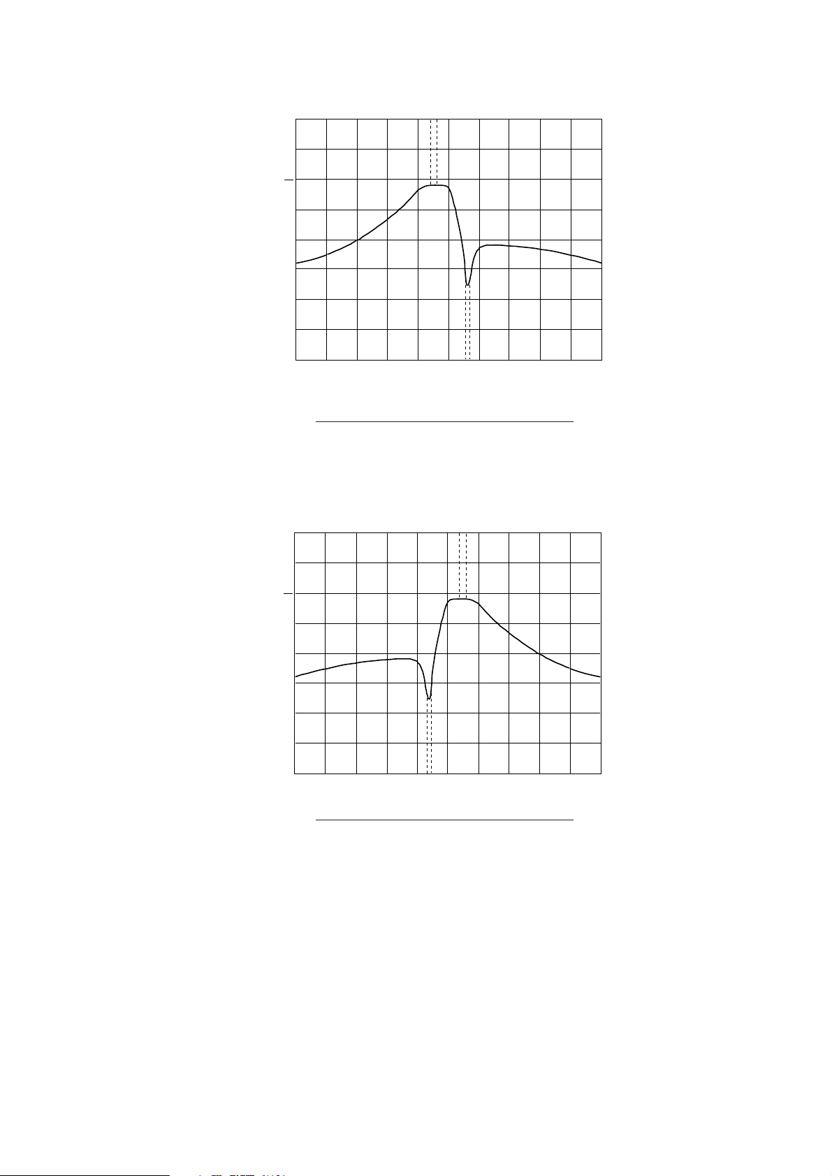
0dB
10dB/div
902-905MHz Passband
815
925-928MHz Reject Band
1015
Figure 2. Low band Ceramic filter response
For this filter the insertion loss is less than 3dB at 902 to 905MHz while the 925 – 928MHz band has > 25dB attenuation. This f ilter is used
for the RX filter in the handset or the TX filter in the base. The high band filter characteristic is shown below. This filter is used for the
handset TX filter and base RX filter.
925-928MHz Passband
0dB
10dB/div
815
902-905MHz Reject Band
Figure 3. High band Ceramic filter response
– 15 –
1015
 Loading...