

Page 1
SPP-ID975/ID976
SERVICE MANUAL
Ver 1.0 1999. 11
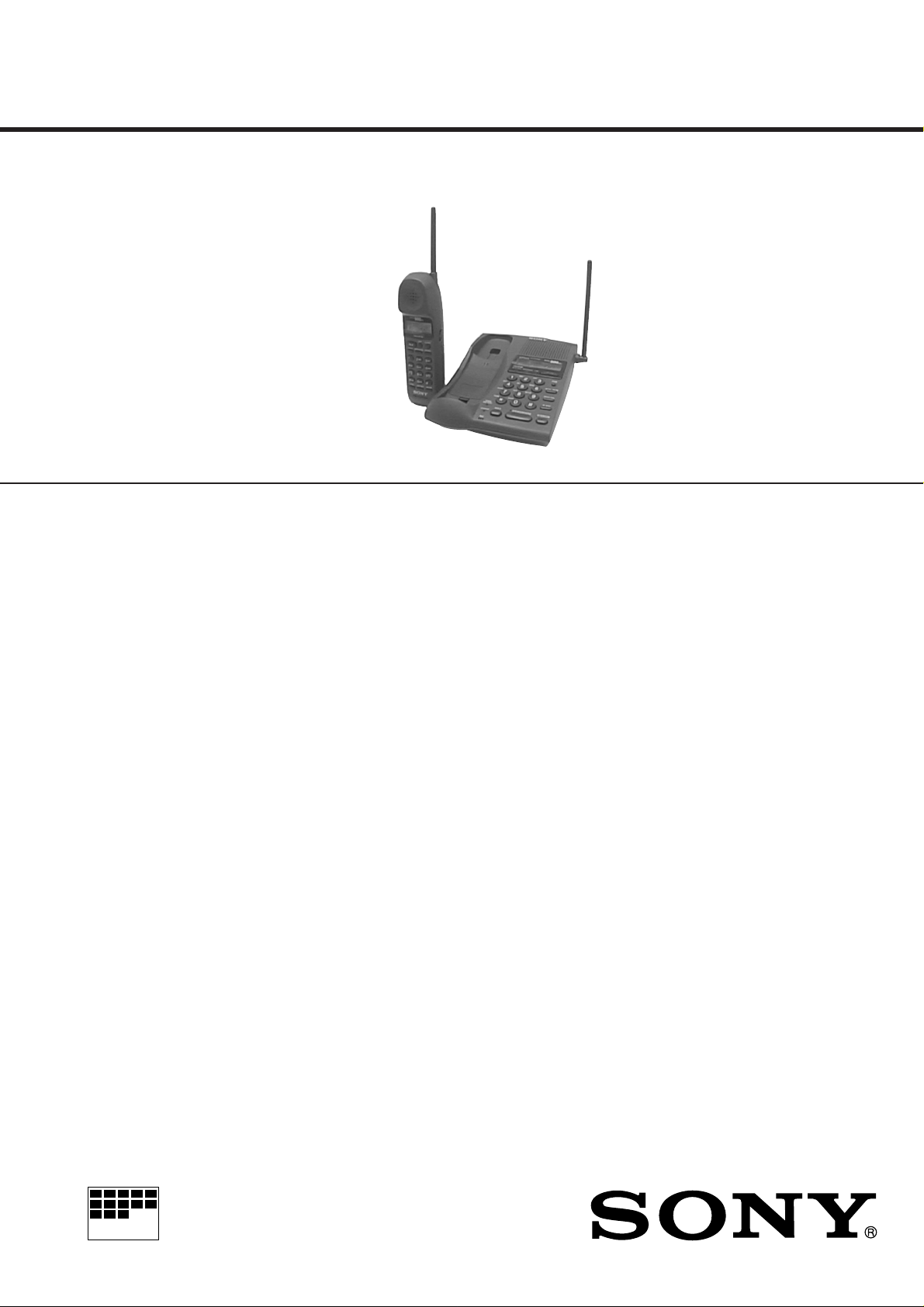
Photo: SPP-ID975
SPECIFICATIONS
General
Frequency band (SPP-ID975)
902 – 928 MHz
Frequency band (SPP-ID976)
923.1 – 927.75 MHz
Base phone : 18 µW
Handset : 73 µW
Operating channel
30 channels
Dial signal
Tone, 10 PPS (pulse) selectable
Supplied accessories
AC power adaptor AC-T122 (1)
Telephone line cords (2)
Wall bracket for base phone (1)
Rechargeable battery pack BP-T23 (1)
Handset
Power source
Rechargeable battery pack BP-T23
Battery charging time
Approx. 12 hours
Battery life
Standby: Approx. 7 days
Talk : Approx. 6 hours
Dimensions
Approx. 58 × 177 × 46 mm (w/h/d),
antenna excluded
(approx. 2 3/8 × 7 × 1 13/16 inches)
Antenna: Approx. 72 mm
(approx. 2 7/8 inches)
Mass
Approx. 270 g
(approx. 9.5 oz), battery included
US Model
SPP-ID975
Canadian Model
SPP-ID976
Base phone
Power source
DC 9V from AC power adaptor
AC-T122
Battery charging time
Approx. 24 hours
Dimensions
Approx. 166 × 63 × 225 mm (w/h/d),
antenna excluded
(approx. 6 5/8 × 2 1/2 × 8 7/8 inches)
Antenna: Approx. 120 mm
(approx. 4 3/4 inches)
Mass
Approx. 595 g
(approx. 1 lb 9 oz), wall bracket excluded
Design and specifications are subject to
change without notice.
Notes on Chip Component Replacement
• Never reuse a disconnected chip component.
• Notice that the minus side of a tantalum capacitor may be dam-
aged by heat.
MICROFILM
CORDLESS TELEPHONE
– 1 –
Page 2
SPP-ID975/ID976
THIS NOTE IS COMMON FOR PRINTED WIRING
BOARDS AND SCHEMATIC DIAGRAMS.
(In addition to this, the necessary note is
printed in each block.)
For schematic diagrams
• All capacitors are in µF unless otherwise noted. pF: µµF
50 WV or less are not indicated except for electrolytics
and tantalums.
• All resistors are in Ω and 1/
specified.
• C : panel designation.
• U : B+ Line.
• Power voltage is dc 9 V and fed with regulated dc power
supply from external power voltage jack. (BASE PHONE)
• Power voltage is dc 12 V and fed with regulated dc power
supply from J1008 with 100 Ω in series. (BASE PHONE)
• Power voltage is dc 3 V and fed with regulated dc power
supply from battery terminal. (HANDSET)
• Voltage is dc with respect to ground under no-signal
condition.
• Voltages are taken with a VOM (Input impedance 10 MΩ).
Voltage variations may be noted due to normal production tolerances.
• Signal path.
N : TX (To Tel Line)
O : RX (From Tel Line)
P : bell
4
W or less unless otherwise
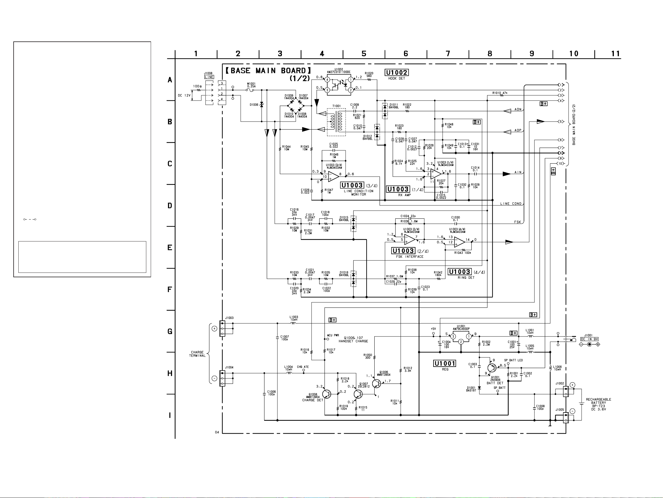
4-3. SCHEMATIC DIAGRAM — BASE MAIN SECTION (1/2) —
(Page 27)
For printed wiring boards
• X : parts extracted from the component side.
• : Carbon pattern.
z
•
• b : Pattern from the side which enables seeing.
Caution:
Pattern face side: Parts on the pattern face side seen from the
(Side B) pattern face are indicated.
Parts face side: Parts on the parts face side seen from the
(Side A) parts face are indicated.
: Through hole.
(The other layer’s patterns are not indicated.)
– 25 – – 26 –
Page 3

4-4. SCHEMATIC DIAGRAM — BASE MAIN SECTION (2/2) — • Refer to page 41 for IC Block Diagrams.
RF UNIT
(BU)
SPP-ID975/ID976
(Page 35)
(Page 26)
– 27 – – 28 –
Page 4

4-7. SCHEMATIC DIAGRAM — BASE KEY SECTION —
SPP-ID975/ID976
(Page 27)
– 35 – – 36 –
Page 5

4-9. SCHEMATIC DIAGRAM — HAND MAIN SECTION — • Refer to page 41 for IC Block Diagrams.
SPP-ID975/ID976
– 39 – – 40 –
Page 6

SECTION 5
EXPLODED VIEWS
• IC Block Diagrams
U1006, 3007 CAT93C86S-LE10
1 8
CS
2
SK
3
DI
4
DO
INSTRUCTION
REGISTER
ADDRESS
REGISTER
DECODER
IOF 1024
(or 2048)
DATA OUT
BUFFER
INSTRUCTION
DECODER, CONTROL
LOGIC AND CLOCK
GENERATORS
EEPROM ARRAY 16384 BIT
& (1024X16) or (2048X8)
READ WRITE AMPS
DATA IN/OUT RESISTER
16 (or 8) BITS
HIGH VOLTAGE
GENERATOR
AND
PROGRAM
TIMER
U3004 MC34118DW
U3001 MC74HC595AF
VCC
NC
7
ORG
6
PARALLEL DATA
16 15 14 13 12 11 10 9
VCC
QA
SERIAL DATA
OUTPUT
A
INPUT
OUTPUT
LATCH
ENABLE
CLOCK
SHIFT
CLOCK
SHIFT REGISTER
RESET
SERIAL DATA
SQH
OUTPUT
NOTE:
• The mechanical parts with no reference
number in the exploded views are not supplied.
• Items marked “*” are not stocked since
they are seldom required for routine service.
Some delay should be anticipated
when ordering these items.
5-1. HANDSET SECTION
• -XX and -X mean standardized parts, so
they may have some difference from the
original one.
• Color Indication of Appearance Parts
Example :
KNOB, BALANCE (WHITE) ... (RED)
R
Parts Color Cabinet’s Color
• Accessories and packing materials are
given in the last of this parts list.
R
ANT1001
16
19
14
9
13
12
9
13
10
11
9
J1003, 1004
LATCH
QC
QD
PARALLEL DATA
OUTPUT
+
_
4321
V in
CF 1
QE
QG
QH
GND
7654321
8
U1005
8
7
6
15
VO1
5
U1003
QB
VSS
5
U3005 MC34119D
VO2
GNDVcc
8 7 6 5
_
+
BIAS
CIRCUIT
CD
CF 2
QF
9
TLO1
TU1
RX0
RX1
RLI2
RLO2
TLO2
TLI2
PU1
GND
28
CPR
27 26 25 24 23 22 21 20 19 18 17 16 15
PLO1
CPT
V8
4
3
J1001, 1002
R
400
BACK GROUND
NOISE MONITER
17
18
R
BIAS
DP-DET
–
RX ATT
BACK GROUND
NOISE MONITER
LEVEL DET
FILTER
–
+
1
FO
2 3 4 5 6 7 8 9 10 11 12 13 14
FI
VR
+ –
CO
Vcc
HTO(+)
R
R
HTO(–)
NTI
+ –
VR
TXO
+
15mV
VR
TX ATT
+
TXI
WCO
LEVEL DET
ATT CONTROL
VR
–
WCI
MUTE
VCL
2
VCC
AGC
Ref. No. Part No. Description Remark
1 3-038-148-01 KEY (HS), RUBBER (ID975)
1 3-038-148-11 KEY (HS), RUBBER (ID976)
2 3-038-075-01 CASE (FR)
3 3-041-211-01 RUBBER, MICROPHONE
4 3-038-081-01 LENS (HS)
5 3-041-520-01 HOLDER (HS), LCD
6 3-041-537-01 RING, CUSHION RECEIVER
7 3-041-212-01 CUSHION, SPEAKER
8 A-3672-875-A RF UNIT (HS)
9 7-685-548-19 SCREW +BTP 3X12 TYPE2 N-S
10 3-038-076-01 CASE (REAR)
11 3-038-083-01 LID (HS), BATTERY CASE
CT
12 4-356-741-21 SCREW, TAPPING (BIND 2X8)
13 4-356-741-11 SCREW, TAPPING (BIND 2X6)
1
LCD1001
Ref. No. Part No. Description Remark
15 3-041-535-01 FELT, RX
* 16 A-3672-876-A HAND MAIN BOARD, COMPLETE (ID975)
* 16 A-3672-897-A HAND MAIN BOARD, COMPLETE (ID976)
17 3-038-084-01 DIFFUSER (HS)
18 3-041-536-01 SHEET
19 3-041-547-01 COVER (HS), HOOK
ANT1001 1-754-103-11 ANTENNA
J1001 3-041-208-01 TERMINAL, CHARGE
J1002 3-041-208-01 TERMINAL, CHARGE
J1003 3-041-210-01 TERMINAL, BATTERY
J1004 3-041-210-01 TERMINAL, BATTERY
LCD1001 1-803-832-11 LCD MODULE
U1003 1-542-260-31 MICROPHONE, ELECTRET CONDENSER
U1005 1-505-593-11 SPEAKER (2.8cm)
14 3-038-085-01 KNOB (HS), VOLUME
– 41 – – 42 –
 Loading...