Sony SPP-A973 Service manual
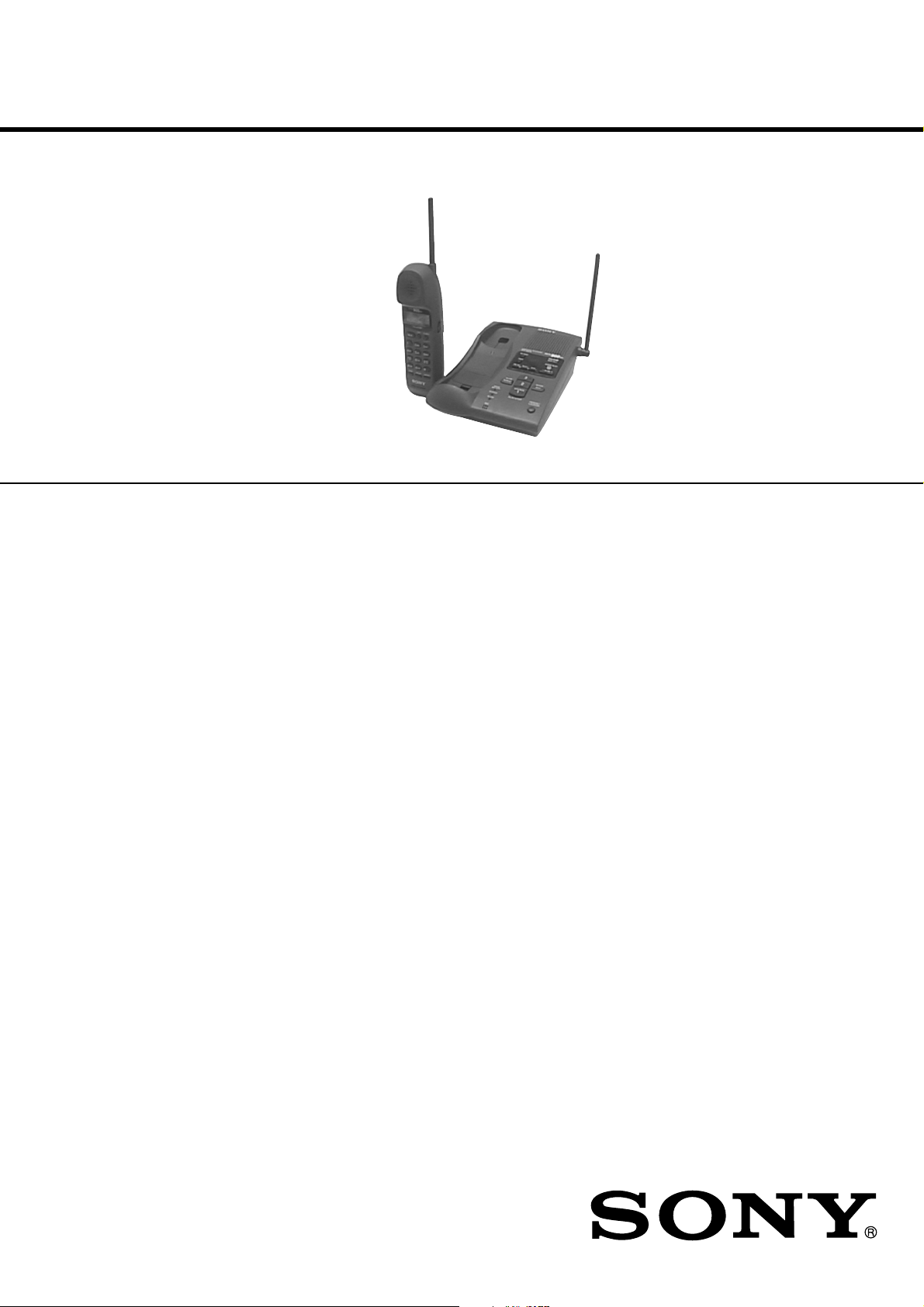
SPP-A973/A974
SERVICE MANUAL
Ver 1.4 2001. 05
Photo: SPP-A973
SPECIFICATIONS
General
Frequency band (SPP-A973)
902 – 928 MHz
Frequency band (SPP-A974)
923.1 – 927.75 MHz
Base unit : 18 µW
Handset : 73 µW
Operating channel
30 channels
Dial signal
Tone, 10 PPS (pulse) selectable
Supplied accessories
AC power adaptor AC-T128 (1)
Telephone line cords (2)
Wall bracket for base phone (1)
Rechargeable battery pack BP-T23 (1)
Handset
Power source
Rechargeable battery pack BP-T23
Battery charging time
Approx. 12 hours
Battery life
Standby: Approx. 7 days
Talk : Approx. 6 hours
Dimensions
Approx. 58 × 177 × 46 mm (w/h/d),
antenna excluded
(approx. 2 3/8 × 7 × 1 13/16 inches)
Antenna: Approx. 72 mm
(approx. 2 7/8 inches)
Mass
Approx. 270 g
(approx. 9.5 oz), battery included
US Model
SPP-A973
Canadian Model
SPP-A974
Base unit
Power source
DC 9 V from AC power adaptor
AC-T128
Battery charging time
Approx. 24 hours
Dimensions
Approx. 160 × 63 × 225 mm (w/h/d),
antenna excluded
(approx. 6 3/8 × 2 1/2 × 8 7/8 inches)
Antenna: Approx. 120 mm
(approx. 4 3/4 inches)
Mass
Approx. 585 g
(approx. 1 lb 5 oz), wall bracket excluded
Answering machine
Maximum recording time
About 15 minutes, using incorporated IC
Greeting message
Up to 90 seconds per each
Incoming and Memo message
Up to 4 minutes per message
Design and specifications are subject to
change without notice.
Notes on Chip Component Replacement
• Never reuse a disconnected chip component.
• Notice that the minus side of a tantalum capacitor may be dam-
aged by heat.
9-927-618-12
2001E0400-1
© 2001. 5
CORDLESS TELEPHONE
Sony Corporation
Personal Audio Company
Shinagawa Tec Service Manual Production Group
– 1 –
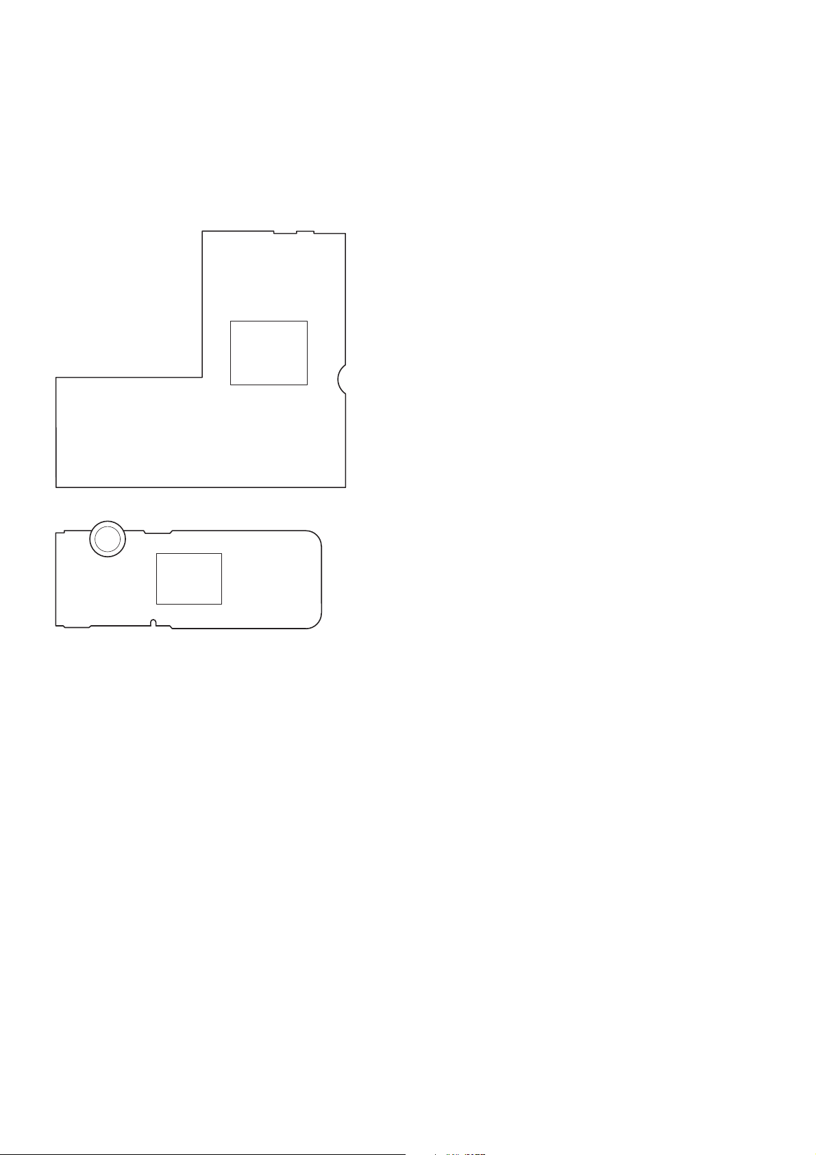
Note for Replacement of the ASIC Board
The ID is written in the ASIC board.
When replacing the ASIC board, the U4001 on BASE MAIN board
and U1001 on HAND MAIN board should be replaced together as
a pair.
Part No. : X-3378-160-1 ASIC ASSY (one assy of two parts)
– BASE MAIN BOARD (SIDE A) –
U4001
TABLE OF CONTENTS
1. GENERAL
Read This First ........................................................................ 3
Checking the Package Contents ..............................................3
Setting Up the Base Unit ......................................................... 3
Preparing the Battery Pack ...................................................... 4
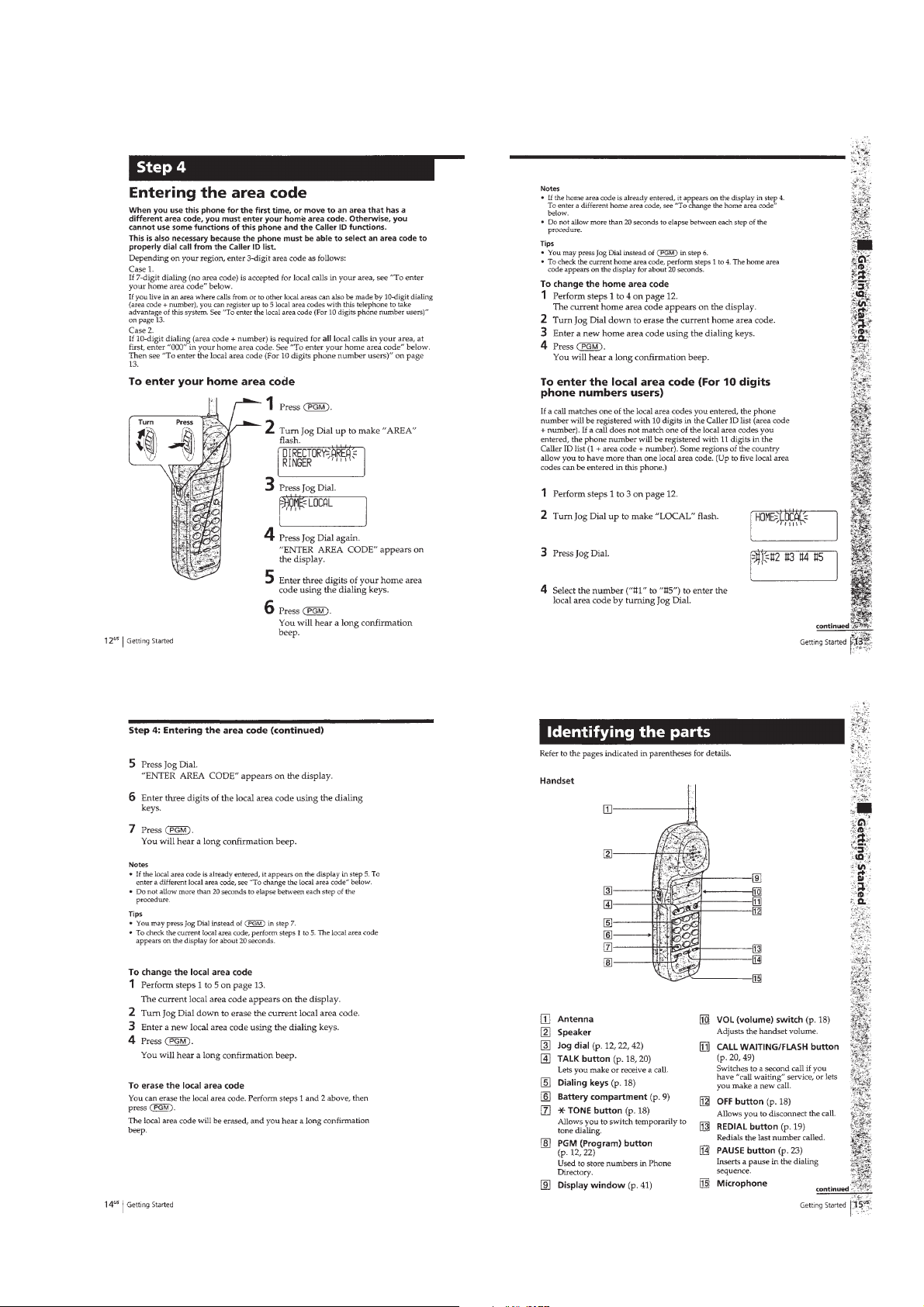
Entering the Area Code ........................................................... 5
Identifying the Parts ................................................................5
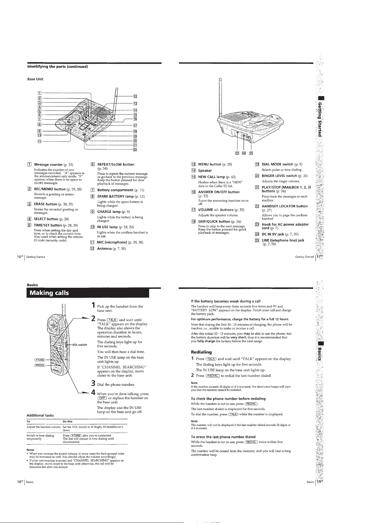
Making Calls ...........................................................................6
Receiving Calls........................................................................ 7
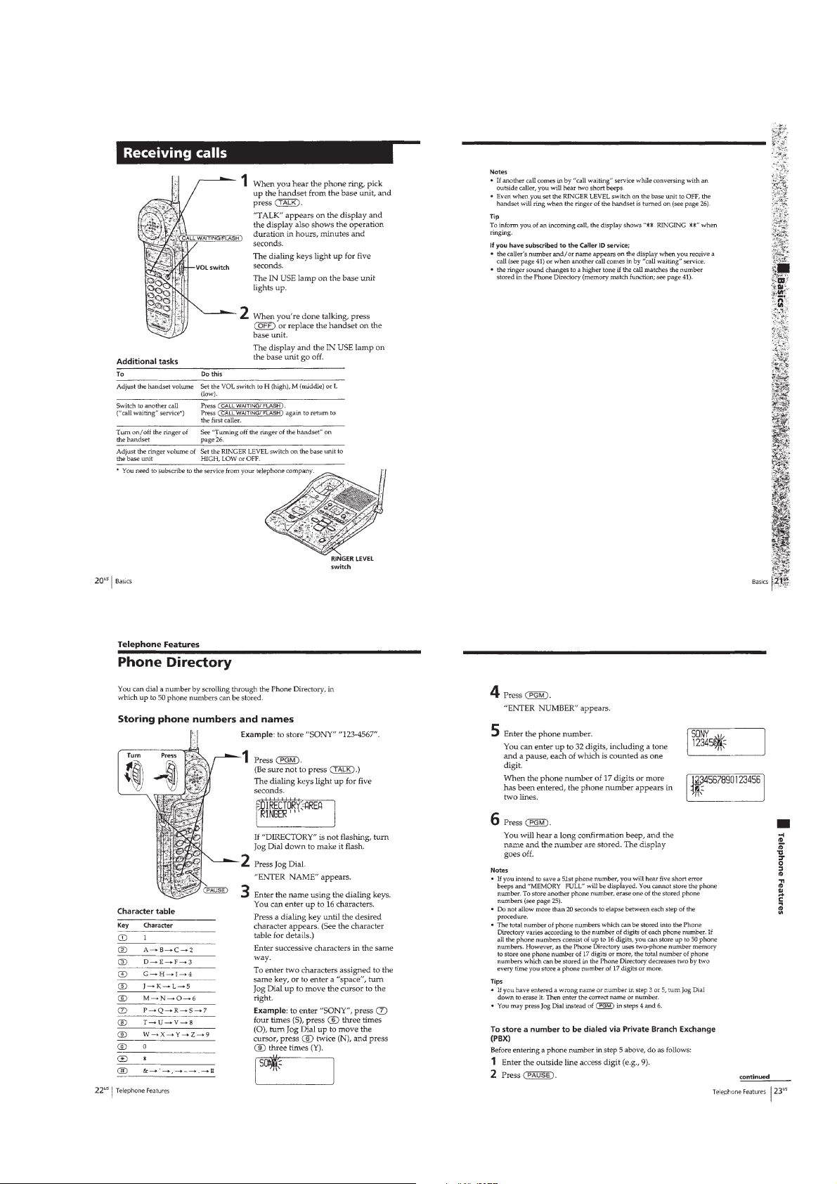
Phone Directory....................................................................... 7
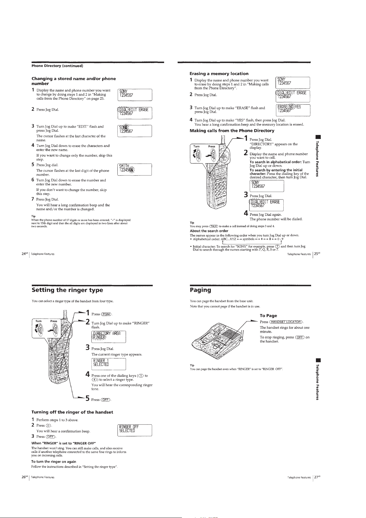
Setting the Ringer Type ........................................................... 8
Paging ......................................................................................8
Setting Up the Answering Machine......................................... 9
Playing Back Messages ......................................................... 10
Selecting the Announcement Only Mode.............................. 11
Screening Calls ...................................................................... 11
Recording a Memo Message ................................................. 11
Operating From an Outside Phone ........................................ 11
Understanding the Caller ID Service..................................... 12
Looking at the Caller ID List ................................................ 12
Using the Caller ID List ........................................................13
Using “Caller ID With Visual Call Waiting” Service............ 14
Mounting the Base Unit on a Wall ........................................ 14
– HAND MAIN BOARD (SIDE B) –
U1001
2. DISASSEMBLY
2-1. Case (Rear)........................................................................ 15
2-2. RF Unit (HS), Hand Main Board ...................................... 15
2-3. Base (Bottom) ................................................................... 16
2-4. Base Main Board............................................................... 16
2-5. RF Unit (BU) .................................................................... 17
2-6. Base Key Board ................................................................ 17
2-7. I-TAD Board ..................................................................... 18
3. ELECTRICAL ADJUSTMENTS
3-1. Handset.............................................................................. 19
3-2. Base Unit ........................................................................... 20
4. DIAGRAMS
4-1. Block Diagram –Base Unit Section– ................................21
4-2. Block Diagram –Handset Section– ................................... 23
4-3. Schematic Diagram –Base Main Section (1/2)– ............... 25
4-4. Schematic Diagram –Base Main Section (2/2)– ............... 27
4-5. Printed Wiring Board –Base Main Section– ..................... 29
4-6. Printed Wiring Board –I-TAD Section– ............................34
4-7. Schematic Diagram –I-TAD Section– .............................. 35
4-8. Printed Wiring Board –Base Key Section–....................... 37
4-9. Schematic Diagram –Base Key Section–.......................... 39
4-10. Printed Wiring Board –Hand Main Section– .................... 41
4-11. Schematic Diagram –Hand Main Section– ....................... 43
5. EXPLODED VIEWS
5-1. Handset Section................................................................. 47
5-2. Base Unit Section .............................................................. 48
6. ELECTRICAL PARTS LIST ........................................ 49
– 2 –
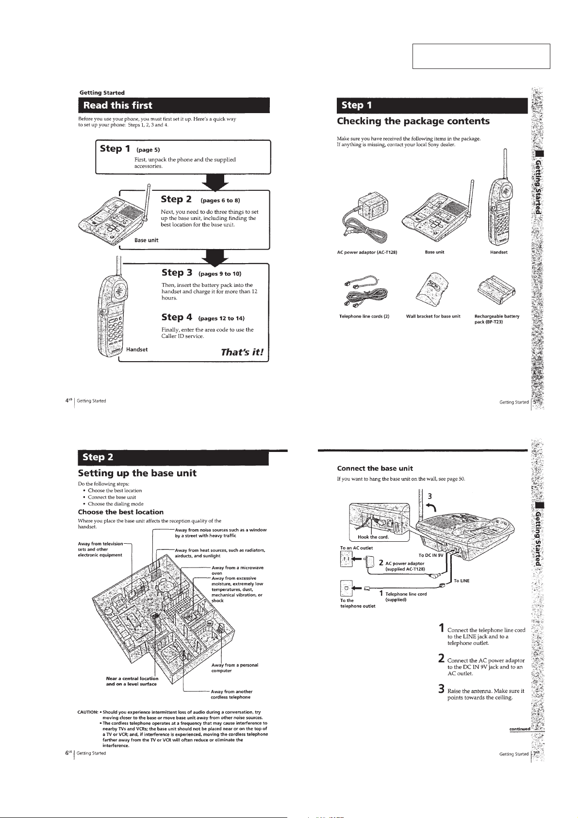
SECTION 1
GENERAL
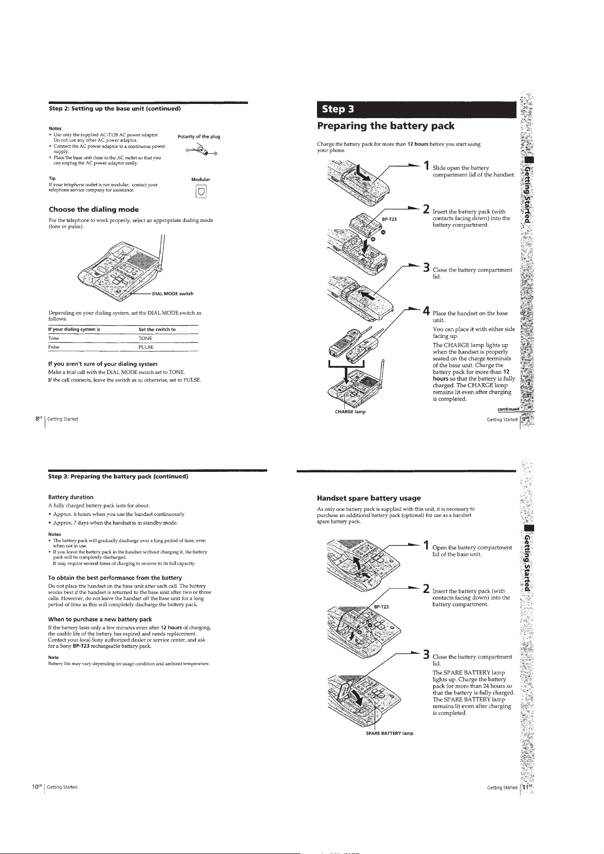
This section is extracted from
SPP-A974’s instruction manual.
– 3 –
– 4 –
– 5 –
– 6 –
– 7 –
– 8 –
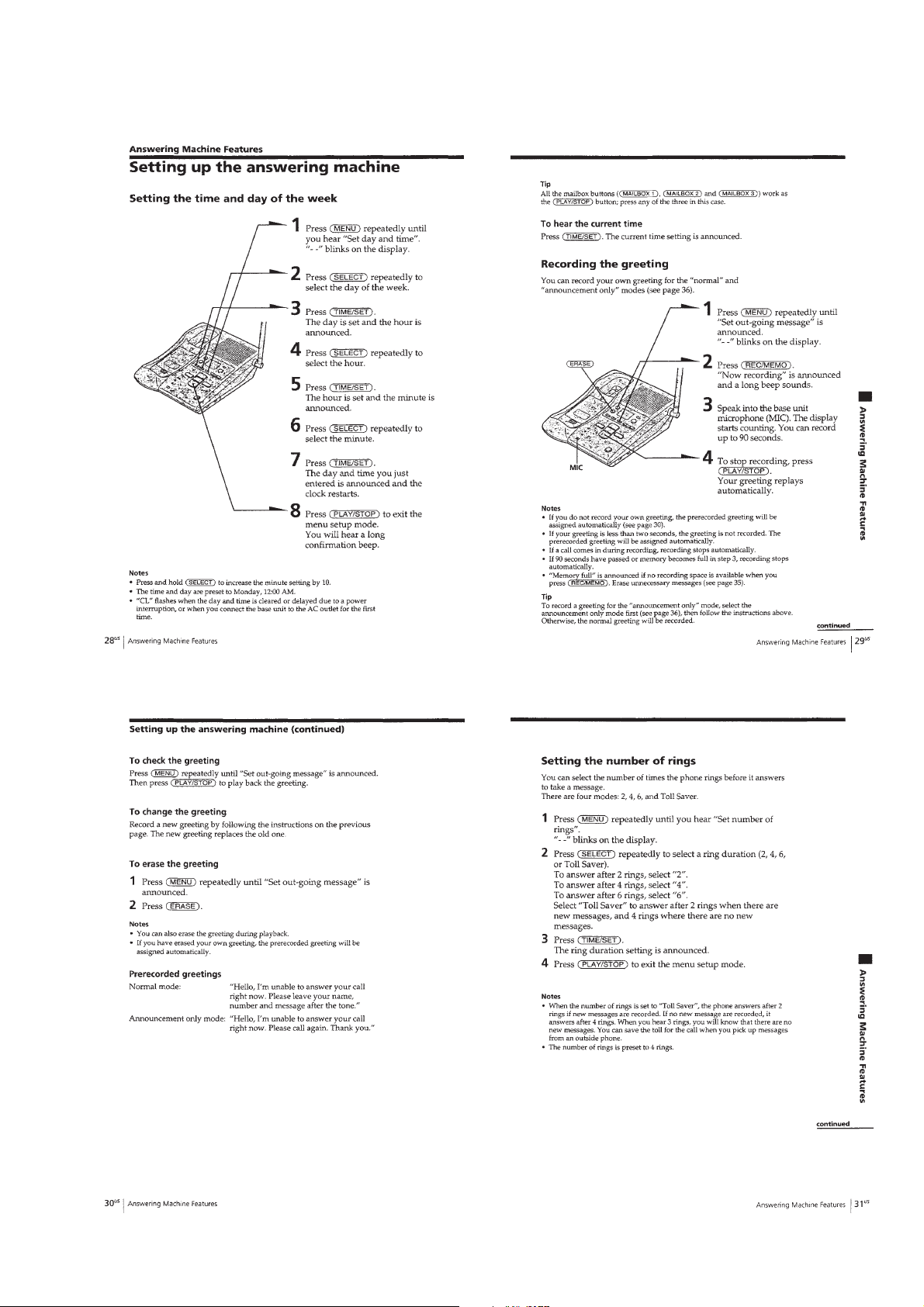
– 9 –
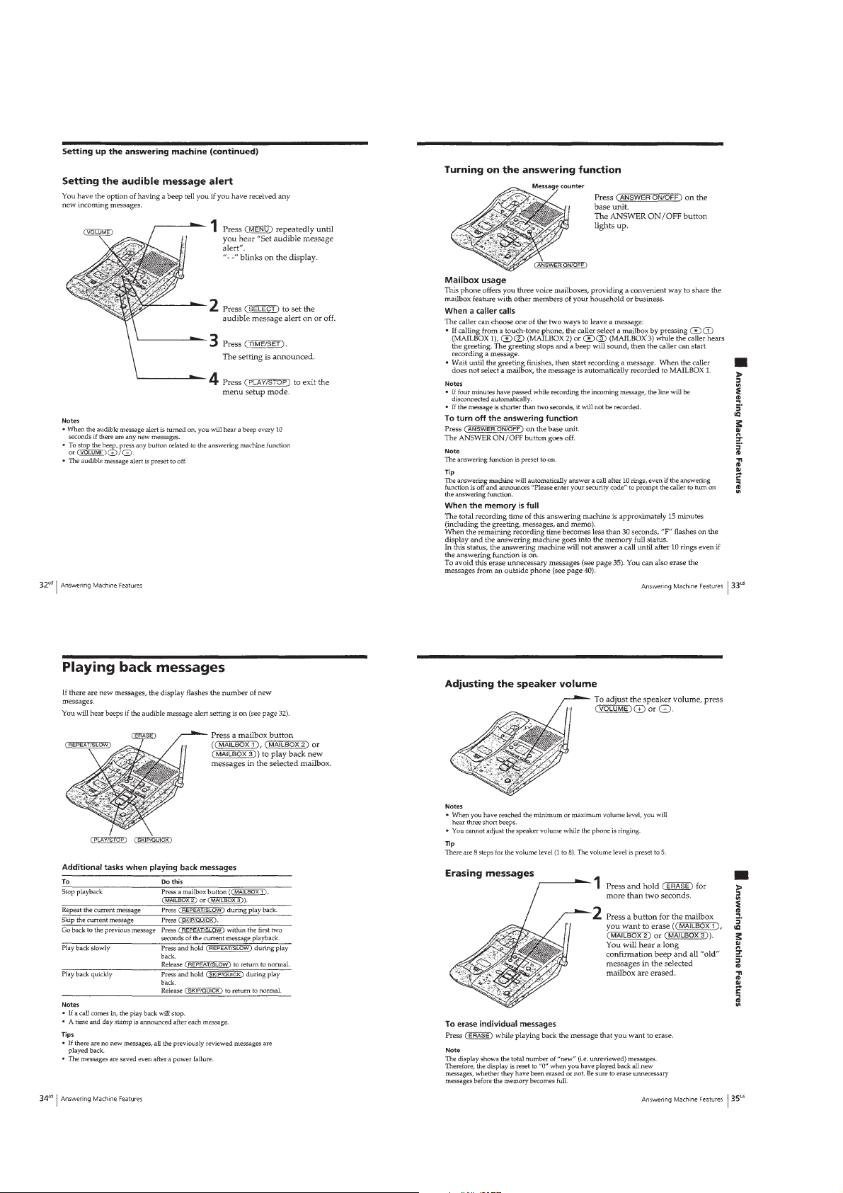
– 10 –
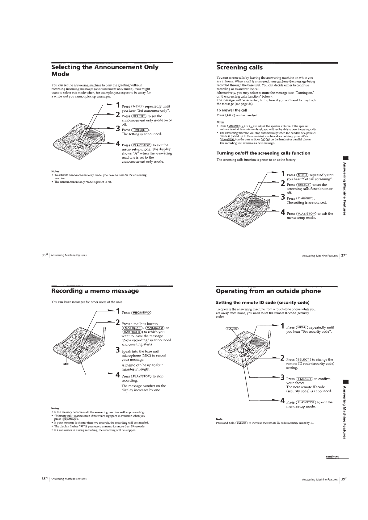
– 11 –
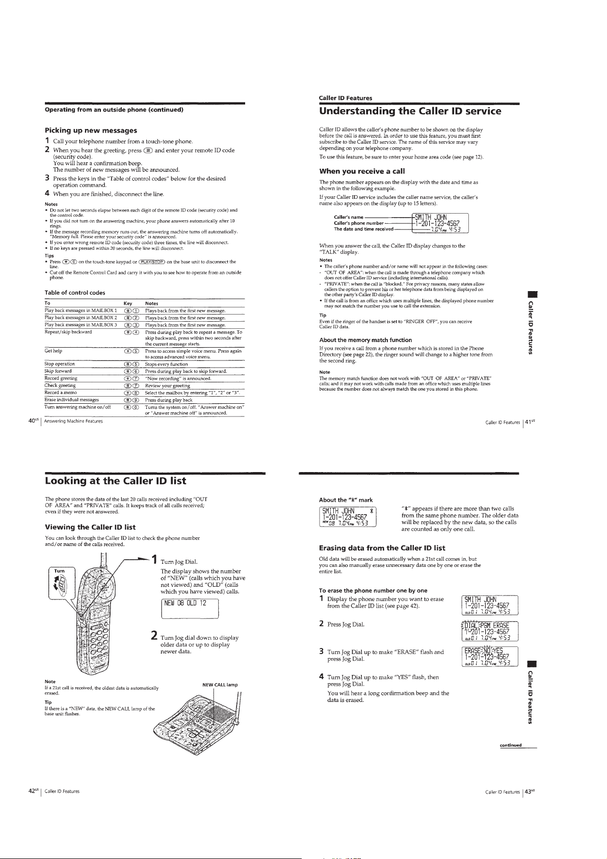
– 12 –
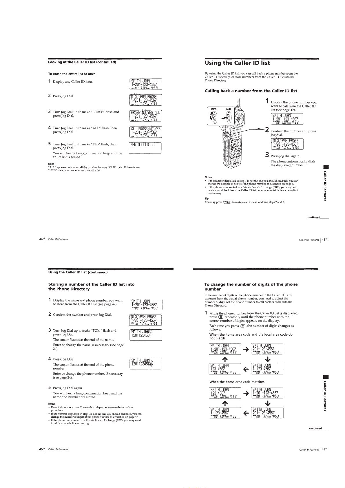
– 13 –
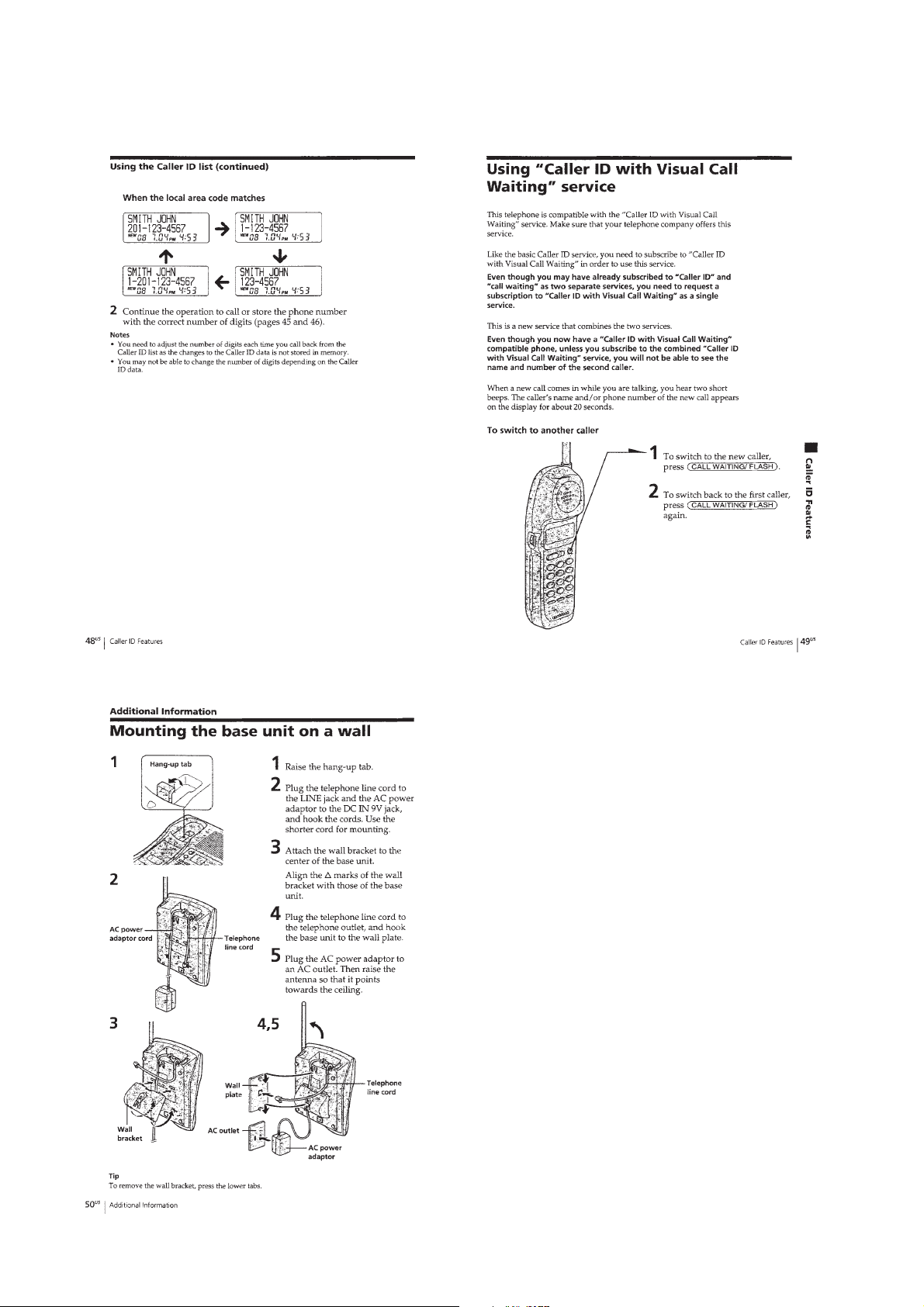
– 14 –
SECTION 2
DISASSEMBLY
• The equipment can be removed using the following procedure.
HANDSET CASE (REAR) RF UNIT (HS), HAND MAIN BOARD
BASE UNIT BASE (BOTTOM) BASE MAIN BOARD RF UNIT (BU) BASE KEY BOARD I-TAD BOARD
Note : Follow the disassembly procedure in the numerical order given.
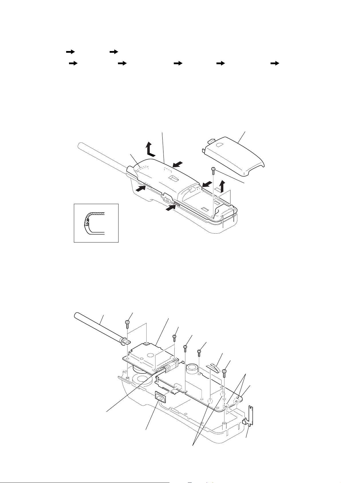
2-1. CASE (REAR)
battery case lid (HS)
2
claw
8
9
case (rear)
6
4
-
7
7
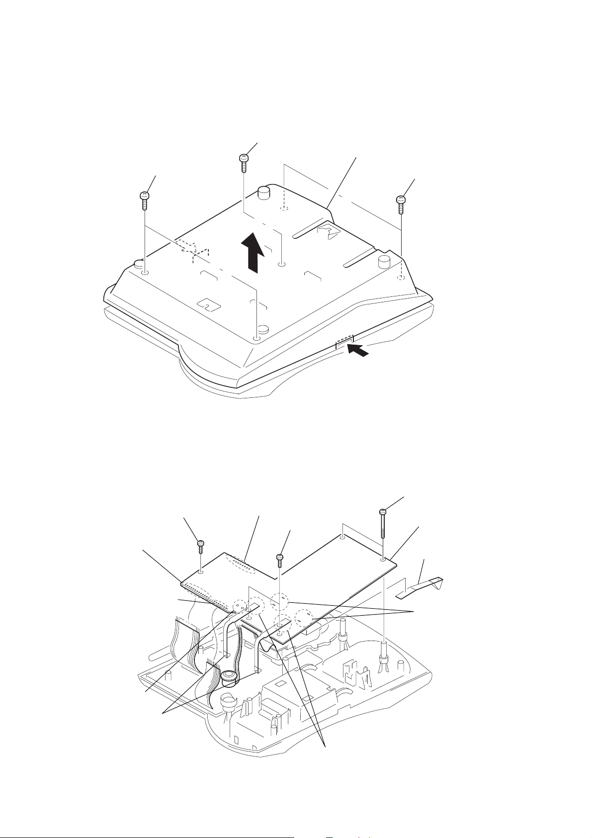
2-2. RF UNIT (HS), HAND MAIN BOARD
antenna
(ANT1001)
1
BTP 3x12
5
8
RF unit (HS)
2
B 2x8
4
4
B 2x6
5
B 2x6
battery terminals
1
3
BTP 3x12
3
BTP 3x12
7
Removal the solders.
6
VOL knob (HS)
– 15 –
0
Removal the solders.
9
Removal the solders.
qa
HAND MAIN board
charge terminals
2-3. BASE (BOTTOM)
3
BTP 3x12
5
2
BTP 3x12
6
base (bottom)
4
1
BTP 3x12
2-4. BASE MAIN BOARD
5
Removal the solders.
6
Removal the solders.
7
Removal the
solders.
charge springs
3
BTP 3x12
4
Removal the solders.
2
BTP 3x12
1
screws (3x30)
0
BASE MAIN board
battery terminal (BU)
8
Removal the solders.
– 16 –
9
Removal the solders.
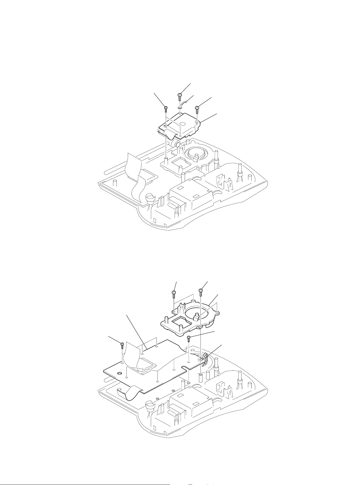
2-5. RF UNIT (BU)
3
B 2x8
1
BTP 3x12
lug
2
BTP 3x12
4
RF unit (BU)
2-6. BASE KEY BOARD
5
B 2x6
7
BASE KEY board
2
BTP 3x12
1
BTP 3x12
3
4
speaker holder
B 2x6
6
Removal the solders.
– 17 –
 Loading...