

SONY SPP-A973, SPP-974 Service Manual
SPP-A973/A974
SERVICE MANUAL
Ver 1.0 1999. 11
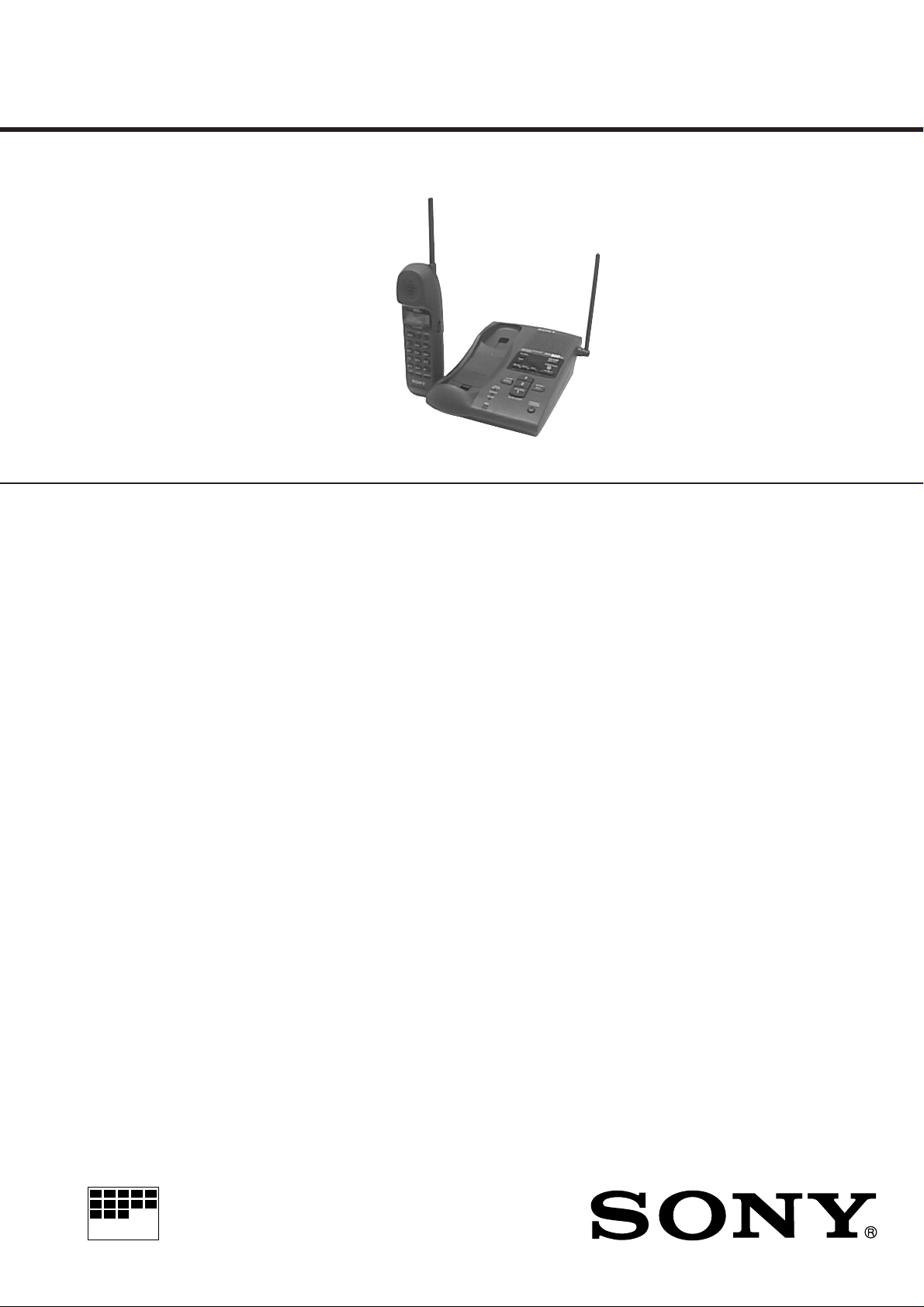
Photo: SPP-A973
SPECIFICATIONS
General
Frequency band (SPP-A973)
902 – 928 MHz
Frequency band (SPP-A974)
923.1 – 927.75 MHz
Base unit : 18 µW
Handset : 73 µW
Operating channel
30 channels
Dial signal
Tone, 10 PPS (pulse) selectable
Supplied accessories
AC power adaptor AC-T128 (1)
Telephone line cords (2)
Wall bracket for base phone (1)
Rechargeable battery pack BP-T23 (1)
Handset
Power source
Rechargeable battery pack BP-T23
Battery charging time
Approx. 12 hours
Battery life
Standby: Approx. 7 days
Talk : Approx. 6 hours
Dimensions
Approx. 58 × 177 × 46 mm (w/h/d),
antenna excluded
(approx. 2 3/8 × 7 × 1 13/16 inches)
Antenna: Approx. 72 mm
(approx. 2 7/8 inches)
Mass
Approx. 270 g
(approx. 9.5 oz), battery included
US Model
SPP-A973
Canadian Model
SPP-A974
Base unit
Power source
DC 9 V from AC power adaptor
AC-T128
Battery charging time
Approx. 24 hours
Dimensions
Approx. 160 × 63 × 225 mm (w/h/d),
antenna excluded
(approx. 6 3/8 × 2 1/2 × 8 7/8 inches)
Antenna: Approx. 120 mm
(approx. 4 3/4 inches)
Mass
Approx. 585 g
(approx. 1 lb 5 oz), wall bracket excluded
Answering machine
Maximum recording time
About 15 minutes, using incorporated IC
Greeting message
Up to 90 seconds per each
Incoming and Memo message
Up to 4 minutes per message
Design and specifications are subject to
change without notice.
Notes on Chip Component Replacement
• Never reuse a disconnected chip component.
• Notice that the minus side of a tantalum capacitor may be dam-
aged by heat.
MICROFILM
CORDLESS TELEPHONE
– 1 –
SPP-A973/A974
THIS NOTE IS COMMON FOR PRINTED WIRING
BOARDS AND SCHEMATIC DIAGRAMS.
(In addition to this, the necessary note is
printed in each block.)
For schematic diagrams
• All capacitors are in µF unless otherwise noted. pF: µµF
50 WV or less are not indicated except for electrolytics
and tantalums.
• All resistors are in Ω and 1/
specified.
• C : panel designation.
• U : B+ Line.
• Power voltage is dc 9 V and fed with regulated dc power
supply from external power voltage jack. (BASE PHONE)
• Power voltage is dc 12 V and fed with regulated dc power
supply from J1008 with 100 Ω in series. (BASE PHONE)
• Power voltage is dc 3 V and fed with regulated dc power
supply from battery terminal. (HANDSET)
• Voltage is dc with respect to ground under no-signal
condition.
• Voltages are taken with a VOM (Input impedance 10 MΩ).
Voltage variations may be noted due to normal production tolerances.
• Signal path.
N : TX (To Tel Line)
O : RX (From Tel Line)
P : bell
4
W or less unless otherwise
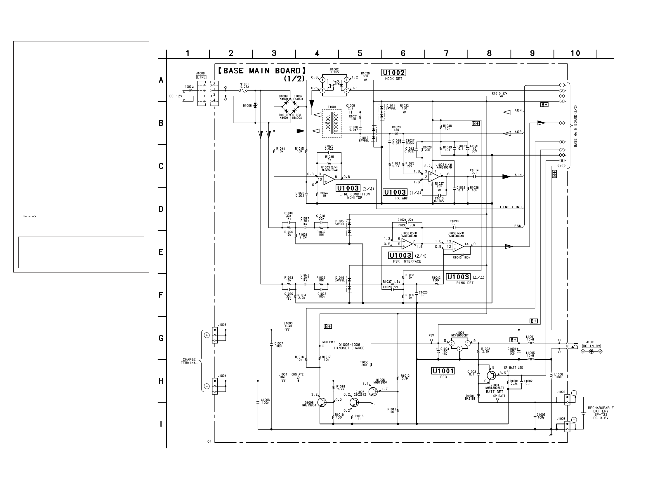
4-3. SCHEMATIC DIAGRAM — BASE MAIN SECTION (1/2) —
(Page 27)
For printed wiring boards
• X : parts extracted from the component side.
• : Carbon pattern.
z
•
• b : Pattern from the side which enables seeing.
Caution:
Pattern face side: Parts on the pattern face side seen from the
(Side B) pattern face are indicated.
Parts face side: Parts on the parts face side seen from the
(Side A) parts face are indicated.
: Through hole.
(The other layer’s patterns are not indicated.)
– 25 – – 26 –
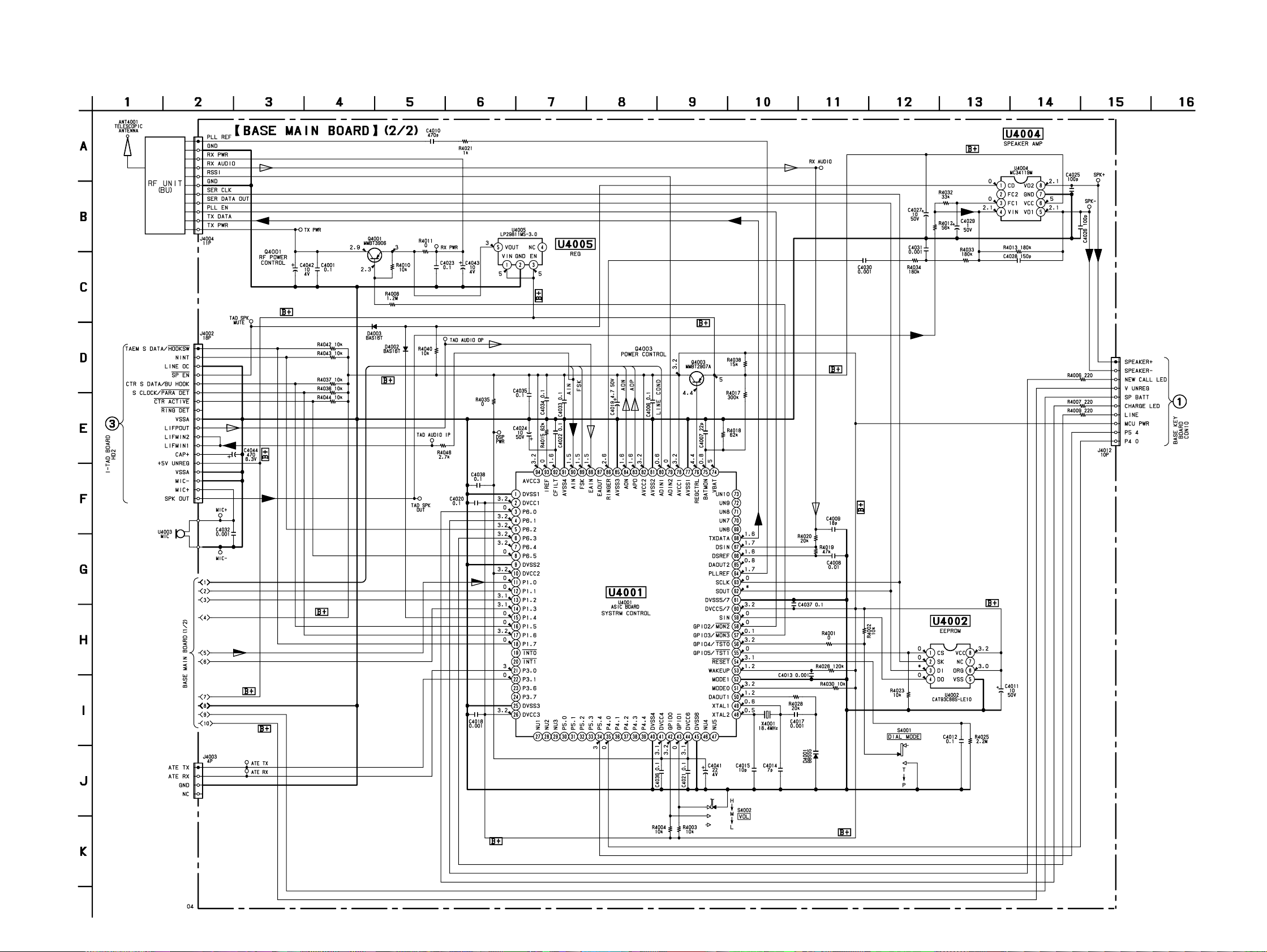
4-4. SCHEMATIC DIAGRAM — BASE MAIN SECTION (2/2) — • Refer to page 45 for IC Block Diagrams.
SPP-A973/A974
(Page 35)
(Page 40)
(Page 26)
– 27 – – 28 –
 Loading...