

Page 1
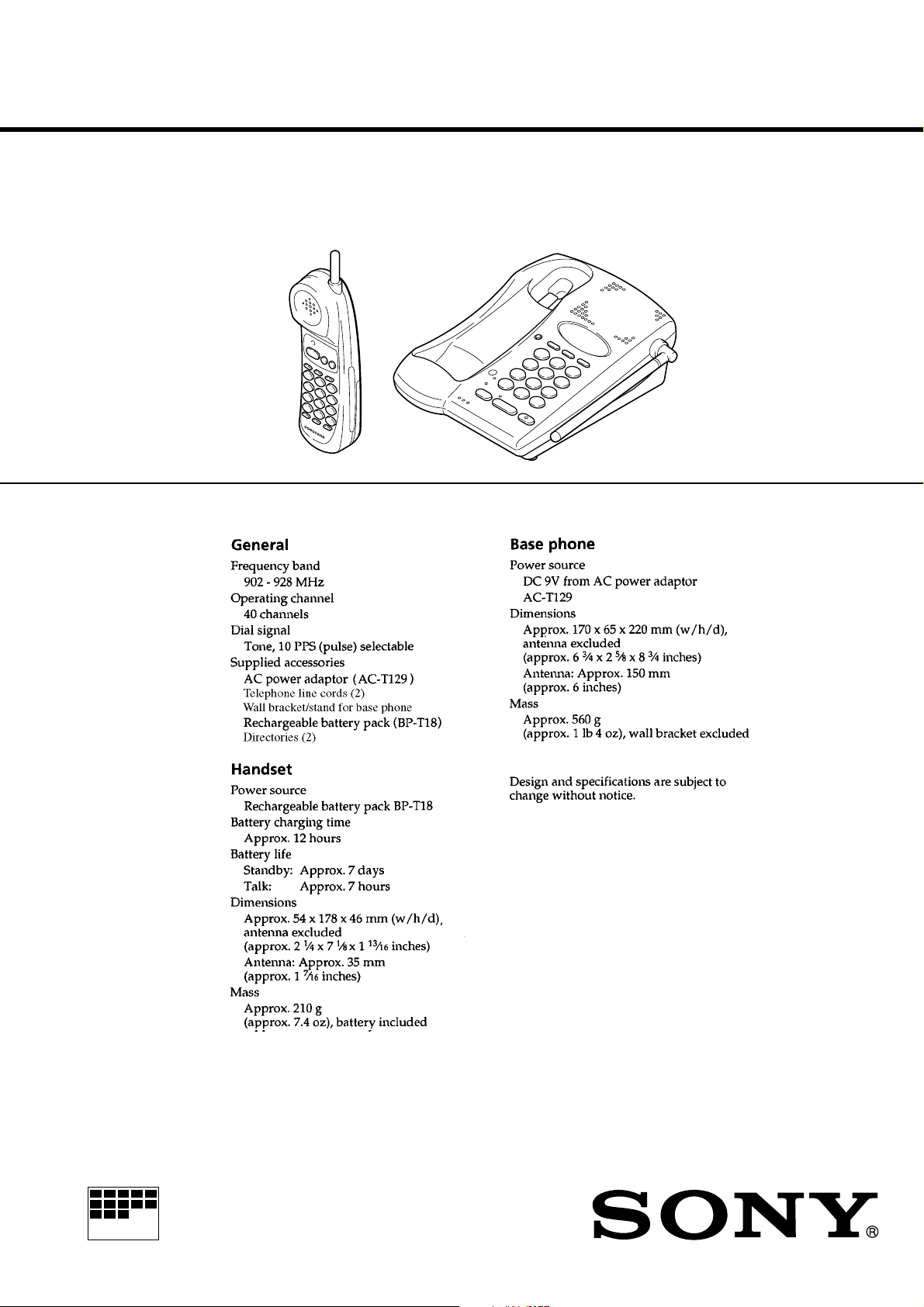
SPP-933/934
SERVICE MANUAL
Ver 1.0 2000. 01
SPECIFICATIONS
US Model
SPP-933
Canadian Model
Mexican Model
SPP-934
MICROFILM
CORDLESS TELEPHONE
Page 2

TABLE OF CONTENTS
1. GENERAL
Identifying the Parts ........................................................ 3
Setting Up the Base Phone ............................................. 3
Preparing the Battery Pack ............................................. 4
Making Calls ................................................................... 5
Receiving Calls ............................................................... 5
Telephone Features ......................................................... 6
2. DISASSEMBLY ......................................................... 9
3. TEST MODE
Base Unit ......................................................................... 12
Handset ............................................................................ 14
4. ELECTRICAL ADJUSTMENTS
Base Unit ......................................................................... 15
Handset ............................................................................ 17
5. DIAGRAMS
5-1. Block Diagram – BASE UNIT Section (1/2) –............. 19
5-2. Block Diagram – BASE UNIT Section (2/2) –............. 21
5-3. Block Diagram – HANDSET Section – ........................ 23
5-4. Note for Printed Wiring Boards and
Schematic Diagrams ....................................................... 25
5-5. Printed Wiring Board – BASE RF Section – ................ 26
5-6. Schematic Diagram – BASE RF Section – ................... 27
5-7. Printed Wiring Boards – BASE MAIN Section – ......... 29
5-8. Schematic Diagram – BASE MAIN Section – ............. 31
5-9. Printed Wiring Board – BASE KEY Section – ............. 34
5-10. Schematic Diagram – BASE KEY Section – ................ 35
5-11. Printed Wiring Board – HAND RF Section –............... 36
5-12. Schematic Diagram – HAND RF Section – .................. 37
5-13. Printed Wiring Board – HAND MAIN Section – ........ 39
5-14. Schematic Diagram – HAND MAIN Section – ............ 41
5-15. IC Pin Function Description ........................................... 45
Notes on chip component replacement
• Never reuse a disconnected chip component.
• Notice that the minus side of a tantalum capacitor may be damaged by heat.
6. EXPLODED VIEWS ................................................ 47
7. ELECTRICAL PARTS LIST ............................... 49
SAFETY-RELATED COMPONENT WARNING!!
COMPONENTS IDENTIFIED BY MARK 0 OR DOTTED
LINE WITH MARK 0 ON THE SCHEMATIC DIA GRAMS
AND IN THE PARTS LIST ARE CRITICAL TO SAFE
OPERATION. REPLACE THESE COMPONENTS WITH
SONY PARTS WHOSE PART NUMBERS APPEAR AS
SHOWN IN THIS MANU AL OR IN SUPPLEMENTS PUBLISHED BY SONY.
ATTENTION AU COMPOSANT AYANT RAPPORT
À LA SÉCURITÉ!
LES COMPOSANTS IDENTIFIÉS P AR UNE MARQUE 0
SUR LES DIAGRAMMES SCHÉMATIQUES ET LA LISTE
DES PIÈCES SONT CRITIQUES POUR LA SÉCURITÉ
DE FONCTIONNEMENT. NE REMPLACER CES COMPOSANTS QUE PAR DES PIÈCES SONY DONT LES
NUMÉROS SONT DONNÉS DANS CE MANUEL OU
DANS LES SUPPLÉMENTS PUBLIÉS PAR SONY.
– 2 –
Page 3

SECTION 1
GENERAL
This section is extracted from
instruction manual.
– 3 –
Page 4

– 4 –
Page 5

– 5 –
Page 6

– 6 –
Page 7

– 7 –
Page 8

– 8 –
Page 9
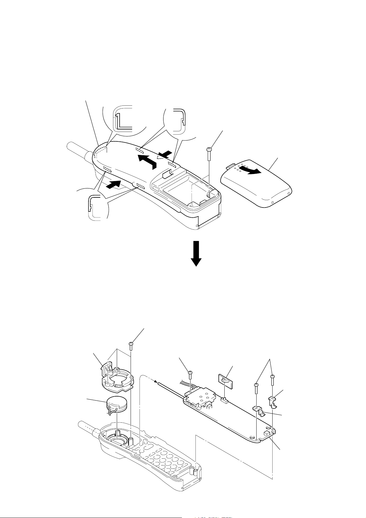
SECTION 2
d
)
DISASSEMBLY
Note: Follow the disassembly procedure in the numerical order given.
HAND CABINET (REAR)
5 Remove the hand cabinet (rear)
in the direction of arrow B.
4 claw
B
3 two claws
HAND MAIN BOARD, SPEAKER (SP801)
3 two claws
2 two screws
(BTP3 × 12)
1 Remove the battery case li
in the direction of arrow A.
A
7 holder (SP)
8 speaker
(SP801)
6 three screws
(BTP2.6 × 8)
3 screw
(BTP2.6 × 8)
1 knob
2 two screws
(BTP2.6 × 12)
4 charge terminal (L
4 charge terminal (R)
5 HAND MAIN board
– 9 –
Page 10

CABINET (LOWER) ASSY
y
2 three claws
1 four screws
(BTP2.6 × 12)
3 cabinet (lower) ass
BASE KEY BOARD
3 two screws
(BTP2.6 × 8)
5 speaker
(SP701)
4 holder (SP)
1 eight screws
(BTP2.6 × 8)
2 BASE KEY board
– 10 –
Page 11

BASE MAIN BOARD
6 two screws
(BTP2.6 × 8)
7 BASE MIC board
3 seven screws
(BTP2.6 × 8)
2 flat cable
1 knob (VR)
3 four screws
(BTP2.6 × 8)
4 spring washer
5 BASE MAIN board
– 11 –
Page 12
SECTION 3
TEST MODE
BASE UNIT
[Setting the Test Mode]
1. Power on with pressing the [*] and [#] keys for a second.
2. When the test mode is set, it beeps confirm tone and SPEAKERPHONE LED turns on for 50 msec.
Note: If setting the test mode with the status that [TONE] position is selected at [DIAL MODE] switch, the unit cold stars next time when the power is
turned on.
[Releasing the Test Mode]
To release the test mode, perform as follows:
• Turn the power off (disconnect the AC adapter plug).
• Set the handset to charge on the base unit.
• Bell in.
• Press the [SPEAKERPHONE] key.
• Press the [INTERCOM] key.
[Changing the Test Mode No.]
Press each key of the test mode No.
[Changing the Channel]
Press the [REDIAL/PAUSE] key.
Note: Channel will be back to initial channel (19CH), when the test mode step is changed.
• Channel Rotation
21CH 40CH 1CH 2CH 3CH 39CH 40CH20CH19CH
. . .
– 12 –
Page 13
[Test Mode Execution]
Press each key for the desired test mode No. to execute any of the following tests:
No.
1 VCO/TX FREQ. ADJ 1 L L H H L H
2 TX MOD CHECK 2 H L H H L L
3 TX DATA 3 L L H H L H *1
4 RX SENS 4 L H H H L L
5 SQ SENS 5 L H/L H H L/H L *2
6 BELL CHECK 6 L L H H L/H H *3
7 DTMF DUAL TONE 7 L L H H L L *4
8 DATA IN CHECK 8 L L H H L L *5
9 CHANNEL DATA 9 L L H H L H *6
10 DUPLEX 0 H H H H L L
11 INTERCOM PGM H H L L H H
Test Mode
Name
KEY
TX MUTE (IC8 pin qj)
SP MUTE1 (IC8 pin ef)
SP MUTE2 (IC8 pin rh)
LINE MUTE (IC8 pin rg)
MIC MUTE (IC8 pin qg)
RX MUTE (IC8 pin eh)
*Initial Channel of each test mode No.: 19CH
*1. Test Mode 3: Continue output TX data as “ 0000……”.
*2. Test Mode 5: When signal is detected, it rings bell tone.
*3. Test Mode 6: Output level of the bell can be changed by the [RINGER] switch (S2).
*4. Test Mode 7: Press the [FLASH] key.
DTMF will be changed.
1 → 2 → 3 → 4 → 5 → 6 → 7 → 8 → 9 → 0 → → # → 1 → …… .
*
*5. Test Mode 8: When locked receiving data is “ 0000……”, it rings bell tone.
*6. Test Mode 9: Continue output data as “ 1111……” from CHG CONT(IC8 pin qh).
Remarks
– 13 –
Page 14
HANDSET
[Setting the Test Mode]
1. Power on with press the [*] key and the [#] key simultaneously for one second.
2. It beeps confirm tone, and the test mode is set.
Note: If the [PGM] key is pressed, the unit cold starts next time when the power is turned on.
[Releasing the Test Mode]
To release the test mode, perform as follows:
• Press the [TALK] key.
• Turn the power off (remove the battery pack).
• Set the handset to charge on the base unit (except Test Mode 9).
[Changing the Test Mode No.]
Press the each key of the test mode No.
[Changing the Channel]
Press the [CHANNEL] key.
Note: The channel is back to initial channel (21CH), when test mode No. is changed.
• Channel Rotation
19CH 40CH 1CH 2CH 3CH 39CH 40CH20CH21CH
[Test Mode Execution]
Press the each key for the desired test mode No. to execute any of the following tests:
No.
1 VCO/TX FREQ. ADJ 1 L H L L H
2 TX MOD CHECK 2 L H H L L
3 TX DATA 3 L H L L L *1
4 RX SENS 4 H H L H L
5 SQ SENS 5 L H L *A L
6 RECEIVE DATA CHECK 6 L H L L H *2
7 BELL CHECK 7 L L L L H *3
8 BAT. LOW CHECK 8 L L L L H *4
9 CHARGE CHECK 9 L L L L H *5
10 DUPLEX 0 L H H H L
Test Mode
Name
KEY
SC (IC603 pin qd)
TX B (IC603 pin rs)
RX MUTE (IC603 pin qs)
TX MUTE (IC603 pin qa)
CONV (IC603 pin ej)
*Initial Channel of each test mode No.: 21CH
. . .
Remarks
*A. SQ on: H
SQ off: L
*1. Test Mode 3: Continue output TX data as “ 0000……”.
*2. Test Mode 6: When locked receiving data is “ 0000……”, it beeps confirm tone. (1 kHz)
*3. Test Mode 7: It rings with “ H” level.
*4. Test Mode 8: When BATT LOW (IC603 pin eg) is “ L” (battery low), it beeps confirm tone.
*5. Test Mode 9: When CHG IN (IC603 pin eh) is “ L” (charge on), it beeps confirm tone.
– 14 –
Page 15

SECTION 4
ELECTRICAL ADJUSTMENTS
0 dBm = 0.775 V, 0 dBV = 1 V
BASE UNIT
• Make the set in test mode. (See page 12)
• Remove the solder of the BP (ANT) on the BASE MAIN board
when performing adjustments. After completing the adjustments,
short the BP (ANT) by solder.
– TX Adjustments –
1. TX Power Adjustment
Setting:
power meter
+
–
Procedure:
1. Connect a power meter to TP (ANT) and TP (GND) on the
BASE MAIN board.
2. Adjust RT301 on the B ASE RF board (the BASE RF board is
mounted on the BASE MAIN board) so that the value of po wer
meter becomes –6.5 dBm.
2. TX Frequency Adjustment
Setting:
frequency counter
TP (ANT)
TP (GND)
– RX Adjustments –
1. DISCRI V oltage Adjustment
Setting:
SSG
TP (ANT)
Carrier frequency: 902.902467 MHz
Modulation: no modulation
Output level: – 47 dBm
digital voltmeter
+
–
TP (DISCRI)
TP (GND)
TP (GND)
Procedure:
1. Connect a SSG to TP (ANT) and TP (GND) on the BASE
MAIN board.
2. Connect a digital voltmeter to TP (DISCRI) and TP (GND) on
the BASE MAIN board.
3. Press the [4] key to change the test mode step to RX SENS.
4. Adjust L3 on the BASE MAIN board so that the value of digital voltmeter becomes 1 V.
2. TEL Out Level Adjustment
Setting:
+
–
TP (ANT)
TP (GND)
Procedure:
1. Connect a frequency counter to TP (ANT) and TP (GND) on
the BASE MAIN board.
2. Adjust CT1 on the BASE MAIN board so that the value of
frequency counter becomes 926.897468 MHz.
3. Modulation Sensitivity Adjustment
Setting:
AF OSC
600 Ω
+
–
1 kHz, –20 dBm
deviation meter
+
–
LINE jack (J1)
TP (ANT)
TP (GND)
Procedure:
1. Connect an AF OSC to the LINE jack (J1) on the BASE MAIN
board.
2. Connect a deviation meter to TP (ANT) and TP (GND) on the
BASE MAIN board.
3. Press the
[2] key to change the test mode step to TX MOD
CHECK.
4. Adjust RT3 on the BASE MAIN board so that the value of
deviation meter becomes ±8 kHz deviation.
SSG
TP (ANT)
Carrier frequency: 902.902467 MHz
Modulation: 1 kHz, ±8 kHz deviation
Output level: – 47 dBm
noise meter
600 Ω
+
–
TP (GND)
LINE jack (J1)
Procedure:
1. Change the modulation of SSG to 1 kHz, ±8 kHz deviation.
2. Connect a noise meter to the LINE jack (J1) on the BASE
MAIN board.
3. Adjust RT2 on the BASE MAIN board so that the value of
noise meter becomes –11.5 dBm.
– 15 –
Page 16

3. SQ Sensitivity Adjustment
Setting:
SSG
TP (ANT)
Carrier frequency: 902.902467 MHz
Modulation: no modulation
Output level: –114 dBm
TP (GND)
Procedure:
1. Change the modulation to no modulation and change the output level of SSG to –114 dBm.
2. Press the [5] key to change the test mode step to SQ SENS.
3. Adjust RT1 on the BASE MAIN board so that the speakerphone (SP701) rings bell tone continuously.
Adjustment Location:
– BASE MAIN BOARD (Component Side) –
– BASE MAIN BOARD (Conductor Side) –
J1
TX Frequency Adjustment
RT3
Modulation Sensitivity Adjustment
RT1
SQ Sensitivity Adjustment
RT2
TEL Out Level Adjustment
RT301
TX Power Adjustment
CT1
L3
DISCRI Voltage Adjustment
BP (ANT)
TP (ANT)
TP (GND)
TP (DISCRI)
– 16 –
Page 17

HANDSET
– RX Adjustments –
• Make the set in test mode. (See page 14)
• Remove the solder of the BP (ANT) on the HAND MAIN board
when performing adjustments. After completing the adjustments,
short the BP (ANT) by solder.
– TX Adjustments –
1. TX Power Adjustment
Setting:
power meter
+
–
TP (ANT)
TP (GND)
Procedure:
1. Connect a power meter to TP (ANT) and TP (GND) on the
HAND MAIN board.
2. Adjust RT501 on the HAND RF board so that the value of
power meter becomes –6.5 dBm.
2. TX Frequency Adjustment
Setting:
frequency counter
+
–
TP (ANT)
TP (GND)
1. DISCRI V oltage Adjustment
Setting:
SSG
TP (ANT)
Carrier frequency: 926.997467 MHz
Modulation: no modulation
Output level: – 47 dBm
digital voltmeter
+
–
TP (DISCRI)
TP (GND)
TP (GND)
Procedure:
1. Connect a SSG to TP (ANT) and TP (GND) on the HAND
MAIN board.
2. Connect a digital voltmeter to TP (DISCRI) and TP (GND) on
the HAND MAIN board.
3. Press the [4] key to change the test mode step to RX SENS.
4. Adjust L602 on the HAND MAIN board so that the value of
digital voltmeter becomes 0.95 V.
2. Speaker Out Level Adjustment
Setting:
SSG
Procedure:
1. Connect a frequency counter to TP (ANT) and TP (GND) on
the HAND MAIN board.
2. Restart the test mode to change the channel to 21CH.
3. Adjust CT601 on the HAND MAIN board so that the value of
frequency counter becomes 926.997467 MHz.
3. Modulation Sensitivity Adjustment
Setting:
AF OSC
600 Ω
+
–
1 kHz, 9 mV
deviation meter
+
–
TP (MIC+)
TP (MIC–)
TP (ANT)
TP (GND)
Procedure:
1. Disconnect the microphone (MC601) on the HAND MAIN
board.
2. Connect an AF OSC to TP (MIC+) and TP (MIC–) on the
HAND MAIN board.
3. Connect a deviation meter to TP (ANT) and TP (GND) on the
HAND MAIN board.
4. Press the [2] key to change the test mode step to TX MOD
CHECK.
5. Adjust RT603 on the HAND MAIN board so that the value of
deviation meter becomes ±8 kHz modulation.
TP (ANT)
Carrier frequency: 926.997467 MHz
Modulation: 1 kHz, ±8 kHz deviation
Output level: – 47 dBm
noise meter
150 Ω
+
–
TP (GND)
TP (SP1)
TP (SP2)
Procedure:
1. Change the modulation of SSG to 1 kHz, ±8 kHz deviation.
2. Disconnect the speaker (SP801).
3. Connect a noise meter to TP (SP1) and TP (SP2) on the HAND
MAIN board.
4. Set the
[VOL] switch (S601) to [M] position.
5. Adjust RT602 on the HAND MAIN board so that the value of
noise meter becomes –18.5 dBV.
– 17 –
Page 18

3. SQ Sensitivity Adjustment
Setting:
SSG
TP (ANT)
Carrier frequency: 926.997467 MHz
Modulation: 1 kHz, ±8 kHz deviation
Output level: –113 dBm
TP (GND)
Procedure:
1. Change the output level of SSG to –113 dBm.
2. Press the [5] key to change the test mode step to SQ SENS.
3. Adjust RT601 so that the TALK/BATT LOW LED (D607)
becomes blinking.
Adjustment Location:
– HAND MAIN BOARD –
(Component Side)
HAND RF Board
RT501
TX Power Adjustment
TX Frequency Adjustment
CT601
– HAND MAIN BOARD –
(Conductor Side)
TP (SP1)
TP (SP2)
BP (ANT)
TP (MIC+)
TP (MIC–)
TP (ANT)
TP (GND)
DISCRI Voltage Adjustment
L602
RT602
Speaker Out Level Adjustment
RT603
Modulation Sensitivity Adjustment
RT601
SQ Sensitivity Adjustment
TP (DISCRI)
– 18 –
Page 19

SECTION 5
DIAGRAMS
5-1. BLOCK DIAGRAM – BASE UNIT Section (1/2) –
SPP-933/934
ANT701
(ANTENNA)
B.P.F.
FT301
TX AMP
Q306, 307
RF AMP
RT301
TX
POWER
Q301
TX B+
SWITCH
Q302
1st MIXER, VCO, PLL SYNTHESIZER
24
TX B+
(3V)
14
MIX
IN
MIXER
LOCAL OSC
BUFFER
(RX SYSTEM)
LOCK
IC302
1st
VCO
MIX
OUT
RXE
RXB
13
10.555MHz
20
21
FT1
RX VCO
Q312
IF AMP
Q1
X1
10.1MHz
CT1
TX
FREQUENCY
L.P.F.
D303
LOCK
DETECTOR
2nd MIXER, LIMITER AMP, DET,
AF AMP, SQUELCH CONTROL
16
MIX
IN
18
2nd
MIXER
LOCAL
OSC
OSC
1 2
PD2
IC3
OSC
MIX
OUT
3
PHASE
DETECTOR
FT2
455kHz
LIM
IN
5
PROGRAM-
MABLE
DIVIDER
LATCH
DISCRI
VOLTAGE
LIMITER
AMP
SQUELCH
TRIGGER
WITH
HYSTERESIS
SCAN
CONTROL
13
L3
QUAD COIL
MODULATOR
12
LEVEL SHIFT
1/32, 1/33
PRESCALER
DE-
B+ (3V)
RT2
8
AF
OUT
AF
AMP
FIL
OUT
FILTER
AMP
Q8
9
FIL
INSQ IN
1011
RT3
MODULATION
SENSITIVITY
SENSITIVITY
TEL
OUT LEVEL
RT1
SQ
LEVEL SHIFT
47 48 20
18
SQ IN
DATA EN
DATA OUT
SYSTEM CONTROLLER
IC8 (1/2)
TX MUTE
RX MUTE
PREAMP
Q2
Q5, 6
DATA IN
EPI
5
PREANP
CO CPI
10
17
36
EXPANDER
CIRCUIT
MUTE
MUTE C
EXPANDER, COMPRESSOR
IC1
MUTE
COMPRESSOR
CIRCUIT
MUTE E
211
EO
3
PREAMPLIMITER
7
TX
RX
(Pege 21)
A
(Pege 21)
B
TX
OUT
2
• SIGNAL PATH
: RX
: TX
: BELL
05
2 DOUBLER
TX AMP
VCO
(TX SYSTEM)
TXE
TXB
PROGRAM-
5
4
TX
VCO
L.P.F.
D302
PD1
7
PHASE
DETECTOR
1/2
MABLE
DIVIDER
LATCH
PROGRAM-
MABLE
DIVIDER
LATCH
1/16, 1/17
PRESCALER
OSC &
1/2 DIVIDER
SHIFT
REGISTER &
LATCH
PULSE
COUNTER
XIN
XOUT
CPS
SI
RST
9
10
16
15
17
12
13
11
PLL DATA
PLL CLK
PLL EN
– 19 – – 20 –
Page 20

SPP-933/934
5-2. BLOCK DIAGRAM – BASE UNIT Section (2/2) –
(Pege 20)
(Pege 20)
A
B
BUFFER
IC6 (1/2)
BUFFER
IC6 (2/2)
+
+
+
AF AMP
IC4 (1/2)
RX LINE MUTE
Q7
VOICE SPEAKERPHONE
IC5
TX LINE MUTE
Q3
AF AMP
IC4 (2/2)
HIBRID AMP
Q4
T1
LINE
TRANSFORMER
RECT
D14, 15, 17, 18
PARA DETECT
IC9, Q20, 21
HOOK ON/OFF
RELAY DRIVE
Q18
RINGER DETECT
IC2
J1
LINE
• SIGNAL PATH
: RX
: TX
: BELL
1
DTMF
+
X0
X2
3.579545MHz
4
27
5
7
SYSTEM CONTROLLER
X1
TXO
RXI
ATT
CONTROL
TLI
TX DET
RLI
RX DET
IC8 (2/2)
ROW0 – ROW4
27 – 31
KEY MATRIX
S701-719
TRANSMIT
ATT
RECEIVER
ATT
COMPRESSOR
TX/RX DET
COMPRESSOR
COL0 – COL3
TX DET
23 – 26
TXI
3 10 9
VR1
VOLUME
RXO
XDI
VLC
26
13
24
BELL HI
H L OFF
SPEAKER MUTE
Q16
34
SP MUTE1
BELL LOW
S2
RINGER
AF AMP
Q12
TONE/PULSE
S1
DIAL MODE
PULSE TONE
MCO
SKI
SPEAKER
19 15
++
LIMITER
38
44
RING VOL
BELL OUT
PEAK
MIC
AMP
AMP
AGC
17
46
SP MUTE2
D752
INTERCOM
MCI
SKO
INT LED
SP701
(SPEAKER)
SP LED
D753
SPEAKERPHONE
35333240424165
D754
LINE
LINE LED
MIC MUTE
Q10
15
MIC MUTE
MC1
MIC
45
LINE MUTE
22
PARADET
10
RLCONT
PWR OFF
RESET
37
BELL IN
39
2
RESET SIGNAL
GENERATOR
Q15
SYSTEM CONTROLLER
B+ (5V)
B+ (5V)
VOLTAGE DETECT
IC7
D7
D10
S701 S702 S703
1 2 ABC 3 DEF
S706 S707 S708
4 GHI 5 JKL 6 MNO
S710 S711 S712
7 PQRS 8 TUV 9 WXYZ
S715 S716 S717
05
0 OPER # TONE
S704
SPEED DIAL SPEAKERPHONE
REDIAL/PAUSE
S713
PGM
S718
INTERCOM
S705
S709
S714
FLASH
S719
HOLD
CHG CONT
B+ (3V)
TX B+
(3V)
16
B+ SWITCH
(FOR TX SYSTEM)
Q9
+3V REGULATOR
Q14
B+ (8V)
+6V REGULATOR
+8V REGULATOR
CHARGE CONTROL
Q13
Q17
Q19
–
DC IN 9V
+
J2
+
CHARGE
TERMINAL
–
CHG DET
21
D751
CHARGE
CHARGE DETECT
Q11
– 21 – – 22 –
Page 21

SPP-933/934
5-3. BLOCK DIAGRAM – HANDSET Section –
W601
(ANTENNA)
TX AMP
Q506, 507
RT501
TX
POWER
RF AMP
Q501
B.P.F.
FT501
SWITCH
TX B+
Q502
1st MIXER, VCO, PLL SYNTHESIZER
24
TX B+
(3V)
14
MIX
IN
MIXER
LOCAL OSC
BUFFER
(RX SYSTEM)
LOCK
IC502
1st
VCO
MIX
OUT
RXE
RXB
13
10.555MHz
20
21
FT601
RX VCO
Q512
IF AMP
Q601
X601
10.1MHz
CT601
TX
FREQUENCY
L.P.F.
D503
LOCK
DETECTOR
2nd MIXER, LIMITER AMP, DET,
AF AMP, SQUELCH CONTROL
IC601
MIX
IN
16
18
2nd
MIXER
LOCAL
OSC
OSC
1 2
PD2
OSC
MIX
OUT
PHASE
DETECTOR
L602
DISCRI
VOLTAGE
FT602
455kHz
3
LIM
IN
5
PROGRAM-
MABLE
DIVIDER
LATCH
LIMITER
AMP
SQUELCH
TRIGGER
WITH
HYSTERESIS
SCAN
CONTROL
13
QUAD COIL
MODULATOR
12
1/32, 1/33
PRESCALER
DE-
B+ (3V)
RT602
8
AF
OUT
AF
9
FIL
INSQ IN
1011
RT603
MODULATION
SENSITIVITY
FIL
OUT
AMP
FILTER
AMP
SPEAKER
OUT LEVEL
RT601
SQ
SENSITIVITY
44 4541
SQ IN
DATA OUT
SYSTEM CONTROLLER
IC603
PREAMP
Q602
LEVEL SHIFT
Q603, 604
40
DATA E N
TX MUTE
RX MUTE
CONV
EPI
5
PREAMP
CO CPI
10
DATA I N
11
12
37
EXPANDER
CIRCUIT
MUTE
MUTE C
EXPANDER, COMPRESSOR
IC602
MUTE
COMPRESSOR
CIRCUIT
MUTE E
211
EXPANDER, COMPRESSOR
(IC602) B+
EO
3
L
PREAMPLIMITER
7
B+ SWITCH
Q611
AF AMP
Q607, 608
S601
VOL
MH
MIC AMP
Q404
SP801
(SPEAKER)
MC601
(MIC)
TX
OUT
2
2 DOUBLER
TX AMP
• SIGNAL PATH
: RX
: TX
: BELL
05
VCO
(TX SYSTEM)
TXE
TXB
D607
RINGER DRIVE
Q613
(KEY BACK LIGHT)
BATT B+
VDET1
1
VDET2
5
BATTERY
VOLTAGE DETECT
IC605
(SPP-934)
D609 – 612
B+ (3V)
TX B+ (3V)
COMPARATOR
COMPARATOR
PROGRAM-
PAUSE
MABLE
DIVIDER
LATCH
PROGRAM-
MABLE
DIVIDER
LATCH
5
4
TX
VCO
L.P.F.
D502
PD1
7
S601 S602 S603 S604 S605
HOLD INTERCOM CHANNEL TALK TONE
S606 S607 S608 S609 S610
1 2 ABC 3 DEF OFF 0 OPER
S611 S612 S613 S614 S615
4 GHI 5 JKL 6 MNO FLASH #
S616 S617 S618
7 PQRS 8 TUV 9 WXYZ
SPEED DIAL PGM REDIAL
PHASE
DETECTOR
1/2
S619 S620 S621
1/16, 1/17
PRESCALER
OSC &
1/2 DIVIDER
SHIFT
REGISTER &
LATCH
PULSE
COUNTER
KEY MATRIX
S601 – S621
XIN
XOUT
CPS
SI
RST
9
10
16
15
17
47
46
48
34 – 30 25 – 21
PLL DATA
PLL CLK
PLL EN
ROW1 – ROW5
COL1 – COL5
BATT LOW
X0
5
RING OUT
RING VOL
KEY LED
TALK LED
TALK LED
TX B
CHG IN
BATT OFF
RESET
X1
6
38
RINGER VOLUME
39
17
16
15
42
13
SC
36
35
29
2
SWITCH
Q612
LED DRIVE
Q616
TALK/BATT LOW
RESET SIGNAL
GENERATOR
Q615
Y601
(BUZZER)
SYSTEM CONTROLLER (IC603) B+
B+ SWITCH
(FOR TX SYSTEM)
Q609
VIN1
2
VIN2
4
VREF
BATT B+
D606
+3V
REGULATOR
IC604
D605
D603
BT901
RECHARGEABLE
BATTERY PACK
(BP-T18)
+
–
CHARGE
TERMINAL
X602
3.579545MHz
– 23 – – 24 –
Page 22

SPP-933/934
5-4. NOTE FOR PRINTED WIRING BOARDS AND SCHEMATIC DIAGRAMS
Note on Printed Wiring Board:
• X : parts extracted from the component side.
• Y : parts extracted from the conductor side.
• W : indicates side identified with part number.
• : indicates direction of chip inductor.
R
f
•
: internal component.
• b : Pattern from the side which enables seeing.
(The other layers' patterns are not indicated.)
• : connected by carbon pattern
Caution:
Pattern face side: Parts on the pattern face side seen from
(Conductor Side) the pattern face are indicated.
Parts face side: Parts on the par ts face side seen from
(Component Side) the parts face are indicated.
Note on Schematic Diagram:
• All capacitors are in µF unless otherwise noted. pF: µµF
50 WV or less are not indicated except for electrolytics
and tantalums.
• All resistors are in Ω and 1/
specified.
f
•
: internal component.
4
• 2 : nonflammable resistor.
• 4: printed coil.
• C : panel designation.
• U : B+ Line.
• H : adjustment for repair.
• Power v oltages are dc 9 V and f ed with regulated dc power
supply from external power voltage jack (J2) on the BASE
MAIN board, dc 12 V and fed with regulated dc power
supply from modular jack (J1) on the BASE MAIN board
with 100 Ω in series, and dc 3.6 V and f ed with regulated
dc power supply from battery connector (J602) on the
HAND MAIN board.
• Voltages and w av eforms are dc with respect to ground in
test mode.
Base unit : test mode 1 (VCO/TX FREQ. ADJ)
Handset : test mode 2 (TX MOD CHECK)
• Voltages are taken with a V OM (Input impedance 10 MΩ).
Voltage variations may be noted due to normal production tolerances.
• Waveforms are taken with a oscilloscope.
Voltage variations may be noted due to normal production tolerances.
• Circled numbers refer to waveforms.
• Signal path.
N : RX
O : TX
P : BELL
W or less unless otherwise
5-5. PRINTED WIRING BOARD – BASE RF Section –
1234 56
A
B
A
BASE MAIN
BOARD
(Page 29)
C
ANT
GND
VCC
LE
DATA
CLK
D
BASE RF BOARD
L310
C303
L303
C315
C301
L301
R302
C398
R304
C378
L351
L352
(SHIELD CASE)
C337
+
C339
L307
C334
BASE RF BOARD
(COMPONENT SIDE)
1
FT301
3
C304
C307
C306
R342
R361C309
C324
Q312
BCE
C323
C362
AK
D303
R309
R307
R328
C338
(CONDUCTOR SIDE)
C336
6
4
E
C
L302
C320
R329
C314
C312
C302
Q301
C325
C375
L355
C371
C372
R351
B
C369
E
C364
C365
R303
C390
R331
L304
R306
E
R397
R398
R399
C335
F
G
CLK
DATA
LE
VCC
GND
ANT
L306
R305
R332
C380
C381
C321
C326
C327
R322
C308
C305
PRINTED
(
C319
L350
COIL
C379
13
24
(
RT301
C376
R352
R340
Q306
L357
C366
C310
Q302
BCE
R339
R330
C344
IC302
C386
C343
C333
C311
L351-357
R333
C351
C341
AK
C360
R327
C358
C397
C348
(PRINTED COIL)
(SHIELD CASE)
L354
D302
C353
C340
C346
C345
R317
C347
+
C357
JC316
C350
R326
JC319
1-676-653-
L353
R359
C367
C383
C382
R320
11
(11)
MOD
TX
GND
LO
GND
IF
IF
GND
LO
GND
TX
MOD
B
BASE MAIN
BOARD
(Page 29)
BCE
C374
L356
C373
C368
R354
Q307
BCE
C370
R353
C363
JC348
R344
R321
C399
12
1
R341
C342
H
05
• Semiconductor
Location
Ref. No. Location
D302 C-5
D303 C-3
IC302 F-4
Q301 B-3
Q302 C-4
Q306 A-4
Q307 B-4
Q312 C-3
– 25 – – 26 –
C349
L309
1-676-653-
11
(11)
Page 23

5-6. SCHEMATIC DIAGRAM – BASE RF Section – • See page 44 for IC Block Diagram.
(Page 31)
SPP-933/934
(Page 31)
(Page 31)
– 27 – – 28 –
Page 24

SPP-933/934
• Semiconductor
Location
Ref. No. Location
D1 F-3
D2 G-4
D3 B-9
D4 B-9
D6 C-5
D7 D-5
D9 D-5
D10 D-4
D11 D-7
D12 C-6
D13 F-10
D14 E-10
D15 E-10
D16 F-10
D17 E-10
D18 E-10
D19 H-7
D20 F-4
D21 F-4
D23 J-2
IC1 H-6
IC2 C-8
IC3 G-3
IC4 G-9
IC5 I-4
IC6 I-8
IC7 E-6
IC8 F-6
IC9 G-10
Q1 F-3
Q2 G-5
Q3 G-9
Q4 F-9
Q5 G-4
Q6 G-5
Q7 H-8
Q8 G-4
Q9 F-4
Q10 J-6
Q11 I-10
Q12 I-5
Q13 H-10
Q14 D-5
Q15 E-6
Q16 H-3
Q17 D-5
Q18 D-7
Q19 D-6
Q20 G-10
Q21 F-10
5-7. PRINTED WIRING BOARDS – BASE MAIN Section –
1 2 3 4 5 6 7 8 9 10 11 12
S2
A
BASE MAIN BOARD
AT701
(ANTENNA)
B
C86
C
LE
DATA
CLK
VCC
BP
(ANT)
GND
TP
(ANT)
ANT
TP
(GND)
L5
C85
RINGER
OFF < L < H
A
R168
R9
C73
C78
R105
R106
R108
ECB
R140
RT3
R121
IC5
RT2
R51
Q8
C81
C74
R118
D10
C114
+
R82
RT1
TP
(DISCRI)
C115
C59
C33
D20
R65
R66
BCE
Q5
D
E
F
G
H
I
J
BASE RF
BOARD
(Page 26)
B
BASE RF
BOARD
(Page 26)
05
C24
R49
C57
C30
C34
C35
+
VR1
VOLUME
(
C107 R141
BASE RF BOARD
MOUNTED ON THE CONDUCTOR
SIDE OF BASE MAIN BOARD
IF
GND
FT1
CT1
C28
X1
FT2
5
C31
C105
C104
R139
R138
C106
LO
C29
C27
C32
C72
TX
GND
C55 C54
(SHIELD CASE)
C58
1
14
8
R32
L3
+
C22
C25
JC3
Q16
+
C108
R142
D23
C92
IC3
+
R120
(
MOD
C23
C26
Q9
R1
R2
L1
Q1
16
9
ECB
C96
+
C95
C94
+
C93
+
+
R5 R81
R4
BCE
C1
D1
C2
R6
+
R7
C3
C4
R8
C5
C7
R50
R10
C6
C8
28
R124
R122
R119
15
R87
R86
14
C99
+
C60
D21
R16
R35 R17
D2
BCE
C9
R12
R11
1
R125
R126
R123
R101
+
R100
+
C76
R67
R68
C109
C110
R91
R90
R89
R152
36
25
D19
R80
C83
J2
–
DC IN 9V
+
R78
R77
D11
R54
R56
R57
R63
R64
R55
R169
21
BLK
+
C67
RED
642135
4
3
R146
R147
Q18
RL1
J3
2
16
R71
R37
C63
J1
LINE
R24
R47
C52
R30
C130
C17
R20
C62
C61
R166
LINE
R167
C125
D14
Q21
R159
D18
D17
C124
BCE
R161
T1
D15
D13
C
BASE KEY
BOARD
J751
(Page 34)
C122
+
R160
D16
C123
+
R162
12
IC9
ECB
Q20
R157
C127
JC171
R158
R156
R130
R131
Q11
4
RED
BLK
Q13
R107
ECB
R109
3
R155
R129
R153
R154
1-677-508-
11
(11)
+
CHARGE
TERMINAL
–
BASE MIC BOARD
21
BLK
MC1
MIC
C84
RED
1-677-511-
11
(11)
D3
D4
R29
TRANSFORMER
C48
R44
C20
R46
R25
R26
R27
R42
ECB
C19
Q4
C18
C49
R172
R23
ECB
Q3
R21
R22
R45
C46
5
4
IC4
Q7
8
1
R75
R19
R70
C66
R69
C65
+
8
5
R76
R165
C71
R98
R72
C16
C44
C53
IC2
1
2
R48
R31
ECB
C51
C50
+
R28
C21
1
R40
R41
R43
C47
C45
R74
R163
1
4
BCE
R73
IC6
17
C43
R39
C41
R38
C64
S1
DIAL MODE
PULSE < TONE
R85
L7
L6
R143
C103
3
1
BCE
1
12
R110
R36
C117
D12
R151
R149
C119
R144
Q19
C121
C120
R92
R111
R93
R94
48 37
IC8
13
R128
R127
+
C118
+
R53
R88
24
R95
R96
Q2
R133
R132
C12
R14
C97
Q14
R52
C131
R33
C36
C112
+
D6
C98
Q17
+
R145
C113
D9
C126
D7
R148
R34
BCE
Q6
BCE
C100
+
2
IC7
R137
C102
R136
R135
Q15
C87
R112
C88
X2
C89
R113
C101
R83
R84
R13
+
C40
C42
1
12
7
C90
R170
C39
+
C37
C38
R15
C80
C79
C77
C75
+
R99
C13
R18
C14
+
R117
C91
+
C82R102
C132
Q12
R116
R115
IC1
6
C15
+
BCE
R114
R97
+
Q10
R104
ECB
R103
– 29 –
– 30 –
Page 25

5-8. SCHEMATIC DIAGRAM – BASE MAIN Section – • See page 33 for Waveforms. • See page 43 for IC Block Diagrams.
(Page 28)
SPP-933/934
(Page 27)
(Page 28)
– 31 – – 32 –
(Page 35)
Page 26

SPP-933/934
• Waveforms
– BASE MAIN Board –
1 IC3 1 (OSC1)
500 mV/DIV, 50 ns/DIV
99 ns
2 IC8 5 (X0)
1 V/DIV, 100 ns/DIV
1.2 Vp-p
2.8 Vp-p
– HAND MAIN Board –
3 IC601 1 (OSC1)
500 mV/DIV, 50 ns/DIV
99 ns
4 IC603 5 (X0)
1 V/DIV, 100 ns/DIV
1.5 Vp-p
3.3 Vp-p
5-9. PRINTED WIRING BOARD – BASE KEY Section –
1 2 3 4 5 6 7 8
A
B
C
C
BASE MAIN
BOARD
J3
(Page 30)
BASE KEY BOARD
J751
1
2
16
17
S713
PGM
RED
S709
REDIAL/PAUSE
S701
BLK
1
(SPEAKER)
D
S706
4 GHI
E
SP701
S704
SPEED DIAL
S702
S707
5 JKL
2 ABC
S714
S703
3 DEF
S708
6 MNO
FLASH
280 ns
280 ns
S710
F
G
H
D754
LINE
AK
D751
CHARGE
AK
S719
HOLD
7 PQRS
S715
TONE
D753
AK
D753, S705
SPEAKERPHONE
S711
8 TUV
S716
0 OPER
S705
S712
9 WXYZ
S717
D752, S718
INTERCOM
D752
AK
S718
I
05
D751-754
1-676-651-
11
(11)
• Semiconductor
Location
Ref. No. Location
D751 H-3
D752 I-8
D753 H-5
D754 G-3
– 33 – – 34 –
Page 27

5-10. SCHEMATIC DIAGRAM – BASE KEY Section –
SPP-933/934
(Page 32)
– 35 –
Page 28

SPP-933/934
5-11. PRINTED WIRING BOARD – HAND RF Section –
A
B
C
D
1
D
HAND MAIN
BOARD
(Page 39)
ANT
GND
VCC
LE
DATA
CLK
2
HAND RF BOARD
C509
L552
R502
R504
+
L507
C534
1
3
L501
C504
R542
R561
C524
C562
R509
R507
R528
C503
L503
C501
C598
C578
L551
(SHIELD CASE)
C537
C539
3
(COMPONENT SIDE)
6
FT501
4
C502
L502
C507
C506
BCE
Q512
AK
D503
C538
C523
C536
C
C520
R529
C514
C512
Q501
E
C525
BE
C569
C564
C565
RT501
R503
C590
R531
L504
R506
C575
L566
C571
C572
R551
C576
L557
C566
C510
R540
Q506
Q502
BCE
R539
R530
C544
C533
6
MOD
TX
GND
LO
GND
IF
E
HAND MAIN
BOARD
(Page 39)
L551-557
L554
C551
C541
AK
D502
C553
+
C557
5
L553
C550
JC519
C567
R526
(SHIELD CASE)
4
BCE
C570
R553
C563
C574
R544
(PRINTED COIL)
C573
C560
R521
R527
R533
C558
BCE
L555
C568
R554
Q507
R552
JC548
11
1-676-680-
(11)
HAND RF BOARD
R597
E
CLK
F
G
DATA
LE
VCC
GND
ANT
R598
R599
C535
L506
R505
(CONDUCTOR SIDE)
C579
C580
C581
R532
C521
C526
C527
R522
C508
(PRINTED COIL)
C505
13
24
C519
L550
IC502
C586
C543
C511
R541
C542
5
1
C597
C548
C545
C540
C546
R517
C547
C549
L509
JC516
1-676-680-
R559
C582
C583
R520
IF
GND
LO
GND
TX
MOD
11
(11)
H
• Semiconductor
Location
Ref. No. Location
D502 B-5
D503 C-3
IC502 F-4
Q501 B-3
Q502 C-4
Q506 A-4
Q507 B-4
Q512 C-3
– 36 –
Page 29

5-12. SCHEMATIC DIAGRAM – HAND RF Section – • See page 44 for IC Block Diagram.
(Page 41)
SPP-933/934
(Page 41)
(Page 41)
– 37 – – 38 –
Page 30

SPP-933/934
5-13. PRINTED WIRING BOARD – HAND MAIN Section –
• Semiconductor
Location
Ref. No. Location
D601 B-6
D602 H-4
D603 C-12
D604 C-12
D605 C-11
D606 D-10
D607 H-5
D608 H-2
D609 G-8
D610 H-10
D611 G-10
D612 H-8
D613 B-13
D614 C-13
IC601 C-6
IC602 G-3
IC603 C-9
IC604 G-4
IC605 D-11
Q601 B-5
Q602 D-6
Q603 H-4
Q604 B-7
Q607 G-2
Q608 G-2
Q609 G-4
Q610 H-2
Q611 G-4
Q612 C-12
Q613 C-12
Q615 D-10
Q616 B-8
1
2
3
4
5
6 7 8 9 10 11 12
13
A
SP801
(SPEAKER)
B
BLK WHT
C
W601
(ANTENNA)
D
HAND MAIN BOARD
C647
HAND RF BOARD
(SHIELD CASE)
(COMPONENT SIDE)
C624
C623
C622
L601
ECB
Q601
C625
R602
R601
R603
C602
R605
C601
16 9
IC601
18
R606
C631
R612
R604
C603
C633
C658
R628
D601
R607
R611
K
A
RT602
C608
BCE
Q602
C604
C605
RT601
R608
C607
C606
C609
R610
C644
R609
C645
JC672
RT603
R618
R651
BCE
Q604
R631
R650
R652
R630
C651
C656
+
+
(SPP-934)
R688
R687
X602
R686
R685
R658
R690
ECB
Q616
R653
R654
R681
R655
R656
37
IC603
48
112
R634 R632
C649
R670
C650
C652
R684
2536
C653
+
C663
R669
24
(SPP-934)
13
D606
KK
A
R689
R678
C654
ECB
Q615
R671
R682
R683
C660
R657
IC605
54
R677
13
R675
R660
R674
C661
R661
JC697
JC696
D605
Q612
ECB
Q613
ECB
K
A
D603
MC601
(MIC)
K
A
D604
A
K
R662
D613
K
JC694
K
D614
A
C657
Y601
(BUZZER)
1-676-657-
CHARGE
TERMINAL
11
A
JC695
(11)
E
(Page 36)
HAND RF
D
BOARD
D609-612
ANT
GND
VCCLEDATA
HAND MAIN BOARD
CLK
(CONDUCTOR SIDE)
F
S621
C648
TP
(ANT)
C643
L603
C665
BP(ANT)
R646
G
C640
+
R644
ECB
Q607
ECB
Q608
BCE
R624
+
TP
(MIC–)
R643
R640
C641
TP(MIC+)
Q610
R647
R625
H
(SP1)
TP
A
D608
C642
TP
(SP2)
K
K
I
05
(Page 36)
R641
R639
C639
C621
R645
C636
C620
R693
R633
R642
(GND)
R620
MODTXGNDLOGND
E
TP
C668
C637
JC691
HAND RF
BOARD
C616
JC692
R663
R668
C638
12 7
IC602
16
C613
R617
R619
+
C669
JC673
C635
R664
R667
R665
R666
R649
R613
ECB
Q609
C614
C612
C667
D602
C611
A
K
IF
BCE
Q603
31
C659
45
IC604
R629
R616
R621
R622
R615
ECB
Q611
C618
C662
R659
R626
+
S601
VOL
5
C632
C626
C630
FT602
C634
CT601
4
1
C628
C627
R627
D607
FT601
TALK/BATT LOW
HM L
L602
X601
C629
K
A
S614 S608 S613 S618 S615
FLASH
D609-D612
(KEY BACK LIGHT)
S609
OFF
TP(DISCRI)
S604
TALK
S603
CHANNEL
S602
INTERCOM
S601
HOLD
3 DEF
S607
2 ABC
S606
6 MNO
(SPP-934)
K
A
D609
(SPP-934)
D612
1
S612 S617 S610
5 JKL
K
A
S611 S616 S605
4 GHI
9 WXYZ
8 TUV
7 PQRS
(SPP-934)
K
A
D611
(SPP-934)
K
A
D610
0 OPER
TONE
REDIAL
PAUSE
S620
PGM
S619
SPEED
DIAL
1-676-657-
J602
2
1
11
(11)
RECHARGEABLE
BATTERY PACK
(BP-T18)
– 39 – – 40 –
Page 31

5-14. SCHEMATIC DIAGRAM – HAND MAIN Section – • See page 33 for Waveforms. • See page 43 for IC Block Diagrams.
SPP-933/934
(Page 38)
(Page 37)
(Page 38)
– 41 – – 42 –
Page 32

• IC Block Diagrams
IC1 IR3N74AN (BASE MAIN Board)
IC602 IR3N74AN (HAND MAIN Board)
GND
MUTEC
12 9 8 711 10
CO
+
VREF
–
MUTE
1 2 3 4 6
EO
VCC
MUTEE
MUTE LIMITER
VREF
+
–
∆G
IC3 MC3361CD (BASE MAIN Board)
IC601 MC3361CD (HAND MAIN Board)
IC302 M64884FP-C60J (BASE RF Board)
IC502 M64884FP-C60J (HAND RF Board)
MIX OUT
LOCK
CPS
MIX IN
CREC
ACP
CPI
–
VREF
+
–
+
VREF
–
+
EREC
∆G
REGULATOR
5
EPI
VREF
24 23 22
1/32, 1/33
PRESCALER
1/16, 1/17
PRESCALER
21 20 19
VCO (RX)
MIX
LATCH
PROGRAMMABLE
DEVIDER
LATCH
PROGRAMMABLE
DEVIDER
LATCH
PROGRAMMABLE
DEVIDER
18
PHASE
DETECTOR
1/2
PD2
RX GND
RXE
RXB
RX VCC
MIX GND
RST
17 16 15
PULSE
COUNTER
LATCH
SELECT
SHIFT
REGISTOR
SI
14 13
LOCK
DETECTOR
5
LIMITER
INPUT
FILTER
OUTPUT
LIMITER
AMP
MIXER
INPUT
16
OSCILLATOR
1
CRYSTAL
OSC
GND
15
SQUELCH TRIGGER WITH
HYSTERESIS
MIXER
2
MUTE
14
MIXER
OUTPUT
3
SCAN
CONTROL
13
VCC
4
SQUELCH
IN
12
IC5 MC34018P (BASE MAIN Board)
ACF
TRANSMIT-RECEIVE
COMPRESSOR
RECEIVE
LOG AMP
6 7 8 9
RLI
TLO
1
RRX
RR
RXI
RECEIVE
TRANSMIT
ATT
ATT
RTX
RXO
TRANSMIT
LOG AMP
5
32
4
TLI
TXI
TXO
11
_
FILTER
AMP
+
6
DECOUPLING
VLC
ATT
CONTROL
RLO
FILTER
INPUT
10
+
DEMODULATOR
+
7
VCC
VB
MIC AMP
MCI
RECOVERED
AUDIO
9
AF
AMP
8
QUAD
COIL
XDC
TRANSMIT DET
COMPRESSOR
+
–
–
+
1110
MCO
CP1
GND
VTH
VCC
+
–
REG
VCO (TX)
1 2 3 4 5 6
TXE
TXB
TX VCC
TX OUT
TX GND1
PHASE
DETECTOR
7 8 9 10 11 12
PD1
VCC
TX GND2
IC604 TK11130SCL (HAND MAIN Board)
VIN
5 4
REGULATOR
THERMAL
SENSOR
VOLTAGE
CONTROL
SKO
VCC
VB
+
–
13 14
XDI
AGC
1720232425262728
PEAK
LIMITER
SP AMP
SKG
15
1619 182122
1
CONT
BANDGAP
REFERENCE
CS
SKI
5.4V
VB
VB
VCC
REG
VB
+
–
12
CP2
2
GND
COMP.COMP.
3
VREF
VOUT
OSC &
1/2 DEVIDER
XIN
XOUT
XBO
GND
IC605 XC612N3328MR (HAND MAIN Board)
VDET2
5 4
COMP.
COMP.
1 32
VDET1
VIN1
VIN2
REFERENCE
VOLTAGE
VSS
– 43 – – 44 –
Page 33

5-15. IC PIN FUNCTION DESCRIPTION
• BASE MAIN BOARD IC8 MB89174APF-G-290-BND (SYSTEM CONTROLLER)
Pin No. Pin Name I/O Description
1 DTMF O DTMF tone signal output terminal
2 RESET I
3, 4 MOD0, MOD1 I Setting terminal for the CPU operational mode Fixed at “L” in this set
5 X0 I Main system clock input terminal (3.579545 MHz)
6 X1 O Main system clock output terminal (3.579545 MHz)
7VCC— Power supply terminal (+5V)
8 X0A I Sub system clock input terminal Not used (fixed at “L”)
9 X1A O Sub system clock output terminal Not used (open)
10 RLCONT O Relay drive signal output terminal “H”: hook on
11 PLL EN O
12 PLL DATA O PLL serial data output to the M64884FP (IC302)
13 PLL CLK O PLL serial data transfer clock signal output to the M64884FP (IC302)
14 TX CNT O TX system power supply on/off control signal output “L”: TX system power on
15 MIC MUTE O Microphone amplifier on/off control signal output terminal “H”: muting on
16 CHG CONT O Charge on/off circuit control signal output terminal
17 TX MUTE O
18 SQ IN I
19 GND — Ground terminal
20 DATA IN I Receive data input terminal
21 CHG DET I Charge detection signal input terminal “L”: charge on
22 PARADET I Establish telephone detect signal input terminal “L”: off hook
23 to 26 COL0 to COL3
27 to 31
32
33
34 SP MUTE1 O Speaker muting control signal output terminal “H”: muting on
35
36 RX MUTE O
37 BELL IN I Detect signal input of the ringer coming “L”: ringer coming
38 BELL OUT O Bell output terminal to the voice speakerphone (IC5)
39 PWR OFF I Battery level detect signal input from the RH5VL40CA (IC7) “L”: battery off
40 TONE/PULSE I DIAL MODE switch (S1) input terminal “L”: pulse mode, “H”: tone mode
41 BELL HI I RINGER switch (S2) input terminal “L”: volume level is high
42 BELL LOW I RINGER switch (S2) input terminal “L”: volume level is low
43 GND — Ground terminal
44 RING VOL O Bell volume control terminal “L”: bell volume is low
45 LINE MUTE O Line muting control signal output terminal “H”: muting on
46 SP MUTE2 O Speaker muting control signal output to the voice speakerphone (IC5) “H”: muting on
47 DATA OUT O Transmit data output terminal
48 DATA EN O Transmit data enable signal output terminal
ROW0 to ROW4
INT LED
SP LED
LINE LED
System reset signal input from the reset signal generator (Q15) “L”: reset
For several hundreds msec. after the power supply rises, “L” is input, then it changes to “H”
Chip enable signal output to the M64884FP (IC302)
When PLL EN goes from “L” to “H”, it load data from PLL DATA
Muting control signal output to the IR3N74AN (IC1) “L”: muting on
At TX mode: During sending data to handset, muting it
Squelch signal (carrier detection signal) input from the MC3361CDR2 (IC3)
“L”: carrier present, “H”: no carrier
I
Key return signal input from the key matrix
O
Key send signal output to the key matrix
O LED drive signal output of the INTERCOM indicator (D752) “L”: LED on
O LED drive signal output of the SPEAKERPHONE indicator (D753) “L”: LED on
O LED drive signal output of the LINE indicator (D754) “L”: LED on
Muting control signal output to the IR3N74AN (IC1) “L”: muting on
At RX mode: After receiving premble bits from handset muting it until data sent finished
– 45 –
Page 34

• HAND MAIN BOARD IC603 MB89174LPF-G-289-BND (SYSTEM CONTROLLER)
Pin No. Pin Name I/O Description
1 NC O Not used (open)
2 RESET I
3, 4 MOD0, MOD1 I Setting terminal for the CPU operational mode Fixed at “L” in this set
5 X0 I Main system clock input terminal (3.579545 MHz)
6 X1 O Main system clock output terminal (3.579545 MHz)
7 VCC — Power supply terminal (+3V)
8 X0A I Sub system clock input terminal Not used (fixed at “L”)
9 X1A O Sub system clock output terminal Not used (open)
10 NC O Not used (open)
11 TX MUTE O
12 RX MUTE O
13 SC O Main system power supply (+3V) on/off control signal output “H”: main system power on
14 NC O Not used (open)
15, 16 TALK LED O LED drive signal output of the TALK/BATT LOW indicator (D607) “L”: LED on
17 KEY LED O LED drive signal output of the key back light (D609 to D612) “L”: LED on
18 NC O Not used (open)
19 GND — Ground terminal
20 NC O Not used (open)
21 to 25 ROW5 to ROW1 I Key scan signal input from the key matrix
26 STPCNT O Wakeup control signal output terminal
27 WAKEUP I Wakeup input terminal
28 NC O Not used (open)
29 BATT OFF I Battery level detect signal input from the XC612N3328MR (IC605) “L”: battery off
30 to 34 COL5 to COL1 O Key scan signal output to the key matrix
35 BATT LOW I Battery level detect signal input from the XC612N3328MR (IC605) “L”: battery low level
36 CHG IN I Charge detection signal input terminal “H”: charge on
37 CONV O
38 RING OUT O Buzzer sound drive signal output terminal
39 RING VOL O Buzzer sound level control signal output terminal “L”: low level, “H”: high level
40 DATA IN I Receive data input terminal
41 SQ IN I
42 TX B O TX system power supply on/off control signal output “L”: TX system power on
43 GND — Ground terminal
44 DATA OUT O Transmit data output terminal
45 DATA EN O Transmit data enable signal output terminal
46 PLL CLK O PLL serial data transfer clock signal output to the M64884FP (IC502)
47 PLL DATA O PLL serial data output to the M64884FP (IC502)
48 PLL EN O
System reset signal input from the reset signal generator (Q615) “L”: reset
For several hundreds msec. after the power supply rises, “L” is input, then it changes to “H”
Muting control signal output to the IR3N74AN (IC602) “L”: muting on
At TX mode: During sending data to base unit, muting it
Muting control signal output to the IR3N74AN (IC602) “L”: muting on
At RX mode: After receiving premble bits from base unit muting it until data sent finished
Speaker output circuit power supply on/off control signal output
“L”: speaker output circuit power on
Squelch signal (carrier detection signal) input from the MC3361CDR2 (IC601)
“L”: carrier present, “H”: no carrier
Chip enable signal output to the M64884FP (IC502)
When PLL EN goes from “L” to “H”, it load data from PLL DATA
– 46 –
Page 35

SECTION 6
1
#5
#3
#3
#4
#4
SP801
not
supplied
3
4
2
7
6
8
13
14
10
11
12
9
5
EXPLODED VIEWS
NOTE:
• -XX and -X mean standardized parts, so they
may have some difference from the original
one.
• Color Indication of Appearance Parts
Example:
KNOB, BALANCE (WHITE) . . . (RED)
↑↑
Parts Color Cabinet's Color
(1) HANDSET SECTION
• Items marked “*” are not stocked since they
are seldom required for routine service. Some
delay should be anticipated when ordering
these items.
• The mechanical parts with no reference number in the exploded views are not supplied.
• Hardware (# mark) list and accessories and
packing materials are given in the last of the
electrical parts list.
Ref. No. Part No. Description Remark
1 X-3378-531-1 CABINET (FRONT) ASSY
2 1-771-870-11 SWITCH, RUBBER KEY (HAND 12 KEY)
2 1-771-870-21 SWITCH, RUBBER KEY (HAND 12 KEY)
3 3-039-405-01 COVER, ANTENNA
4 3-043-639-01 CUSHION
* 5 3-042-448-01 HOLDER (SP)
6 A-3672-934-A HAND MAIN BOARD, COMPLETE
7 3-042-449-01 HOLDER (MICROPHONE)
8 3-042-447-01 KNOB (VR. HAND SET)
(SPP-933)
(SPP-934)
Ref. No. Part No. Description Remark
9 A-3672-932-A HAND RF BOARD, COMPLETE
10 3-042-451-01 TERMINAL (L), CHARGE
11 3-042-450-01 TERMINAL (R), CHARGE
12 X-3378-667-1 CABINET (REAR) ASSY
13 X-3378-532-1 LID ASSY, BATTERY CASE
14 3-043-181-01 STICKER (ATTENTION/CHARGE)
14 3-044-346-01 STICKER (ATTENTION/CHARGE)
SP801 1-529-541-11 SPEAKER (2.8cm)
(SPP-933/SPP-934: Mexican)
(SPP-934: Canadian)
– 47 –
Page 36

(2) BASE UNIT SECTION
)
57
61
64
56
#2
55
53
52
54
51
58
not
supplied
#3
#3
SP701
65
not
supplied
#3
#3
60
59
not
supplied
62
not
supplied
63
#3
#3
#1
#5
not
supplied
A
69
#3
68
66
Ref. No. Part No. Description Remark
51 1-676-651-11 BASE KEY BOARD
52 1-771-896-11 SWITCH, RUBBER KEY (BASE 12 KEY)
53 X-3378-526-1 BUTTON (BASE FUNCTION) ASSY
54 3-042-441-01 LENS (SPP), LED
55 3-043-633-01 LENS (CHG), LED
56 3-042-445-01 TERMINAL (BASE SET), CHARGE
57 3-041-416-01 CABINET (UPPER) (SPP-933)
57 3-041-416-11 CABINET (UPPER) (SPP-934: Canadian)
57 3-041-416-21 CABINET (UPPER) (SPP-934: Mexican)
58 3-036-336-01 HOOK
* 59 A-3672-946-A BASE MAIN BOARD, COMPLETE
* 59 A-3672-954-A BASE MAIN BOARD, COMPLETE
(SPP-933/SPP-934: Canadian)
(SPP-934: Mexican)
#4
AT701
(Including A
67
Ref. No. Part No. Description Remark
60 1-590-296-11 CABLE, FLAT (1.0mm) (17 CORE)
61 3-043-648-01 KNOB (VR)
62 A-3672-929-A BASE RF BOARD, COMPLETE
63 3-039-399-01 SPRING, TORSION
64 3-043-697-01 SPACER
65 3-043-646-01 HOLDER (MICROPHONE)
66 3-043-589-01 FOOT, RUBBER
67 3-043-645-01 FOOT
68 X-3378-525-1 CABINET (LOWER) ASSY
69 3-043-638-01 CUSHION
AT701 1-754-093-11 ANTENNA
SP701 1-505-802-11 SPEAKER (5.7cm)
– 48 –
Page 37

SECTION 7
ELECTRICAL PARTS LIST
BASE KEY
BASE MAIN
NOTE:
• Due to standardization, replacements in the
parts list may be different from the parts specified in the diagrams or the components used
on the set.
• -XX and -X mean standardized parts, so they
may have some difference from the original
one.
• RESISTORS
All resistors are in ohms.
METAL: Metal-film resistor.
METAL OXIDE: Metal oxide-film resistor.
F: nonflammable
Ref. No. Part No. Description Remark Ref. No. Part No. Description Remark
* 1-676-651-11 BASE KEY BOARD
***************
< CONNECTOR >
J751 1-770-169-11 CONNECTOR, FFC/FPC 17P
< LED >
D751 8-719-053-09 LED SML-310VTT86 (CHARGE)
D752 8-719-053-09 LED SML-310VTT86 (INTERCOM)
D753 8-719-053-09 LED SML-310VTT86 (SPEAKERPHONE)
D754 8-719-063-83 LED SML-510MWT86 (LINE)
**************************************************************
* A-3672-946-A BASE MAIN BOARD, COMPLETE
(SPP-933/SPP-934: Canadian)
* A-3672-954-A BASE MAIN BOARD, COMPLETE
**************************
(Including BASE MIC board, complete)
< CAPACITOR/VARISTOR >
C1 1-162-960-11 CERAMIC CHIP 220PF 10% 50V
C2 1-126-961-11 ELECT 2.2uF 20% 50V
C3 1-107-826-11 CERAMIC CHIP 0.1uF 10% 16V
C4 1-162-925-11 CERAMIC CHIP 68PF 5% 50V
C5 1-162-962-11 CERAMIC CHIP 470PF 10% 50V
C6 1-162-921-11 CERAMIC CHIP 33PF 5% 50V
C7 1-162-959-11 CERAMIC CHIP 330PF 5% 50V
C8 1-164-173-11 CERAMIC CHIP 0.0039uF 10% 50V
C9 1-107-826-11 CERAMIC CHIP 0.1uF 10% 16V
C12 1-165-128-11 CERAMIC CHIP 0.22uF 16V
C13 1-104-509-11 CERAMIC CHIP 0.018uF 10% 16V
C14 1-104-664-11 ELECT 47uF 20% 10V
C15 1-126-960-11 ELECT 1uF 20% 50V
C16 1-162-964-11 CERAMIC CHIP 0.001uF 10% 50V
C17 1-162-927-11 CERAMIC CHIP 100PF 5% 50V
C18 1-107-826-11 CERAMIC CHIP 0.1uF 10% 16V
C19 1-162-964-11 CERAMIC CHIP 0.001uF 10% 50V
C20 1-107-826-11 CERAMIC CHIP 0.1uF 10% 16V
C21 1-806-916-11 VARISTOR, CERAMIC
C22 1-162-921-11 CERAMIC CHIP 33PF 5% 50V
C23 1-162-970-11 CERAMIC CHIP 0.01uF 10% 25V
C24 1-162-921-11 CERAMIC CHIP 33PF 5% 50V
C25 1-162-915-11 CERAMIC CHIP 10PF 0.5PF 50V
C26 1-107-826-11 CERAMIC CHIP 0.1uF 10% 16V
• Items marked “*” are not stocked since they
are seldom required for routine service.
Some delay should be anticipated when ordering these items.
• SEMICONDUCTORS
In each case, u: µ, for example:
uA. . : µA. . uPA. . : µPA. .
uPB. . : µPB. . uPC. . : µPC. .
uPD. . : µPD. .
• CAPACITORS
uF: µF
• COILS
uH: µH
C27 1-162-917-11 CERAMIC CHIP 15PF 5% 50V
C28 1-162-970-11 CERAMIC CHIP 0.01uF 10% 25V
C29 1-162-907-11 CERAMIC CHIP 2PF 0.25PF 50V
C30 1-162-927-11 CERAMIC CHIP 100PF 5% 50V
C31 1-107-826-11 CERAMIC CHIP 0.1uF 10% 16V
C32 1-107-826-11 CERAMIC CHIP 0.1uF 10% 16V
C33 1-107-826-11 CERAMIC CHIP 0.1uF 10% 16V
C34 1-126-963-11 ELECT 4.7uF 20% 50V
C35 1-162-970-11 CERAMIC CHIP 0.01uF 10% 25V
C36 1-107-826-11 CERAMIC CHIP 0.1uF 10% 16V
C37 1-104-700-11 CERAMIC CHIP 0.027uF 10% 16V
C38 1-164-004-11 CERAMIC CHIP 0.1uF 10% 25V
C39 1-126-960-11 ELECT 1uF 20% 50V
C40 1-104-664-11 ELECT 47uF 20% 10V
(SPP-934: Mexican)
C41 1-162-959-11 CERAMIC CHIP 330PF 5% 50V
C42 1-107-826-11 CERAMIC CHIP 0.1uF 10% 16V
C43 1-164-245-11 CERAMIC CHIP 0.015uF 10% 25V
C44 1-162-967-11 CERAMIC CHIP 0.0033uF 10% 50V
C45 1-164-677-11 CERAMIC CHIP 0.033uF 10% 16V
C46 1-162-927-11 CERAMIC CHIP 100PF 5% 50V
C47 1-162-928-11 CERAMIC CHIP 120PF 5% 50V
C48 1-107-826-11 CERAMIC CHIP 0.1uF 10% 16V
C49 1-164-245-11 CERAMIC CHIP 0.015uF 10% 25V
C50 1-104-665-11 ELECT 100uF 20% 10V
C51 1-162-318-11 CERAMIC 0.001uF 10% 500V
C52 1-162-964-11 CERAMIC CHIP 0.001uF 10% 50V
C53 1-107-762-11 MYLAR 0.56uF 5% 250V
C54 1-162-927-11 CERAMIC CHIP 100PF 5% 50V
C55 1-162-927-11 CERAMIC CHIP 100PF 5% 50V
C57 1-162-927-11 CERAMIC CHIP 100PF 5% 50V
C58 1-162-964-11 CERAMIC CHIP 0.001uF 10% 50V
C59 1-162-964-11 CERAMIC CHIP 0.001uF 10% 50V
C60 1-127-573-11 CERAMIC CHIP 1uF 10% 16V
C61 1-162-966-11 CERAMIC CHIP 0.0022uF 10% 50V
C62 1-162-970-11 CERAMIC CHIP 0.01uF 10% 25V
C63 1-162-970-11 CERAMIC CHIP 0.01uF 10% 25V
C64 1-107-826-11 CERAMIC CHIP 0.1uF 10% 16V
C65 1-104-664-11 ELECT 47uF 20% 10V
C66 1-127-573-11 CERAMIC CHIP 1uF 10% 16V
C67 1-164-227-11 CERAMIC CHIP 0.022uF 10% 25V
C71 1-162-958-11 CERAMIC CHIP 270PF 5% 50V
C72 1-104-665-11 ELECT 100uF 20% 10V
C73 1-127-573-11 CERAMIC CHIP 1uF 10% 16V
The components identified by
mark 0 or dotted line with mark
0 are critical for safety.
Replace only with part number
specified.
Les composants identifiés par une
marque 0 sont critiquens pour la
sécurité.
Ne les remplacer que par une pièce
portant le numéro spécifié.
When indicating parts by reference
number, please include the board.
– 49 –
Page 38

BASE MAIN
Ref. No. Part No. Description Remark
C74 1-107-826-11 CERAMIC CHIP 0.1uF 10% 16V
C75 1-104-664-11 ELECT 47uF 20% 10V
C76 1-126-963-11 ELECT 4.7uF 20% 50V
C77 1-126-960-11 ELECT 1uF 20% 50V
C78 1-164-245-11 CERAMIC CHIP 0.015uF 10% 25V
C79 1-126-960-11 ELECT 1uF 20% 50V
C80 1-107-826-11 CERAMIC CHIP 0.1uF 10% 16V
C81 1-127-573-11 CERAMIC CHIP 1uF 10% 16V
C82 1-165-176-11 CERAMIC CHIP 0.047uF 10% 16V
C83 1-107-826-11 CERAMIC CHIP 0.1uF 10% 16V
C85 1-162-927-11 CERAMIC CHIP 100PF 5% 50V
C86 1-162-964-11 CERAMIC CHIP 0.001uF 10% 50V
C87 1-162-970-11 CERAMIC CHIP 0.01uF 10% 25V
C88 1-162-921-11 CERAMIC CHIP 33PF 5% 50V
C89 1-162-920-11 CERAMIC CHIP 27PF 5% 50V
C90 1-107-826-11 CERAMIC CHIP 0.1uF 10% 16V
C91 1-104-665-11 ELECT 100uF 20% 25V
C92 1-104-664-11 ELECT 47uF 20% 25V
C93 1-126-960-11 ELECT 1uF 20% 50V
C94 1-104-664-11 ELECT 47uF 20% 10V
C95 1-126-963-11 ELECT 4.7uF 20% 50V
C96 1-126-963-11 ELECT 4.7uF 20% 50V
C97 1-104-665-11 ELECT 100uF 20% 10V
C98 1-162-970-11 CERAMIC CHIP 0.01uF 10% 25V
C99 1-126-924-11 ELECT 330uF 20% 6.3V
C100 1-126-934-11 ELECT 220uF 20% 10V
C101 1-127-573-11 CERAMIC CHIP 1uF 10% 16V
C102 1-162-970-11 CERAMIC CHIP 0.01uF 10% 25V
Ref. No. Part No. Description Remark
< DIODE >
D1 8-719-055-76 DIODE 1N4148
D2 8-719-055-76 DIODE 1N4148
D3 8-719-055-76 DIODE 1N4148
D4 8-719-963-12 DIODE HZ33-2LTP
D6 8-719-641-41 DIODE HZ4B1T2
D7 8-719-055-76 DIODE 1N4148
D9 8-719-990-71 DIODE HZ7A1LTP
D10 8-719-055-76 DIODE 1N4148
D11 8-719-055-76 DIODE 1N4148
D12 8-719-990-93 DIODE HZ9A3LTP
D13 8-719-055-76 DIODE 1N4148
D14 8-719-055-76 DIODE 1N4148
D15 8-719-055-76 DIODE 1N4148
D16 8-719-963-12 DIODE HZ33-2LTP
D17 8-719-055-76 DIODE 1N4148
D18 8-719-055-76 DIODE 1N4148
D19 8-719-055-76 DIODE 1N4148
D20 8-719-055-76 DIODE 1N4148
D21 8-719-055-76 DIODE 1N4148
D23 8-719-990-99 DIODE HZ9C3LTP
< CERAMIC FILTER >
FT1 1-760-143-42 FILTER, CERAMIC
FT2 1-760-143-42 FILTER, CERAMIC
< IC/PHOTO COUPLER >
C103 1-107-826-11 CERAMIC CHIP 0.1uF 10% 16V
C104 1-164-730-11 CERAMIC CHIP 0.0012uF 10% 50V
C105 1-162-970-11 CERAMIC CHIP 0.01uF 10% 25V
C106 1-162-979-11 CERAMIC CHIP 0.0027uF 10% 50V
C107 1-164-173-11 CERAMIC CHIP 0.0039uF 10% 50V
C108 1-126-963-11 ELECT 4.7uF 20% 50V
C109 1-104-665-11 ELECT 100uF 20% 25V
C110 1-162-970-11 CERAMIC CHIP 0.01uF 10% 25V
C112 1-126-934-11 ELECT 220uF 20% 16V
C113 1-162-970-11 CERAMIC CHIP 0.01uF 10% 25V
C114 1-104-665-11 ELECT 100uF 20% 10V
C115 1-107-826-11 CERAMIC CHIP 0.1uF 10% 16V
C117 1-126-934-11 ELECT 220uF 20% 16V
C118 1-162-970-11 CERAMIC CHIP 0.01uF 10% 25V
C119 1-162-970-11 CERAMIC CHIP 0.01uF 10% 25V
C120 1-104-665-11 ELECT 100uF 20% 10V
C121 1-162-970-11 CERAMIC CHIP 0.01uF 10% 25V
C122 1-126-960-11 ELECT 1uF 20% 50V
C123 1-104-665-11 ELECT 100uF 20% 25V
C124 1-162-964-11 CERAMIC CHIP 0.001uF 10% 50V
C125 1-162-970-11 CERAMIC CHIP 0.01uF 10% 25V
C126 1-107-826-11 CERAMIC CHIP 0.1uF 10% 16V
C127 1-104-509-11 CERAMIC CHIP 0.018uF 10% 16V
C130 1-162-966-11 CERAMIC CHIP 0.0022uF 10% 50V
C131 1-162-977-11 CERAMIC CHIP 0.0018uF 10% 50V
IC1 8-759-089-92 IC IR3N74AN
IC2 8-719-018-90 PHOTO COUPLER LTV817-D
IC3 8-759-375-39 IC MC3361CD
IC4 8-759-510-71 IC BA10358F-E2
IC5 8-759-007-31 IC MC34018P
IC6 8-759-510-71 IC BA10358F-E2
IC7 8-759-656-46 IC RH5VL40CA-T1
IC8 8-759-666-29 IC MB89174APF-G-290-BND
IC9 8-719-018-90 PHOTO COUPLER LTV817-D
< JACK/CONNECTOR >
J1 1-766-250-21 JACK, MODULAR (2C) 6P (LINE)
J2 1-580-727-11 JACK (DC IN 9V)
J3 1-770-166-11 CONNECTOR, FFC/FPC 17P
< RESISTOR >
JC3 1-216-864-11 METAL CHIP 0 5% 1/16W
JC171 1-216-864-11 METAL CHIP 0 5% 1/16W
< COIL >
L1 1-412-058-11 INDUCTOR CHIP 10uH
L3 1-419-289-11 COIL, OSC
L5 1-403-653-11 INDUCTOR CHIP 3.3nH
L6 1-410-324-11 INDUCTOR 4.7uH
L7 1-410-324-11 INDUCTOR 4.7uH
C132 1-162-969-11 CERAMIC CHIP 0.0068uF 10% 25V
< TRIMMER >
CT1 1-141-373-11 CAP, TRIMMER 10PF
< TRANSISTOR >
Q1 8-729-200-87 TRANSISTOR 2SC2714-Y
Q2 8-729-120-28 TRANSISTOR 2SC1623-L5L6
Q3 8-729-216-22 TRANSISTOR 2SA1162-G
– 50 –
Page 39

BASE MAIN
Ref. No. Part No. Description Remark
Q4 8-729-230-49 TRANSISTOR 2SC2712-YG
Q5 8-729-120-28 TRANSISTOR 2SC1623-L5L6
Q6 8-729-120-28 TRANSISTOR 2SC1623-L5L6
Q7 8-729-216-22 TRANSISTOR 2SA1162-G
Q8 8-729-120-28 TRANSISTOR 2SC1623-L5L6
Q9 8-729-216-22 TRANSISTOR 2SA1162-G
Q10 8-729-230-49 TRANSISTOR 2SC2712-YG
Q11 8-729-120-28 TRANSISTOR 2SC1623-L5L6
Q12 8-729-120-28 TRANSISTOR 2SC1623-L5L6
Q13 8-729-050-08 TRANSISTOR 2SD471-T
Q14 8-729-212-02 TRANSISTOR 2SC2120-Y
Q15 8-729-120-28 TRANSISTOR 2SC1623-L5L6
Q16 8-729-216-22 TRANSISTOR 2SA1162-G
Q17 8-729-050-08 TRANSISTOR 2SD471-T
Q18 8-729-230-49 TRANSISTOR 2SC2712-YG
Q19 8-729-050-08 TRANSISTOR 2SD471-T
Q20 8-729-120-28 TRANSISTOR 2SC1623-L5L6
Q21 8-729-216-22 TRANSISTOR 2SA1162-G
< RESISTOR >
R1 1-216-813-11 METAL CHIP 220 5% 1/16W
R2 1-216-849-11 METAL CHIP 220K 5% 1/16W
R4 1-216-815-11 METAL CHIP 330 5% 1/16W
R5 1-216-817-11 METAL CHIP 470 5% 1/16W
R6 1-216-836-11 METAL CHIP 18K 5% 1/16W
R7 1-216-828-11 METAL CHIP 3.9K 5% 1/16W
R8 1-216-853-11 METAL CHIP 470K 5% 1/16W
R9 1-216-073-00 METAL CHIP 10K 5% 1/10W
R10 1-216-827-11 METAL CHIP 3.3K 5% 1/16W
R11 1-216-853-11 METAL CHIP 470K 5% 1/16W
R12 1-216-813-11 METAL CHIP 220 5% 1/16W
R13 1-216-825-11 METAL CHIP 2.2K 5% 1/16W
R14 1-216-845-11 METAL CHIP 100K 5% 1/16W
R15 1-216-833-11 RES-CHIP 10K 5% 1/16W
R16 1-216-845-11 METAL CHIP 100K 5% 1/16W
R17 1-216-845-11 METAL CHIP 100K 5% 1/16W
R18 1-216-845-11 METAL CHIP 100K 5% 1/16W
R19 1-216-853-11 METAL CHIP 470K 5% 1/16W
R20 1-216-851-11 METAL CHIP 330K 5% 1/16W
R21 1-216-833-11 RES-CHIP 10K 5% 1/16W
R22 1-216-841-11 RES-CHIP 47K 5% 1/16W
R23 1-216-835-11 METAL CHIP 15K 5% 1/16W
R24 1-216-843-11 METAL CHIP 68K 5% 1/16W
R25 1-216-818-11 METAL CHIP 560 5% 1/16W
R26 1-216-832-11 METAL CHIP 8.2K 5% 1/16W
R27 1-216-843-11 METAL CHIP 68K 5% 1/16W
R28 1-216-819-11 METAL CHIP 680 5% 1/16W
R29 1-216-821-11 METAL CHIP 1K 5% 1/16W
R30 1-247-764-11 CARBON 10K 5% 1/2W
R31 1-215-864-00 METAL OXIDE 150 5% 1W F
R32 1-216-833-11 RES-CHIP 10K 5% 1/16W
R33 1-216-843-11 METAL CHIP 68K 5% 1/16W
R34 1-216-845-11 METAL CHIP 100K 5% 1/16W
R35 1-216-849-11 METAL CHIP 220K 5% 1/16W
R36 1-216-821-11 METAL CHIP 1K 5% 1/16W
R37 1-216-845-11 METAL CHIP 100K 5% 1/16W
R38 1-216-846-11 METAL CHIP 120K 5% 1/16W
Ref. No. Part No. Description Remark
R39 1-216-845-11 METAL CHIP 100K 5% 1/16W
R40 1-216-845-11 METAL CHIP 100K 5% 1/16W
R41 1-216-833-11 RES-CHIP 10K 5% 1/16W
R42 1-216-021-00 METAL CHIP 68 5% 1/10W
R43 1-216-851-11 METAL CHIP 330K 5% 1/16W
R44 1-216-816-11 METAL CHIP 390 5% 1/16W
R45 1-216-843-11 METAL CHIP 68K 5% 1/16W
R46 1-216-832-11 METAL CHIP 8.2K 5% 1/16W
R47 1-216-809-11 METAL CHIP 100 5% 1/16W
R48 1-216-037-00 METAL CHIP 330 5% 1/10W
R49 1-216-829-11 METAL CHIP 4.7K 5% 1/16W
R50 1-216-845-11 METAL CHIP 100K 5% 1/16W
R51 1-216-846-11 METAL CHIP 120K 5% 1/16W
R52 1-216-848-11 METAL CHIP 180K 5% 1/16W
R53 1-216-836-11 METAL CHIP 18K 5% 1/16W
R54 1-216-821-11 METAL CHIP 1K 5% 1/16W
R55 1-216-817-11 METAL CHIP 470 5% 1/16W
R56 1-216-820-11 METAL CHIP 820 5% 1/16W
R57 1-216-818-11 METAL CHIP 560 5% 1/16W
R63 1-216-821-11 METAL CHIP 1K 5% 1/16W
R64 1-216-821-11 METAL CHIP 1K 5% 1/16W
R65 1-216-845-11 METAL CHIP 100K 5% 1/16W
R66 1-216-821-11 METAL CHIP 1K 5% 1/16W
R67 1-216-198-00 RES-CHIP 1K 5% 1/8W
R68 1-216-198-00 RES-CHIP 1K 5% 1/8W
R69 1-216-849-11 METAL CHIP 220K 5% 1/16W
R70 1-216-853-11 METAL CHIP 470K 5% 1/16W
R71 1-216-831-11 METAL CHIP 6.8K 5% 1/16W
R72 1-216-848-11 METAL CHIP 180K 5% 1/16W
R73 1-216-841-11 METAL CHIP 47K 5% 1/16W
R74 1-216-833-11 RES-CHIP 10K 5% 1/16W
R75 1-216-833-11 RES-CHIP 10K 5% 1/16W
R76 1-216-832-11 METAL CHIP 8.2K 5% 1/16W
R77 1-216-847-11 METAL CHIP 150K 5% 1/16W
R78 1-216-833-11 RES-CHIP 10K 5% 1/16W
R80 1-216-825-11 METAL CHIP 2.2K 5% 1/16W
R81 1-216-835-11 METAL CHIP 15K 5% 1/16W
R82 1-216-065-00 RES-CHIP 4.7K 5% 1/10W
R83 1-216-825-11 METAL CHIP 2.2K 5% 1/16W
R84 1-216-825-11 METAL CHIP 2.2K 5% 1/16W
R85 1-216-845-11 METAL CHIP 100K 5% 1/16W
R86 1-216-845-11 METAL CHIP 100K 5% 1/16W
R87 1-216-845-11 METAL CHIP 100K 5% 1/16W
R88 1-216-832-11 METAL CHIP 8.2K 5% 1/16W
R89 1-216-198-00 RES-CHIP 1K 5% 1/8W
R90 1-216-198-00 RES-CHIP 1K 5% 1/8W
R91 1-216-198-00 RES-CHIP 1K 5% 1/8W
R92 1-216-833-11 RES-CHIP 10K 5% 1/16W
R93 1-216-838-11 METAL CHIP 27K 5% 1/16W
R94 1-216-845-11 METAL CHIP 100K 5% 1/16W
R95 1-216-821-11 METAL CHIP 1K 5% 1/16W
R96 1-216-821-11 METAL CHIP 1K 5% 1/16W
R97 1-216-803-11 METAL CHIP 33 5% 1/16W
R98 1-216-849-11 METAL CHIP 220K 5% 1/16W
R99 1-216-845-11 METAL CHIP 100K 5% 1/16W
R100 1-216-863-11 RES-CHIP 3.3M 5% 1/16W
R101 1-216-860-11 RES-CHIP 1.8M 5% 1/16W
R102 1-216-825-11 METAL CHIP 2.2K 5% 1/16W
– 51 –
Page 40

BASE MAIN BASE MIC BASE RF
Ref. No. Part No. Description Remark
R103 1-216-841-11 METAL CHIP 47K 5% 1/16W
R104 1-216-829-11 METAL CHIP 4.7K 5% 1/16W
R105 1-216-061-00 METAL CHIP 3.3K 5% 1/10W
R106 1-216-827-11 METAL CHIP 3.3K 5% 1/16W
R107 1-216-821-11 METAL CHIP 1K 5% 1/16W
R108 1-216-827-11 METAL CHIP 3.3K 5% 1/16W
R109 1-216-825-11 METAL CHIP 2.2K 5% 1/16W
R110 1-216-825-11 METAL CHIP 2.2K 5% 1/16W
R111 1-216-845-11 METAL CHIP 100K 5% 1/16W
R112 1-216-821-11 METAL CHIP 1K 5% 1/16W
R113 1-216-821-11 METAL CHIP 1K 5% 1/16W
R114 1-216-831-11 METAL CHIP 6.8K 5% 1/16W
R115 1-216-834-11 METAL CHIP 12K 5% 1/16W
R116 1-216-837-11 METAL CHIP 22K 5% 1/16W
R117 1-216-817-11 METAL CHIP 470 5% 1/16W
R118 1-216-827-11 METAL CHIP 3.3K 5% 1/16W
R119 1-216-825-11 METAL CHIP 2.2K 5% 1/16W
R120 1-216-837-11 METAL CHIP 22K 5% 1/16W
R121 1-216-077-00 RES-CHIP 15K 5% 1/10W
R122 1-216-849-11 METAL CHIP 220K 5% 1/16W
R123 1-216-827-11 METAL CHIP 3.3K 5% 1/16W
R124 1-216-838-11 METAL CHIP 27K 5% 1/16W
R125 1-216-839-11 METAL CHIP 33K 5% 1/16W
R126 1-216-846-11 METAL CHIP 120K 5% 1/16W
R127 1-216-829-11 METAL CHIP 4.7K 5% 1/16W
Ref. No. Part No. Description Remark
R162 1-216-833-11 RES-CHIP 10K 5% 1/16W
R163 1-216-831-11 METAL CHIP 6.8K 5% 1/16W
R165 1-216-833-11 RES-CHIP 10K 5% 1/16W
R166 1-216-827-11 METAL CHIP 3.3K 5% 1/16W
R167 1-215-869-11 METAL OXIDE 1K 5% 1W F
R168 1-216-843-11 METAL CHIP 68K 5% 1/16W
R169 1-216-819-11 METAL CHIP 680 5% 1/16W
R170 1-216-831-11 METAL CHIP 6.8K 5% 1/16W
R172 1-216-827-11 METAL CHIP 3.3K 5% 1/16W
< RELAY >
RL1 1-515-693-11 RELAY
< VARIABLE RESISTOR >
RT1 1-228-998-00 RES, ADJ, METAL220K
RT2 1-228-997-00 RES, ADJ, METAL100K
RT3 1-228-995-00 RES, ADJ, METAL22K
< SWITCH >
S1 1-692-955-11 SWITCH, SLIDE (1-1-2) (DIAL MODE)
S2 1-762-257-11 SWITCH, SLIDE (RINGER)
< TRANSFORMER >
T1 1-435-135-11 TRANSFORMER, LINE
R128 1-216-821-11 METAL CHIP 1K 5% 1/16W
R129 1-216-025-00 RES-CHIP 100 5% 1/10W
R130 1-216-823-11 METAL CHIP 1.5K 5% 1/16W
R131 1-216-822-11 METAL CHIP 1.2K 5% 1/16W
R132 1-216-029-00 METAL CHIP 150 5% 1/10W
R133 1-216-029-00 METAL CHIP 150 5% 1/10W
R135 1-216-853-11 METAL CHIP 470K 5% 1/16W
R136 1-216-845-11 METAL CHIP 100K 5% 1/16W
R137 1-216-861-11 METAL CHIP 2.2M 5% 1/16W
R138 1-216-853-11 METAL CHIP 470K 5% 1/16W
R139 1-216-857-11 METAL CHIP 1M 5% 1/16W
R140 1-216-841-11 METAL CHIP 47K 5% 1/16W
R141 1-216-839-11 METAL CHIP 33K 5% 1/16W
R142 1-216-815-11 METAL CHIP 330 5% 1/16W
R143 1-247-807-31 CARBON 100 5% 1/4W
R144 1-247-727-11 CARBON 10 5% 1/2W
R145 1-216-025-00 RES-CHIP 100 5% 1/10W
R146 1-216-801-11 METAL CHIP 22 5% 1/16W
R147 1-216-825-11 METAL CHIP 2.2K 5% 1/16W
R148 1-216-198-00 RES-CHIP 1K 5% 1/8W
R149 1-216-025-00 RES-CHIP 100 5% 1/10W
R151 1-216-025-00 RES-CHIP 100 5% 1/10W
R152 1-216-841-11 METAL CHIP 47K 5% 1/16W
R153 1-216-023-00 METAL CHIP 82 5% 1/10W
R154 1-216-023-00 METAL CHIP 82 5% 1/10W
< VARIABLE RESISTOR >
VR1 1-225-602-11 RES, VAR SLIDE 10K (VOLUME)
< VIBRATOR >
X1 1-781-724-11 VIBRATOR, CRYSTAL (10.1MHz)
X2 1-760-311-11 VIBRATOR, CRYSTAL (3.579545MHz)
**************************************************************
BASE MIC BOARD
***************
(Included in BASE MAIN board, complete)
< CAPACITOR >
C84 1-162-964-11 CERAMIC CHIP 0.001uF 10% 50V
< MICROPHONE >
MC1 1-542-118-41 MICROPHONE, ELECTRET CONDENSER (MIC)
**************************************************************
A-3672-929-A BASE RF BOARD, COMPLETE
************************
7-621-771-06 SCREW +B 2X5
< CAPACITOR >
R155 1-216-023-00 METAL CHIP 82 5% 1/10W
R156 1-216-841-11 METAL CHIP 47K 5% 1/16W
R157 1-216-845-11 METAL CHIP 100K 5% 1/16W
R158 1-216-851-11 METAL CHIP 330K 5% 1/16W
R159 1-216-861-11 METAL CHIP 2.2M 5% 1/16W
R160 1-216-833-11 RES-CHIP 10K 5% 1/16W
R161 1-216-846-11 METAL CHIP 120K 5% 1/16W
C301 1-162-908-11 CERAMIC CHIP 3PF 0.25PF 50V
C302 1-162-916-11 CERAMIC CHIP 12PF 5% 50V
C303 1-162-908-11 CERAMIC CHIP 3PF 0.25PF 50V
C304 1-162-921-11 CERAMIC CHIP 33PF 5% 50V
C305 1-162-912-11 CERAMIC CHIP 7PF 0.5PF 50V
C306 1-162-904-11 CERAMIC CHIP 0.5PF 0.25PF 50V
C307 1-162-921-11 CERAMIC CHIP 33PF 5% 50V
– 52 –
Page 41

BASE RF
Ref. No. Part No. Description Remark
C308 1-162-907-11 CERAMIC CHIP 2PF 0.25PF 50V
C309 1-162-910-11 CERAMIC CHIP 5PF 0.25PF 50V
C310 1-162-921-11 CERAMIC CHIP 33PF 5% 50V
C311 1-162-920-11 CERAMIC CHIP 27PF 5% 50V
C312 1-162-970-11 CERAMIC CHIP 0.01uF 10% 25V
C314 1-162-970-11 CERAMIC CHIP 0.01uF 10% 25V
C315 1-162-921-11 CERAMIC CHIP 33PF 5% 50V
C319 1-162-921-11 CERAMIC CHIP 33PF 5% 50V
C320 1-162-964-11 CERAMIC CHIP 0.001uF 10% 50V
C321 1-162-921-11 CERAMIC CHIP 33PF 5% 50V
C323 1-162-910-11 CERAMIC CHIP 5PF 0.25PF 50V
C324 1-162-910-11 CERAMIC CHIP 5PF 0.25PF 50V
C325 1-162-921-11 CERAMIC CHIP 33PF 5% 50V
C326 1-162-970-11 CERAMIC CHIP 0.01uF 10% 25V
C327 1-162-908-11 CERAMIC CHIP 3PF 0.25PF 50V
C333 1-162-921-11 CERAMIC CHIP 33PF 5% 50V
C334 1-162-910-11 CERAMIC CHIP 5PF 0.25PF 50V
C335 1-162-908-11 CERAMIC CHIP 3PF 0.25PF 50V
C336 1-162-967-11 CERAMIC CHIP 0.0033uF 10% 50V
C337 1-162-968-11 CERAMIC CHIP 0.0047uF 10% 50V
C338 1-162-966-11 CERAMIC CHIP 0.0022uF 10% 50V
C339 1-135-072-21 TANTALUM CHIP 0.22uF 10% 35V
C340 1-162-921-11 CERAMIC CHIP 33PF 5% 50V
Ref. No. Part No. Description Remark
C383 1-162-927-11 CERAMIC CHIP 100PF 5% 50V
C386 1-162-970-11 CERAMIC CHIP 0.01uF 10% 25V
C390 1-162-970-11 CERAMIC CHIP 0.01uF 10% 25V
C397 1-162-927-11 CERAMIC CHIP 100PF 5% 50V
C398 1-162-927-11 CERAMIC CHIP 100PF 5% 50V
C399 1-162-915-11 CERAMIC CHIP 10PF 0.5PF 50V
< DIODE >
D302 8-719-076-89 DIODE 1SV270 (TPH3)
D303 8-719-076-90 DIODE 1SV314
< FILTER >
FT301 (Not supplied)
< IC >
IC302 8-759-641-06 IC M64884FP-C60J
< RESISTOR >
JC316 1-216-864-11 METAL CHIP 0 5% 1/16W
JC319 1-216-864-11 METAL CHIP 0 5% 1/16W
JC348 1-216-864-11 METAL CHIP 0 5% 1/16W
C341 1-162-909-11 CERAMIC CHIP 4PF 0.25PF 50V
C342 1-162-908-11 CERAMIC CHIP 3PF 0.25PF 50V
C343 1-162-926-11 CERAMIC CHIP 82PF 5% 50V
C344 1-162-970-11 CERAMIC CHIP 0.01uF 10% 25V
C345 1-164-813-11 CERAMIC CHIP 15PF 2% 50V
C346 1-164-813-11 CERAMIC CHIP 15PF 2% 50V
C347 1-162-914-11 CERAMIC CHIP 9PF 0.5PF 50V
C348 1-162-970-11 CERAMIC CHIP 0.01uF 10% 25V
C349 1-162-909-11 CERAMIC CHIP 4PF 0.25PF 50V
C350 1-164-813-11 CERAMIC CHIP 15PF 2% 50V
C351 1-162-927-11 CERAMIC CHIP 100PF 5% 50V
C353 1-162-970-11 CERAMIC CHIP 0.01uF 10% 25V
C357 1-135-238-21 TANTALUM CHIP 6.8uF 20% 10V
C358 1-162-970-11 CERAMIC CHIP 0.01uF 10% 25V
C360 1-115-566-11 CERAMIC CHIP 4.7uF 10% 16V
C362 1-162-908-11 CERAMIC CHIP 3PF 0.25PF 50V
C363 1-162-912-11 CERAMIC CHIP 7PF 0.5PF 50V
C364 1-107-826-11 CERAMIC CHIP 0.1uF 10% 16V
C365 1-162-921-11 CERAMIC CHIP 33PF 5% 50V
C366 1-162-964-11 CERAMIC CHIP 0.001uF 10% 50V
C367 1-162-970-11 CERAMIC CHIP 0.01uF 10% 25V
C368 1-162-909-11 CERAMIC CHIP 4PF 0.25PF 50V
C369 1-162-921-11 CERAMIC CHIP 33PF 5% 50V
C370 1-162-910-11 CERAMIC CHIP 5PF 0.25PF 50V
C371 1-162-970-11 CERAMIC CHIP 0.01uF 10% 25V
C372 1-162-927-11 CERAMIC CHIP 100PF 5% 50V
C373 1-162-911-11 CERAMIC CHIP 6PF 0.5PF 50V
C374 1-162-913-11 CERAMIC CHIP 8PF 0.5PF 50V
C375 1-162-907-11 CERAMIC CHIP 2PF 0.25PF 50V
C376 1-162-909-11 CERAMIC CHIP 4PF 0.25PF 50V
C378 1-162-921-11 CERAMIC CHIP 33PF 5% 50V
C379 1-162-927-11 CERAMIC CHIP 100PF 5% 50V
C380 1-162-927-11 CERAMIC CHIP 100PF 5% 50V
C381 1-162-927-11 CERAMIC CHIP 100PF 5% 50V
C382 1-162-927-11 CERAMIC CHIP 100PF 5% 50V
< COIL >
L301 1-403-659-11 INDUCTOR 10nH
L302 1-403-657-11 INDUCTOR 6.8nH
L303 1-403-658-31 INDUCTOR 8.2nH
L304 1-412-987-31 INDUCTOR 4.7uH
L306 1-403-660-11 INDUCTOR 12nH
L307 1-403-657-11 INDUCTOR 6.8nH
L309 1-403-666-11 INDUCTOR 39nH
L310 1-403-657-11 INDUCTOR 6.8nH
< TRANSISTOR >
Q301 8-729-050-34 TRANSISTOR 2SC4095-R47T1
Q302 8-729-216-22 TRANSISTOR 2SA1162-G
Q306 8-729-050-35 TRANSISTOR 2SC5065-Y (TE85R)
Q307 8-729-050-35 TRANSISTOR 2SC5065-Y (TE85R)
Q312 8-729-050-35 TRANSISTOR 2SC5065-Y (TE85R)
< RESISTOR >
R302 1-216-841-11 METAL CHIP 47K 5% 1/16W
R303 1-216-795-11 RES-CHIP 6.8 5% 1/16W
R304 1-216-813-11 METAL CHIP 220 5% 1/16W
R305 1-216-833-11 RES-CHIP 10K 5% 1/16W
R306 1-216-821-11 METAL CHIP 1K 5% 1/16W
R307 1-216-827-11 METAL CHIP 3.3K 5% 1/16W
R309 1-216-833-11 RES-CHIP 10K 5% 1/16W
R317 1-216-816-11 METAL CHIP 390 5% 1/16W
R320 1-216-845-11 METAL CHIP 100K 5% 1/16W
R321 1-216-833-11 RES-CHIP 10K 5% 1/16W
R322 1-216-803-11 METAL CHIP 33 5% 1/16W
R326 1-216-833-11 RES-CHIP 10K 5% 1/16W
R327 1-216-821-11 METAL CHIP 1K 5% 1/16W
R328 1-216-829-11 METAL CHIP 4.7K 5% 1/16W
R329 1-216-816-11 METAL CHIP 390 5% 1/16W
R330 1-216-797-11 METAL CHIP 10 5% 1/16W
– 53 –
Page 42

BASE RF HAND MAIN
Ref. No. Part No. Description Remark
R331 1-216-802-11 RES-CHIP 27 5% 1/16W
R332 1-216-821-11 METAL CHIP 1K 5% 1/16W
R333 1-216-822-11 METAL CHIP 1.2K 5% 1/16W
R339 1-216-851-11 METAL CHIP 330K 5% 1/16W
R340 1-216-829-11 METAL CHIP 4.7K 5% 1/16W
R341 1-216-821-11 METAL CHIP 1K 5% 1/16W
R342 1-216-811-11 METAL CHIP 150 5% 1/16W
R344 1-216-803-11 METAL CHIP 33 5% 1/16W
R351 1-216-809-11 METAL CHIP 100 5% 1/16W
R352 1-216-797-11 METAL CHIP 10 5% 1/16W
R353 1-216-840-11 METAL CHIP 39K 5% 1/16W
R354 1-216-836-11 METAL CHIP 18K 5% 1/16W
R359 1-216-823-11 METAL CHIP 1.5K 5% 1/16W
R361 1-216-839-11 METAL CHIP 33K 5% 1/16W
R397 1-216-821-11 METAL CHIP 1K 5% 1/16W
R398 1-216-821-11 METAL CHIP 1K 5% 1/16W
R399 1-216-821-11 METAL CHIP 1K 5% 1/16W
< VARIABLE RESISTOR >
RT301 1-223-258-11 RES, ADJ, CERMET 4.7K
**************************************************************
A-3672-934-A HAND MAIN BOARD, COMPLETE
**************************
< CAPACITOR >
C601 1-162-921-11 CERAMIC CHIP 33PF 5% 50V
C602 1-109-982-11 CERAMIC CHIP 1uF 10% 10V
C603 1-107-826-11 CERAMIC CHIP 0.1uF 10% 16V
C604 1-162-927-11 CERAMIC CHIP 100PF 5% 50V
C605 1-162-959-11 CERAMIC CHIP 330PF 5% 50V
C606 1-162-921-11 CERAMIC CHIP 33PF 5% 50V
C607 1-162-959-11 CERAMIC CHIP 330PF 5% 50V
C608 1-162-967-11 CERAMIC CHIP 0.0033uF 10% 50V
C609 1-107-826-11 CERAMIC CHIP 0.1uF 10% 16V
C611 1-107-826-11 CERAMIC CHIP 0.1uF 10% 16V
C612 1-164-004-11 CERAMIC CHIP 0.1uF 10% 25V
C613 1-107-826-11 CERAMIC CHIP 0.1uF 10% 16V
C614 1-127-573-11 CERAMIC CHIP 1uF 10% 16V
C616 1-107-682-11 CERAMIC CHIP 1uF 10% 16V
C618 1-162-964-11 CERAMIC CHIP 0.001uF 10% 50V
C620 1-127-573-11 CERAMIC CHIP 1uF 10% 16V
C621 1-164-677-11 CERAMIC CHIP 0.033uF 10% 16V
C622 1-162-921-11 CERAMIC CHIP 33PF 5% 50V
C623 1-162-915-11 CERAMIC CHIP 10PF 0.5PF 50V
C624 1-162-970-11 CERAMIC CHIP 0.01uF 10% 25V
C625 1-107-826-11 CERAMIC CHIP 0.1uF 10% 16V
C626 1-162-909-11 CERAMIC CHIP 4PF 0.25PF 50V
C627 1-162-970-11 CERAMIC CHIP 0.01uF 10% 25V
C628 1-162-916-11 CERAMIC CHIP 12PF 5% 50V
C629 1-162-927-11 CERAMIC CHIP 100PF 5% 50V
C630 1-162-927-11 CERAMIC CHIP 100PF 5% 50V
C631 1-165-176-11 CERAMIC CHIP 0.047uF 10% 16V
C632 1-115-566-11 CERAMIC CHIP 4.7uF 10% 10V
C633 1-165-176-11 CERAMIC CHIP 0.047uF 10% 16V
C634 1-162-970-11 CERAMIC CHIP 0.01uF 10% 25V
C635 1-117-370-11 CERAMIC CHIP 10uF 10V
C636 1-104-700-11 CERAMIC CHIP 0.027uF 10% 16V
Ref. No. Part No. Description Remark
C637 1-107-826-11 CERAMIC CHIP 0.1uF 10% 16V
C638 1-127-573-11 CERAMIC CHIP 1uF 10% 16V
C639 1-164-677-11 CERAMIC CHIP 0.033uF 10% 16V
C640 1-126-163-11 ELECT 4.7uF 20% 50V
C641 1-104-509-11 CERAMIC CHIP 0.018uF 10% 16V
C642 1-104-396-11 ELECT 10uF 20% 16V
C643 1-162-913-11 CERAMIC CHIP 8PF 0.5PF 50V
C644 1-162-962-11 CERAMIC CHIP 470PF 10% 50V
C645 1-127-573-11 CERAMIC CHIP 1uF 10% 16V
C647 1-107-826-11 CERAMIC CHIP 0.1uF 10% 16V
C648 1-162-907-11 CERAMIC CHIP 2PF 0.25PF 50V
C649 1-162-920-11 CERAMIC CHIP 27PF 5% 50V
C650 1-162-920-11 CERAMIC CHIP 27PF 5% 50V
C651 1-126-206-11 ELECT CHIP 100uF 20% 6.3V
C652 1-162-970-11 CERAMIC CHIP 0.01uF 10% 25V
C653 1-127-573-11 CERAMIC CHIP 1uF 10% 16V
C654 1-162-970-11 CERAMIC CHIP 0.01uF 10% 25V
C656 1-126-206-11 ELECT CHIP 100uF 20% 6.3V
C657 1-162-970-11 CERAMIC CHIP 0.01uF 10% 25V
C658 1-107-682-11 CERAMIC CHIP 1uF 10% 16V
C659 1-164-227-11 CERAMIC CHIP 0.022uF 10% 25V
C660 1-162-970-11 CERAMIC CHIP 0.01uF 10% 25V
C661 1-162-970-11 CERAMIC CHIP 0.01uF 10% 25V
C662 1-107-826-11 CERAMIC CHIP 0.1uF 10% 16V
C663 1-104-851-11 TANTALUM CHIP 10uF 20% 10V
C665 1-162-913-11 CERAMIC CHIP 8PF 0.5PF 50V
C667 1-115-412-11 CERAMIC CHIP 680PF 5% 25V
C668 1-162-970-11 CERAMIC CHIP 0.01uF 10% 25V
C669 1-164-245-11 CERAMIC CHIP 0.015uF 10% 25V
< TRIMMER >
CT601 1-141-373-11 CAP, TRIMMER 10PF
< DIODE >
D601 8-719-976-19 DIODE RLS-4148
D602 8-719-976-19 DIODE RLS-4148
D603 8-719-976-19 DIODE RLS-4148
D604 8-719-046-60 DIODE HZK6C
D605 8-719-976-19 DIODE RLS-4148
D606 8-719-017-42 DIODE HSM88WA
D607 8-719-053-09 LED SML-310VTT86 (TALK/BATT LOW)
D608 8-719-072-86 DIODE NNCD6.2MF-T1B
D609 8-719-063-83 LED SML-510MWT86 (KEY BACK LIGHT)
(SPP-934)
D610 8-719-063-83 LED SML-510MWT86 (KEY BACK LIGHT)
(SPP-934)
D611 8-719-063-83 LED SML-510MWT86 (KEY BACK LIGHT)
(SPP-934)
D612 8-719-063-83 LED SML-510MWT86 (KEY BACK LIGHT)
(SPP-934)
D613 8-719-976-19 DIODE RLS-4148
D614 8-719-046-60 DIODE HZK6C
< CERAMIC FILTER >
FT601 1-760-143-42 FILTER, CERAMIC
FT602 1-527-569-00 FILTER, CERAMIC
– 54 –
Page 43

HAND MAIN
Ref. No. Part No. Description Remark
< IC >
IC601 8-759-375-39 IC MC3361CD
IC602 8-759-089-92 IC IR3N74AN
IC603 8-759-666-28 IC MB89174LPF-G-289-BND
IC604 8-759-641-10 IC TK11130SCL
IC605 8-759-641-07 IC XC612N3328MR
< JACK >
J602 1-573-753-11 JACK
< RESISTOR >
JC672 1-216-864-11 METAL CHIP 0 5% 1/16W
JC673 1-216-295-00 SHORT 0
JC691 1-216-864-11 METAL CHIP 0 5% 1/16W
JC692 1-216-864-11 METAL CHIP 0 5% 1/16W
JC694 1-216-864-11 METAL CHIP 0 5% 1/16W
JC695 1-216-864-11 METAL CHIP 0 5% 1/16W
JC696 1-216-864-11 METAL CHIP 0 5% 1/16W
JC697 1-216-864-11 METAL CHIP 0 5% 1/16W
< COIL >
L601 1-412-058-11 INDUCTOR CHIP 10uH
L602 1-419-289-11 COIL, OSC
L603 1-403-651-21 INDUCTOR 2.2nH
< MICROPHONE >
MC601 1-542-118-41 MICROPHONE, ELECTRET CONDENSER
< TRANSISTOR >
Q601 8-729-200-87 TRANSISTOR 2SC2714-Y
Q602 8-729-120-28 TRANSISTOR 2SC1623-L5L6
Q603 8-729-120-28 TRANSISTOR 2SC1623-L5L6
Q604 8-729-120-28 TRANSISTOR 2SC1623-L5L6
Q607 8-729-120-28 TRANSISTOR 2SC1623-L5L6
Q608 8-729-120-28 TRANSISTOR 2SC1623-L5L6
Q609 8-729-216-22 TRANSISTOR 2SA1162-G
Q610 8-729-120-28 TRANSISTOR 2SC1623-L5L6
Q611 8-729-216-22 TRANSISTOR 2SA1162-G
Q612 8-729-120-28 TRANSISTOR 2SC1623-L5L6
Q613 8-729-120-28 TRANSISTOR 2SC1623-L5L6
Q615 8-729-120-28 TRANSISTOR 2SC1623-L5L6
Q616 8-729-216-22 TRANSISTOR 2SA1162-G (SPP-934)
< RESISTOR >
R601 1-216-825-11 METAL CHIP 2.2K 5% 1/16W
R602 1-216-849-11 METAL CHIP 220K 5% 1/16W
R603 1-216-815-11 METAL CHIP 330 5% 1/16W
R604 1-216-817-11 METAL CHIP 470 5% 1/16W
R605 1-216-836-11 METAL CHIP 18K 5% 1/16W
R606 1-216-827-11 METAL CHIP 3.3K 5% 1/16W
R607 1-216-853-11 METAL CHIP 470K 5% 1/16W
R608 1-216-827-11 METAL CHIP 3.3K 5% 1/16W
R609 1-216-833-11 RES-CHIP 10K 5% 1/16W
R610 1-216-853-11 METAL CHIP 470K 5% 1/16W
R611 1-216-813-11 METAL CHIP 220 5% 1/16W
R612 1-216-825-11 METAL CHIP 2.2K 5% 1/16W
R613 1-216-845-11 METAL CHIP 100K 5% 1/16W
Ref. No. Part No. Description Remark
R615 1-216-845-11 METAL CHIP 100K 5% 1/16W
R616 1-216-845-11 METAL CHIP 100K 5% 1/16W
R617 1-216-831-11 METAL CHIP 6.8K 5% 1/16W
R618 1-216-845-11 METAL CHIP 100K 5% 1/16W
R619 1-216-845-11 METAL CHIP 100K 5% 1/16W
R620 1-216-832-11 METAL CHIP 8.2K 5% 1/16W
R621 1-216-815-11 METAL CHIP 330 5% 1/16W
R622 1-216-821-11 METAL CHIP 1K 5% 1/16W
R624 1-216-809-11 METAL CHIP 100 5% 1/16W
R625 1-216-809-11 METAL CHIP 100 5% 1/16W
R626 1-216-825-11 METAL CHIP 2.2K 5% 1/16W
R627 1-216-829-11 METAL CHIP 4.7K 5% 1/16W
R628 1-216-833-11 RES-CHIP 10K 5% 1/16W
R629 1-216-821-11 METAL CHIP 1K 5% 1/16W
R630 1-216-829-11 METAL CHIP 4.7K 5% 1/16W
R631 1-216-821-11 METAL CHIP 1K 5% 1/16W
R632 1-216-821-11 METAL CHIP 1K 5% 1/16W
R633 1-216-825-11 METAL CHIP 2.2K 5% 1/16W
R634 1-216-821-11 METAL CHIP 1K 5% 1/16W
R639 1-216-835-11 METAL CHIP 15K 5% 1/16W
R640 1-216-821-11 METAL CHIP 1K 5% 1/16W
R641 1-216-835-11 METAL CHIP 15K 5% 1/16W
R642 1-216-816-11 METAL CHIP 390 5% 1/16W
R643 1-216-853-11 METAL CHIP 470K 5% 1/16W
R644 1-216-801-11 METAL CHIP 22 5% 1/16W
R645 1-216-835-11 METAL CHIP 15K 5% 1/16W
R646 1-216-835-11 METAL CHIP 15K 5% 1/16W
R647 1-216-825-11 METAL CHIP 2.2K 5% 1/16W
R649 1-216-845-11 METAL CHIP 100K 5% 1/16W
R650 1-216-848-11 METAL CHIP 180K 5% 1/16W
R651 1-216-844-11 METAL CHIP 82K 5% 1/16W
R652 1-216-845-11 METAL CHIP 100K 5% 1/16W
R653 1-216-845-11 METAL CHIP 100K 5% 1/16W
R654 1-216-838-11 METAL CHIP 27K 5% 1/16W
R655 1-216-821-11 METAL CHIP 1K 5% 1/16W
R656 1-216-821-11 METAL CHIP 1K 5% 1/16W
R657 1-216-841-11 METAL CHIP 47K 5% 1/16W
R658 1-216-833-11 RES-CHIP 10K 5% 1/16W
R659 1-216-845-11 METAL CHIP 100K 5% 1/16W
R660 1-216-825-11 METAL CHIP 2.2K 5% 1/16W
R661 1-216-825-11 METAL CHIP 2.2K 5% 1/16W
R662 1-216-813-11 METAL CHIP 220 5% 1/16W
R663 1-216-825-11 METAL CHIP 2.2K 5% 1/16W
R664 1-216-829-11 METAL CHIP 4.7K 5% 1/16W
R665 1-216-829-11 METAL CHIP 4.7K 5% 1/16W
R666 1-216-833-11 RES-CHIP 10K 5% 1/16W
R667 1-216-833-11 RES-CHIP 10K 5% 1/16W
R668 1-216-827-11 METAL CHIP 3.3K 5% 1/16W
R669 1-216-801-11 METAL CHIP 22 5% 1/16W
R670 1-216-821-11 METAL CHIP 1K 5% 1/16W
R671 1-216-821-11 METAL CHIP 1K 5% 1/16W
R674 1-216-836-11 METAL CHIP 18K 5% 1/16W
R675 1-216-840-11 METAL CHIP 39K 5% 1/16W
R677 1-216-841-11 METAL CHIP 47K 5% 1/16W
R678 1-216-815-11 METAL CHIP 330 5% 1/16W
R681 1-216-821-11 METAL CHIP 1K 5% 1/16W
R682 1-216-854-11 METAL CHIP 560K 5% 1/16W
– 55 –
Page 44

HAND MAIN HAND RF
Ref. No. Part No. Description Remark
R683 1-216-845-11 METAL CHIP 100K 5% 1/16W
R684 1-216-847-11 METAL CHIP 150K 5% 1/16W
R685 1-216-178-00 RES-CHIP 150 5% 1/8W
(SPP-934)
R686 1-216-178-00 RES-CHIP 150 5% 1/8W
(SPP-934)
R687 1-216-178-00 RES-CHIP 150 5% 1/8W
(SPP-934)
R688 1-216-178-00 RES-CHIP 150 5% 1/8W
(SPP-934)
R689 1-216-821-11 METAL CHIP 1K 5% 1/16W
(SPP-934)
R690 1-216-845-11 METAL CHIP 100K 5% 1/16W
(SPP-934)
R693 1-216-835-11 METAL CHIP 15K 5% 1/16W
< VARIABLE RESISTOR >
RT601 1-223-279-11 RES, ADJ, CERMET 220K
RT602 1-223-278-11 RES, ADJ, CERMET 100K
RT603 1-223-276-11 RES, ADJ, CERMET 22K
< SWITCH >
S601 1-771-811-11 SWITCH, SLIDE (VOL)
< VIBRATOR >
Ref. No. Part No. Description Remark
C533 1-162-921-11 CERAMIC CHIP 33PF 5% 50V
C534 1-162-910-11 CERAMIC CHIP 5PF 0.25PF 50V
C535 1-162-908-11 CERAMIC CHIP 3PF 0.25PF 50V
C536 1-162-967-11 CERAMIC CHIP 0.0033uF 10% 50V
C537 1-162-968-11 CERAMIC CHIP 0.0047uF 10% 50V
C538 1-162-966-11 CERAMIC CHIP 0.0022uF 10% 50V
C539 1-135-072-21 TANTALUM CHIP 0.22uF 10% 35V
C540 1-162-921-11 CERAMIC CHIP 33PF 5% 50V
C541 1-162-909-11 CERAMIC CHIP 4PF 0.25PF 50V
C542 1-162-908-11 CERAMIC CHIP 3PF 0.25PF 50V
C543 1-162-926-11 CERAMIC CHIP 82PF 5% 50V
C544 1-162-970-11 CERAMIC CHIP 0.01uF 10% 25V
C545 1-164-813-11 CERAMIC CHIP 15PF 2% 50V
C546 1-164-813-11 CERAMIC CHIP 15PF 2% 50V
C547 1-162-911-11 CERAMIC CHIP 6PF 0.5PF 50V
C548 1-162-970-11 CERAMIC CHIP 0.01uF 10% 25V
C549 1-162-912-11 CERAMIC CHIP 7PF 0.5PF 50V
C550 1-164-813-11 CERAMIC CHIP 15PF 2% 50V
C551 1-162-927-11 CERAMIC CHIP 100PF 5% 50V
C553 1-162-970-11 CERAMIC CHIP 0.01uF 10% 25V
C557 1-135-238-21 TANTALUM CHIP 6.8uF 20% 10V
C558 1-162-970-11 CERAMIC CHIP 0.01uF 10% 25V
C560 1-107-682-11 CERAMIC CHIP 1uF 10% 16V
C562 1-162-933-11 CERAMIC CHIP 2.5PF 0.25PF 50V
X601 1-781-724-11 VIBRATOR, CRYSTAL (10.1MHz)
X602 1-527-396-31 VIBRATOR, CRYSTAL (3.579545MHz)
< BUZZER >
Y601 1-544-603-11 BUZZER
**************************************************************
A-3672-932-A HAND RF BOARD, COMPLETE
************************
7-621-771-06 SCREW +B 2X5
< CAPACITOR >
C501 1-162-908-11 CERAMIC CHIP 3PF 0.25PF 50V
C502 1-162-916-11 CERAMIC CHIP 12PF 5% 50V
C503 1-162-915-11 CERAMIC CHIP 10PF 0.5PF 50V
C504 1-162-921-11 CERAMIC CHIP 33PF 5% 50V
C505 1-162-912-11 CERAMIC CHIP 7PF 0.5PF 50V
C506 1-162-904-11 CERAMIC CHIP 0.5PF 0.25PF 50V
C507 1-162-921-11 CERAMIC CHIP 33PF 5% 50V
C508 1-162-907-11 CERAMIC CHIP 2PF 0.25PF 50V
C509 1-162-910-11 CERAMIC CHIP 5PF 0.25PF 50V
C510 1-162-921-11 CERAMIC CHIP 33PF 5% 50V
C511 1-162-920-11 CERAMIC CHIP 27PF 5% 50V
C512 1-162-970-11 CERAMIC CHIP 0.01uF 10% 25V
C514 1-162-970-11 CERAMIC CHIP 0.01uF 10% 25V
C519 1-162-921-11 CERAMIC CHIP 33PF 5% 50V
C520 1-162-964-11 CERAMIC CHIP 0.001uF 10% 50V
C521 1-162-921-11 CERAMIC CHIP 33PF 5% 50V
C523 1-162-910-11 CERAMIC CHIP 5PF 0.25PF 50V
C524 1-162-910-11 CERAMIC CHIP 5PF 0.25PF 50V
C525 1-162-921-11 CERAMIC CHIP 33PF 5% 50V
C526 1-162-970-11 CERAMIC CHIP 0.01uF 10% 25V
C563 1-162-912-11 CERAMIC CHIP 7PF 0.5PF 50V
C564 1-107-826-11 CERAMIC CHIP 0.1uF 10% 16V
C565 1-162-921-11 CERAMIC CHIP 33PF 5% 50V
C566 1-162-964-11 CERAMIC CHIP 0.001uF 10% 50V
C567 1-162-970-11 CERAMIC CHIP 0.01uF 10% 25V
C568 1-162-909-11 CERAMIC CHIP 4PF 0.25PF 50V
C569 1-162-921-11 CERAMIC CHIP 33PF 5% 50V
C570 1-162-910-11 CERAMIC CHIP 5PF 0.25PF 50V
C571 1-162-970-11 CERAMIC CHIP 0.01uF 10% 25V
C572 1-162-927-11 CERAMIC CHIP 100PF 5% 50V
C573 1-162-911-11 CERAMIC CHIP 6PF 0.5PF 50V
C574 1-162-907-11 CERAMIC CHIP 2PF 0.25PF 50V
C575 1-162-908-11 CERAMIC CHIP 3PF 0.25PF 50V
C576 1-162-909-11 CERAMIC CHIP 4PF 0.25PF 50V
C578 1-162-921-11 CERAMIC CHIP 33PF 5% 50V
C579 1-162-927-11 CERAMIC CHIP 100PF 5% 50V
C580 1-162-927-11 CERAMIC CHIP 100PF 5% 50V
C581 1-162-927-11 CERAMIC CHIP 100PF 5% 50V
C582 1-162-927-11 CERAMIC CHIP 100PF 5% 50V
C583 1-162-927-11 CERAMIC CHIP 100PF 5% 50V
C586 1-162-970-11 CERAMIC CHIP 0.01uF 10% 25V
C590 1-162-970-11 CERAMIC CHIP 0.01uF 10% 25V
C597 1-162-927-11 CERAMIC CHIP 100PF 5% 50V
C598 1-162-927-11 CERAMIC CHIP 100PF 5% 50V
< DIODE >
D502 8-719-076-89 DIODE 1SV270 (TPH3)
D503 8-719-076-90 DIODE 1SV314
< FILTER >
FT501 (Not supplied)
C527 1-162-908-11 CERAMIC CHIP 3PF 0.25PF 50V
– 56 –
Page 45

HAND RF
Ref. No. Part No. Description Remark
< IC >
IC502 8-759-641-06 IC M64884FP-C60J
< RESISTOR >
JC516 1-216-864-11 METAL CHIP 0 5% 1/16W
JC519 1-216-864-11 METAL CHIP 0 5% 1/16W
JC548 1-216-864-11 METAL CHIP 0 5% 1/16W
< COIL >
L501 1-403-663-41 INDUCTOR 22nH
L502 1-403-657-11 INDUCTOR 6.8nH
L503 1-403-661-11 INDUCTOR 15nH
L504 1-412-987-31 INDUCTOR 4.7uH
L506 1-403-660-11 INDUCTOR 12nH
L507 1-403-657-11 INDUCTOR 6.8nH
L509 1-403-665-11 INDUCTOR 33nH
< TRANSISTOR >
Q501 8-729-050-34 TRANSISTOR 2SC4095-R47T1
Q502 8-729-216-22 TRANSISTOR 2SA1162-G
Q506 8-729-050-35 TRANSISTOR 2SC5065-Y (TE85R)
Q507 8-729-050-35 TRANSISTOR 2SC5065-Y (TE85R)
Q512 8-729-050-35 TRANSISTOR 2SC5065-Y (TE85R)
< RESISTOR >
R502 1-216-841-11 METAL CHIP 47K 5% 1/16W
R503 1-216-795-11 RES-CHIP 6.8 5% 1/16W
R504 1-216-813-11 METAL CHIP 220 5% 1/16W
R505 1-216-833-11 RES-CHIP 10K 5% 1/16W
R506 1-216-821-11 METAL CHIP 1K 5% 1/16W
R507 1-216-827-11 METAL CHIP 3.3K 5% 1/16W
R509 1-216-833-11 RES-CHIP 10K 5% 1/16W
R517 1-216-816-11 METAL CHIP 390 5% 1/16W
R520 1-216-845-11 METAL CHIP 100K 5% 1/16W
R521 1-216-833-11 RES-CHIP 10K 5% 1/16W
R522 1-216-809-11 METAL CHIP 100 5% 1/16W
R526 1-216-833-11 RES-CHIP 10K 5% 1/16W
R527 1-216-821-11 METAL CHIP 1K 5% 1/16W
R528 1-216-829-11 METAL CHIP 4.7K 5% 1/16W
R529 1-216-816-11 METAL CHIP 390 5% 1/16W
R530 1-216-797-11 METAL CHIP 10 5% 1/16W
R531 1-216-802-11 RES-CHIP 27 5% 1/16W
R532 1-216-821-11 METAL CHIP 1K 5% 1/16W
R533 1-216-822-11 METAL CHIP 1.2K 5% 1/16W
R539 1-216-851-11 METAL CHIP 330K 5% 1/16W
R540 1-216-829-11 METAL CHIP 4.7K 5% 1/16W
R541 1-216-821-11 METAL CHIP 1K 5% 1/16W
R542 1-216-811-11 METAL CHIP 150 5% 1/16W
R544 1-216-803-11 METAL CHIP 33 5% 1/16W
R551 1-216-809-11 METAL CHIP 100 5% 1/16W
Ref. No. Part No. Description Remark
R599 1-216-821-11 METAL CHIP 1K 5% 1/16W
< VARIABLE RESISTOR >
RT501 1-238-663-11 RES, ADJ, CARBON 4.7K
************************************************************
MISCELLANEOUS
**************
2 1-771-870-11 SWITCH, RUBBER KEY (HAND 12 KEY)
52 1-771-896-11 SWITCH, RUBBER KEY (BASE 12 KEY)
60 1-590-296-11 CABLE, FLAT (1.0mm) (17 CORE)
AT701 1-754-093-11 ANTENNA
SP701 1-505-802-11 SPEAKER (5.7cm)
SP801 1-529-541-11 SPEAKER (2.8cm)
************************************************************
ACCESSORIES & PACKING MATERIALS
********************************
0 1-418-806-11 ADAPTOR, AC (AC-T129)
1-528-489-12 BATTERY, NI-CD (BP-T18)
(SPP-933/SPP-934: Canadian)
1-756-053-21 BATTERY, NI-CD (BP-T18) (SPP-934: Mexican)
1-696-453-11 CORD (WITH MODULAR PLUG) (LINE)
(215cm)
1-696-454-11 CORD (WITH MODULAR PLUG) (LINE)
(15cm)
3-010-356-11 LABEL (MEMORY)
3-043-623-11 GUIDE, QUICK START (ENGLISH, SPANISH)
(SPP-933)
3-043-623-21 GUIDE, QUICK START (ENGLISH, FRENCH)
(SPP-934: Canadian)
3-043-623-31 GUIDE, QUICK START (SPANISH)
(SPP-934: Mexican)
3-043-723-11 MANUAL, INSTRUCTION (ENGLISH, SPANISH)
(SPP-933)
3-043-723-21 MANUAL, INSTRUCTION (ENGLISH, FRENCH)
(SPP-934: Canadian)
3-043-723-31 MANUAL, INSTRUCTION (SPANISH)
(SPP-934: Mexican)
X-3378-524-1 ADAPTOR ASSY, WALL HOOK
************************************************************
**************
HARDWARE LIST
**************
#1 7-623-207-22 SW 2.6, TYPE 2
#2 7-685-533-14 SCREW +BTP 2.6X6 TYPE2 N-S
#3 7-685-534-14 SCREW +BTP 2.6X8 TYPE2 N-S
#4 7-685-536-14 SCREW +BTP 2.6X12 TYPE2 N-S
#5 7-621-771-06 SCREW +B 2X5
R552 1-216-797-11 METAL CHIP 10 5% 1/16W
R553 1-216-840-11 METAL CHIP 39K 5% 1/16W
R554 1-216-836-11 METAL CHIP 18K 5% 1/16W
R559 1-216-823-11 METAL CHIP 1.5K 5% 1/16W
R561 1-216-839-11 METAL CHIP 33K 5% 1/16W
R597 1-216-821-11 METAL CHIP 1K 5% 1/16W
R598 1-216-821-11 METAL CHIP 1K 5% 1/16W
– 57 –
The components identified by
mark 0 or dotted line with
mark 0 are critical for safety .
Replace only with part number specified.
Les composants identifiés par une
marque 0 sont critiques pour la
sécurité.
Ne les remplacer que par une pièce
portant le numéro spécifié.
Page 46

SPP-933/934
9-927-643-11
Sony Corporation
Personal Audio Division Company
– 58 –
Printed in Japan C 2000. 1
2000A0515-1
Published by General Engineering Dept.
 Loading...