

Page 1
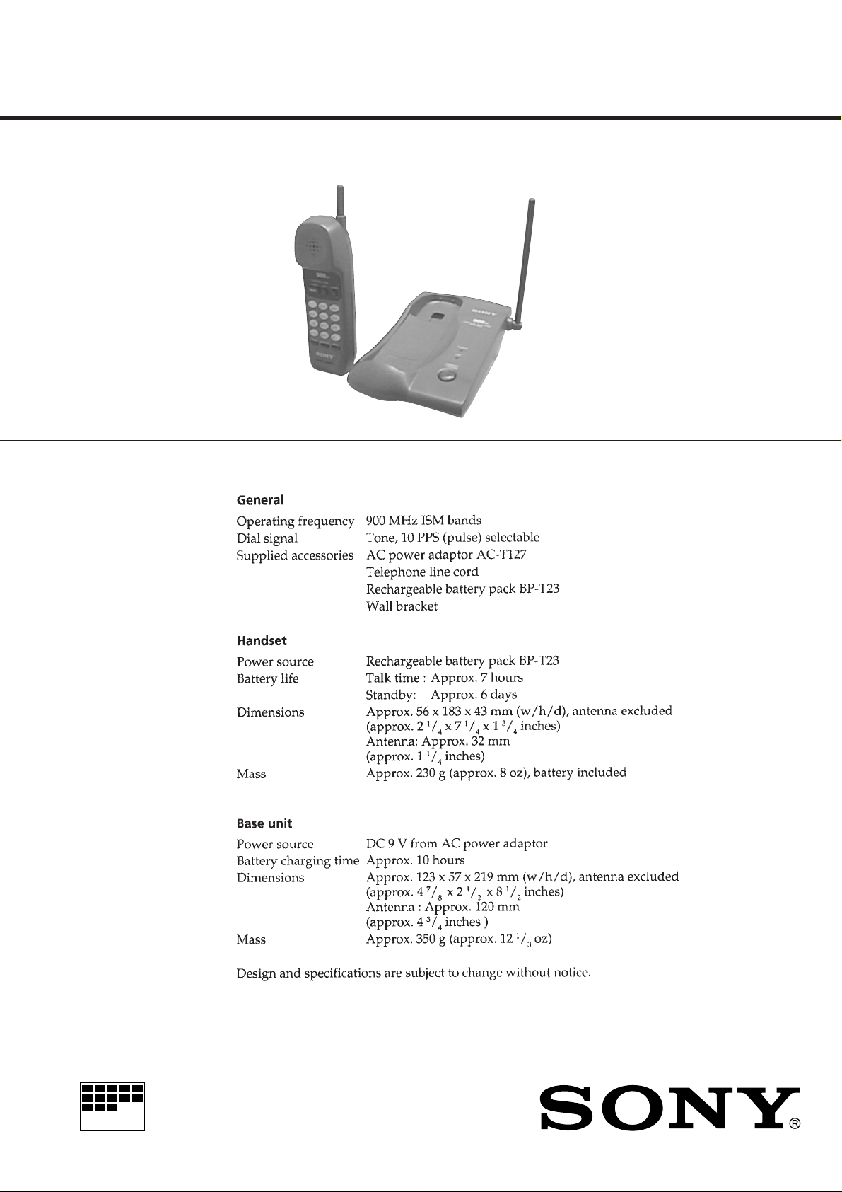
SPP-904
SERVICE MANUAL
SPECIFICATIONS
E Model
MICROFILM
CORDLESS TELEPHONE
Page 2

TABLE OF CONTENTS
1. GENERAL
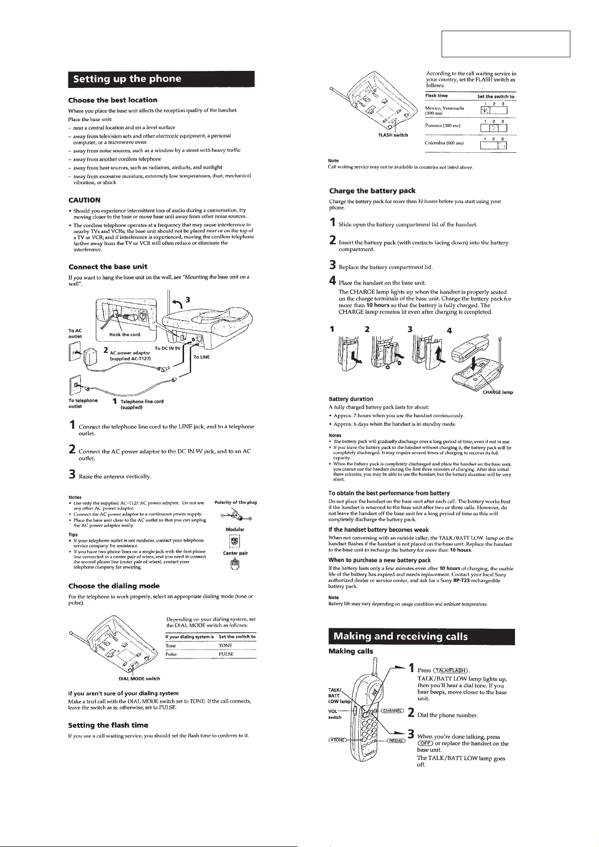
Setting Up the Phone ...................................................... 3
Making and Receiving Calls........................................... 3
2. DISASSEMBLY ......................................................... 5
3. TEST MODE.............................................................. 7
4. ELECTRICAL ADJUSTMENTS
Base Unit ......................................................................... 10
Handset ............................................................................ 13
5. DIAGRAMS
5-1. Block Diagram – BASE UNIT Section –...................... 17
5-2. Block Diagram – HANDSET Section –........................ 18
5-3. Note for Printed Wiring Boards and
Schematic Diagrams ....................................................... 19
5-4. Printed Wiring Board – BASE RF Section – ................ 20
5-5. Schematic Diagram – BASE RF Section – ................... 21
5-6. Printed Wiring Board – BASE MAIN Section –........... 22
5-7. Schematic Diagram – BASE MAIN Section – ............. 23
5-8. Printed Wiring Board – HAND RF Section –............... 24
5-9. Schematic Diagram – HAND RF Section – .................. 25
5-10. Printed Wiring Board – HAND MAIN Section – ........ 26
5-11. Schematic Diagram – HAND MAIN Section – ............ 27
5-12. IC Pin Function Description ........................................... 29
Notes on chip component replacement
• Never reuse a disconnected chip component.
• Notice that the minus side of a tantalum capacitor may be damaged by heat.
SAFETY-RELATED COMPONENT WARNING!!
COMPONENTS IDENTIFIED BY MARK 0 OR DOTTED
LINE WITH MARK 0 ON THE SCHEMATIC DIAGRAMS
AND IN THE PARTS LIST ARE CRITICAL TO SAFE
OPERATION. REPLACE THESE COMPONENTS WITH
SONY PARTS WHOSE PART NUMBERS APPEAR AS
SHOWN IN THIS MANU AL OR IN SUPPLEMENTS PUBLISHED BY SONY.
6. EXPLODED VIEWS ................................................ 31
7. ELECTRICAL PARTS LIST ............................... 33
2
Page 3
SECTION 1
GENERAL
This section is extracted from
instruction manual.
3
Page 4
4
Page 5
SECTION 2
d
)
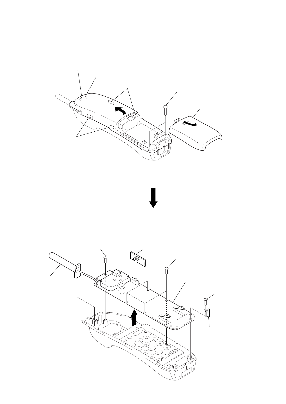
DISASSEMBLY
Note: Follow the disassembly procedure in the numerical order given.
HAND CABINET (REAR)
5
Remove the hand cabinet (rear)
to direction of the arrow B.
4
claw
3
two claws
B
3
two claws
2
two screws
(BTP2.6 × 12)
A
1
Remove the battery case li
to direction of the arrow A.
HAND MAIN BOARD
6
antenna cover
2
screw
(BTP2.6
×
8)
1
C
vol knob (U)
2
four screws
(BTP2.6
×
8)
5
Remove the hand main board
to direction of the arrow
3
two screws
(BTP2
4
two charge terminals (U
C
.
×
6)
5
Page 6
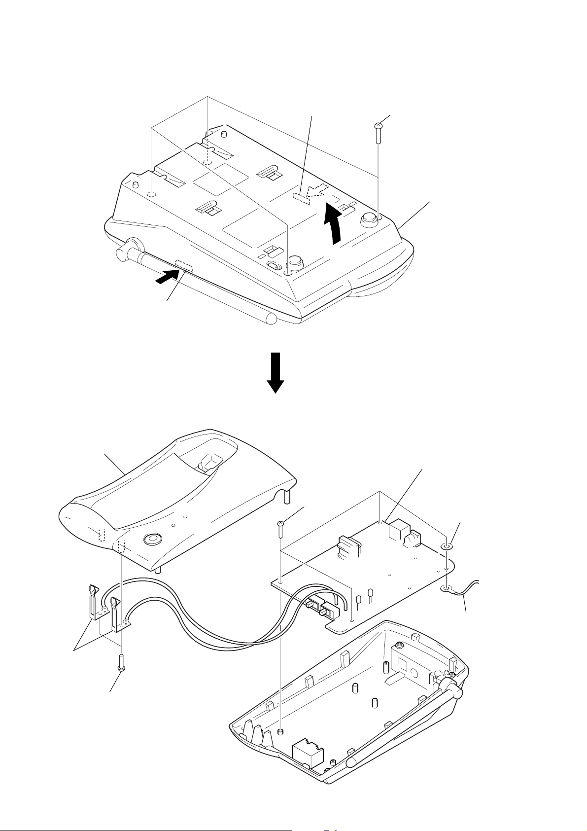
BASE CABINET
2
claw
2
claw
1
four screws
(BTP2.6
×
10)
3
cabinet (lower)
BASE MAIN BOARD
3
cabinet (upper)
2
two charge
springs (U)
1
two screws
(BTP2.6
6
base main board
4
four screws
(BTP2.6
×
8)
×
8)
5
washer (SP)
7
harness
6
Page 7

SECTION 3
TEST MODE
BASE UNIT
[Setting the Test Mode]
1. Power on with pressing the [HANDSET LOCATOR] key for two seconds.
2. CHARGE and LINE LEDs turn on for 50 msec, and the test mode is set.
* If setting the test mode with the status that [TONE] position is selected at [DIAL MODE] switch, the unit cold stars next time when the
power is turned on.
[Releasing the Test Mode]
To release the test mode, perform as follows:
• Turn the power off (disconnect the AC adapter plug).
• Set the handset to charge on the base unit (except Test Mode 9).
• Bell in.
[Changing the Test Mode Step]
1. Set the [DIAL MODE] switch to the [PULSE] position.
2. Press the [HANDSET LOCATOR] key.
3. A step is changed each time the key is pressed, and CHARGE and LINE LEDs turn on for 50 msec.
[Changing the Channel]
1. Set the [DIAL MODE] switch to the [TONE] position.
2. Press the [HANDSET LOCATOR] key.
3. A channel is changed each time the key is pressed, and CHARGE and LINE LEDs turn on for 50 msec.
* Channel will be back to initial channel (19CH), when the test mode step is changed.
• Channel Rotation
21CH 40CH 1CH 2CH 3CH 39CH 40CH20CH19CH
. . .
7
Page 8
[Test Mode Execution]
Press the [HANDSET LOCATOR] key to execute any of the following tests:
Step
1 VCO/TX FREQ. ADJ L L L L
2 TX MOD CHECK L H L H
3 TX DATA L L L L *1
4 RX SENS H L H H
5 SQ SENS L L *A H
6 DTMF SINGLE TONE H L L H *2
7 DTMF DUAL TONE H L L H *3
8 DATA IN CHECK L L L L *4
9 CHARGE CHECK H L L L *5
10 DUPLEX L H H H
Test Mode
Name
Remarks
TALK (IC5 pin qd)
RX MUTE (IC5 pin eh)
TX MUTE (IC5 pin ej)
TX (IC5 pin rh)
* Initial Channel of each step: 19CH
*A. SQ on: H (CHARGE LED turns on)
SQ off: L (CHARGE LED turns off)
*1. Test Mode 3: Continue output TX data as “ 0000……”.
*2. Test Mode 6: Set the
[DIAL MODE] switch to the [TONE] position, and press the [HANDSET LOCATOR] key.
DTMF will be changed.
ROW 1 → ROW 2 → ROW 3 → ROW 4 → COL1 → COL2 → COL3 → ROW1 → …… .
*DTMF frequency
ROW 1: 696.95 Hz COL1: 1209.31 Hz
ROW 2: 770.13 Hz COL2: 1335.65 Hz
ROW 3: 852.27 Hz COL3: 1476.71 Hz
ROW 4: 940.99 Hz
*3. Test Mode 7: Set the [DIAL MODE] switch to the [TONE] position, and press the [HANDSET LOCATOR] key.
DTMF will be changed.
1 → 2 → 3 → 4 → 5 → 6 → 7 → 8 → 9 → 0 → → # → 1 → …… .
*
*4. Test Mode 8: When locked receiving data is “ 0000……”, CHARGE LED turns on.
*5. Test Mode 9: When CHGIN (IC5 pin eg) is “ L” (charge on), CHARGE LED turns on.
8
Page 9
HANDSET
[Setting the Test Mode]
1. Power on with press the [*] key and the [#] key simultaneously for one second.
2. It beeps confirm tone, and the test mode is set.
* If the [PGM] key is pressed, the unit cold starts next time when the power is turned on.
[Releasing the Test Mode]
To release the test mode, perform as follows:
• Press the [FLASH, TALK] key.
• Turn the power off (remove the battery pack).
• Set the handset to charge on the base unit (except Test Mode 9).
[Changing the Test Mode Step]
Press the each key of the test mode step number.
[Changing the Channel]
Press the [CHANNEL] key.
* The channel is back to initial channel (6CH), when test mode step is changed.
• Channel Rotation
19CH 40CH 1CH 2CH 3CH 39CH 40CH20CH21CH
[Test Mode Execution]
Press the each key for the desired test mode step to execute any of the following tests:
No.
1 VCO/TX FREQ. ADJ 1 L H L L L
2 TX MOD CHECK 2 L H H L H
3 TX DATA 3 L H L L H *1
4 RX SENS 4 H H L H H *2
5 SQ SENS 5 L H L *A H
6 RECEIVE DATA CHECK 6 L H L L H *3
7 BELL CHECK 7 H L L L H
8 BAT. LOW CHECK 8 H L L L H *4
9 CHARGE CHECK 9 H L L L H *5
10 DUPLEX 0 L H H H L *2
Test Mode
Name
KEY
RX PWR (IC404 pin qd)
TX B (IC404 pin rs)
TX MUTE (IC404 pin qa)
CONV (IC404 pin ej)
RX MUTE (IC404 pin qs)
* Initial Channel of each step: 21CH
. . .
Remarks
*A. SQ on: H
SQ off: L
*1. Test Mode 3: Continue output TX data as “ 0000……”.
*2. Test Mode 4, 10: It is possible to change the speaker output level by [VOL] switch.
*3. Test Mode 6: When locked receiving data is “ 0000……”, it beeps confirm tone. (1 kHz)
*4. Test Mode 8: When BATT LOW (IC404 pin eg) is “ L” (battery low), it beeps confirm tone.
*5. Test Mode 9: When CHG IN (IC404 pin eh) is “ L” (charge on), it beeps confirm tone.
9
Page 10
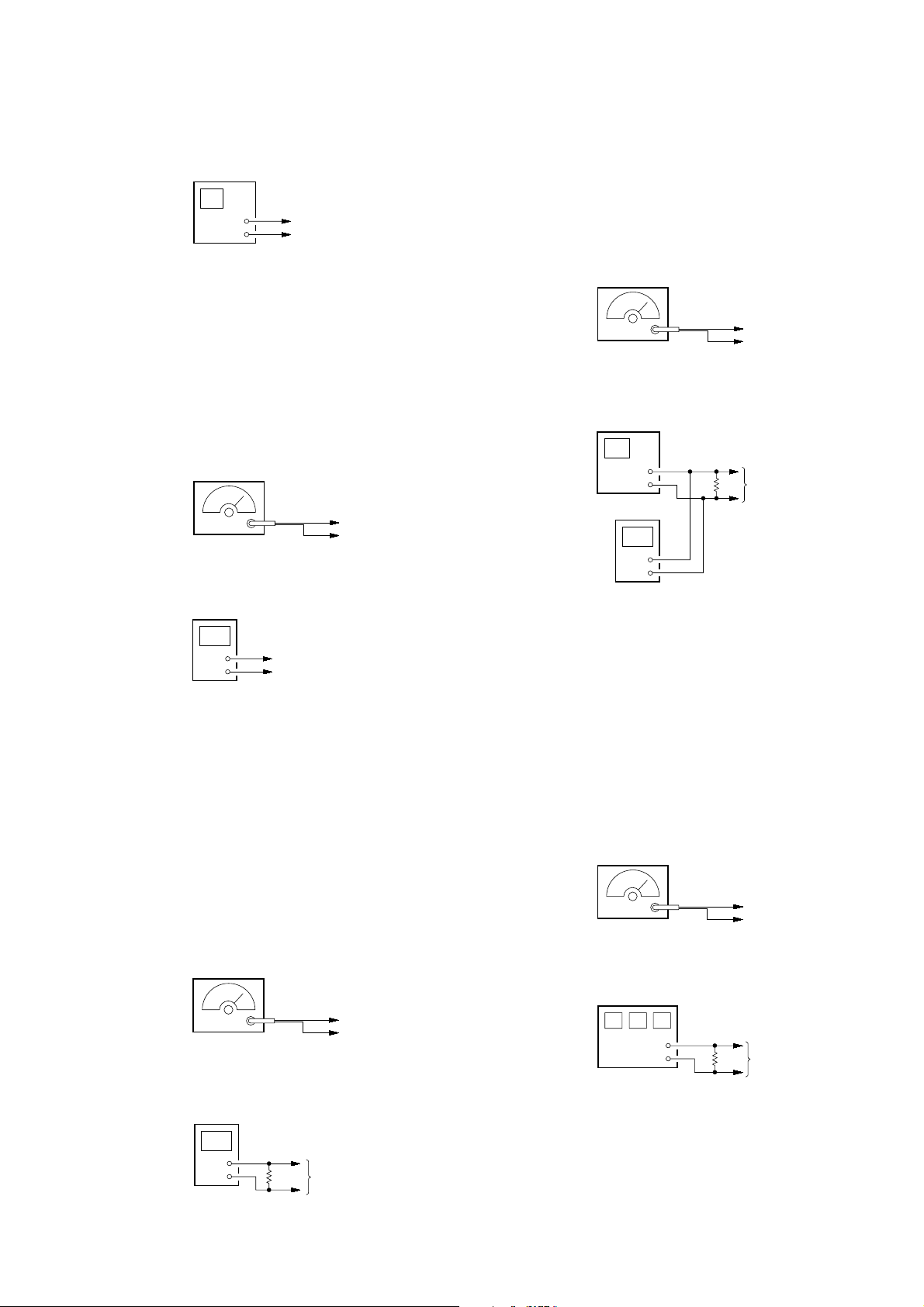
SECTION 4
+
–
deviation meter
TP (ANT)
TP (GND)
ELECTRICAL ADJUSTMENTS
0 dBm = 0.775 V
BASE UNIT
• Make the set in test mode. (See page 7.)
– TX Adjustments and Checks –
1. TX VCO Check
Setting:
digital voltmeter
+
–
Procedure:
1. Connect a digital voltmeter to TP (TX VCO), TP (RX VCO)
and TP (GND) on the BASE RF board.
2. Check that both TP (TX VCO) and TP (RX VCO) voltage of
digital voltmeter are 0.8 V to 2.2 V.
3. Set the
[DIAL MODE] switch (S2) to the [TONE] position.
4. Press the [HANDSET LOCATOR] key (S1) three times to change
the channel to 40CH.
5. Check that both TP (TX VCO) and TP (RX VCO) voltage of
digital voltmeter are 0.8 V to 2.2 V.
6. Press the [HANDSET LOCATOR] key (S1) once to change
the channel to 1CH.
7. Check that both TP (TX VCO) and TP (RX VCO) voltage of
digital voltmeter are 0.8 V to 2.2 V.
TP (TX VCO), TP (RX VCO)
TP (GND)
7. Check that the value of power meter is –5.5 dBm ± 1.5 dBm.
4. Modulation Sensitivity Adjustment
Setting:
AF OSC
600
+
–
1 kHz, –20 dBm
Ω
LINE jack (J1)
Procedure:
1. Connect an AF OSC to the LINE jack (J1) on the B ASE MAIN
board.
2. Connect a de viation meter to TP (ANT) and TP (GND) on the
BASE MAIN board.
3. Set the [DIAL MODE] switch (S2) to the [PULSE] position.
4. Press the [HANDSET LOCATOR] key (S1) once to change
the test mode step to TX MOD CHECK.
5. Adjust RT3 on the BASE MAIN board so that the value of
deviation meter becomes 8 kHz ± 0.5 kHz.
5. Distortion and S/N Ratio Check
Setting:
2. TX Frequency Adjustment
Setting:
frequency counter
+
–
TP (ANT)
TP (GND)
Procedure:
1. Connect a frequency counter to TP (ANT) and TP (GND) on
the BASE MAIN board.
2. Restart the test mode to change the channel to 19CH.
3. Adjust CT1 on the BASE MAIN board so that the value of
frequency counter becomes 926.897468 MHz ± 600 Hz.
3. TX Power Adjustment
Setting:
power meter
+
–
TP (ANT)
TP (GND)
Procedure:
1. Connect a power meter to TP (ANT) and TP (GND) on the
BASE MAIN board.
2. Adjust R T301 on the B ASE RF board so that the value of pow er
meter becomes –5.5 dBm ± 1 dBm.
3. Set the
[DIAL MODE] switch (S2) to the [TONE] position.
4. Press the [HANDSET LOCATOR] key (S1) three times to change
the channel to 40CH.
5. Check that the value of power meter is –5.5 dBm ± 1.5 dBm.
6. Press the [HANDSET LOCATOR] key (S1) once to change
the channel to 1CH.
AF OSC
600
+
–
1 kHz, –20 dBm
distortion meter
noise meter
CCITT: on
Ω
LINE jack (J1)
+
–
+
–
TP (ANT)
TP (GND)
Procedure:
1. Connect a distortion meter and noise meter to TP (ANT) and
TP (GND) on the BASE MAIN board.
2. Check that the value of distortion meter is less than 4%.
3. Check that the value of noise meter, and record it.
4. Stop outputting the signal of AF OSC.
5. Check that the v alue of noise meter again. And check that difference of level between in step3 and in step5 is less than
30 dB.
10
Page 11
6. Code Deviation Check
600
Ω
+
–
SINAD meter
LINE jack (J1)
Setting:
deviation meter
+
–
TP (ANT)
TP (GND)
Procedure:
1. Connect a de viation meter to TP (ANT) and TP (GND) on the
BASE MAIN board.
2. Press the [HANDSET LOCATOR] key (S1) once to change
the test mode step to TX DATA.
3. Check that the value of deviation meter is 6 kHz to 10 kHz.
– RX Adjustments and Checks –
1. DISCRI Volta ge Adjustment
Setting:
SSG
TP (ANT)
Carrier frequency: 902.952467 MHz
Modulation: no modulation
Output level: – 47 dBm
digital voltmeter
TP (GND)
Procedure:
1. Change the modulation of SSG to 1 kHz, ± 8 kHz deviation.
2. Connect a noise meter to the LINE jack (J1) on the BASE
MAIN board.
3. Adjust RT2 on the BASE MAIN board so that the value of
noise meter becomes 265 mV ± 10 mV.
3. Distortion and S/N Ratio Check
Setting:
SSG
TP (ANT)
Carrier frequency: 902.952467 MHz
Modulation: 1 kHz,
Output level: – 47 dBm
distortion meter
±
8 kHz deviation
+
–
noise meter
+
–
CCITT: on
600
TP (GND)
Ω
LINE jack (J1)
+
–
TP (DISCRI)
TP (GND)
Procedure:
1. Connect a SSG to TP (ANT) and TP (GND) on the BASE
MAIN board.
2. Connect a digital v oltmeter to TP (DISCRI) and TP (GND) on
the BASE MAIN board.
3. Set the
[DIAL MODE] switch (S2) to the [PULSE] position.
4. Press the [HANDSET LOCATOR] key (S1) three times to change
the test mode step to RX SENS.
5. Adjust L3 on the B ASE MAIN board so tha t the value of digital voltmeter becomes 1 V ± 0.05 V.
2. TEL Out Level Adjustment
Setting:
SSG
TP (ANT)
Carrier frequency: 902.952467 MHz
Modulation: 1 kHz,
Output level: – 47 dBm
±
8 kHz deviation
TP (GND)
Procedure:
1. Connect a distortion meter to the LINE jack (J1) on the B ASE
MAIN board.
2. Set the CCITT of noise meter on.
3. Check that the value of distortion meter is less than 4%.
4. Check that the value of noise meter, and record it.
5. Change the modulation of SSG to no modulation.
6. Check that the v alue of noise meter again. And check that difference of level between in step3 and in step5 is more than
60 dB.
4. RX Sensitivity Check
Setting:
SSG
TP (ANT)
Carrier frequency: 902.952467 MHz
Modulation: 1 kHz,
Output level: –111 dBm
±
8 kHz deviation
TP (GND)
noise meter
+
–
600
Ω
LINE jack (J1)
Procedure:
1. Connect a SINAD meter to the LINE jack (J1) on the BASE
MAIN board.
2. Change the output level of SSG to –111 dBm, and change the
modulation to 1 kHz ± 8 kHz devition.
3. Check that the value of SINAD meter is more than 12 dB.
11
Page 12
5. SQ Sensitivity Adjustment
Setting:
6. DTMF Level Check
Setting:
SSG
Carrier frequency: 902.952467 MHz
Modulation: 1 kHz, ±8 kHz deviation
Output level: –113 dBm
TP (ANT)
TP (GND)
noise meter
+
–
600
Ω
LINE jack (J1)
Procedure:
1. Connect a noise meter to the LINE jack (J1) on the BASE
Procedure:
1. Change the output level of SSG to –113 dBm.
2. Press the [HANDSET LOCATOR] key (S1) once to change
the test mode step to SQ SENS.
MAIN board.
2. Press the [HANDSET LOCATOR] key (S1) twice to change
the test mode step to DTMF DUAL TONE.
3. Check that the value of noise meter is –5 dBm to 0 dBm.
3. Adjust RT1 so that the CHARGE LED (D6) becomes blinking.
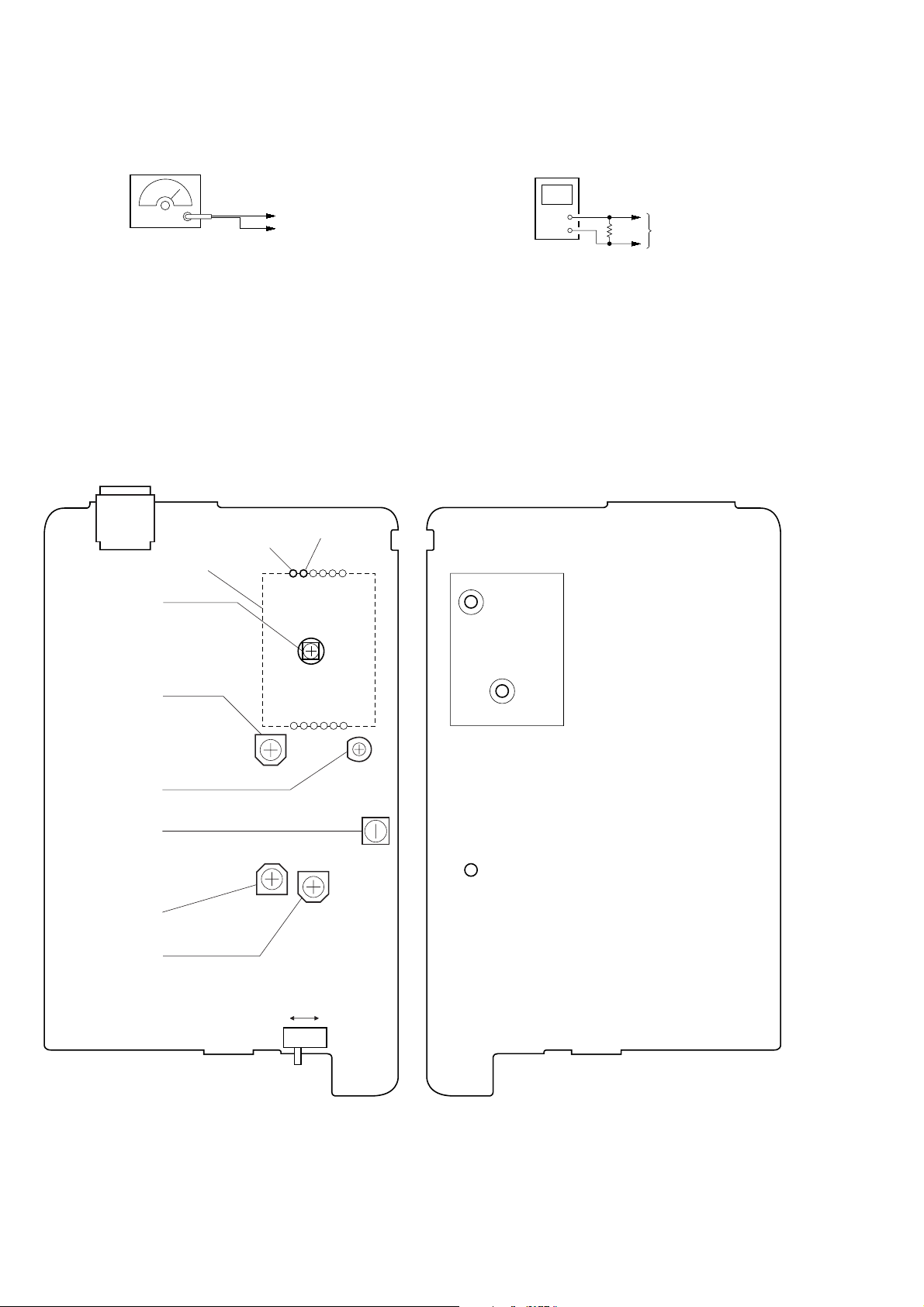
Adjustment Location:
– BASE MAIN BOARD (Component Side) – – BASE MAIN BOARD (Conductor Side) –
J1
TP(ANT)
BASE RF Board BASE RF Board
RT301
TX Power Adjustment
TP(GND)
TP(RX VCO)
Modulation Sensitivity
RT3
Adjustment
CT1
TX Frequency Adjustment
L3
DISCRI Voltage Adjustment
RT2
TEL Out Level Adjustment
RT1
SQ Sensitivity Adjustment
TP(TX VCO)
TP(DISCRI)
TONE PULSE
S2
12
Page 13

HANDSET
TP (MIC+)
TP (MIC–)
AF OSC
1 kHz, 9 mV
+
–
• Make the set in test mode. (See page 9.)
– TX Adjustments and Checks –
4. Modulation Sensitivity Adjustment
Setting:
AF OSC
1. TX VCO Check
Setting:
digital voltmeter
+
–
TP (TX VCO), TP (RX VCO)
TP (GND)
Procedure:
1. Connect a digital voltmeter to TP (TX VCO), TP (RX VCO)
and TP (GND) on the HAND RF board.
2. Check that both TP (TX VCO) and TP (RX VCO) voltage of
digital voltmeter are 0.8 V to 2.2 V.
3. Press the [CHANNEL] key three times to change the channel
to 40CH.
4. Check that both TP (TX VCO) and TP (RX VCO) voltage of
digital voltmeter are 0.8 V to 2.2 V.
5. Press the [CHANNEL] key once to change the channel to 1CH.
6. Check that both TP (TX VCO) and TP (RX VCO) voltage of
digital voltmeter are 0.8 V to 2.2 V.
2. TX Frequency Adjustment
Setting:
frequency counter
+
–
TP (MIC+)
TP (MIC–)
TP (ANT)
TP (GND)
+
–
1 kHz, 9 mV
deviation meter
Procedure:
1. Disconnect the microphone (MC401).
2. Connect an AF OSC to TP (MIC+) and TP (MIC–) on the
HAND MAIN board.
3. Connect a de viation meter to TP (ANT) and TP (GND) on the
HAND MAIN board.
4. Press the [2] key to change the test mode step to TX MOD
CHECK.
5. Adjust RT403 on the HAND MAIN board so that the value of
deviation meter becomes 8 kHz ± 0.5 kHz.
5. Distortion and S/N Ratio Check
Setting:
+
–
TP (ANT)
TP (GND)
Procedure:
1. Connect a frequency counter to TP (ANT) and TP (GND) on
the HAND MAIN board.
2. Restart the test mode to change the channel to 21CH.
3. Adjust CT401 on the HAND MAIN board so that the v alue of
frequency counter becomes 903.052467 MHz ± 600 Hz.
3. TX Power Adjustment
Setting:
power meter
+
–
TP (ANT)
TP (GND)
Procedure:
1. Connect a power meter to TP (ANT) and TP (GND) on the
HAND MAIN board.
2. Adjust RT501 on the HAND RF board so that the value of
power meter becomes –7.5 dBm ± 1 dBm.
3. Press the [CHANNEL] key three times to change the channel
to 40CH.
4. Check that the value of power meter is –7.5 dBm ± 1.5 dBm.
5. Press the [CHANNEL] key once to change the channel to 1CH.
6. Check that the value of power meter is –7.5 dBm ± 1.5 dBm.
distortion meter
+
–
noise meter
+
–
CCITT: on
TP (ANT)
TP (GND)
Procedure:
1. Connect a distortion meter and noise meter to TP (ANT) and
TP (GND) on the HAND MAIN board.
2. Check that the value of distortion meter is less than 4%.
3. Check that the value of noise meter, and record it.
4. Stop outputting the signal of AF OSC.
5. Check that the v alue of noise meter again. And check that difference of level between in step3 and in step5 is less than
30 dB.
13
Page 14

6. Code Deviation Check
Setting:
deviation meter
+
–
TP (ANT)
TP (GND)
4. Set the [VOL] switch (S401) to [M] position.
5. Adjust RT402 on the HAND MAIN board so that the value of
noise meter becomes 115 mV ± 10 mV.
3. Distortion and S/N Ratio Check
Setting:
SSG
Procedure:
1. Connect a de viation meter to TP (ANT) and TP (GND) on the
HAND MAIN board.
2. Press the [3] key to change the test mode step to TX DATA.
3. Check that the value of deviation meter is 6 kHz to 10 kHz.
– RX Adjustments and Checks –
1. DISCRI V oltage Adjustment
Setting:
SSG
TP (ANT)
Carrier frequency: 926.997467 MHz
Modulation: no modulation
Output level: – 47 dBm
digital voltmeter
+
–
TP (DISCRI)
TP (GND)
TP (GND)
Procedure:
1. Connect a SSG to TP (ANT) and TP (GND) on the HAND
MAIN board.
2. Connect a digital v oltmeter to TP (DISCRI) and TP (GND) on
the HAND MAIN board.
3. Press the
[4] key to change the test mode step to RX SENS.
4. Adjust L402 on the HAND MAIN board so that the value of
digital voltmeter becomes 1 V ± 0.05 V.
2. Speaker Out Level Adjustment
Setting:
SSG
TP (ANT)
Ω
TP (GND)
TP (SP+)
TP (SP–)
Carrier frequency: 926.997467 MHz
Modulation: 1 kHz,
Output level: – 47 dBm
distortion meter
±
8 kHz deviation
+
–
noise meter
+
–
CCITT: on
150
Procedure:
1. Connect a distortion meter to TP (SP+) and TP (SP–) on the
HAND MAIN board.
2. Check that the value of distortion meter is less than 4%.
3. Check that the value of noise meter, and record it.
4. Change the modulation of SSG to no modulation.
5. Check that the v alue of noise meter again. And check that difference of level between in step3 and in step5 is more than
60 dB.
4. RX Sensitivity Check
Setting:
SSG
TP (ANT)
Carrier frequency: 926.997467 MHz
Modulation: 1 kHz,
Output level: –111 dBm
SINAD meter
±
8 kHz deviation
TP (GND)
TP (ANT)
Carrier frequency: 926.997467 MHz
Modulation: 1 kHz, ±8 kHz deviation
Output level: – 47 dBm
noise meter
150
+
–
Ω
TP (GND)
TP (SP+)
TP (SP–)
Procedure:
1. Change the modulation of SSG to 1 kHz, ± 8 kHz deviation.
2. Disconnect the speaker (SP801).
3. Connect a noise meter to TP (SP+) and TP (SP–) on the HAND
MAIN board.
14
150
+
–
Ω
TP (SP+)
TP (SP–)
Procedure:
1. Change the output level of SSG to –111 dBm.
2. Connect a SINAD meter to TP (SP+) and TP (SP–) on the
HAND MAIN board.
3. Check that the value of SINAD meter is more than 12 dB.
Page 15

5. SQ Sensitivity Adjustment
Setting:
SSG
TP (ANT)
Carrier frequency: 926.997467 MHz
Modulation: 1 kHz,
Output level: –113 dBm
±
8 kHz deviation
TP (GND)
Procedure:
1. Change the output level of SSG to –113 dBm.
2. Press the [5] key to change the test mode step to SQ SENS.
3. Adjust RT401 so that the TALK/BATT LOW LED (D408)
becomes blinking.
Adjustment Location:
RT501
TX Power
Adjustment
TP
(RX VCO)
CT401
TX Frequency
Adjustment
L402
DISCRI Voltage
Adjustment
RT402
Speaker Out Level
Adjustment
RT403
Modulation Sensitivity
Adjustment
– HAND MAIN BOARD –
(Component Side)
TP(SP–)
TP(SP+)
HAND RF Board
TP(TX VCO)
– HAND MAIN BOARD –
(Conductor Side)
TP(ANT)
TP(GND)
TP(DISCRI)
RT401
SQ Sensitivity
Adjustment
TP(MIC+)
TP(MIC–)
MC401
15
Page 16

16
Page 17

SECTION 5
DIAGRAMS
5-1. BLOCK DIAGRAM – BASE UNIT Section –
ANT1
(ANTENNA)
TX AMP
Q306, 307
2
RT301
TX
POWER
TX
OUT
RF AMP
Q301
B.P.F.
FT301
TX B+
SWITCH
Q302
2 DOUBLER
TX AMP
1st MIXER, VCO, PLL SYNTHESIZER
24
TX B+
14
MIX
IN
MIXER
LOCAL OSC
BUFFER
(RX SYSTEM)
LOCK
(TX SYSTEM)
IC302
1st
VCO
VCO
MIX
OUT
TXE
TXB
RXE
RXB
13
10.555MHz
20
21
5
4
FT1
RX VCO
Q312
TX
VCO
IF AMP
Q1
X2
10.1MHz
CT1
TX
FREQUENCY
L.P.F.
D303
LOCK
DETECTOR
L.P.F.
D302
2nd MIXER, LIMITER AMP, DET,
AF AMP, SQUELCH CONTROL
16
MIX
IN
18
7
2nd
MIXER
LOCAL
OSC
OSC
1 2
PD2
PD1
IC3
OSC
MIX
OUT
PHASE
DETECTOR
PHASE
DETECTOR
SPP-904
L3
DISCRI
VOLTAGE
FT2
455kHz
3
LIM
IN
5
PROGRAM-
MABLE
DIVIDER
LATCH
PROGRAM-
MABLE
DIVIDER
LATCH
LIMITER
AMP
SQUELCH
TRIGGER
WITH
HYSTERESIS
SCAN
CONTROL
13
QUAD COIL
MODULATOR
12
1/32, 1/33
PRESCALER
1/16, 1/17
PRESCALER
DE-
B+ (+3V)
EXPANDER, COMPRESSOR, LIMITER
8
AF
OUT
AF
9
FIL
INSQ IN
1011
RT3
MODULATION
SENSITIVITY
FIL
OUT
AMP
FILTER
AMP
RT2
TEL
OUT LEVEL
RT1
SQ
SENSITIVITY
47 48
39
SQ IN
DATA EN
DATA OUT
SYSTEM CONTROLLER
IC5
PREAMP
COMP
OUT
20
TX MUTE
RX MUTE
DATA IN
DTMF
DTMF
TALK
BELL IN
EXP
IN
Q2
LIMITER
37
36
38
1
34
13
21
3
LPF1
IN
1
MUTE
CMP MUTE
CONT
EXP MUTE
EXPANDER
VCA
L.P.F.
COMPRESSOR
CONT
1617
IC1
VCA
SUM
AMP
DATA
SHAPE
SUM
AMP
MUTE
DRIVE
TEL
OUT
FSK
OUT
PRE
AMP
6
10
PRE
IN
+
24
HOOK ON/OFF
RELAY DRIVE
Q10
RINGER DETECT
IC4
LPF2
IN
19
L.P.F.
AF AMP
Q4
LPF2
OUT
RL1
18
HYBRID
AMP
Q3
T1
LINE
TRANSFORMER
J1
LINE
• SIGNAL PATH
: RX
: TX
: BELL
05
1/2
SHIFT
XIN
9
XOUT
10
SI
16
CPS
15
17
RST
S1
PULSE
TONE
1
2
3
41
PLL DATA
40
PLL CLK
42
PLL EN
20
PAGE
22
TONE/PULSE
FLASH 100
24
23
FLASH 270
LED CHG1
LED CHG2
LED INUSE1
LED INUSE2
X0
5
BATT OFF
RESET
TX B
CHG OUT
CHG IN
X1
6
32
31
30
29
18
2
46
25
35
PROGRAM-
MABLE
DIVIDER
LATCH
OSC &
1/2 DIVIDER
REGISTER &
LATCH
PULSE
COUNTER
HANDSET
LOCATOR
S2
DIAL MODE
S3
FLASH
D6
CHARGE
D7
LINE
RESET SIGNAL
GENERATOR
Q9
B+ (+3V)
BATTERY
VOLTAGE DETECT
IC6
B+ (+3V)
TX B+ (+3V)
B+ SWITCH
(FOR TX SYSTEM)
Q12
REGULATOR
CHARGE CONTROL
Q8
CHARGE DETECT
Q6
+3V
Q11
B+ (+6V)
+6V
REGULATOR
Q7
J2
!
DC IN 9V
+
–
CHARGE
TERMINAL
X1
3.579545MHz
1717
Page 18

SPP-904
5-2. BLOCK DIAGRAM – HANDSET Section –
ANT2
(ANTENNA)
TX AMP
Q506, 507
RT501
TX
POWER
RF AMP
Q501
B.P.F.
FT501
SWITCH
1st MIXER, VCO, PLL SYNTHESIZER
24
TX B+
TX B+
Q502
14
MIX
IN
MIXER
LOCAL OSC
BUFFER
(RX SYSTEM)
LOCK
IC502
1st
VCO
MIX
OUT
RXE
RXB
13
10.555MHz
20
21
FT401
RX VCO
Q512
IF AMP
Q401
X401
10.1MHz
CT401
TX
FREQUENCY
L.P.F.
D503
LOCK
DETECTOR
2nd MIXER, LIMITER AMP, DET,
AF AMP, SQUELCH CONTROL
IC401
MIX
IN
16
18
2nd
MIXER
LOCAL
OSC
OSC
1 2
PD2
OSC
MIX
OUT
PHASE
DETECTOR
L402
DISCRI
VOLTAGE
FT402
455kHz
3
LIM
IN
5
PROGRAM-
MABLE
DIVIDER
LATCH
LIMITER
AMP
SQUELCH
TRIGGER
WITH
HYSTERESIS
SCAN
CONTROL
13
QUAD COIL
MODULATOR
12
1/32, 1/33
PRESCALER
DE-
B+ (+3V)
8
AF
OUT
FIL
OUT
AF
AMP
FILTER
AMP
9
FIL
INSQ IN
1011
RT403
MODULATION
SENSITIVITY
RT402
SPEAKER
OUT LEVEL
RT401
SQ
SENSITIVITY
44 45
41
SQ IN
DATA OUT
SYSTEM CONTROLLER
IC404
PREAMP
DATA EN
TX MUTE
RX MUTE
DATA IN
CONV
Q402
20
COMP
OUT
11
12
40
37
EXPANDER, COMPRESSOR, LIMITER
EXP
IN
3
LPF1
IN
1
LIMITER
EXPANDER
VCA
L.P.F.
MUTE
CMP MUTE
CONT
IC403
EXP MUTE
CONT
1617
SUM
AMP
DATA
SHAPE
COMPRESSOR
VCA
MUTE
DRIVE
SUM
AMP
INT
OUT
FSK
OUT
S401
VOL
H/M/L
VOLUME
5
CONTROL
S401
VREF B+
10
PRE
IN
PRE
AMP
24
LPF2
IN
19
VREF
14 13
L.P.F.
REG.
LPF2
OUT
VCC
ST.BY.
18
12
MIC AMP
Q404
B+ (+3V)
STANDBY
SWITCH
Q412
AF AMP
Q405, 406
SP801
(SPEAKER)
MC401
(MIC)
TX
OUT
2
2 DOUBLER
TX AMP
• SIGNAL PATH
: RX
: TX
: BELL
05
VCO
(TX SYSTEM)
TXE
TXB
D408
RINGER DRIVE
Q408
(KEY BACK LIGHT)
BATT B+
D421 – 424
B+ (+3V)
TX B+ (+3V)
PROGRAM-
5
4
TX
VCO
L.P.F.
D502
PD1
7
PHASE
DETECTOR
1/2
MABLE
DIVIDER
LATCH
PROGRAM-
MABLE
DIVIDER
LATCH
1/16, 1/17
PRESCALER
OSC &
1/2 DIVIDER
SHIFT
REGISTER &
LATCH
PULSE
COUNTER
XIN
XOUT
CPS
SI
RST
9
10
16
15
17
47
46
48
PLL DATA
PLL CLK
PLL EN
RING OUT
RING VOL
KEY LED
TALK LED
TALK LED
TX B
CHG IN
38
RINGER VOLUME
39
17
16
15
42
13
SC
36
SWITCH
Q409
LED DRIVE
Q421
TALK/BATT LOW
Y401
(BUZZER)
SYSTEM CONTROLLER (IC404) B+
B+ SWITCH
(FOR TX SYSTEM)
Q403
CHARGE
DETECT
Q410
D407
+3V
REGULATOR
IC405
D406
BATT B+
D405
D403D404
BT901
RECHARGEABLE
BATTERY PACK
(BP-T23)
+
CHARGE
TERMINAL
–
KEY MATRIX
(SHEET KEY)
S901 – S918
ROW1 – ROW4
34 – 30 25 – 22
COL1 – COL5
BATT LOW
X0
5
BATT OFF
RESET
X1
6
35
29
2
RESET SIGNAL
GENERATOR
Q411
VDET1
1
VDET2
5
BATTERY
VOLTAGE DETECT
IC406
COMPARATOR
COMPARATOR
VREF
VIN1
VIN2
2
4
BATT B+
X402
3.579545MHz
1818
Page 19

5-3. NOTE FOR PRINTED WIRING BOARDS AND SCHEMATIC DIAGRAMS
Note on Printed Wiring Board:
• X : parts extracted from the component side.
• Y : parts extracted from the conductor side.
• W : indicates side identified with part number.
f
•
: internal component.
• b : Pattern from the side which enables seeing.
(The other layers' patterns are not indicated.)
• : carbon pattern
Caution:
Pattern face side: Parts on the pattern f ace side seen from
(Conductor Side) the pattern face are indicated.
Parts face side: Parts on the par ts face side seen from
(Component Side) the parts face are indicated.
Note on Schematic Diagram:
• All capacitors are in µF unless otherwise noted. pF: µµF
50 WV or less are not indicated except for electrolytics
and tantalums.
• All resistors are in Ω and 1/
specified.
f
•
: internal component.
4
W or less unless otherwise
• 2 : nonflammable resistor.
• 4: printed coil.
• C : panel designation.
• U : B+ Line.
• H : adjustment for repair.
• Power voltages are dc 9 V and fed with regulated dc pow er
supply from external power voltage jac k (J2) on the BASE
MAIN board, dc 12 V and fed with regulated dc power
supply from modular jack (J1) on the BASE MAIN board
with 100 Ω in series, and dc 3.6 V and f ed with regulated
dc power supply from battery terminal on the HAND MAIN
board.
• Voltages and wav eforms are dc with respect to ground in
test mode.
• Voltages are taken with a VOM (Input impedance 10 MΩ).
Voltage variations may be noted due to normal production tolerances.
• Waveforms are taken with a oscilloscope.
Voltage variations may be noted due to normal production tolerances.
• Circled numbers refer to waveforms.
• Signal path.
N : RX
O : TX
P : BELL
19
Page 20

5-4. PRINTED WIRING BOARD – BASE RF Section –
1234 567
A
B
A
BASE MAIN
BOARD
(Page 22)
C
ANT
GND
VCC
LE
DATA
CLK
D
BASE RF BOARD
L310
C303
L303
C315
C301
L301
R302
C398
R304
C378
L351
(SHIELD CASE)
C337
+
C339
L307
C334
L352
BASE RF BOARD
(COMPONENT SIDE)
1
FT301
3
C304
C307
C306
R342
R361C309
Q312
C324
BCE
C323
C362
AK
D303
R309
TP
R307
(RX VCO)
R328
C338
(CONDUCTOR SIDE)
C336
6
4
E
C
L302
C320
R329
C314
C312
C302
Q301
C325
L351-357
C373
+
R333
L354
C351
C341
AK
D302
C360
R327
C358
(PRINTED COIL)
(SHIELD CASE)
R319
C353
+
C357
C350
R326
TP(TX VOC)
1-675-273-
L353
C367
11
(11)
MOD
TX
GND
LO
GND
IF
B
BASE MAIN
BOARD
(Page 22)
C375
B
C369
E
C364
C365
L355
C371
C372
R351
Q306
C376
L357
C366
C310
R352
BCE
L356
C368
R354
C374
Q307
BCE
C370
R353
C363
R348
Q302
BCE
R339
R330
C344
C333
R344
R321
R303
C390
R331
L304
R306
R340
E
R397
R398
R399
C335
F
G
CLK
DATA
LE
VCC
GND
ANT
L306
R305
R332
C380
C381
C321
C326
C327
R322
C308
C305
C319
PRINTED
(
C379
L350
COIL
C311
R341
C342
12
C397
R316
C340
C348
C346
C345
R317
1
C347
C383
R359
R320
C382
IF
GND
LO
GND
TX
MOD
13
IC302
24
C386
C343
RT301
(
H
• Semiconductor
Location
Ref. No. Location
D302 C-5
D303 C-3
IC302 F-4
Q301 B-3
Q302 C-4
Q306 A-4
Q307 B-4
Q312 C-3
20
C349
L309
1-657-273-
05
11
(11)
Page 21

5-5. SCHEMATIC DIAGRAM – BASE RF Section – • See page 28 for IC Block Diagram.
SPP-904
1
BASE MAIN
BOARD
(Page 23)
ANT
GND
BASE RF BOARD
L310
18nH
2.4
C306
0.5p
Q306
0.8
R354
18k
C371
0.01
3
1
FT301
2
L307
6.8nH
R302
L356
C368
47k
4p
TP301
TP302
C375
2p
C302
12p
L302
6.8nH
C304
33p
C376
4p
C315
2p
L303
5.6nH
2SC4095-R47
R351
100
C369
33p
C301
2p
C303
2p
L301
18nH
Q301
RF AMP
0.8
2.1
L355
2SC5065-Y
TX AMP
C374
8p
C372
100p
R304
220
4
6
B.P.F.
5
R342
150
IC302
1st MIXER, VCO,
PLL SYNTHESIZER
M64884FP-C60J
C373
6p
1.6
L357
R352
10
C364
C365
0.1
33p
C390
0.01
C308
2p
C305
7p
C307
33p
IC302
0.7
Q307
2SC5065-Y
TX AMP
C370
TX POWER
RT301
4.7K
5p
C325
33p
R303
C321
L350
C363
R353
0.001
C310
C366
33p
6.8
33p
1.7
7p
39k
B+
C326
0.01
C319
33p
24
IN
MIX
TX GND1
1
1.9
R348
0
R341
1k
C360
10
6.3V
R322
33
B+
3.2
23
MIX GND
TX OUT
2
2.9
C342
3p
C386
0.01
B+
Q312
2SC5065-Y
RX VCO
C320
0.001
B+
22
RX VCC
TX VCC
3
1.7
B+
R344
33
C343
82p
21
4
2.8
C327
3p
1.8
RXB
TXB
0.9
C345
15p
R317
390
20
5
R361
1.3
R329
390
RXE
TXE
C346
15p
33k
2
C324
5p
C323
5p
1.4
19
RX GND
TX GND2
6
1.1
C347
8p
L353
L309
39nH
18
7
C309
L306
12nH
3.2
PD2
PD1
3.2
C348
0.01
B+
5p
17
8
L354
L351
3.2
16
RST
VCC
2.9
B+
C350
15p
D302
1SV270
C349
4p
9
L352
SI
XIN
C340
33p
C334
5p
1SV314
0
15
10
C341
4p
C351
100p
D303
C335
C344
0.01
CPS
XOUT
3p
0
14
11
(TX VCO)
R326
10k
C367
0.01
3.2
LOCK
XBO
TP
13
12
R319
0
R359
1.5k
TP
(RX VCO)
R305
10k
C362
3p
C311
27p
R340
4.7k
MIX OUT
GND
R321
10k
C353
0.01
R309
10k
C336
C397
100p
0.0033
R333
1.2k
R320
100k
C358
0.01
R307
3.3k
C337
C338
0.0047
0.0022
R339
330k
Q302
2SA812(M)-M6A
TX B+
SWITCH
2.4
3.1
R316
0
R330
10
R327
1k
C357
6.8
10V
R328
4.7k
C339
0.22
35V
B+
3.2
R332
1k
B+
R331
27
L304
4.7µH
C312
0.01
R306
1k
C314
0.01
C333
33p
C383
100p
100p
C381
R398
100p
C380
C379
100p
C378
R399
1k
R397
1k
B+
33p
B+
1k
B+
C398
100p
B+
C382
100p
B+
TP303
TP304
TP305
TP306
TP312
TP311
TP310
TP309
TP308
TP307
VCC
LE
DATA
CLK
MOD
TX
GND
LO
GND
IF
(Page 23)
2
BASE MAIN
BOARD
3
BASE MAIN
BOARD
(Page 23)
B+
05
B+
B+
2121
Page 22

SPP-904
5-6. PRINTED WIRING BOARD – BASE MAIN Section –
• Semiconductor
Location
Ref. No. Location
D1 G-9
D3 A-5
D4 C-3
D6 G-10
D7 G-11
D9 D-4
D10 C-12
D11 D-6
D13 E-3
IC1 C-8
IC3 G-8
IC4 D-3
IC5 B-11
IC6 D-11
Q1 F-7
Q2 F-9
Q3 A-8
Q4 C-7
Q6 E-12
Q7 D-5
Q8 E-11
Q9 D-11
Q10 D-6
Q11 E-3
Q12 F-6
1
2
3
4
5
6 7 8 9 10 11 12 13
BASE MAIN BOARD
A
C23
C22
C81
B
C
J1
LINE
6
4
2
1
3
5
C80
R25
D4
R37
1
2
R24
J2
C55
+
Q11
IC4
43
D13
R59
R58
C45
C51
+
–
DC IN 9V
D
C50
E
R51
R50
R65
TP(ANT)
TP(GND)
ANT
GND
VCC
LE
DATA
CLK
R70
C72
F
G
ANT1
PRINTED
(
BP(ANT)
COIL
L6
L50
(
C73
C82
R49
MOUNTED ON THE CONDUCTOR
(
SIDE OF BASE MAIN BOARD
D3
D9
Q7
C56
+
BASE RF BOARD
(SHIELD CASE)
C39
R38
RL1
Q10
C49
R60
(
C52
MOD
TX
GND
LO
GND
IF
H
05
BCE
+
LINE
TRANSFORMER
R76
R75
C83
Q12
1
2
FT1
3
R81
T1
D11
BCE
CT1
RT3
R36
C54
R48
R69
C79
C62
C65
C99
C38
R33
ECB
C36
C24L2R28 C25
C68
R92
C66
C64
1
C77
4
R23
X2
FT2
Q4
+
R99
Q1
BCE
R26 C1
R61 C30
C67
5
C35
R47
R68
R40
C26
Q3
BCE
R90
R88
R18
R19
C19
R21
R22
R34
R17
C18
R20
+
C10
C71 R86
13
IC1
24
+
C32
C13
+
R91
R45
R30
C63
12
1
+
C42
R84
C74
C31
C44
C12
R15
C17C75
R13
R16
C41
R42
R46
+
C43
R11
R89
C20
+
C37
C61
R41
C14
C78
R87
+
C33
R97
R70
R53
C34R14
C46
R98
C59
+
2536
R72
C58
R74
R79
24
13
12
C60
R57
C48
R80
3
1
IC6
2
R56
R78
R64
R95
R96
R94
R93
D10
S3
FLASH
R66
37
IC5
48
1
R71
C47
R73
X1
C57
Q9
BCE
Q6
R52
1
8
R27
BCE
R62
R39
R67
R63
Q8
C11 R9
R54
Q2
R1
16
IC3
9
C27
R29
+
C28
BCE
R8
R10
R2
C2
+
R3
C3
R4
C4 C7
C5
R6
L3
C9
D1
TP(DISCRI)
RT2
BLK
R5
C8
C6
RT1
CHARGE
R43
R55
R77
R44
D7D6
LINE
RED
3
2
1
S2
DIAL MODE
TONE
PULSE
C53
S1
HANDSET
LOCATOR
1-675-272-
A
(Page 20)
BASE RF BOARD
BASE RF BOARD
B
(Page 20)
+
–
CHARGE TERMINAL
11
(11)
2222
Page 23

5-7. SCHEMATIC DIAGRAM – BASE MAIN Section – • See page 24 for Waveforms. • See page 28 for IC Block Diagrams.
SPP-904
BASE MAIN BOARD
1.9
2SC2714-Y
0.001
C68
47p
C62
39p
(Page 21)
3
BASE RF
BOARD
(Page 21)
1
BASE RF
BOARD
2
BASE RF
BOARD
(Page 21)
CHARGE
TERMINAL
J2
DC IN 9V
Q1
IF AMP
L2
3.9µH
R26
220k
C24
1
BPF
2
0.7
FT1
GND
GND
MOD
ANT1
ANT
GND
VCC
DATA
CLK
C25
0.01
IF
LO
TX
LE
05
3
R1
680
0
R28
0
TP
(MOD)
B+
B+
R54
1k
10.1MHz
C77
FREQUENCY
R92
2.2k
R81
0
B+
L6
3.9nH
(ANT)
C73
2p
TP
7p
C1
33p
R2
18k
R27
470
3.2
IN
MIX
GND
OSC1
3.2 3.22.7 2.6 3.2 2.8 2.8 2.8
1
B+
X2
C66
100p
C64
0.01
CT1
C67
10p
3.2
BP
C70
100p
C53
2SA812
C79
0.0022
B+
2.4
Q12
L50
C72
0.001
100p
B+
C82
4p
C50
0.047
TP
(GND)
C65
15p
RT3
20K
(ANT)
CT1
TX
3.2
0.022
D1
1N4148
C2
2.2
50V
3.1 0.5 0.7 0.7
141516 1112 91013
SQ
SCAN
CONT
MUTE
OSC2
MIX
OUT
VCC
LIMITINDEC2
3216587
4
B+
FT2
5
1
BPF
4
2
3
C99
R61
4.7k
R41
18k
C14
0.1
(FOR TX SYSTEM)
RT3
MODULATION
SENSITIVITY
B+
R51
4.7k
1k
R50
1k
R49
0
CHARGE
CONTROL
2SC1623-L6
0
R62
47k
R39
10
B+
B+
C49
C51
Q7
+6V REGULATOR
C4
C3
220p
0.1
R3
2.2k
R4
470k
IN
OUT
DEC1
C26
0.047
C27
0.047
B+
33p
B+
Q12
B+ SWITCH
R40
22k
R66
47k
Q8
2SD471-L
Q6
CHARGE
DETECT
0
9
R60
150
C5
220p
1
FLINFL
R29
10k
C28
4.7
50V
R52
1k
0.7
2SD471-L
6.8
C52
100
16V
D11
HZ7A3
RT1
SQ SENSITIVITY
RT1
200K
R5
3.3k
C6
R6
33p
10k
0.0039
IC3
AF
MC3361CDR2
OUT
QUAD
Q7
COIL
B+
1k
R67
3.2
C83
0.047
0.1
IC3
2nd MIXER,
LIMITER AMP, DET,
AF AMP, SQUELCH CONTROL
L3
DISCRI
VOLTAGE
C30
0.01
R53
1.5k
R63
R69
100k
6.16.1
B+
C54
R65
220
C55
100
16V
B+
C7
330p
R8
470k
C9
0.1
RT2
100K
C8
R42
1k
C34
0.1
0
1.6
3.1
0
3.2
3.2
0.2
27k
0.7
0
R70
100k
R68
100k
Q11
+3V REGULATOR
Q11
2SD471-L
3.9
B+
C56
D13
330
HZ4B1
6.3V
RT2
TEL OUT LEVEL
Q2
2SC1623-L6
PREAMP
0.8
R9
270
R46
100k
R97
10
0
TX MUTE
37
DATA IN
38
SQ IN
39
PLL CLK
40
PLL DATA
41
PLL LE
42
GND
42
44
NC
45
TX B
46
DATA OUT
47
DATA IN
48
DTMF
B+
B+
3.2
D10
1N4148
C46
0.0022
1.9
0
R10
2.2k
B+
C61
0.1
R45
1k
R30
1k
R98
47k
3.2
0
2.3
DTMF
CHG IN
MB89173PF-G-
MOD0
RESET
0
3.2
0.01
C47
C57
27p
C11
0.01
C10
47
10V
R14
39k
2.3
NC
LEDCHG2
LEDCHG1
IC5
SYSTEM
CONTROLLER
IC5
256-BND
2
X0
MOD1
X1
1.5
1.2
1k
R71
X1
3.579545MHz
C58
27p
C43
0.0056
R11
10k
C31
0.047
2.1
2.1
LEDINUSE1
LEDINUSE2
VCC
X0A
3.2
22
R72
16V
100
C59
C41
50V
1.6
R89
C44
100k
0.1
100k
1.7 1.6
R15
1
C12
0.047
R86
1.6 1.9 1.9 1.9
0
C42
0.47
50V
0.7
R13
22k
C17
0.0056
121110987654321
STBY
VCC
GND
VREF
FSK
TX
OUT
CHG
EXP
MUTE
DATA IN
CONT
CONT
CMP
INT
CONT
MUTE
CONT
V HOLD
LPF2
OUT
TEL
LPF2
OUT
IN
INT
CMP
OUT
OUT
EXP
CMP
VREC
V REC
IN
EXP
CMP NF
LPF1
13 14 15 16 17 18 19 20 21 22 23 24
B+
R91
100k
NC
X1A
B+
R73
1k
3.2
C60
1
NC
NCNCNC
C13
10
50V
2.7
252627282930313233343536
CHG OUTRX MUTE
NC
FLASH100
FLASH270
TONE
BELL IN
PAGE
BATT OFF
TALK
111098765433221
12
2SC1623-L6
RESET SIGNAL
GENERATOR
0
GND
470k
NCNC
NC
NC
NC
Q9
R74
100k
R79
R47
R44
220
R43
220
C63
C74
0.01
3.3k
0.1
24
3.2
23
3.2
22
3.2
21
3.2
20
19
3.2
18
0.0018
D6
MVR3338S
CHARGE
D7
MPG3371X
LINE
17
16
15
14
0
13
R56
10k
1k
R55
B+
IC6
BATTERY
VOLTAGE DETECT
3.2
1
C48
0.01
R57
47k
R80
2.2M
C33
C32
4.7
0.47
50V
50V
R84
18k
RL1
(1/2)
R75
1k
0
R76
2.2k
R77
47k
R78
O
G
47k
I
3.2
S1
IC6 RH5VL28CA
OUT
PRE NF
R87
3.9k
C36
2.2
50V
6.1
R16
22k
0.0039
IN
LPF1
IC1
LA8633V
PRE
IN
1.61.61.61.61.61.63.2 1.7 0.600
C78
0.01
B+
B+
B+
D9
1N4148
Q10
2SC1623-L6
S2
C75
EXPANDER, COMPRESSOR,
Q3
2SC1623-L6
HYBRID AMP
1.5
R90
C71
1k
1
R34
R99
68k
10M
0.0022
R48
1k
B+
R94
47k
R64
1k
R58
100k
C45
0.033
HOOK ON/OFF
RELAY DRIVE
B+
HANDSET LOCATOR
DIAL MODE
PULSE
R88
47k
C35
Q10
S1
S2
IC1
LIMITER
0.9
C37
100
10V
0.5
R93
47k
TONE
4.4
C19
R18
0.1
560
R19
1k
C18
R17
0.1
68
R33
220k
1.5
1.1
Q4
2SC1623-L6
AF AMP
R95
1k
R96
1k
R59
10k
B+
R22
68k
R21
8.2k
R20
8.2k
C38
0.1
S3
FLASH
C20
B+
R23
680
R36
100
B+
T1
LINE TRANSFORMER
RL1
(2/2)
R38
330
IC4
PS2501-1
0
4
3
IC4
RINGER DETECT
C22
0.001
R24
10k
R37
1k
0.001
500V
1
2
C39
0
0
C23
0.56
250V
D3
HZ33-2
C80
470p
1000V
C81
470p
1000V
D4
1N4148
R25
150
1W
J1
LINE
POWER SUPPLY
(12V)
100Ω
+
–
2323
Page 24

SPP-904
• Waveforms
– BASE MAIN Board –
1 IC3 1 (OSC1)
99 ns
2 IC5 5 (X0)
280 ns
1.6 Vp-p
2.5 Vp-p
– HAND MAIN Board –
1 IC401 1 (OSC1)
99 ns
2 IC404 5 (X0)
280 ns
1.4 Vp-p
2.5 Vp-p
5-8. PRINTED WIRING BOARD – HAND RF Section –
1
2
3
HAND RF BOARD (COMPONENT SIDE)
A
L502
C520
R529
C514
C512
C502
Q501
C525
C575
L566
C576
C571
C572
R551
C569
C564
C565
RT501
R503
C590
R531
L504
R506
L557
C566
C510
Q502
BCE
R539
R530
R540
C544
BE
E
B
C
C
HAND MAIN
BOARD
(Page 26)
ANT
GND
VCC
LE
DATA
CLK
C503
L503
C501
R502
C598
C578
C509
L551
L522
(SHIELD CASE)
C537
C539
R504
+
L507
C534
R509
R507
R528
L510L501
R561
R542
C524
1
3
C504
C507
C506
Q512
C562
(RX VCO)
FT501
BCE
AK
D503
TP
C538
6
4
C
C523
C536
D
HAND RF BOARD (CONDUCTOR SIDE)
4
Q506
C533
BCE
C568
R554
R552
L555
Q507
BCE
C570
R553
C563
R548
C574
R544
(PRINTED COIL)
C573
+
C560
R521
R527
R533
C558
L551-557
L554
C551
C541
AK
D502
C553
5
R519
+
C557
L553
C550
R526
(SHIELD CASE)
TP(TX VCO)
1-675-275-
C567
67
MOD
TX
GND
LO
GND
IF
11
(11)
D
HAND MAIN
BOARD
(Page 26)
R597
E
CLK
F
G
DATA
LE
VCC
GND
ANT
R598
R599
C535
L506
R505
C580
C581
R532
C508
C521
C526
C527
R522
C519
(PRINTED COIL)
C505
C579
L550
C511
13
IC502
24
C586
C543
R541
C542
5
R516C597
C540
C548
C546
C545
C547
C549
L509
R517
C583
R559
R520
C582
1
1-675-275-
IF
GND
LO
GND
TX
MOD
11
(11)
H
• Semiconductor
Location
Ref. No. Location
D502 B-5
D503 C-3
IC502 F-4
Q501 B-3
Q502 C-4
Q506 A-4
Q507 B-4
Q512 C-3
2424
Page 25

5-9. SCHEMATIC DIAGRAM – HAND RF Section – • See page 28 for IC Block Diagram.
R503
6.8
C521
33p
L550
1.7
C563
7p
R553
39k
C510
33p
24
1
B+
C526
0.01
C519
IN
MIX
R548
R541
C560
6.3V
33p
1.7
0
1k
10
R522
100
B+
B+
23
MIX GND
TX OUT
2
2.7
C542
3p
C586
0.01
3
22
RX VCC
3
B+
4
HAND MAIN
BOARD
(Page 27)
ANT
GND
HAND RF BOARD
L510
27nH
C506
0.5p
Q506
0.8
R554
C571
0.01
18k
3
1
FT501
2
L507
6.8nH
R502
L556
C568
47k
4p
B.P.F.
C573
6p
R552
10
C565
33p
TP501
TP502
C575
3p
L503
15nH
C502
12p
L502
6.8nH
C504
33p
C576
4p
C501
C503
2SC4095-R47
RF AMP
L555
R551
100
C569
33p
3p
3p
Q501
L501
22µH
0.8
2
2.4
2SC5065-Y
TX AMP
C574
2p
C572
100p
R504
220
4
6
5
C508
R542
150
C507
33p
IC502
1st MIXER, VCO,
PLL SYNTHESIZER
IC502
M64884FP-C60J
1.1
2SC5065-Y
L557
TX POWER
C564
0.1
C590
0.01
2p
C505
7p
0.8
Q507
TX AMP
C570
RT501
4.7K
5p
C525
33p
0.001
C566
Q512
2SC5065-Y
C520
0.001
C527
B+
21
RXB
TX VCC
TXB
4
1.7
R544
33
C545
15p
R517
C543
390
82p
2.6
1.2
3p
1.9
0.9
20
5
R561
R529
390
RXE
TXE
C546
15p
33k
1.9
C524
5p
C523
5p
2.4
19
RX GND
TX GND2
6
1.8
B+
C547
6p
L509
33nH
18
7
L553
C509
L506
12nH
PD2
PD1
2.9
5p
3
17
8
B+
L554
L551
3
RST
VCC
2.7
C548
0.01
C550
15p
D502
1SV270
C549
16
7p
9
L552
SI
XIN
C540
33p
C534
5p
D503
1SV314
0
15
10
C541
4p
C551
100p
C535
3p
C544
0.01
CPS
XOUT
0
14
LOCK
XBO
11
TP
(TX VCO)
R526
10k
C567
0.01
3
13
12
R519
0
R559
1.5k
TP
(RX VCO)
R505
10k
C562
1p
C511
27p
R540
4.7k
MIX OUT
GND
R521
10k
C553
0.01
R507
R509
10k
C536
0.0033
2SA812(M)-M6A
C597
100p
B+
R533
1.2k
R520
100k
C558
0.01
3.3k
C537
0.0047
TX B+
SWITCH
R516
R530
R539
330k
Q502
2.2
0
10
R527
C557
6.8
10V
C538
1k
R528
4.7k
C539
0.22
35V
0.0022
2.9
B+
SPP-904
(Page 27)
R599
C533
R506
L504
4.7µH
1k
B+
R531
27
C512
0.01
R532
B+
3
1k
C514
0.01
33p
C583
100p
100p
C581
R598
100p
C580
C579
100p
C578
R597
33p
B+
1k
1k
1k
B+
B+
C598
100p
C582
B+
100p
B+
TP503
TP504
TP505
TP506
TP512
TP511
TP510
TP509
TP508
TP507
VCC
LE
DATA
CLK
MOD
TX
GND
LO
GND
IF
5
HAND MAIN
BOARD
6
HAND MAIN
BOARD
(Page 27)
B+
05
B+
B+
2525
Page 26

SPP-904
5-10. PRINTED WIRING BOARD – HAND MAIN Section –
• Semiconductor
Location
Ref. No. Location
D401 B-7
D402 D-13
D403 C-13
D404 C-13
D405 C-12
D406 C-12
D407 D-10
D408 I-6
D421 H-8
D422 G-8
D423 H-10
D424 G-10
D431 I-2
D432 I-1
IC401 C-6
IC403 H-3
IC404 C-10
IC405 G-4
IC406 D-12
Q401 B-6
Q402 D-7
Q403 G-4
Q404 H-2
Q405 G-2
Q406 G-2
Q408 D-12
Q409 C-12
Q410 C-12
Q411 D-11
Q412 H-4
Q421 B-8
1
2
3
4
5
6 7 8 9 10 11 12 13 14
A
SP801
BLK
TP
(SP–)
TP
(SP+)
WHT
B
C
D
HAND MAIN BOARD (COMPONENT SIDE)
C435
HAND RF BOARD
(SHIELD CASE)
C469
R404
R401
C402
C424
R405
R406
+
C403
C422R402
L401
C421 C423
Q401
R403
BCE
C401
16 9
IC401
18
C431R412
C433
C410
D401
AK
C404C405
R407
R421
C408
BCE
Q402
R411
RT402
C407
C409
R408
R410
C406
RT401
R441
C454
R409
C453
R442
R443
R429
RT403
R428
R423
C461
C467
+
+
X402
Q421
R496
R492
R494
BCE
R493
R495
37
R444
R445
48
R450
R430
R448
36
1
C460 C459
R449
R465
R473
IC404
C464
C462
C474
R478
+
MC401
AK
D403 D404
Y401
AK
AK
C466 C465
1-675-274-
11
CHARGE
TERMINAL
25
24
R491
R472
13
12
D407
KAK
R464
C468
C463
Q411
R466
R474
R451 C471
BCE
R475
R471
IC406
54
13
R470
Q410
R468
CE
B
C472
R467
R469
R457
Q409
D405
AK
R456
BCE
Q408
D406
AK
R454
BCE
D402
(11)
E
(Page 24)
C
HAND RF
BOARD
F
G
H
ANT2
D432AKD431
R482
R452
CE
Q406
R420
AK
C451
B
C456
ANT
GND
VCCLFDATA
BP
(ANT)
L403
TP(ANT)
C449
C447
R437
R481
BCE
R434
R455
Q404
BCE
C457 R438
R436
C450
R439
R484
R435
R453
+
Q405
R419
+
+
C458
C438
R463 R460
C444
C445
C443
R480
+
R433
24 13
C446R432
IC403
112
C448
C419
R418
C416
R416
R478
+
C439
C417
R427
R462 R459
R458
R461
R417
C437
R440
Q403
CLK
BCE
R414
I
05
J
(Page 24)
MODTXGNDLOGND
HAND RF
D
BOARD
IF
HAND MAIN BOARD (CONDUCTOR SIDE)
13
C418
C470
IC405
4
R422
C441
C440
Q412
BCE
C414
5
C455
R452
C473
R490
C442
FT401
FT402
4
5
+
C491
C432
1
C434
X401
R431
31
C426
CT401
C427
C425
R483
D408
TALK/BATT LOW
HM L
L402
R477
RECHARGEABLE
S903 S906 S909 S912 S915 S918
CHANNEL
D421–424
(KEY BACK LIGHT)
S902
OFF 2 ABC
TP(DISCRI)
C430 C428
AK
S901
TALK
FLASH
S401
VOL
3 DEF
S905
S904
D422
AK
D421
AK
D424
AK
S908
5 JKL 8 TUV 0 OPER
S907
S911
S910
D423
AK
S714
S713
TONE7 PQRS4 GHI1
REDIAL9 WXYZ6 MNO
S917
SPEED DIAL
S916
PGM
1-675-274-
BATTERY PACK
(BP–T23)
DC3.6V 600mA
11
(11)
2626
Page 27

5-11. SCHEMATIC DIAGRAM – HAND MAIN Section – • See page 24 for Waveforms. • See page 28 for IC Block Diagrams.
C404
HAND MAIN BOARD
Q401
0.7
C424
C423
0.01
0.001
R401
220k
CT401
TX FREQUENCY
X401
10.1MHz
C425
3p
2
C422
39p
BPF
1
IF
GND
LO
GND
TX
TP
(MOD)
RT403
MODULATION
SENSITIVITY
ANT
GND
VCC
LE
CLK
+
–
1.9
R402
0
C426
0.01
CT401
10p
FT401
22K
(ANT)
BP
(ANT)
B+
B+
D403
3
RT403
TP
HZ6CT2
R403
680
C428
100p
C427
12p
2SC2714-Y
3.9µH
47p
C421
(Page 25)
6
HAND RF
BOARD
ANT2
(Page 25)
4
HAND RF
BOARD
5
HAND RF
BOARD
(Page 25)
CHARGE
TERMINAL
RECHARGEABLE
BATTERY PACK
(BP-T23)
DC3.6V 600mA
IF AMP
L401
MOD
DATA
R404
470
C452
3p
L403
5.6nH
TP
(GND)
R460
R459
R458
4.7k
Q410
CHARGE
DETECT
C466
0.0033
D405
RLS4148
D406
RLS4148
D404
HZ6CT2
D401
RLS4148
R405
18k
R477
4.7k
R483
2.2k
C453
0.001
C458
1.5p
2.2k
4.7k
C465
0.0033
B+
C401
33p
1
R467
33k
3
B+
3
IN
MIX
OSC1
2.5 2.7
C430
100p
B+
R461
10k
2SC1623-L6
B+
C467
100
6.3V
C403
0.1
R406
2.2k
C402
1
2.9 0.9 0.7 0.7
141516 1112 91013
GND
SCAN
CONT
MUTE
OSC2
MIX
OUT
VCC
321
3
2.6
B+
FT402
1
5
BPF
2
4
3
Q403
2SA812(M)-M6A
B+ SWITCH
(FOR TX SYSTEM)
R440
18k
C454
0.1
R441
56k
R442
B+
C459
R463
R462
3.3k
10k
3.6
Q410
0
R470
15k
R468
33k
B+
R469
47k
C468
0.01
220p
C405
220p
R407
470k
1
IN
FLINFL
SQ
OUT
LIMITINDEC2
DEC1
65874
3
2.6 2.6
R421
C431
0.047
C433
0.047
B+
B+
3
3
B+
82k
R443
X402
3.579545MHz
R464
C461
C460
33p
33p
B+
IC405
+3V REGULATOR
1.3
VREF
VOUT VIN
3
C469
B+
AF
QUAD
10k
B+
100k
22
100
6.3V
C470
0.022
10
6.3V
C432
2.2
(DISCRI)
OUT
COIL
4.7
6.3V
C462
C407
330p
RT401
220K
TP
IC401
R465
0.01
CONTGND
C434
0.01
C435
R423
4.7k
MC3361CDR2
L402
0.1
1k
C464
3.2
123
54
3.6
RT401
SQ SENSITIVITY
IC401
2nd MIXER,
LIMITER AMP, DET,
AF AMP, SQUELCH CONTROL
R408
3.3k
R409
C406
10k
33p
0.0033
L402
DICRI
VOLTAGE
C463
0.01
B+
1
HSM88WA
B+
R466
1k
3.2
B+
2SC1623-L6
IC405
TK11130SC
GENERATOR
C408
SPEAKER OUT
B+
D407
0
Q411
RESET
SIGNAL
RT402
100K
RT402
LEVEL
B+
3.2
1.2
1.5
3.2
0
0
BATT LOW
R475
100k
R474
560k
Q402
2SC1623-L6
R410
PREAMP
470k
1.7
0.8
0.2
C409
0.1
3
DTMF
1
RESET
23456
MOD0
MOD1
X0
2
X1
789
VCC
X0A
X1A
NC
10
TX MUTE
11
RX MUTE
12
3.2 0.2
D408
TALK/
R471
100k
C471
0.01
3.6 3.6
VDET2
VDET1 VSS
R412
2.2k
R411
270
B+
R444
100k
45
46
47
48
PLL EN
PLL CLK
DATA EN
PLL DATA
MB89174LPF-G
SCNCTALK LED
TALK LED
16
15
14
13
R472
470
D408
SML-310VT
45
VIN2
VIN1
321
3.63.6
B+
C410
0.01
R428
R422
1k
27k
R445
0.8
42
43
44
GND
TX B
DATA OUT
IC404
SYSTEM
CONTROLER
IC404
-257-BND
PAGENCGND
19
18
17
0.2
B+
IC403
EXPANDER,
COMPRESSOR,
LIMITER
R429
100k
R430
1k
R450
C440
0.15
1k
Q412
2SC1623-L6
STANDBY
SWITCH
000003
1.6
2.9
0.2
37
38
39
40
41
SQ IN
NC
20
DATA IN
RING VOL
NC
ROW4
22
21
000
9
8
CONV
CHG IN
RING OUT
BATT LOW
COL1
COL2
COL3
COL4
COL5
BATT OFF
WAKEUP
STPCNT
ROW1
ROW3
ROW2
24
23
7
IC406
BATTERY VOLTAGE
DETECT
IC406
XC612N3328MR
C473
C472
0.1
0.01
3.3k
R427
C414
0.1
0.6
0.01
C437
R414
15k
1.6 1.7 1.71.7000
121110987654321
FSK
OUT
CHG
GND
STBY
VCC
13 14 15 16 17 18 19 20 21 22 23 24
B+
C438
4.7
6.3V
1k
R431
0.6
S401
VOL
HML
0
3.6
363534333231302928272625
3.6
3.2
3.2
0
3.2
3.2
3.6
3.2
0
EXP
MUTE
TX
DATA IN
VREF
03 000000000
R432
2.2k
R480
100k
C439
4.7
6.3V
R490
C442
820
0.01
2.2k
1
2
3
4
5
6
R491
1k
R473
1k
R478
C418
CONT
CONT
CMP
R448
R449
1k
0
0.1
INT
MUTE
0.022
1k
CONT
CONT
C491
R452
4.7k
R417
100k
V HOLD
LPF2
OUT
R451
100k
R416
22k
B+
TEL
LPF2
C416
C417
0.47
OUT
IN
C441
0.1
C443
C455
0.0047
0.0056
0.1
IN
INT
EXP
EXP
OUT
VREC
CMP NF
CMP
V REC
CMP
OUT
0.47
C444
4.7
6.3V
D421-424
(KEY BACK LIGHT)
R492
330
R493
330
R494
330
R495
330
3.5
2.8
2SA812(M)-M6A
3.6
B+
C419
OUT
LPF1
LPF1
PRE
PRE NF
6.8k
R433
C445
0.47
Q404
MIC AMP
B+
D421
SML-310MT
D422
SML-310MT
D423
SML-310MT
SML-310MT
Q421
LED DRIVE
R418
22k
IN
IC403
LA8633V
IN
C447
0.22
C446
0.01
1.9
Q404
2SC1623-L6
0.4
R484
R453
2.2M
820
R476
150k
C474
10
6.3V
D424
C448
0.0039
R435
18k
R434
470k
SPP-904
B+
R420
R419
220
220
Q405, 406
AF AMP
3.6 3.6
Q405
2SC1623-L6
0
B+
1
R436
15k
R455
1k
6
7
8
9
C450
0.047
R481
C456
C457
0.0047
B+
R454
2.2k
R456
2.2k
1
15k
10
16V
2SD1048-X7
RINGER VOLUME
SWITCH
S904
1
S907
4 GHI
S910
7 PQRS
S913
TONE
C449
0.047
Q409
2
0
000
S905
2 ABC
S908
5 JKL
S911
8 TUV
S914
0 OPER
2SC1623-L6
R437
47
R457
82
Q406
0
R439
15k
R438
2.2k
Q408
2SD1048-X7
RINGER
DRIVE
3
S906
3 DEF
S909
6 MNO
S912
9 WXYZ
S915
C451
4.7
R482
25V
15k
3.6
4
CHANNEL
#
HZK6C
D402
RLS4148
S901
FLASH
TALK
S902
OFF
S903
D431
D432
HZK6C
5
S916
PGM
S917
SPEED DIAL
S918
REDIAL
SP801
MC401
B+
Y401
05
2727
Page 28

SPP-904
• IC Block Diagrams
IC1 LA8633VU-TLM (BASE MAIN Board)
IC403 LA8633VU-TLM (HAND MAIN Board)
VB
DATA
SHAPE
LPF2 OUT
CHARG CONT
65
TEL OUT
LPF2 IN
V HOLD
INTC CONT
CMP OUT
CMP V REC
2122 20 19 18
VB
MUTE IDC
SUM AMP
VB
VCA
INT OUT
EXT V REC
SUM AMP
VB
LPF1 OUT
CMP NF
VCA
EXP IN
PRE NF
PRE IN
2324
PREAMP
1 2 3 4 7 8 9 10 11 12
LPF1 IN
CMP MUTE CONT
17 16 13
DRIVE
VREF
TX DATA IN
EXP MUTE CONT
15 14
REGULATOR
GND
ST BY
FSK OUT
VCC
IC302 M64884FP-C60J (BASE RF Board)
IC502 M64884FP-C60J (HAND RF Board)
PD2
RX GND
RXE
RXB
RX VCC
MIX GND
MIX IN
24 23 22
1/32, 1/33
PRESCALER
1/16, 1/17
PRESCALER
21 20 19
VCO (RX)
MIX
LATCH
PROGRAMMABLE
DEVIDER
LATCH
PROGRAMMABLE
DEVIDER
LATCH
PROGRAMMABLE
DEVIDER
VCO (TX)
18
PHASE
DETECTOR
PHASE
DETECTOR
1/2
RST
17 16 15
PULSE
COUNTER
LATCH
SELECT
SHIFT
REGISTOR
OSC &
1/2 DEVIDER
MIX OUT
LOCK
CPS
SI
14 13
LOCK
DETECTOR
IC3 MC3361CDR2 (BASE MAIN Board)
IC401 MC3361CDR2 (HAND MAIN Board)
FILTER
5
LIMITER
INPUT
FILTER
OUTPUT
FILTER
AMP
LIMITER
AMP
INPUT
11
_
+
6
DECOUPLING
MIXER
INPUT
16
OSCILLATOR
1
CRYSTAL
OSC
GND
15
SQUELCH TRIGGER WITH
HYSTERESIS
MIXER
2
MUTE
14
MIXER
OUTPUT
3
SCAN
CONTROL
13
VCC
4
SQUELCH
IN
12
RECOVERED
AUDIO
10
AF
+
AMP
DEMODULATOR
+
8
7
QUAD
COIL
1 2 3 4 5 6
TXE
TXB
TX VCC
TX OUT
TX GND1
9
IC405 TK11130SCL (HAND MAIN Board)
VIN
5 4
REGULATOR
THERMAL
SENSOR
VOLTAGE
CONTROL
BANDGAP
REFERENCE
1
CONT
2
GND
7 8 9 10 11 12
XIN
COMP.COMP.
3
VREF
TX GND2
PD1
VCC
VOUT
XOUT
XBO
GND
IC406 XC612N3328MR (HAND MAIN Board)
VDET2
5 4
COMP.
COMP.
1 32
VDET1
VIN1
VIN2
REFERENCE
VOLTAGE
VSS
2828
Page 29

5-12. IC PIN FUNCTION DESCRIPTION
• BASE MAIN BOARD IC5 MB89173PF-G-256-BND (SYSTEM CONTROLLER)
Pin No. Pin Name I/O Description
1 DTMF O DTMF tone signal output terminal
2 RESET I
3, 4 MOD0, MOD1 I Setting terminal for the CPU operational mode Fixed at “L” in this set
5 X0 I Main system clock input terminal (3.579545 MHz)
6 X1 O Main system clock output terminal (3.579545 MHz)
7 VCC — Power supply terminal (+3V)
8 X0A I Sub system clock input terminal (32.768 kHz) Not used (fixed at “L”)
9 X1A O Sub system clock output terminal (32.768 kHz) Not used (open)
10 to 12 NC O Not used (open)
13 TALK O Hook on/off control signal output terminal “H”: hook on
14 to 17 NC O Not used (open)
18 BATT OFF I Battery level detect signal input from the RH5VL28CA (IC6) “L”: battery off
19 GND — Ground terminal
20 PAGE I HANDSET LOCATOR switch (S1) input terminal “L” is input when key pressing
21 BELL IN I Detect signal input of the ringer coming “L”: ringer coming
22 TONE/PULSE I DIAL MODE switch (S2) input terminal “L”: tone mode, “H”: pulse mode
23 FLASH 270 I
24 FLASH 100 I
25 CHG OUT O Charge on/off control signal output terminal “H”: charge on
26 to 28 NC O Not used (open)
29, 30
31, 32
33 NC O Not used (open)
34 DTMF O DTMF tone signal output terminal
35 CHG IN I Charge detection signal input terminal “L”: charge on
36 RX MUTE O
37 TX MUTE O
38 DATA IN I Receive data input from the LA8633VU (IC1)
39 SQ IN I
40 PLL CLK O PLL serial data transfer clock signal output to the M64884FP (IC302)
41 PLL DATA O PLL serial data output to the M64884FP (IC302)
42 PLL EN O
43 GND — Ground terminal
44, 45 NC O Not used (open)
46 TX B O TX system power supply on/off control signal output “L”: TX system power on
47 DATA OUT O Transmit data output terminal
48 DATA EN O Transmit data enable signal output terminal
LED INUSE2,
LED INUSE1
LED CHG2,
LED CHG1
System reset signal input from the reset signal generator (Q9) “L”: reset
For several hundreds msec. after the power supply rises, “L” is input, then it changes to “H”
FLASH speed switch (S3) input terminal
“L”: speed 270 (switch position is 2), “H”: speed 100 or speed 650 (switch position is 1 or 3)
FLASH speed switch (S3) input terminal
“L”: speed 100 (switch position is 1), “H”: speed 270 or speed 650 (switch position is 2 or 3)
O LED drive signal output of the LINE indicator (D7) “L”: LED on
O LED drive signal output of the CHARGE indicator (D6) “L”: LED on
Muting control signal output to the LA8633VU (IC1) “L”: muting on
At RX mode: After receiving premble bits from handset muting it until data sent finished
Muting control signal output to the LA8633VU (IC1) “L”: muting on
At TX mode: During sending data to handset, muting it
Squelch signal (carrier detection signal) input from the MC3361CDR2 (IC3)
“L”: carrier present, “H”: no carrier
Chip enable signal output to the M64884FP (IC302)
When PLL EN goes from “L” to “H”, it load data from PLL DATA
29
Page 30

• HAND MAIN BOARD IC404 MB89174PF-G-257-BND (SYSTEM CONTROLLER)
Pin No. Pin Name I/O Description
1 DTMF O DTMF tone signal output terminal Not used (open)
2 RESET I
3, 4 MOD0, MOD1 I Setting terminal for the CPU operational mode Fixed at “L” in this set
5 X0 I Main system clock input terminal (3.579545 MHz)
6 X1 O Main system clock output terminal (3.579545 MHz)
7 VCC — Power supply terminal (+3V)
8 X0A I Sub system clock input terminal (32.768 kHz) Not used (fixed at “L”)
9 X1A O Sub system clock output terminal (32.768 kHz) Not used (open)
10 NC O Not used (open)
11 TX MUTE O
12 RX MUTE O
13 SC O Main system power supply (+3V) on/off control signal output “H”: main system power on
14 NC O Not used (open)
15, 16 TALK LED O LED drive signal output of the TALK/BATT LOW indicator (D408) “L”: LED on
17 KEY LED O LED drive signal output of the key back light (D421 to D424) “L”: LED on
18 NC O Not used (open)
19 GND — Ground terminal
20, 21 NC O Not used (open)
22 to 25 ROW4 to ROW1 I Key scan signal input from the key matrix
26 STPCNT O Wakeup control signal output terminal
27 WAKEUP I Wakeup input terminal
28 NC O Not used (open)
29 BATT OFF I Battery level detect signal input from the XC612N3328MR (IC406) “L”: battery off
30 to 34 COL5 to COL1 O Key scan signal output to the key matrix
35 BATT LOW I Battery level detect signal input from the XC612N3328MR (IC406) “L”: battery low level
36 CHG IN I Charge detection signal input terminal “L”: charge on
37 CONV O Standby control signal output to the LA8633VU (IC403) “L”: standby mode
38 RING OUT O Buzzer sound drive signal output terminal
39 RING VOL O Buzzer sound level control signal output terminal
40 DATA IN I Receive data input from the LA8633VU (IC403)
41 SQ IN I
42 TX B O TX system power supply on/off control signal output “L”: TX system power on
43 GND — Ground terminal
44 DATA OUT O Transmit data output terminal
45 DATA EN O Transmit data enable signal output terminal
46 PLL CLK O PLL serial data transfer clock signal output to the M64884FP (IC502)
47 PLL DATA O PLL serial data output to the M64884FP (IC502)
48 PLL EN O
System reset signal input from the reset signal generator (Q411) “L”: reset
For several hundreds msec. after the power supply rises, “L” is input, then it changes to “H”
Muting control signal output to the LA8633VU (IC403) “L”: muting on
At TX mode: During sending data to base unit, muting it
Muting control signal output to the LA8633VU (IC403) “L”: muting on
At RX mode: After receiving premble bits from base unit muting it until data sent finished
Squelch signal (carrier detection signal) input from the MC3361CDR2 (IC401)
“L”: carrier present, “H”: no carrier
Chip enable signal output to the M64884FP (IC502)
When PLL EN goes from “L” to “H”, it load data from PLL DATA
30
Page 31

SECTION 6
EXPLODED VIEWS
NOTE:
• -XX and -X mean standardized parts, so they
may have some difference from the original
one.
• Color Indication of Appearance Parts
Example:
KNOB, BALANCE (WHITE) . . . (RED)
↑↑
Parts Color Cabinet's Color
(1) HANDSET SECTION
SP801
3
• Items marked “*” are not stocked since they
are seldom required for routine service. Some
delay should be anticipated when ordering
these items.
• The mechanical parts with no reference number in the exploded views are not supplied.
• Hardware (# mark) list and accessories and
packing materials are given in the last of the
electrical parts list.
19
not
supplied
6
7
#2
9
4
5
#1
16
#2
not
supplied
8
#4
11
14
17
13
15
2
1
Ref. No. Part No. Description Remark
1 3-036-331-01 CABINET (F) (HS-U)
2 3-036-339-01 PANEL (U)
3 3-041-507-01 CUSHION (SP)
4 3-039-415-01 HOLDER (SP)
5 3-039-417-01 SCREW (2X6) (BTP), TAPPING
MC401
10
18
5
Y401
12
Ref. No. Part No. Description Remark
12 3-036-335-01 TERMINAL (U), CHARGE
13 3-039-408-01 HOLDER, MIC
14 3-036-328-01 KEY (U), RUBBER (Mexican)
14 3-036-328-21 KEY (U), RUBBER (E)
15 3-039-407-01 TERMINAL (HS), CHARGE
12
6 3-036-329-01 KNOB (U), VOL
* 7 A-3672-852-A HAND MAIN BOARD, COMPLETE
* 8 A-3672-781-A HAND RF BOARD, COMPLETE
9 3-036-332-01 CABINET (R) (HS-U)
10 3-036-121-01 LID (U), BATTERY CASE
11 3-040-872-01 TERMINAL (HAND), BATTERY
16 3-039-405-01 COVER, ANTENNA
17 3-039-414-01 LED (HS), GUIDE, LIGHT
18 1-756-033-21 BATTERY PACK, NI-CD (BP-T23)
* 19 3-041-506-01 SHIELD, CUSHION
MC401 1-542-118-41 MICROPHONE, ELECTRET CONDENSER
SP801 1-529-541-11 SPEAKER
Y401 1-544-603-11 BUZZER
31
Page 32

(2) BASE UNIT SECTION
56
57
55
58
53
#2
not
supplied
51
not
supplied
62
#1
#2
54
not
supplied
52
#2
61
59
#3
z
A
60
ANT1
(including
z
A)
Ref. No. Part No. Description Remark
51 3-036-334-21 CABINET (LOWER) (BASE-U)
* 52 A-3672-783-A BASE RF BOARD, COMPLETE
* 53 A-3672-853-A BASE MAIN BOARD, COMPLETE
54 3-039-413-01 WASHER (SP)
55 3-036-340-01 SPRING (U), CHARGE
56 3-036-333-21 CABINET (UPPER) (BASE-U)
32
Ref. No. Part No. Description Remark
57 3-036-336-01 HOOK (U)
58 3-036-338-01 GUIDE (U), LIGHT
59 3-036-337-01 KEY (U), PAGE
60 3-039-401-01 CUSHION
61 3-039-399-01 SPRING, TORSION
62 3-039-398-01 BASE, RUBBER FOOT
ANT1 1-754-093-11 ANTENNA
Page 33

SECTION 7
ELECTRICAL PARTS LIST
BASE MAIN
NOTE:
• Due to standardization, replacements in the
parts list may be different from the parts specified in the diagrams or the components used
on the set.
• -XX and -X mean standardized parts, so they
may have some difference from the original
one.
• RESISTORS
All resistors are in ohms.
METAL: Metal-film resistor.
METAL OXIDE: Metal oxide-film resistor.
F: nonflammable
Ref. No. Part No. Description Remark Ref. No. Part No. Description Remark
* A-3672-853-A BASE MAIN BOARD, COMPLETE
**************************
7-621-772-20 SCREW +B 2X5
< CAPACITOR/VARISTOR >
C1 1-162-921-11 CERAMIC CHIP 33PF 5% 50V
C2 1-126-961-11 ELECT 2.2uF 20% 50V
C3 1-107-826-11 CERAMIC CHIP 0.1uF 10% 16V
C4 1-164-230-11 CERAMIC CHIP 220PF 5% 50V
C5 1-164-230-11 CERAMIC CHIP 220PF 5% 50V
C6 1-162-921-11 CERAMIC CHIP 33PF 5% 50V
C7 1-162-959-11 CERAMIC CHIP 330PF 5% 50V
C8 1-164-173-11 CERAMIC CHIP 0.0039uF 10% 50V
C9 1-107-826-11 CERAMIC CHIP 0.1uF 10% 16V
C10 1-126-022-11 ELECT 47uF 20% 10V
C11 1-131-712-11 CERAMIC CHIP 0.01uF 50V
C12 1-165-176-11 CERAMIC CHIP 0.047uF 10% 16V
C13 1-126-059-11 ELECT 10uF 20% 50V
C14 1-107-826-11 CERAMIC CHIP 0.1uF 10% 16V
C17 1-131-711-11 CERAMIC CHIP 0.0056uF 50V
C18 1-107-826-11 CERAMIC CHIP 0.1uF 10% 16V
C19 1-107-826-11 CERAMIC CHIP 0.1uF 10% 16V
C20 1-807-366-11 VARISTOR, CERAMIC
C22 1-131-712-11 CERAMIC CHIP 0.01uF 50V
C23 1-107-762-11 FILM 0.56uF 5% 250V
C24 1-131-712-11 CERAMIC CHIP 0.01uF 50V
C25 1-131-712-11 CERAMIC CHIP 0.01uF 50V
C26 1-165-176-11 CERAMIC CHIP 0.047uF 10% 16V
C27 1-165-176-11 CERAMIC CHIP 0.047uF 10% 16V
C28 1-126-058-11 ELECT 4.7uF 20% 50V
C30 1-131-712-11 CERAMIC CHIP 0.01uF 50V
C31 1-165-176-11 CERAMIC CHIP 0.047uF 10% 16V
C32 1-124-742-11 ELECT 0.47uF 20% 50V
C33 1-126-058-11 ELECT 4.7uF 20% 50V
C34 1-107-826-11 CERAMIC CHIP 0.1uF 10% 16V
C35 1-162-966-11 CERAMIC CHIP 0.0022uF 10% 50V
C36 1-126-706-11 ELECT 2.2uF 20% 50V
C37 1-124-673-11 ELECT 100uF 20% 10V
C38 1-107-826-11 CERAMIC CHIP 0.1uF 10% 16V
C39 1-161-754-00 CERAMIC CHIP 0.001uF 10% 2KV
C41 1-126-044-11 ELECT 1uF 20% 50V
C42 1-124-742-11 ELECT 0.47uF 20% 50V
C43 1-131-711-11 CERAMIC CHIP 0.0056uF 50V
• Items marked “*” are not stocked since they
are seldom required for routine service.
Some delay should be anticipated when ordering these items.
• SEMICONDUCTORS
In each case, u: µ, for example:
uA. . : µA. . uPA. . : µPA. .
uPB. . : µPB. . uPC. . : µPC. .
uPD. . : µPD. .
• CAPACITORS
uF: µF
• COILS
uH: µH
C44 1-107-826-11 CERAMIC CHIP 0.1uF 10% 16V
C45 1-164-677-11 CERAMIC CHIP 0.033uF 10% 16V
C46 1-162-966-11 CERAMIC CHIP 0.0022uF 10% 50V
C47 1-131-712-11 CERAMIC CHIP 0.01uF 50V
C48 1-131-712-11 CERAMIC CHIP 0.01uF 50V
C49 1-807-366-11 VARISTOR, CERAMIC
C50 1-165-176-11 CERAMIC CHIP 0.047uF 10% 16V
C51 1-807-366-11 VARISTOR, CERAMIC
C52 1-126-023-11 ELECT 100uF 20% 16V
C53 1-163-033-00 CERAMIC CHIP 0.022uF 50V
C54 1-165-176-11 CERAMIC CHIP 0.047uF 10% 16V
C55 1-126-023-11 ELECT 100uF 20% 16V
C56 1-126-924-11 ELECT 330uF 20% 6.3V
C57 1-162-920-11 CERAMIC CHIP 27PF 5% 50V
C58 1-162-920-11 CERAMIC CHIP 27PF 5% 50V
C59 1-126-023-11 ELECT 100uF 20% 16V
C60 1-109-982-11 CERAMIC CHIP 1uF 10% 10V
C61 1-107-826-11 CERAMIC CHIP 0.1uF 10% 16V
C62 1-162-922-11 CERAMIC CHIP 39PF 5% 50V
C63 1-131-712-11 CERAMIC CHIP 0.01uF 50V
C64 1-131-712-11 CERAMIC CHIP 0.01uF 50V
C65 1-162-917-11 CERAMIC CHIP 15PF 5% 50V
C66 1-162-927-11 CERAMIC CHIP 100PF 5% 50V
C67 1-162-927-11 CERAMIC CHIP 100PF 5% 50V
C68 1-162-923-11 CERAMIC CHIP 47PF 5% 50V
C70 1-162-927-11 CERAMIC CHIP 100PF 5% 50V
C71 1-109-982-11 CERAMIC CHIP 1uF 10% 10V
C72 1-162-964-11 CERAMIC CHIP 0.001uF 10% 50V
C73 1-162-912-11 CERAMIC CHIP 7PF 0.5PF 50V
C74 1-162-977-11 CERAMIC CHIP 0.0018uF 10% 50V
C75 1-164-173-11 CERAMIC CHIP 0.0039uF 10% 50V
C77 1-162-907-11 CERAMIC CHIP 2PF 0.25PF 50V
C78 1-131-712-11 CERAMIC CHIP 0.01uF 50V
C79 1-162-966-11 CERAMIC CHIP 0.0022uF 10% 50V
C80 1-107-425-11 CERAMIC 470PF 10% 1KV
C81 1-107-425-11 CERAMIC 470PF 10% 1KV
C82 1-162-909-11 CERAMIC CHIP 4PF 0.25PF 50V
C83 1-107-826-11 CERAMIC CHIP 0.1uF 10% 16V
C99 1-162-921-11 CERAMIC CHIP 33PF 5% 50V
CT1 1-131-713-11 CAP, TRIMMER 10PF
The components identified by
mark 0 or dotted line with mark
0 are critical for safety.
Replace only with part number
specified.
When indicating parts by reference
number, please include the board.
< TRIMMER >
33
Page 34

BASE MAIN
Ref. No. Part No. Description Remark
< DIODE >
D1 8-719-070-90 DIODE 1N4148
D3 8-719-110-83 DIODE HZ33-2
D4 8-719-070-90 DIODE 1N4148
D6 8-719-980-67 LED MVR3338S (CHARGE)
D7 8-719-970-07 LED MPG3371X-1-TP-J11K (LINE)
D9 8-719-070-90 DIODE 1N4148
D10 8-719-070-90 DIODE 1N4148
D11 8-719-991-73 DIODE HZ7A3
D13 8-719-109-71 DIODE HZ4B1
< CERAMIC FILTER >
FT1 1-760-143-42 FILTER, CERAMIC
FT2 1-781-595-11 FILTER, CERAMIC
< IC/PHOTO COUPLER >
IC1 8-759-641-08 IC LA8633VU-TLM
IC3 8-759-375-39 IC MC3361CDR2
IC4 8-719-156-72 PHOTO COUPLER PS2501-1-K
IC5 8-759-641-09 IC MB89173PF-G-256-BND
IC6 8-759-443-74 IC RH5VL28CA-T1
< JACK >
Ref. No. Part No. Description Remark
R15 1-216-845-11 METAL CHIP 100K 5% 1/16W
R16 1-216-837-11 METAL CHIP 22K 5% 1/16W
R17 1-216-021-00 METAL CHIP 68 5% 1/10W
R18 1-216-818-11 METAL CHIP 560 5% 1/16W
R19 1-216-821-11 METAL CHIP 1K 5% 1/16W
R20 1-216-832-11 METAL CHIP 8.2K 5% 1/16W
R21 1-216-832-11 METAL CHIP 8.2K 5% 1/16W
R22 1-216-843-11 METAL CHIP 68K 5% 1/16W
R23 1-216-819-11 METAL CHIP 680 5% 1/16W
R24 1-214-888-00 METAL 10K 1% 1/2W
R25 1-215-864-00 METAL OXIDE 150 5% 1W F
R26 1-216-849-11 METAL CHIP 220K 5% 1/16W
R27 1-216-817-11 METAL CHIP 470 5% 1/16W
R28 1-216-864-11 METAL CHIP 0 5% 1/16W
R29 1-216-833-11 RES, CHIP 10K 5% 1/16W
R30 1-216-821-11 METAL CHIP 1K 5% 1/16W
R33 1-216-849-11 METAL CHIP 220K 5% 1/16W
R34 1-216-843-11 METAL CHIP 68K 5% 1/16W
R36 1-216-809-11 METAL CHIP 100 5% 1/16W
R37 1-216-821-11 METAL CHIP 1K 5% 1/16W
R38 1-208-770-11 METAL CHIP 330 2% 1/10W
R39 1-216-603-11 METAL CHIP 10 0.5% 1/10W
R40 1-216-837-11 METAL CHIP 22K 5% 1/16W
J1 1-766-250-21 JACK, MODULAR (2C) 6P (LINE)
J2 1-580-727-11 JACK (DC IN 9V)
< COIL >
L2 1-412-986-41 INDUCTOR 3.9uH
L3 1-419-289-11 COIL, OSC
L6 1-403-654-11 INDUCTOR 3.9nH
< TRANSISTOR >
Q1 8-729-200-87 TRANSISTOR 2SC2714-Y
Q2 8-729-120-28 TRANSISTOR 2SC1623-L6
Q3 8-729-120-28 TRANSISTOR 2SC1623-L6
Q4 8-729-120-28 TRANSISTOR 2SC1623-L6
Q6 8-729-120-28 TRANSISTOR 2SC1623-L6
Q7 8-729-050-08 TRANSISTOR 2SD471-T
Q8 8-729-050-08 TRANSISTOR 2SD471-T
Q9 8-729-120-28 TRANSISTOR 2SC1623-L6
Q10 8-729-120-28 TRANSISTOR 2SC1623-L6
Q11 8-729-050-08 TRANSISTOR 2SD471-T
Q12 8-729-216-22 TRANSISTOR 2SA812-M6
< RESISTOR >
R1 1-216-819-11 METAL CHIP 680 5% 1/16W
R2 1-216-836-11 METAL CHIP 18K 5% 1/16W
R3 1-216-825-11 METAL CHIP 2.2K 5% 1/16W
R4 1-216-853-11 METAL CHIP 470K 5% 1/16W
R5 1-216-827-11 METAL CHIP 3.3K 5% 1/16W
R6 1-216-833-11 RES, CHIP 10K 5% 1/16W
R8 1-216-853-11 METAL CHIP 470K 5% 1/16W
R9 1-216-814-11 METAL CHIP 270 5% 1/16W
R10 1-216-825-11 METAL CHIP 2.2K 5% 1/16W
R11 1-216-833-11 RES, CHIP 10K 5% 1/16W
R13 1-216-837-11 METAL CHIP 22K 5% 1/16W
R14 1-216-840-11 METAL CHIP 39K 5% 1/16W
R41 1-216-836-11 METAL CHIP 18K 5% 1/16W
R42 1-216-821-11 METAL CHIP 1K 5% 1/16W
R43 1-216-813-11 METAL CHIP 220 5% 1/16W
R44 1-216-813-11 METAL CHIP 220 5% 1/16W
R45 1-216-821-11 METAL CHIP 1K 5% 1/16W
R46 1-216-845-11 METAL CHIP 100K 5% 1/16W
R47 1-216-827-11 METAL CHIP 3.3K 5% 1/16W
R48 1-216-821-11 METAL CHIP 1K 5% 1/16W
R49 1-216-821-11 METAL CHIP 1K 5% 1/16W
R50 1-216-821-11 METAL CHIP 1K 5% 1/16W
R51 1-216-829-11 METAL CHIP 4.7K 5% 1/16W
R52 1-216-821-11 METAL CHIP 1K 5% 1/16W
R53 1-216-838-11 METAL CHIP 27K 5% 1/16W
R54 1-216-821-11 METAL CHIP 1K 5% 1/16W
R55 1-216-821-11 METAL CHIP 1K 5% 1/16W
R56 1-216-833-11 RES, CHIP 10K 5% 1/16W
R57 1-216-841-11 METAL CHIP 47K 5% 1/16W
R58 1-216-845-11 METAL CHIP 100K 5% 1/16W
R59 1-216-833-11 RES, CHIP 10K 5% 1/16W
R60 1-216-178-00 RES, CHIP 150 5% 1/8W
R61 1-216-829-11 METAL CHIP 4.7K 5% 1/16W
R62 1-216-841-11 METAL CHIP 47K 5% 1/16W
R63 1-216-823-11 METAL CHIP 1.5K 5% 1/16W
R64 1-216-821-11 METAL CHIP 1K 5% 1/16W
R65 1-216-813-11 METAL CHIP 220 5% 1/16W
R66 1-216-841-11 METAL CHIP 47K 5% 1/16W
R67 1-216-821-11 METAL CHIP 1K 5% 1/16W
R68 1-216-845-11 METAL CHIP 100K 5% 1/16W
R69 1-216-845-11 METAL CHIP 100K 5% 1/16W
R70 1-216-845-11 METAL CHIP 100K 5% 1/16W
R71 1-216-821-11 METAL CHIP 1K 5% 1/16W
R72 1-216-801-11 METAL CHIP 22 5% 1/16W
R73 1-216-821-11 METAL CHIP 1K 5% 1/16W
R74 1-216-845-11 METAL CHIP 100K 5% 1/16W
R75 1-216-821-11 METAL CHIP 1K 5% 1/16W
34
Page 35

BASE MAIN BASE RF
Ref. No. Part No. Description Remark
R76 1-216-825-11 METAL CHIP 2.2K 5% 1/16W
R77 1-216-841-11 METAL CHIP 47K 5% 1/16W
R78 1-216-841-11 METAL CHIP 47K 5% 1/16W
R79 1-216-853-11 METAL CHIP 470K 5% 1/16W
R80 1-216-861-11 METAL CHIP 2.2M 5% 1/16W
R81 1-216-295-00 SHORT 0
R84 1-216-836-11 METAL CHIP 18K 5% 1/16W
R86 1-216-845-11 METAL CHIP 100K 5% 1/16W
R87 1-216-828-11 METAL CHIP 3.9K 5% 1/16W
R88 1-216-841-11 METAL CHIP 47K 5% 1/16W
R89 1-216-864-11 METAL CHIP 0 5% 1/16W
R90 1-216-821-11 METAL CHIP 1K 5% 1/16W
R91 1-216-845-11 METAL CHIP 100K 5% 1/16W
R92 1-216-825-11 METAL CHIP 2.2K 5% 1/16W
R93 1-216-841-11 METAL CHIP 47K 5% 1/16W
R94 1-216-841-11 METAL CHIP 47K 5% 1/16W
R95 1-249-417-11 CARBON 1K 5% 1/4W
R96 1-249-417-11 CARBON 1K 5% 1/4W
R97 1-216-603-11 METAL CHIP 10 2% 1/10W
R98 1-216-841-11 METAL CHIP 47K 5% 1/16W
R99 1-218-179-11 RES, CHIP 10M 5% 1/10W
< RELAY >
RL1 1-755-348-11 RELAY
Ref. No. Part No. Description Remark
C311 1-162-920-11 CERAMIC CHIP 27PF 5% 50V
C312 1-131-712-11 CERAMIC CHIP 0.01uF 50V
C314 1-131-712-11 CERAMIC CHIP 0.01uF 50V
C315 1-162-907-11 CERAMIC CHIP 2PF 0.25PF 50V
C319 1-162-921-11 CERAMIC CHIP 33PF 5% 50V
C320 1-162-964-11 CERAMIC CHIP 0.001uF 10% 50V
C321 1-162-921-11 CERAMIC CHIP 33PF 5% 50V
C323 1-131-707-11 CERAMIC CHIP 5PF 50V
C324 1-131-707-11 CERAMIC CHIP 5PF 50V
C325 1-162-921-11 CERAMIC CHIP 33PF 5% 50V
C326 1-131-712-11 CERAMIC CHIP 0.01uF 50V
C327 1-162-908-11 CERAMIC CHIP 3PF 0.25PF 50V
C333 1-162-921-11 CERAMIC CHIP 33PF 5% 50V
C334 1-131-707-11 CERAMIC CHIP 5PF 50V
C335 1-131-705-11 CERAMIC CHIP 3PF 50V
C336 1-162-967-11 CERAMIC CHIP 0.0033uF 10% 50V
C337 1-162-968-11 CERAMIC CHIP 0.0047uF 10% 50V
C338 1-162-966-11 CERAMIC CHIP 0.0022uF 10% 50V
C339 1-135-072-21 TANTALUM CHIP 0.22uF 10% 35V
C340 1-162-921-11 CERAMIC CHIP 33PF 5% 50V
C341 1-131-706-11 CERAMIC CHIP 4PF 50V
C342 1-162-908-11 CERAMIC CHIP 3PF 0.25PF 50V
C343 1-162-926-11 CERAMIC CHIP 82PF 5% 50V
C344 1-131-712-11 CERAMIC CHIP 0.01uF 50V
C345 1-164-813-11 CERAMIC CHIP 15PF 2% 50V
< VARIABLE RESISTOR >
RT1 1-225-919-11 RES, ADJ
RT2 1-225-918-11 RES, ADJ
RT3 1-225-917-11 RES, ADJ
< SWITCH >
S1 1-771-834-11 SWITCH, PUSH (HANDSET LOCATOR)
S2 1-692-955-11 SWITCH, SLIDE (1-1-2) (DIAL MODE)
S3 1-762-257-11 SWITCH, SLIDE (FLASH)
< TRANSFORMER >
T1 1-435-135-11 TRANSFORMER, LINE
< VIBRATOR >
X1 1-527-396-31 VIBRATOR, CRYSTAL (3.579545MHz)
X2 1-781-596-11 VIBRATOR, CRYSTAL (10.1MHz)
**************************************************************
* A-3672-783-A BASE RF BOARD, COMPLETE
************************
< CAPACITOR >
C301 1-162-907-11 CERAMIC CHIP 2PF 0.25PF 50V
C302 1-162-916-11 CERAMIC CHIP 12PF 5% 50V
C303 1-162-907-11 CERAMIC CHIP 2PF 0.25PF 50V
C304 1-162-921-11 CERAMIC CHIP 33PF 5% 50V
C305 1-162-912-11 CERAMIC CHIP 7PF 0.5PF 50V
C306 1-162-904-11 CERAMIC CHIP 0.5PF 0.25PF 50V
C307 1-162-921-11 CERAMIC CHIP 33PF 5% 50V
C308 1-162-907-11 CERAMIC CHIP 2PF 0.25PF 50V
C309 1-131-707-11 CERAMIC CHIP 5PF 50V
C310 1-162-921-11 CERAMIC CHIP 33PF 5% 50V
C346 1-164-813-11 CERAMIC CHIP 15PF 2% 50V
C347 1-131-710-11 CERAMIC CHIP 8PF 50V
C348 1-131-712-11 CERAMIC CHIP 0.01uF 50V
C349 1-131-706-11 CERAMIC CHIP 4PF 50V
C350 1-164-813-11 CERAMIC CHIP 15PF 2% 50V
C351 1-162-927-11 CERAMIC CHIP 100PF 5% 50V
C353 1-131-712-11 CERAMIC CHIP 0.01uF 50V
C357 1-135-238-21 TANTALUM CHIP 6.8uF 20% 10V
C358 1-131-712-11 CERAMIC CHIP 0.01uF 50V
C360 1-135-243-11 TANTALUM CHIP 10uF 20% 6.3V
C362 1-162-705-11 CERAMIC CHIP 3PF 50V
C363 1-162-912-11 CERAMIC CHIP 7PF 0.5PF 50V
C364 1-107-826-11 CERAMIC CHIP 0.1uF 10% 16V
C365 1-162-921-11 CERAMIC CHIP 33PF 5% 50V
C366 1-162-964-11 CERAMIC CHIP 0.001uF 10% 50V
C367 1-131-712-11 CERAMIC CHIP 0.01uF 50V
C368 1-162-909-11 CERAMIC CHIP 4PF 0.25PF 50V
C369 1-162-921-11 CERAMIC CHIP 33PF 5% 50V
C370 1-162-910-11 CERAMIC CHIP 5PF 0.25PF 50V
C371 1-131-712-11 CERAMIC CHIP 0.01uF 50V
C372 1-162-927-11 CERAMIC CHIP 100PF 5% 50V
C373 1-162-911-11 CERAMIC CHIP 6PF 0.5PF 50V
C374 1-162-913-11 CERAMIC CHIP 8PF 0.5PF 50V
C375 1-162-907-11 CERAMIC CHIP 2PF 0.25PF 50V
C376 1-162-909-11 CERAMIC CHIP 4PF 0.25PF 50V
C378 1-162-921-11 CERAMIC CHIP 33PF 5% 50V
C379 1-162-927-11 CERAMIC CHIP 100PF 5% 50V
C380 1-162-927-11 CERAMIC CHIP 100PF 5% 50V
C381 1-162-927-11 CERAMIC CHIP 100PF 5% 50V
C382 1-162-927-11 CERAMIC CHIP 100PF 5% 50V
C383 1-162-927-11 CERAMIC CHIP 100PF 5% 50V
C386 1-131-712-11 CERAMIC CHIP 0.01uF 50V
35
Page 36

BASE RF HAND MAIN
Ref. No. Part No. Description Remark
C390 1-131-712-11 CERAMIC CHIP 0.01uF 50V
C397 1-162-927-11 CERAMIC CHIP 100PF 5% 50V
C398 1-162-927-11 CERAMIC CHIP 100PF 5% 50V
< DIODE >
D302 8-719-076-89 DIODE 1SV270 (TRH3)
D303 8-719-076-90 DIODE 1SV314
< FILTER >
FT301 1-781-631-11 FILTER, SAW
< IC >
IC302 8-759-641-06 IC M64884FP-C60J
< COIL >
L301 1-403-662-11 INDUCTOR 18nH
L302 1-403-657-11 INDUCTOR 6.8nH
L303 1-403-656-11 INDUCTOR 5.6nH
L304 1-412-987-31 INDUCTOR 4.7uH
L306 1-403-660-11 INDUCTOR 12nH
L307 1-403-657-11 INDUCTOR 6.8nH
L309 1-403-666-11 INDUCTOR 39nH
L310 1-403-662-11 INDUCTOR 18nH
< TRANSISTOR >
Q301 8-729-050-34 TRANSISTOR 2SC4095-R47T1
Q302 8-729-216-22 TRANSISTOR 2SA812-T1M6
Q306 8-729-050-35 TRANSISTOR 2SC5065-Y (TE85R)
Q307 8-729-050-35 TRANSISTOR 2SC5065-Y (TE85R)
Q312 8-729-050-35 TRANSISTOR 2SC5065-Y (TE85R)
< RESISTOR >
R302 1-216-841-11 METAL CHIP 47K 5% 1/16W
R303 1-216-795-11 RES, CHIP 6.8 5% 1/16W
R304 1-216-813-11 METAL CHIP 220 5% 1/16W
R305 1-216-833-11 RES, CHIP 10K 5% 1/16W
R306 1-216-821-11 METAL CHIP 1K 5% 1/16W
R307 1-216-827-11 METAL CHIP 3.3K 5% 1/16W
R309 1-216-833-11 RES, CHIP 10K 5% 1/16W
R316 1-216-864-11 METAL CHIP 0 5% 1/16W
R317 1-216-816-11 METAL CHIP 390 5% 1/16W
R319 1-216-864-11 METAL CHIP 0 5% 1/16W
R320 1-216-845-11 METAL CHIP 100K 5% 1/16W
R321 1-216-833-11 RES, CHIP 10K 5% 1/16W
R322 1-216-803-11 METAL CHIP 33 5% 1/16W
R326 1-216-833-11 RES, CHIP 10K 5% 1/16W
R327 1-216-821-11 METAL CHIP 1K 5% 1/16W
R328 1-216-829-11 METAL CHIP 4.7K 5% 1/16W
R329 1-216-816-11 METAL CHIP 390 5% 1/16W
R330 1-216-797-11 METAL CHIP 10 5% 1/16W
R331 1-216-802-11 RES, CHIP 27 5% 1/16W
R332 1-216-821-11 METAL CHIP 1K 5% 1/16W
R333 1-216-822-11 METAL CHIP 1.2K 5% 1/16W
R339 1-216-851-11 METAL CHIP 330K 5% 1/16W
R340 1-216-829-11 METAL CHIP 4.7K 5% 1/16W
R341 1-216-821-11 METAL CHIP 1K 5% 1/16W
R342 1-216-811-11 METAL CHIP 150 5% 1/16W
Ref. No. Part No. Description Remark
R344 1-216-803-11 METAL CHIP 33 5% 1/16W
R348 1-216-864-11 METAL CHIP 0 5% 1/16W
R351 1-216-809-11 METAL CHIP 100 5% 1/16W
R352 1-216-797-11 METAL CHIP 10 5% 1/16W
R353 1-216-840-11 METAL CHIP 39K 5% 1/16W
R354 1-216-836-11 METAL CHIP 18K 5% 1/16W
R359 1-216-823-11 METAL CHIP 1.5K 5% 1/16W
R361 1-216-839-11 METAL CHIP 33K 5% 1/16W
R397 1-216-821-11 METAL CHIP 1K 5% 1/16W
R398 1-216-821-11 METAL CHIP 1K 5% 1/16W
R399 1-216-821-11 METAL CHIP 1K 5% 1/16W
< VARIABLE RESISTOR >
RT301 1-238-663-11 RES, ADJ, CARBON 4.7K
**************************************************************
* A-3672-852-A HAND MAIN BOARD, COMPLETE
**************************
7-621-772-20 SCREW +B 2X5
< CAPACITOR >
C401 1-162-921-11 CERAMIC CHIP 33PF 5% 50V
C402 1-109-982-11 CERAMIC CHIP 1uF 10% 10V
C403 1-107-826-11 CERAMIC CHIP 0.1uF 10% 16V
C404 1-164-230-11 CERAMIC CHIP 220PF 5% 50V
C405 1-164-230-11 CERAMIC CHIP 220PF 5% 50V
C406 1-162-921-11 CERAMIC CHIP 33PF 5% 50V
C407 1-162-959-11 CERAMIC CHIP 330PF 5% 50V
C408 1-162-967-11 CERAMIC CHIP 0.0033uF 10% 50V
C409 1-107-826-11 CERAMIC CHIP 0.1uF 10% 16V
C410 1-131-712-11 CERAMIC CHIP 0.01uF 50V
C414 1-107-826-11 CERAMIC CHIP 0.1uF 10% 16V
C416 1-164-004-11 CERAMIC CHIP 0.1uF 10% 25V
C417 1-164-005-11 CERAMIC CHIP 0.47uF 25V
C418 1-164-004-11 CERAMIC CHIP 0.1uF 10% 25V
C419 1-131-711-11 CERAMIC CHIP 0.0056uF 50V
C421 1-162-923-11 CERAMIC CHIP 47PF 5% 50V
C422 1-162-922-11 CERAMIC CHIP 39PF 5% 50V
C423 1-162-964-11 CERAMIC CHIP 0.001uF 10% 50V
C424 1-131-712-11 CERAMIC CHIP 0.01uF 50V
C425 1-162-908-11 CERAMIC CHIP 3PF 0.25PF 50V
C426 1-131-712-11 CERAMIC CHIP 0.01uF 50V
C427 1-162-916-11 CERAMIC CHIP 12PF 5% 50V
C428 1-162-927-11 CERAMIC CHIP 100PF 5% 50V
C430 1-162-927-11 CERAMIC CHIP 100PF 5% 50V
C431 1-165-176-11 CERAMIC CHIP 0.047uF 10% 16V
C432 1-135-181-21 TANTALUM CHIP 4.7uF 20% 6.3V
C433 1-165-176-11 CERAMIC CHIP 0.047uF 10% 16V
C434 1-131-712-11 CERAMIC CHIP 0.01uF 50V
C435 1-107-826-11 CERAMIC CHIP 0.1uF 10% 16V
C437 1-131-712-11 CERAMIC CHIP 0.01uF 50V
C438 1-135-181-21 TANTALUM CHIP 4.7uF 20% 6.3V
C439 1-135-181-21 TANTALUM CHIP 4.7uF 20% 6.3V
C440 1-164-492-11 CERAMIC CHIP 0.15uF 10% 16V
C441 1-107-826-11 CERAMIC CHIP 0.1uF 10% 16V
C442 1-131-712-11 CERAMIC CHIP 0.01uF 50V
C443 1-164-005-11 CERAMIC CHIP 0.47uF 25V
36
Page 37

HAND MAIN
Ref. No. Part No. Description Remark
C444 1-135-181-21 TANTALUM CHIP 4.7uF 20% 6.3V
C445 1-164-005-11 CERAMIC CHIP 0.47uF 25V
C446 1-131-712-11 CERAMIC CHIP 0.01uF 50V
C447 1-164-489-11 CERAMIC CHIP 0.22uF 10% 16V
C448 1-164-173-11 CERAMIC CHIP 0.0039uF 10% 50V
C449 1-165-176-11 CERAMIC CHIP 0.047uF 10% 16V
C450 1-165-176-11 CERAMIC CHIP 0.047uF 10% 16V
C451 1-126-163-11 ELECT 4.7uF 20% 50V
C452 1-162-908-11 CERAMIC CHIP 3PF 0.25PF 50V
C453 1-162-964-11 CERAMIC CHIP 0.001uF 10% 50V
C454 1-107-826-11 CERAMIC CHIP 0.1uF 10% 16V
C455 1-162-968-11 CERAMIC CHIP 0.0047uF 10% 50V
C456 1-104-396-11 ELECT 10uF 20% 16V
C457 1-162-968-11 CERAMIC CHIP 0.0047uF 10% 50V
C458 1-162-906-11 CERAMIC CHIP 1.5PF 0.25PF 50V
C459 1-162-921-11 CERAMIC CHIP 33PF 5% 50V
C460 1-162-921-11 CERAMIC CHIP 33PF 5% 50V
C461 1-126-206-11 ELECT CHIP 100uF 20% 6.3V
C462 1-131-712-11 CERAMIC CHIP 0.01uF 50V
C463 1-131-712-11 CERAMIC CHIP 0.01uF 50V
C464 1-164-346-11 CERAMIC CHIP 1uF 16V
C465 1-162-967-11 CERAMIC CHIP 0.0033uF 10% 50V
C466 1-162-967-11 CERAMIC CHIP 0.0033uF 10% 50V
C467 1-126-206-11 ELECT CHIP 100uF 20% 6.3V
C468 1-131-712-11 CERAMIC CHIP 0.01uF 50V
C469 1-135-259-11 TANTALUM CHIP 10uF 20% 6.3V
C470 1-164-227-11 CERAMIC CHIP 0.022uF 10% 25V
C471 1-131-712-11 CERAMIC CHIP 0.01uF 50V
C472 1-131-712-11 CERAMIC CHIP 0.01uF 50V
Ref. No. Part No. Description Remark
< IC >
IC401 8-759-375-39 IC MC3361CDR2
IC403 8-759-641-08 IC LA8633VU-TLM
IC404 8-759-641-12 IC MB89174PF-G-257-BND
IC405 8-759-641-10 IC TK11130SCL
IC406 8-759-641-07 IC XC612N3328MR
< COIL >
L401 1-412-986-41 INDUCTOR 3.9uH
L402 1-419-289-11 COIL, OSC
L403 1-403-656-11 INDUCTOR 5.6nH
< MIC >
MC401 1-542-118-41 MICROPHONE, ELECTRET CONDENSER
< TRANSISTOR >
Q401 8-729-200-87 TRANSISTOR 2SC2714-Y
Q402 8-729-120-28 TRANSISTOR 2SC1623-L6
Q403 8-729-216-22 TRANSISTOR 2SA812-M6
Q404 8-729-120-28 TRANSISTOR 2SC1623-L6
Q405 8-729-120-28 TRANSISTOR 2SC1623-L6
Q406 8-729-120-28 TRANSISTOR 2SC1623-L6
Q408 8-729-800-37 TRANSISTOR 2SD1048-X7
Q409 8-729-800-37 TRANSISTOR 2SD1048-X7
Q410 8-729-120-28 TRANSISTOR 2SC1623-L6
Q411 8-729-120-28 TRANSISTOR 2SC1623-L6
Q412 8-729-120-28 TRANSISTOR 2SC1623-L6
Q421 8-729-216-22 TRANSISTOR 2SA812-M6
C473 1-107-826-11 CERAMIC CHIP 0.1uF 10% 16V
C474 1-135-259-11 TANTALUM CHIP 10uF 20% 6.3V
C491 1-164-227-11 CERAMIC CHIP 0.022uF 10% 25V
< TRIMMER >
CT401 1-131-713-11 CAP, TRIMMER 10PF
< DIODE >
D401 8-719-976-19 DIODE RLS-4148
D402 8-719-976-19 DIODE RLS-4148
D403 8-719-943-60 DIODE HZ6CT2
D404 8-719-943-60 DIODE HZ6CT2
D405 8-719-976-19 DIODE RLS-4148
D406 8-719-976-19 DIODE RLS-4148
D407 8-719-017-42 DIODE HSM88WA-TL
D408 8-719-053-09 LED SML-310VTT86 (TALK/BATT LOW)
D421 8-719-063-83 LED SML-310MTT86 (KEY BACK LIGHT)
D422 8-719-063-83 LED SML-310MTT86 (KEY BACK LIGHT)
D423 8-719-063-83 LED SML-310MTT86 (KEY BACK LIGHT)
D424 8-719-063-83 LED SML-310MTT86 (KEY BACK LIGHT)
D431 8-719-943-60 DIODE HZ6CT2
D432 8-719-943-60 DIODE HZ6CT2
< CERAMIC FILTER >
FT401 1-760-143-42 FILTER, CERAMIC
FT402 1-781-595-11 FILTER, CERAMIC
< RESISTOR >
R401 1-216-849-11 METAL CHIP 220K 5% 1/16W
R402 1-216-864-11 METAL CHIP 0 5% 1/16W
R403 1-216-819-11 METAL CHIP 680 5% 1/16W
R404 1-216-817-11 METAL CHIP 470 5% 1/16W
R405 1-216-836-11 METAL CHIP 18K 5% 1/16W
R406 1-216-825-11 METAL CHIP 2.2K 5% 1/16W
R407 1-216-853-11 METAL CHIP 470K 5% 1/16W
R408 1-216-827-11 METAL CHIP 3.3K 5% 1/16W
R409 1-216-833-11 RES, CHIP 10K 5% 1/16W
R410 1-216-853-11 METAL CHIP 470K 5% 1/16W
R411 1-216-814-11 METAL CHIP 270 5% 1/16W
R412 1-216-825-11 METAL CHIP 2.2K 5% 1/16W
R414 1-216-835-11 METAL CHIP 15K 5% 1/16W
R416 1-216-837-11 METAL CHIP 22K 5% 1/16W
R417 1-216-845-11 METAL CHIP 100K 5% 1/16W
R418 1-216-837-11 METAL CHIP 22K 5% 1/16W
R419 1-216-813-11 METAL CHIP 220 5% 1/16W
R420 1-216-813-11 METAL CHIP 220 5% 1/16W
R421 1-216-833-11 RES, CHIP 10K 5% 1/16W
R422 1-216-821-11 METAL CHIP 1K 5% 1/16W
R423 1-216-829-11 METAL CHIP 4.7K 5% 1/16W
R427 1-216-827-11 METAL CHIP 3.3K 5% 1/16W
R428 1-216-821-11 METAL CHIP 1K 5% 1/16W
R429 1-216-845-11 METAL CHIP 100K 5% 1/16W
R430 1-216-821-11 METAL CHIP 1K 5% 1/16W
R431 1-216-825-11 METAL CHIP 2.2K 5% 1/16W
R432 1-216-825-11 METAL CHIP 2.2K 5% 1/16W
37
Page 38

HAND MAIN HAND RF
Ref. No. Part No. Description Remark
R433 1-216-831-11 METAL CHIP 6.8K 5% 1/16W
R434 1-216-853-11 METAL CHIP 470K 5% 1/16W
R435 1-216-836-11 METAL CHIP 18K 5% 1/16W
R436 1-216-835-11 METAL CHIP 15K 5% 1/16W
R437 1-216-805-11 METAL CHIP 47 5% 1/16W
R438 1-216-825-11 METAL CHIP 2.2K 5% 1/16W
R439 1-216-835-11 METAL CHIP 15K 5% 1/16W
R440 1-216-836-11 METAL CHIP 18K 5% 1/16W
R441 1-216-842-11 METAL CHIP 56K 5% 1/16W
R442 1-216-844-11 METAL CHIP 82K 5% 1/16W
R443 1-216-845-11 METAL CHIP 100K 5% 1/16W
R444 1-216-845-11 METAL CHIP 100K 5% 1/16W
R445 1-216-838-11 METAL CHIP 27K 5% 1/16W
R448 1-216-821-11 METAL CHIP 1K 5% 1/16W
R449 1-216-821-11 METAL CHIP 1K 5% 1/16W
R450 1-216-821-11 METAL CHIP 1K 5% 1/16W
R451 1-216-845-11 METAL CHIP 100K 5% 1/16W
R452 1-216-829-11 METAL CHIP 4.7K 5% 1/16W
R453 1-216-820-11 METAL CHIP 820 5% 1/16W
R454 1-216-825-11 METAL CHIP 2.2K 5% 1/16W
R455 1-216-821-11 METAL CHIP 1K 5% 1/16W
R456 1-216-825-11 METAL CHIP 2.2K 5% 1/16W
R457 1-216-808-11 METAL CHIP 82 5% 1/16W
R458 1-216-829-11 METAL CHIP 4.7K 5% 1/16W
R459 1-216-829-11 METAL CHIP 4.7K 5% 1/16W
R460 1-216-825-11 METAL CHIP 2.2K 5% 1/16W
R461 1-216-833-11 RES, CHIP 10K 5% 1/16W
R462 1-216-833-11 RES, CHIP 10K 5% 1/16W
R463 1-216-827-11 METAL CHIP 3.3K 5% 1/16W
R464 1-216-801-11 METAL CHIP 22 5% 1/16W
R465 1-216-821-11 METAL CHIP 1K 5% 1/16W
R466 1-216-821-11 METAL CHIP 1K 5% 1/16W
R467 1-216-839-11 METAL CHIP 33K 5% 1/16W
R468 1-216-839-11 METAL CHIP 33K 5% 1/16W
R469 1-216-841-11 METAL CHIP 47K 5% 1/16W
R470 1-216-835-11 METAL CHIP 15K 5% 1/16W
R471 1-216-845-11 METAL CHIP 100K 5% 1/16W
R472 1-216-817-11 METAL CHIP 470 5% 1/16W
R473 1-216-821-11 METAL CHIP 1K 5% 1/16W
R474 1-216-854-11 METAL CHIP 560K 5% 1/16W
R475 1-216-845-11 METAL CHIP 100K 5% 1/16W
R476 1-216-847-11 METAL CHIP 150K 5% 1/16W
R477 1-216-829-11 METAL CHIP 4.7K 5% 1/16W
R478 1-216-864-11 METAL CHIP 0 5% 1/16W
R480 1-216-845-11 METAL CHIP 100K 5% 1/16W
R481 1-216-835-11 METAL CHIP 15K 5% 1/16W
R482 1-216-835-11 METAL CHIP 15K 5% 1/16W
R483 1-216-825-11 METAL CHIP 2.2K 5% 1/16W
R484 1-216-129-00 METAL CHIP 2.2M 5% 1/10W
R490 1-216-820-11 METAL CHIP 820 5% 1/16W
R491 1-216-821-11 METAL CHIP 1K 5% 1/16W
R492 1-216-815-11 METAL CHIP 330 5% 1/16W
R493 1-216-815-11 METAL CHIP 330 5% 1/16W
R494 1-216-815-11 METAL CHIP 330 5% 1/16W
R495 1-216-815-11 METAL CHIP 330 5% 1/16W
Ref. No. Part No. Description Remark
< VARIABLE RESISTOR >
RT401 1-223-590-21 RES, ADJ, CARBON 220K
RT402 1-223-589-11 RES, ADJ, CARBON 100K
RT403 1-223-587-11 RES, ADJ, CARBON 22K
< SWITCH >
S401 1-771-811-11 SWITCH, SLIDE (VOL)
< VIBRATOR >
X401 1-781-596-11 VIBRATOR, CRYSTAL (10.1MHz)
X402 1-760-311-11 VIBRATOR, CRYSTAL (3.579545MHz)
< BUZZER >
Y401 1-544-603-11 BUZZER
**************************************************************
* A-3672-781-A HAND RF BOARD, COMPLETE
************************
< CAPACITOR >
C501 1-162-908-11 CERAMIC CHIP 3PF 0.25PF 50V
C502 1-162-916-11 CERAMIC CHIP 12PF 5% 50V
C503 1-162-908-11 CERAMIC CHIP 3PF 0.25PF 50V
C504 1-162-921-11 CERAMIC CHIP 33PF 5% 50V
C505 1-162-912-11 CERAMIC CHIP 7PF 0.5PF 50V
C506 1-162-904-11 CERAMIC CHIP 0.5PF 0.25PF 50V
C507 1-162-921-11 CERAMIC CHIP 33PF 5% 50V
C508 1-162-907-11 CERAMIC CHIP 2PF 0.25PF 50V
C509 1-131-707-11 CERAMIC CHIP 5PF 50V
C510 1-162-921-11 CERAMIC CHIP 33PF 5% 50V
C511 1-162-920-11 CERAMIC CHIP 27PF 5% 50V
C512 1-131-712-11 CERAMIC CHIP 0.01uF 50V
C514 1-131-712-11 CERAMIC CHIP 0.01uF 50V
C519 1-162-921-11 CERAMIC CHIP 33PF 5% 50V
C520 1-162-964-11 CERAMIC CHIP 0.001uF 10% 50V
C521 1-162-921-11 CERAMIC CHIP 33PF 5% 50V
C523 1-131-707-11 CERAMIC CHIP 5PF 50V
C524 1-131-707-11 CERAMIC CHIP 5PF 50V
C525 1-162-921-11 CERAMIC CHIP 33PF 5% 50V
C526 1-131-712-11 CERAMIC CHIP 0.01uF 50V
C527 1-162-908-11 CERAMIC CHIP 3PF 0.25PF 50V
C533 1-162-921-11 CERAMIC CHIP 33PF 5% 50V
C534 1-131-707-11 CERAMIC CHIP 5PF 50V
C535 1-131-705-11 CERAMIC CHIP 3PF 50V
C536 1-162-967-11 CERAMIC CHIP 0.0033uF 10% 50V
C537 1-162-968-11 CERAMIC CHIP 0.0047uF 10% 50V
C538 1-162-966-11 CERAMIC CHIP 0.0022uF 10% 50V
C539 1-135-194-21 TANTALUM CHIP 0.22uF 10% 35V
C540 1-162-921-11 CERAMIC CHIP 33PF 5% 50V
C541 1-131-706-11 CERAMIC CHIP 4PF 50V
C542 1-162-908-11 CERAMIC CHIP 3PF 0.25PF 50V
C543 1-162-926-11 CERAMIC CHIP 82PF 5% 50V
C544 1-131-712-11 CERAMIC CHIP 0.01uF 50V
C545 1-164-813-11 CERAMIC CHIP 15PF 2% 50V
C546 1-164-813-11 CERAMIC CHIP 15PF 2% 50V
38
C547 1-131-708-11 CERAMIC CHIP 6PF 50V
C548 1-131-712-11 CERAMIC CHIP 0.01uF 50V
Page 39

HAND RF
Ref. No. Part No. Description Remark
C549 1-131-709-11 CERAMIC CHIP 7PF 50V
C550 1-164-813-11 CERAMIC CHIP 15PF 2% 50V
C551 1-162-927-11 CERAMIC CHIP 100PF 5% 50V
C553 1-131-712-11 CERAMIC CHIP 0.01uF 50V
C557 1-135-238-21 TANTALUM CHIP 6.8uF 20% 10V
C558 1-131-712-11 CERAMIC CHIP 0.01uF 50V
C560 1-135-243-11 TANTALUM CHIP 10uF 20% 6.3V
C562 1-131-705-11 CERAMIC CHIP 3PF 50V
C563 1-162-912-11 CERAMIC CHIP 7PF 0.5PF 50V
C564 1-107-826-11 CERAMIC CHIP 0.1uF 10% 16V
C565 1-162-921-11 CERAMIC CHIP 33PF 5% 50V
C566 1-162-964-11 CERAMIC CHIP 0.001uF 10% 50V
C567 1-131-712-11 CERAMIC CHIP 0.01uF 50V
C568 1-162-909-11 CERAMIC CHIP 4PF 0.25PF 50V
C569 1-162-921-11 CERAMIC CHIP 33PF 5% 50V
C570 1-162-910-11 CERAMIC CHIP 5PF 0.25PF 50V
C571 1-131-712-11 CERAMIC CHIP 0.01uF 50V
C572 1-162-927-11 CERAMIC CHIP 100PF 5% 50V
C573 1-162-911-11 CERAMIC CHIP 6PF 0.5PF 50V
C574 1-162-907-11 CERAMIC CHIP 2PF 0.25PF 50V
C575 1-162-908-11 CERAMIC CHIP 3PF 0.25PF 50V
C576 1-162-909-11 CERAMIC CHIP 4PF 0.25PF 50V
C578 1-162-921-11 CERAMIC CHIP 33PF 5% 50V
C579 1-162-927-11 CERAMIC CHIP 100PF 5% 50V
C580 1-162-927-11 CERAMIC CHIP 100PF 5% 50V
C581 1-162-927-11 CERAMIC CHIP 100PF 5% 50V
C582 1-162-927-11 CERAMIC CHIP 100PF 5% 50V
C583 1-162-927-11 CERAMIC CHIP 100PF 5% 50V
C586 1-131-712-11 CERAMIC CHIP 0.01uF 50V
C590 1-131-712-11 CERAMIC CHIP 0.01uF 50V
C597 1-162-927-11 CERAMIC CHIP 100PF 5% 50V
C598 1-162-927-11 CERAMIC CHIP 100PF 5% 50V
< DIODE >
Ref. No. Part No. Description Remark
Q507 8-729-050-35 TRANSISTOR 2SC5065-Y (TE85R)
Q512 8-729-050-35 TRANSISTOR 2SC5065-Y (TE85R)
< RESISTOR >
R502 1-216-841-11 METAL CHIP 47K 5% 1/16W
R503 1-216-795-11 RES, CHIP 6.8 5% 1/16W
R504 1-216-813-11 METAL CHIP 220 5% 1/16W
R505 1-216-833-11 RES, CHIP 10K 5% 1/16W
R506 1-216-821-11 METAL CHIP 1K 5% 1/16W
R507 1-216-827-11 RES, CHIP 3.3K 5% 1/16W
R509 1-216-833-11 RES, CHIP 10K 5% 1/16W
R516 1-216-864-11 METAL CHIP 0 5% 1/16W
R517 1-216-816-11 METAL CHIP 390 5% 1/16W
R519 1-216-864-11 METAL CHIP 0 5% 1/16W
R520 1-216-845-11 METAL CHIP 100K 5% 1/16W
R521 1-216-833-11 RES, CHIP 10K 5% 1/16W
R522 1-216-809-11 METAL CHIP 100 5% 1/16W
R526 1-216-833-11 RES, CHIP 10K 5% 1/16W
R527 1-216-821-11 METAL CHIP 1K 5% 1/16W
R528 1-216-829-11 METAL CHIP 4.7K 5% 1/16W
R529 1-216-816-11 METAL CHIP 390 5% 1/16W
R530 1-216-797-11 METAL CHIP 10 5% 1/16W
R531 1-216-802-11 RES, CHIP 27 5% 1/16W
R532 1-216-821-11 METAL CHIP 1K 5% 1/16W
R533 1-216-822-11 METAL CHIP 1.2K 5% 1/16W
R539 1-216-851-11 METAL CHIP 330K 5% 1/16W
R540 1-216-829-11 METAL CHIP 4.7K 5% 1/16W
R541 1-216-821-11 METAL CHIP 1K 5% 1/16W
R542 1-216-811-11 METAL CHIP 150 5% 1/16W
R544 1-216-803-11 METAL CHIP 33 5% 1/16W
R548 1-216-864-11 METAL CHIP 0 5% 1/16W
R551 1-216-809-11 METAL CHIP 100 5% 1/16W
R552 1-216-797-11 METAL CHIP 10 5% 1/16W
R553 1-216-840-11 METAL CHIP 39K 5% 1/16W
D502 8-719-076-89 DIODE 1SV270 (TPH3)
D503 8-719-076-90 DIODE 1SV314
< FILTER >
FT501 1-781-631-11 FILTER, SAW
< IC >
IC502 8-759-641-06 IC M64884FP-C60J
< COIL >
L501 1-403-663-41 INDUCTOR 22nH
L502 1-403-657-11 INDUCTOR 6.8nH
L503 1-403-661-11 INDUCTOR 15nH
L504 1-412-987-31 INDUCTOR 4.7uH
L506 1-403-660-11 INDUCTOR 12nH
L507 1-403-657-11 INDUCTOR 6.8nH
L509 1-403-665-11 INDUCTOR 33nH
L510 1-403-664-11 INDUCTOR 27nH
< TRANSISTOR >
Q501 8-729-050-34 TRANSISTOR 2SC4095-R47T1
Q502 8-729-216-22 TRANSISTOR 2SA812-T1M6
Q506 8-729-050-35 TRANSISTOR 2SC5065-Y (TE85R)
R554 1-216-836-11 METAL CHIP 18K 5% 1/16W
R559 1-216-823-11 METAL CHIP 1.5K 5% 1/16W
R561 1-216-839-11 METAL CHIP 33K 5% 1/16W
R597 1-216-821-11 METAL CHIP 1K 5% 1/16W
R598 1-216-821-11 METAL CHIP 1K 5% 1/16W
R599 1-216-821-11 METAL CHIP 1K 5% 1/16W
< VARIABLE RESISTOR >
RT501 1-238-663-11 RES, ADJ, CARBON 4.7K
**************************************************************
MISCELLANEOUS
**************
18 1-756-033-21 BATTERY PACK, NI-CD (BP-T23)
ANT1 1-754-093-11 ANTNNA
SP801 1-529-541-11 SPEAKER
************************************************************
**************
HARDWARE LIST
**************
#1 7-621-772-20 SCREW +B 2X5
#2 7-685-534-19 SCREW +BTP 2.6X8 TYPE2 N-S
#3 7-685-535-19 SCREW +BTP 2.6X10 TYPE2 N-S
39
Page 40

SPP-904
Ref. No. Part No. Description Remark
#4 7-685-536-19 SCREW +BTP 2.6X12 TYPE2 N-S
************************************************************
ACCESSORIES & PACKING MATERIALS
*******************************
0 1-418-615-11 ADAPTOR, AC (AC-T127)
1-696-453-21 CORD (WITH MODULAR PLUG) (LINE) (22cm)
1-696-454-11 CORD (WITH MODULAR PLUG) (LINE)
(2m15cm)
1-756-033-21 BATTERY PACK, NI-CD (BP-T23)
3-010-356-11 LABEL (MEMORY)
3-012-379-21 ADAPTOR, WALL HOOK
3-867-099-31 MANUAL, INSTRUCTION (ENGLISH, SPANISH)
(E)
3-867-099-41 MANUAL, INSTRUCTION (ENGLISH, SPANISH)
(Mexican)
Ref. No. Part No. Description Remark
9-870-001-11
40
Sony Corporation
Digital Telecommunication Company
The components identified by mark 0 or dotted
line with mark 0 are critical for safety.
Replace only with part number specified.
99H0520-1
Printed in Japan © 1999. 8
Published by Mobile Electronics Company
Quality Assurance Dept.
 Loading...