

Sony SLVED-8-PL Service manual

SLV-ED1PL/ED4PL/ED7KR/ED8PL
RTV servis Horvat
Kešinci, 31402 Semeljci
031-856-139
031-856-637
098-788-319
rtv-servis-horvat@os.tel.hr
Croatia
RMT-V247B/V248
SERVICE MANUAL
Ver 1.0 1998. 08
Photo: SLV-ED1PL
• Refer to the SERVICE MANUAL of VHS MECHANICAL
ADJUSTMENTS VI for MECHANICAL ADJUSTMENTS.
(9-921-647-11)
* The abbreviations of ED1, ED4, ED7 and ED8 contained in this service manual
are indicated when these models are common to all their corresponding models as given below.
Abbreviated
model name
All model
names
SLV-
ED1
ED1PL
ED4
ED4PL
ED7
ED7KR
ED8
ED8PL
Korean Model
SLV-ED7KR
Philippine Model
SLV-ED1PL/ED4PL/ED8PL
S MECHANISM
G
System
Format
VHS NTSC standard
Video recording system
Rotary head helical scanning FM system
Video heads
Double azimuth two heads
Video signal
NTSC color, EIA standards
Tape speed
SP: 33.35 mm/s
EP: 11.11 mm/s
LP: 16.67 mm/s, playback only
Maximum recording
playback time
8 hrs. in EP mode (with T-160 tape)
Fast-forward and rewind time
Approx. 3 min. (with T-120 tape)
Tuner section
Channel coverage
VHF 2 to 13
UHF 14 to 69
CATV A-8 to A-1, A to W, W+1 to W+84
Antenna
75-ohm antenna terminal for VHF/UHF
SPECIFICATIONS
Inputs and outputs
LINE-1 IN
VIDEO IN, phono jack (1)
Input signal: 1 Vp-p, 75 ohms, unbalanced,
sync negative
AUDIO IN, phono jack (1) (ED1/ED4)
AUDIO IN, phono jack (2) (ED7/ED8)
Input level: 327 mVrms
Input impedance: more than 47 kilohms
LINE-2 IN (ED7/ED8)
VIDEO IN, phono jack (1)
Input signal: 1 Vp-p, 75 ohms, unbalanced,
sync negative
AUDIO IN, phono jack (2)
Input level: 327mVrms
Input impedane: more than 47 kilohms
LINE OUT
VIDEO OUT, phono jack (1)
Output signal: 1 Vp-p, 75 ohms, unbalanced, sync negative
AUDIO OUT, phono jack (1) (ED1/ED4)
AUDIO OUT, phono jack (2) (ED7/ED8)
Standard output: 327 mVrms
Load impedance; 47 kilohms
Output impedance: less than 10 kilohms
Timer section
Clock
Quartz locked
Timer indication
12-hour cycle
Timer setting
8 programs per month (max.)
Power back-up
Built-in self-charging capacitor
Back-up duration: up to 1 hour at a time
General
Power requirements
110 – 240 V AC, 50/60 Hz
Power consumption
19W (ED1/ED4)
22W (ED7/ED8)
Operating temperature
5 ˚C to 40 ˚C
Storage temperature
–20 ˚C to 60 ˚C
– Continued on next page –
MICROFILM
VIDEO CASSETTE RECORDER
Dimensions
Approx. 355 × 96 × 285 mm (w/h/d): (ED1)
Approx. 430 × 100 × 286 mm (w/h/d):
(ED4/ED7/ED8)
including projecting parts and controls
Mass
Approx. 3.7 kg: (ED1)
Approx. 4.2 kg: (ED4/ED7/ED8)
Supplied accessories
Remote commander (1)
R6 (size AA) batteries (2)
75-ohm coaxial cable with F-type connectors (1)
Plug adaptor (1) (ED1/ED4/ED8)
Design and specifications are subject to change
without notice.
• Feature Difference
SLV- ED1PL ED4PL ED7KR ED8PL
FEATURE
HEAD/CH 2/2 4/4 4/6 4/6
RCA REAR LINE IN/OUT ®/®®/®®(3P)/®(3P) ®(3P)/®(3P)
RCA FRONT LINE IN GG®(3P) ®(3P)
CLICK SHUTTLE GGG®
REMOTE COMMANDER RMT- V248 V248 V247B V247B
SAFETY CHECK-OUT
After correcting the original service problem, perform the following
safety checks before releasing the set to the customer:
1. Check the area of your repair for unsoldered or poorly-sol-
dered connections. Check the entire board surface for solder
splashes and bridges.
2. Check the interboard wiring to ensure that no wires are
“pinched” or contact high-wattage resistors.
3. Look for unauthorized replacement parts, particularly transis-
tors, that were installed during a previous repair. Point them
out to the customer and recommend their replacement.
4. Look for parts which, though functioning, show obvious signs
of deterioration. Point them out to the customer and recommend their replacement.
5. Check the B+ voltage to see it is at the values specified.
SAFETY-RELATED COMPONENT WARNING!!
COMPONENTS IDENTIFIED BY MARK ! OR DOTTED
LINE WITH MARK ! ON THE SCHEMATIC DIAGRAMS
AND IN THE PARTS LIST ARE CRITICAL TO SAFE
OPERATION. REPLACE THESE COMPONENTS WITH
SONY PARTS WHOSE PART NUMBERS APPEAR AS
SHOWN IN THIS MANUAL OR IN SUPPLEMENTS PUBLISHED BY SONY.
– 2 –

TABLE OF CONTENTS
Section Title Page Section Title Page
Feature Difference................................................................... 2
SERVICE NOTE ...................................................................... 4
1. GENERAL
Getting Started .............................................................. 1-1
Basic Operations ........................................................... 1-4
Additional Operations.................................................... 1-7
Additional Information ................................................... 1-9
2. DISASSEMBLY
2-1. Upper Case Removal.................................................... 2-1
2-2. NK-11 Board Removal .................................................. 2-1
2-3. Rear Panel Removal ..................................................... 2-1
2-4. Front Panel Section Removal ....................................... 2-1
2-5. Power Block Removal ................................................... 2-2
2-6. Mechanism Deck Removal ........................................... 2-2
2-7. MA-323 Board Removal................................................ 2-2
2-8. Internal Views ................................................................ 2-3
2-9. Circuit Boards Location ................................................. 2-4
3. BLOCK DIAGRAMS
3-1. Overall Block Diagram .................................................. 3-1
3-2. Video1 Block Diagram................................................... 3-4
3-3. Video2 Block Diagram................................................... 3-5
3-4. Servo/System Control Block Diagram .......................... 3-7
3-5. Audio Block Diagram..................................................... 3-9
3-6. Tuner Block Diagram ..................................................... 3-11
3-7. Mode Control Block Diagram ........................................ 3-13
3-8. Power Block Diagram .................................................... 3-15
4. PRINTED WIRING BOARDS AND
SCHEMATIC DIAGRAMS
4-1. Frame Schematic Diagram............................................ 4-3
4-2. Printed Wiring Boards and Schematic Diagrams ......... 4-5
MA-323 (Head Amp) Schematic Diagram .................... 4-5
MA-323 Printed Wiring Board ....................................... 4-9
MA-323 (Video, Audio) Schematic Diagram................. 4-11
MA-323 (System Control) Schematic Diagram ............ 4-15
MA-323 (Servo Control) Schematic Diagram ............... 4-17
MA-323 (Hi-Fi Audio) Schematic Diagram .................... 4-19
MA-323 (IO) Schematic Diagram.................................. 4-21
MA-323 (Tuner) Schematic Diagram ............................ 4-23
MA-323 (Mode Control) Schematic Diagram................ 4-25
MA-323 (FL Driver) Schematic Diagram....................... 4-27
MA-323 (Power Supply) Schematic Diagram ............... 4-29
DS-80 Printed wiring Board and
Schematic Diagram ....................................................... 4-31
NK-11 Printed wiring Board and
Schematic Diagram ....................................................... 4-33
DM-76, MF-312
Printed Wiring Board and Schematic Diagram............. 4-35
HS-921SF/921SF1 Printed Wiring Board ..................... 4-37
HS-921SF/921SF1 Schematic Diagram ....................... 4-39
SR-708 Printed Wiring Board........................................ 4-41
SR-708 Schematic Diagram ......................................... 4-43
5. INTERFACE, IC PIN FUNCTION DESCRIPTION
5-1. System Control-Video Block Interface
(MA-323 board IC161) .................................................. 5-1
5-2. System Control-Servo Peripheral Circuit Interface
(MA-323 board IC161) .................................................. 5-1
5-3. System Control-Mechanism Block Interface
(MA-323 board IC161) .................................................. 5-2
5-4. System Control-Audio Block Interface
(MA-323 board IC161) .................................................. 5-3
5-5. Servo/System/Tuner/Timer Control Microprocessor
Pin Function (MA-323 board IC161)............................. 5-4
5-6. Korean Stereo Processor Pin Function
(NK-11 board IC1) ......................................................... 5-5
6. ERROR CODES ....................................................... 6-1
7. ADJUSTMENTS
7-1. Mechanical Adjustments ............................................... 7-1
7-2. Electrical Adjustments ................................................... 7-1
2-1. Pre-Adjustment Preparations........................................ 7-1
2-1-1. Instruments to be Used............................................ 7-1
2-1-2. Connection ............................................................... 7-1
2-1-3. Set-up of Adjustment................................................ 7-1
2-1-4. Alignment Tape......................................................... 7-1
2-1-5. Specified I/O Level and Impedance......................... 7-1
2-1-6. Adjusting Sequence ................................................. 7-2
2-2. Power Supply Adjustment............................................. 7-2
2-2-1. Power Supply Check................................................ 7-2
2-2-2. +6V Adjustment........................................................ 7-2
2-3. Servo System Adjustment............................................. 7-2
2-3-1. Switching Position Adjustment................................. 7-2
2-4. Audio System Adjustments ........................................... 7-3
2-4-1. Hi-Fi Audio System Adjustment ............................... 7-3
1. AF Switching Position Adjustment ........................... 7-3
2. Frequency Response Check.................................... 7-3
3. Overall Level Characteristic and
Distortion Factor Check ........................................... 7-4
4. Overall S/N Check.................................................... 7-4
2-4-2. Normal Audio System Adjustment ........................... 7-4
1. ACE Head Adjustment ............................................. 7-4
2. E-E Output Level Check .......................................... 7-4
3. Frequency Responce Check.................................... 7-4
4. Overall Level Characteristic and Distortion
Factor Check ............................................................ 7-5
5. Overall S/N Check.................................................... 7-5
2-5. Tuner System Adjustment ............................................. 7-5
2-5-1. Separation Adjustment............................................. 7-5
2-6. Parts Arrangement Diagram for Adjustments............... 7-6
8. REPAIR PARTS LIST
8-1. Exploded Views ............................................................. 8-1
8-1-1. Front Panel and Cabinet Assemblies (ED1) ........... 8-1
8-1-2. Chassis Assembly (ED1) ......................................... 8-2
8-1-3. Front panel and Cabinet Assemblies
(ED4/ED7/ED8) ........................................................ 8-3
8-1-4. Chassis Assembly (ED4/ED7/EZ8) ......................... 8-4
8-1-5. Mechanism Chassis Assembly (1)........................... 8-5
8-1-6. Mechanism Chassis Assembly (2)........................... 8-6
8-1-7. Mechanism Chassis Assembly (3)........................... 8-7
8-2. Electrical Parts List ....................................................... 8-8
– 3 –

SERVICE NOTE
1. DISASSEMBLY
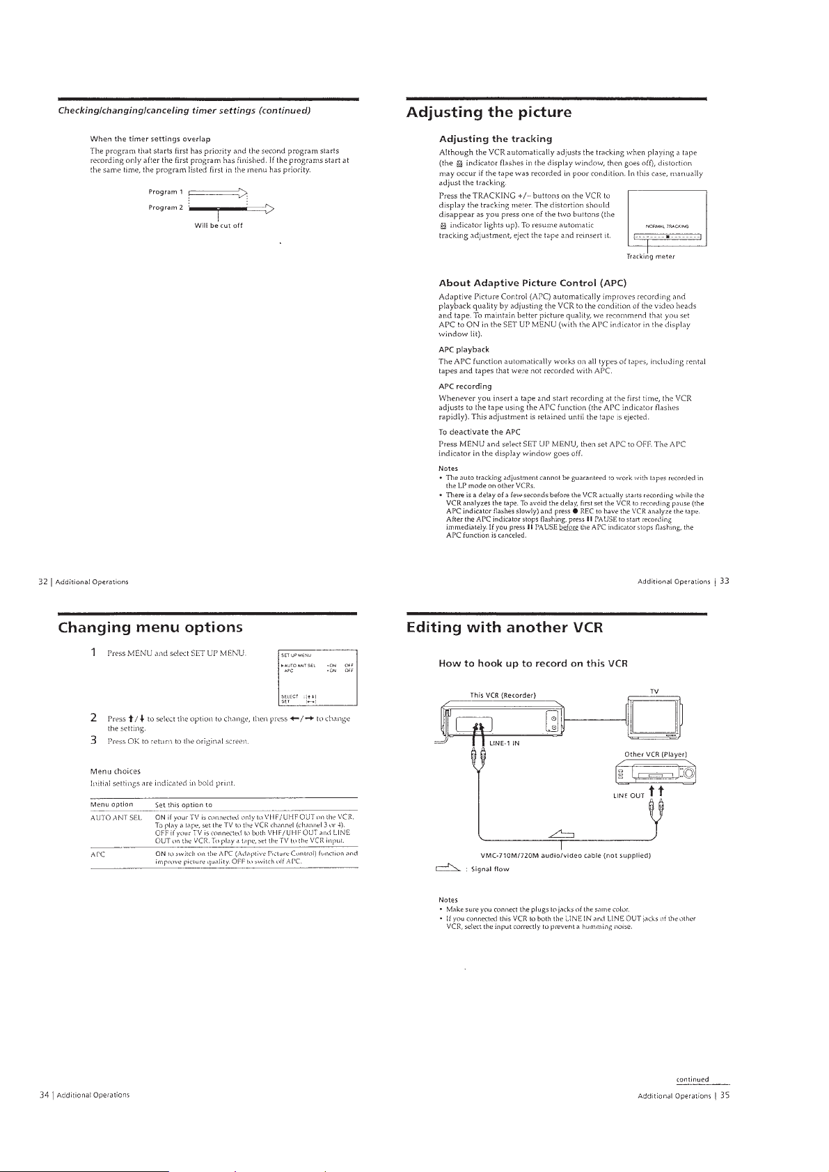
• This set can be disassembled in the order shown below.
Note: Pages in indicated pages in the SERVICE MANUAL.
Pages in indicated pages in the VHS MECHANICAL ADJUSTMENT MANUAL VI.
Set
Upper case
(Page 2-1)
Front Panel
Section
(Page 2-1)
FL Complete
Ass’y
(Page 13)
Retainer
Plate
(Page 22)
FL Slider
Block Ass’y
(Page 22)
Cam Gear
(Page 23)
Pinch Press
Block Ass’y
(Page 14)
Mechanism
Deck
(Page 2-2)
Rubber
Belt
(Page 15)
Capstan
Motor
(Page 15)
Cam Motor
Retainer
(Page 31)
Ground Shaft
Ass’y
(Page 13)
Drum
Ass’y
(Page 13)
Rubber
Belt
(Page 15)
Pully Gear
Ass’y
(Page 29)
Reel Direct
Ass’y
(Page 30)
Rear
Panel
(Page 2-1)
MA-323
Board
(Page 2-2)
Rotary
Switch
(Page 2-2)
Power
Block
(Page 2-2)
Tuner
Unit
NK-11Board
(ED7)
(Page 2-1)
Rubber
Belt
(Page 15)
Slider
(Page 26)
Loading
Gear (T, S)
(Page 28)
Cam Motor
(Page 31)
– 4 –

SECTION 1
GENERAL
SLV-ED1/ED4/ED7/ED8
This section is extracted from SLVED1PL instruction manual.
1-1

1-2
1-3
1-4

1-5

1-6
1-7
1-8
1-9
1-10 E
1-10
SLV-ED1/ED4/ED7/ED8
2 Flat cable
(CN105)
1 Flat cable
(CN424)
ED4/ED7/ED8
4 Three claws
5 Three claws
6 Front panel section
ED7/ED8
3 Connector
(CN423)
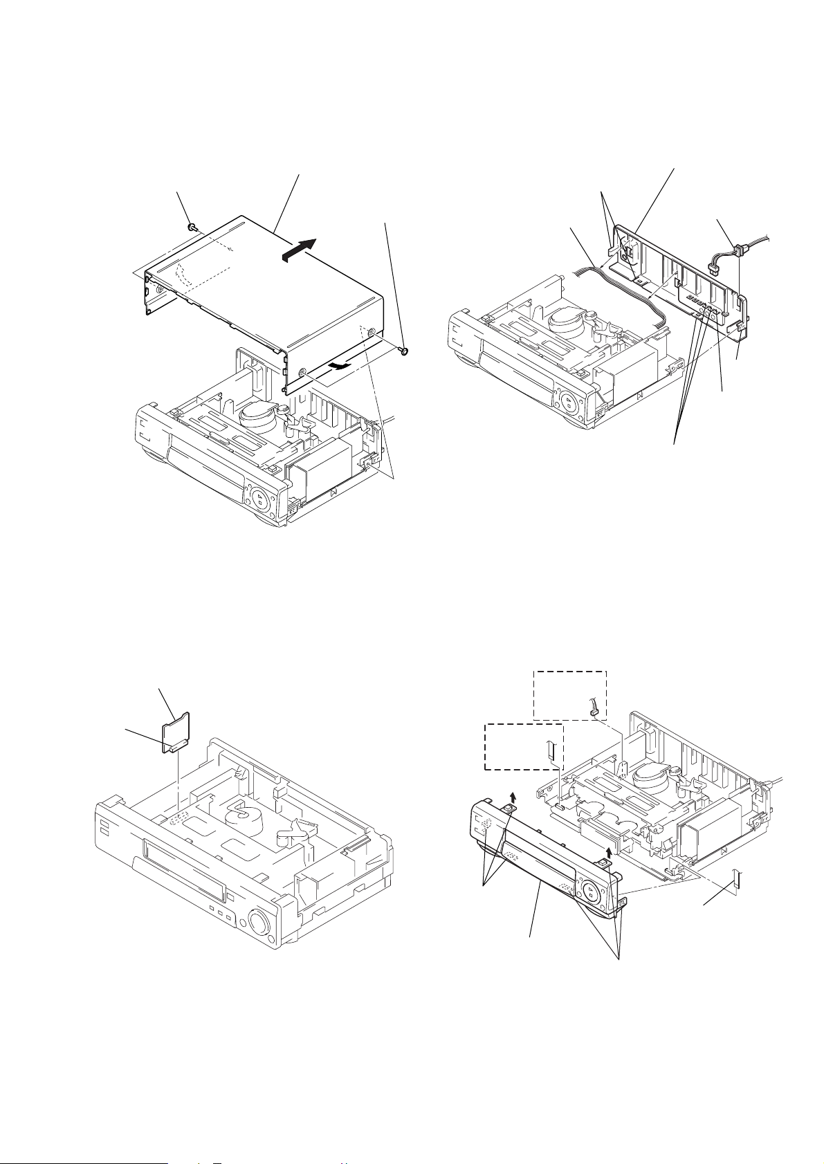
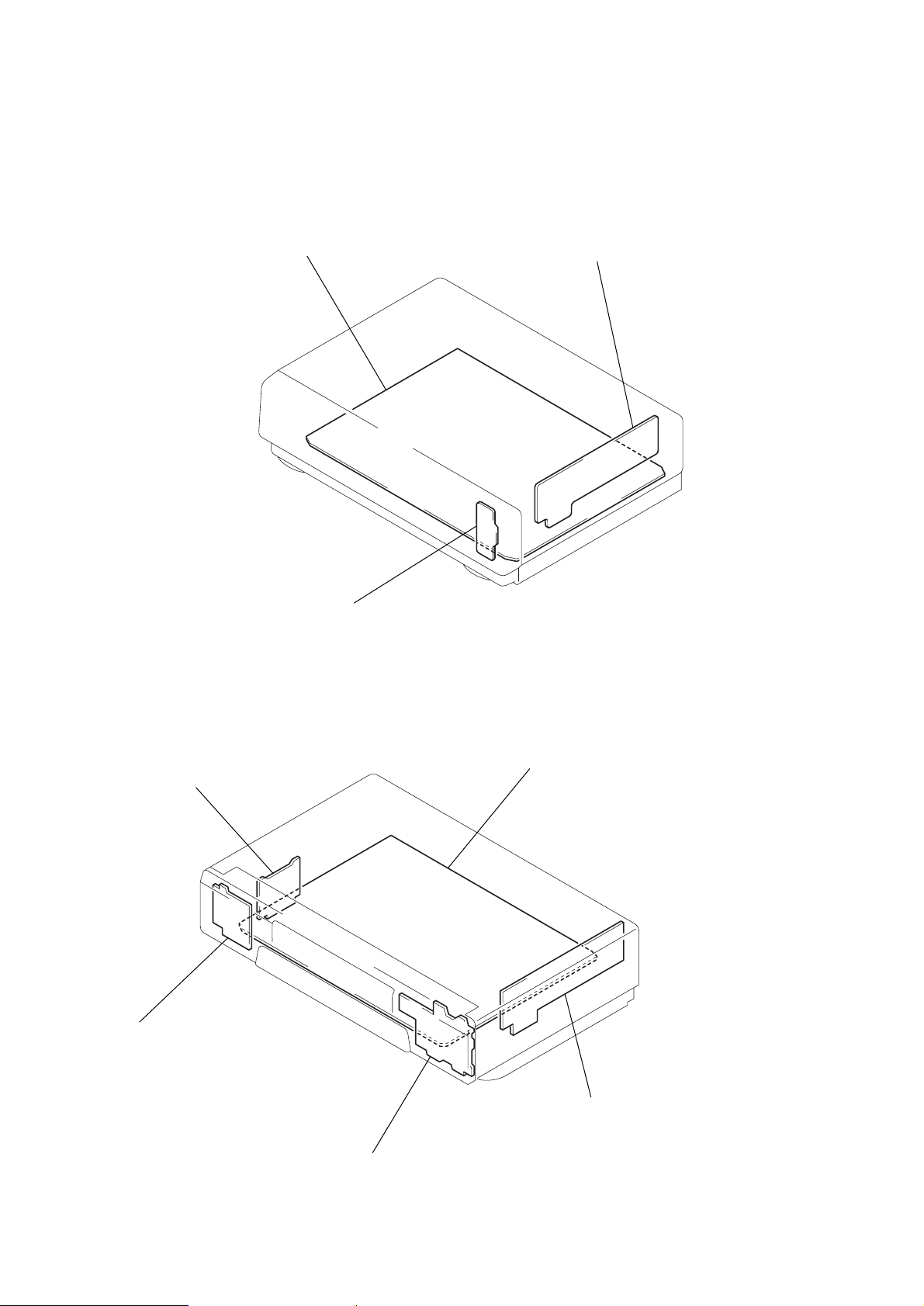
SECTION 2
DISASSEMBLY
Note: Follow the disassembly procedure in the numerical order given.
2-1. UPPER CASE REMOVAL 2-3. REAR PANEL REMOVAL
1 Two tapping screws
3 Upper case
2 Two tapping screws
2 Harness
7 Rear panel
6 Two claws
1 Power cord
4 Claw
3 Claw
(ED4/ED7/ED8)
5 Three claws
2-2. NK-11 BOARD REMOVAL
2 NK-11 board
(ED7)
1 Connector
(CN751)
2-4. FRONT PANEL SECTION REMOVAL
2-1

2-5. POWER BLOCK REMOVAL 2-7. MA-323 BOARD REMOVAL
3 Two screws
4 Power block
(B3)
2 Power cord
(CN101)
1 Connector
(CN600)
ED4/ED7/ED8
1 Five screws
(B3)
2 MA-323
board
2-6. MECHANISM DECK REMOVAL
5 Connector
(FE head )
9 Two screws
(BVTP3 × 12)
2 Connector
(CN101 )
ED4/ED7/
ED8
3 Flexible board
4 Connector
(ACE head )
1 Flat cable
ED1
!¡ Mechanism
!º Screw
8 Screw
(B3)
6 Screw
(B3)
7 Earth lug
deck
(BVTP3 × 12)
3
Note: When mounting the mechanism deck,
first align ¢ mark on the rotary switch.
2-2

2-8. INTERNAL VIEWS
Drum assembly (M901) (DZH-71D-R)
1-759-455-11 (ED1)
Drum assembly (M901) (DZH-73D/Z-RP)
8-839-036-04 (ED4)
Drum assembly (M901) (DZH-94A/ZRP-R)
8-839-044-02 (ED7/ED8)
FE head
1-500-144-11
Q100
Tape top sensor
8-729-043-84
ACE head assembly
A-6759-620-A
D102
Tape top/end LED
8-719-048-26
Q101
Tape end sensor
8-729-043-84
Capstan motor
1-698-971-11
Drum assembly (M901) (DZH-71D-R)
1-759-455-11 (ED1)
Drum assembly (M901) (DZH-73D/Z-RP)
8-839-036-04 (ED4)
Drum assembly (M901) (DZH-94A/ZRP-R)
8-839-044-02 (ED7/ED8)
Cam motor assembly
X-3947-577-1
2-3
2-9. CIRCUIT BOARDS LOCATION
ED1
MA-323
VIDEO, AUDIO, I/O,
(
SERVO/SYSTEM CONTROL, TUNER
)
POWER BLOCK (HS-921SF)
(POWER SUPPLY)
ED4/ED7/ED8
NK-11 (ED7)
(KOREAN STEREO)
MF-312
MODE CONTROL,
(
FRONT IN
DS-80
(MODE CONTROL)
)
MA-323
VIDEO, AUDIO, I/O,
(
SERVO/SYSTEM CONTROL, TUNER
)
DM-76
(MODE CONTROL)
2-4
2-4 E
POWER BLOCK (HS-921SF1)(ED4)
POWER BLOCK (SR-708) (ED7/ED8)
(POWER SUPPLY)
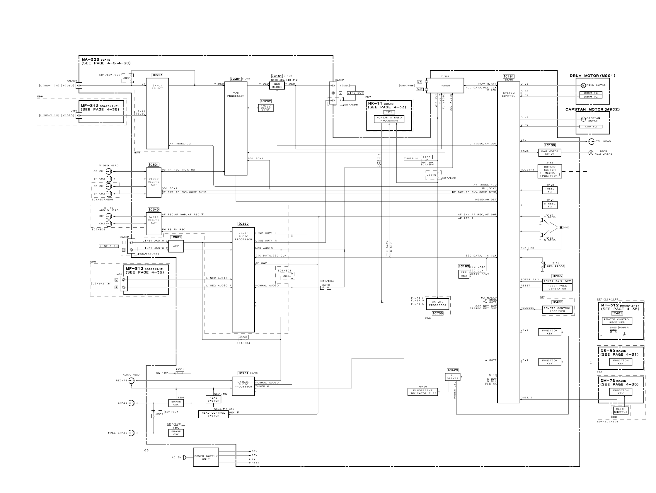
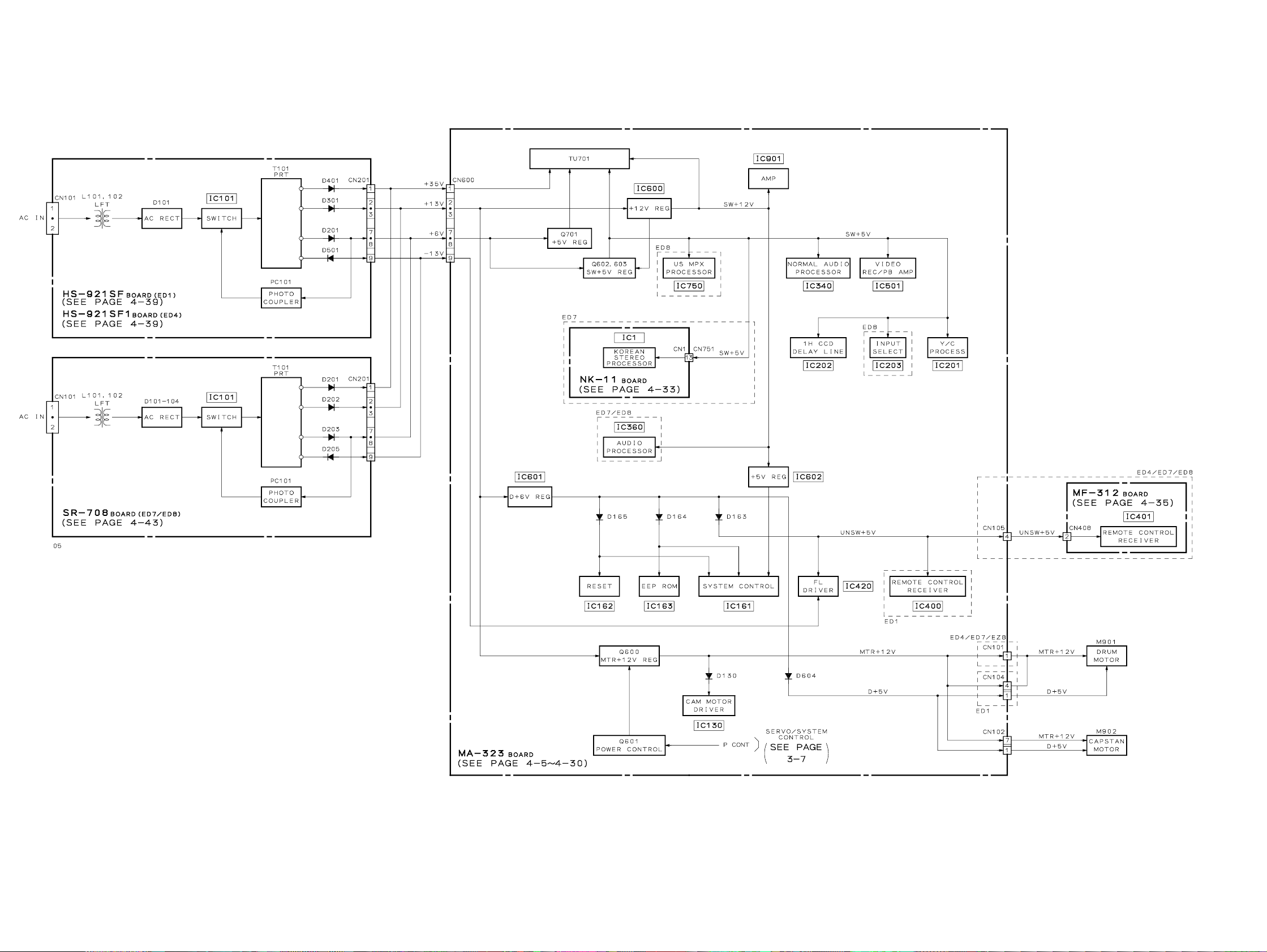
3-1. OVERALL BLOCK DIAGRAM
SLV-ED1/ED4/ED7/ED8
SECTION 3
BLOCK DIAGRAM
3-1 3-2

2.8 Vp-p (H)
2.2 Vp-p (H)
4.6 Vp-p (2 V)
5.2 Vp-p (2 V)
100m Vp-p (H)
800m Vp-p (H)
IC501 4 REC
IC501 !• REC/PB
IC501 @¡ REC
IC501 !¶ REC/PB
IC501 @• REC
IC501 @™ PB
SLV-ED1/ED4/ED7/ED8
3-2. VIDEO1 BLOCK DIAGRAM
3-4

3-3. VIDEO2 BLOCK DIAGRAM
840m Vp-p (H)
400m Vp-p (H)
840m Vp-p (H)
370m Vp-p (H)
1.1 Vp-p (3.58 MHz)
640m Vp-p (H)
5 Vp-p (H)
2.4 Vp-p (14.318 MHz)
2 Vp-p (H)
2.2 Vp-p (H)
1 Vp-p (H)
440m Vp-p (H)
REC: 470m Vp-p (H)
PB: 260m Vp-p (H)
560m Vp-p (H)
REC: 400m Vp-p (H)
PB: 500m Vp-p (H)
REC: 250m Vp-p (H)
PB: 300m Vp-p (H)
360m Vp-p (H)
IC201@§REC/PB
IC2014PB
IC2016REC
IC2017PB
IC201!∞REC
IC201 %º PB
IC201 %£ REC/PB
IC161 $£,$∞ REC/PB
IC161 %™ REC/PB
IC201 %¶ REC/PB
IC201 ^º REC
IC201 &¡ REC/PB
IC201 &¶ REC/PB
IC201 4 REC/PB
IC202 1 REC/PB
IC202 8 REC/PB
IC202 5 REC/PB
SLV-ED1/ED4/ED7/ED8
3-5 3-6

SLV-ED1/ED4/ED7/ED8
4.9 Vp-p (2 V)
3.2 Vp-p (10 MHz)
4.2 Vp-p (360 Hz)
4.7 Vp-p (2 V)
2.2 Vp-p (32.768 kHz)
4 Vp-p (1 kHz)
5 Vp-p (2 V)
5 Vp-p (2 V)
IC161 @¢ REC/PB
IC161 &™ REC/PB
IC161 #• REC/PB
IC161 #ª REC/PB
IC161 ^ª REC/PB
IC161 $º REC/PB
IC161 #¡ REC/PB
IC161 #™ REC/PB
3-4. SERVO/SYSTEM CONTROL BLOCK DIAGRAM
3-7
3-8

3-5. AUDIO BLOCK DIAGRAM
SLV-ED1/ED4/ED7/ED8
3-103-9
SLV-ED1/ED4/ED7/ED8
740m Vp-p (24.576 MHz)
IC1 !§ REC/PB
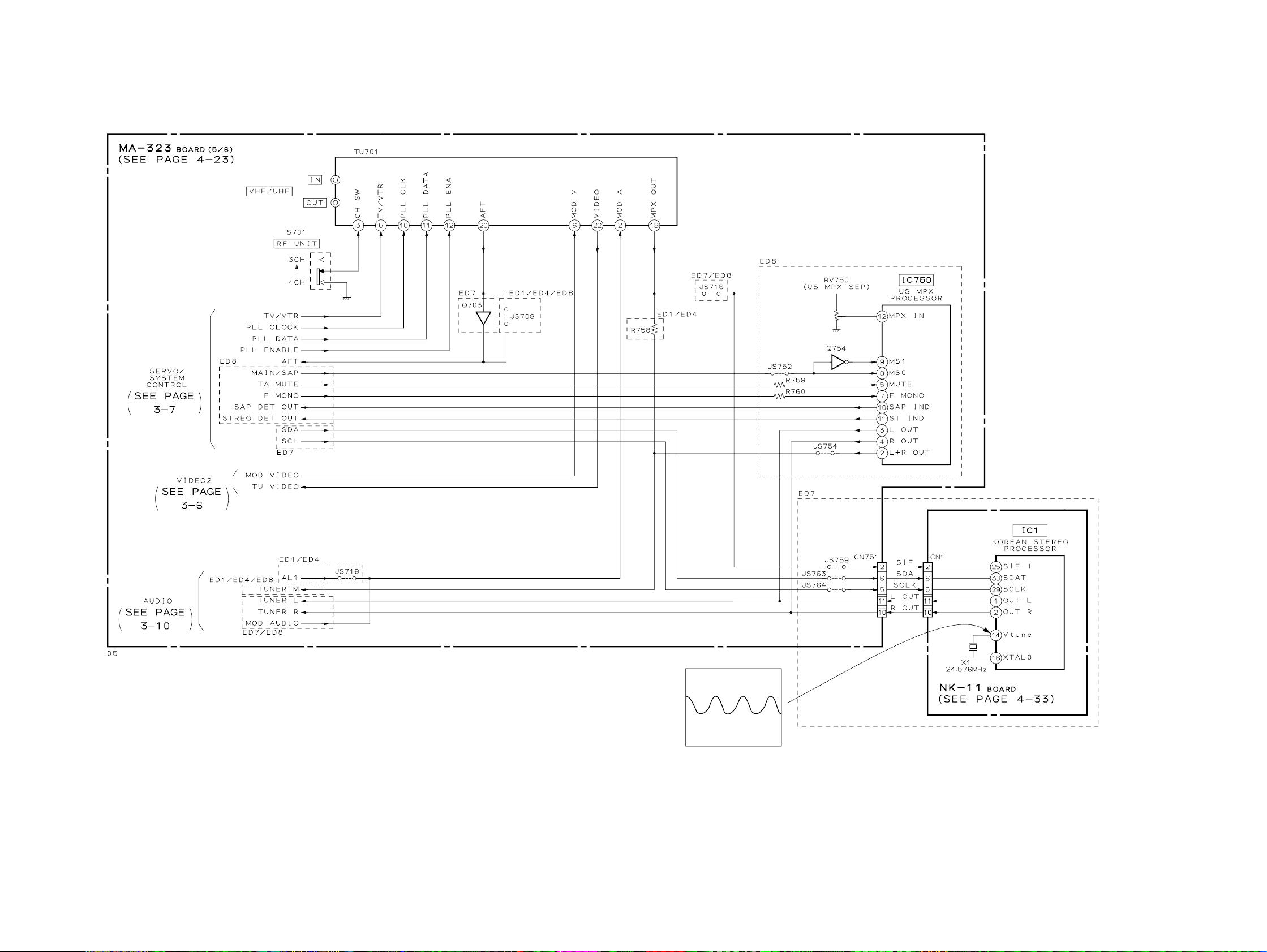
3-6. TUNER BLOCK DIAGRAM
3-11
3-12
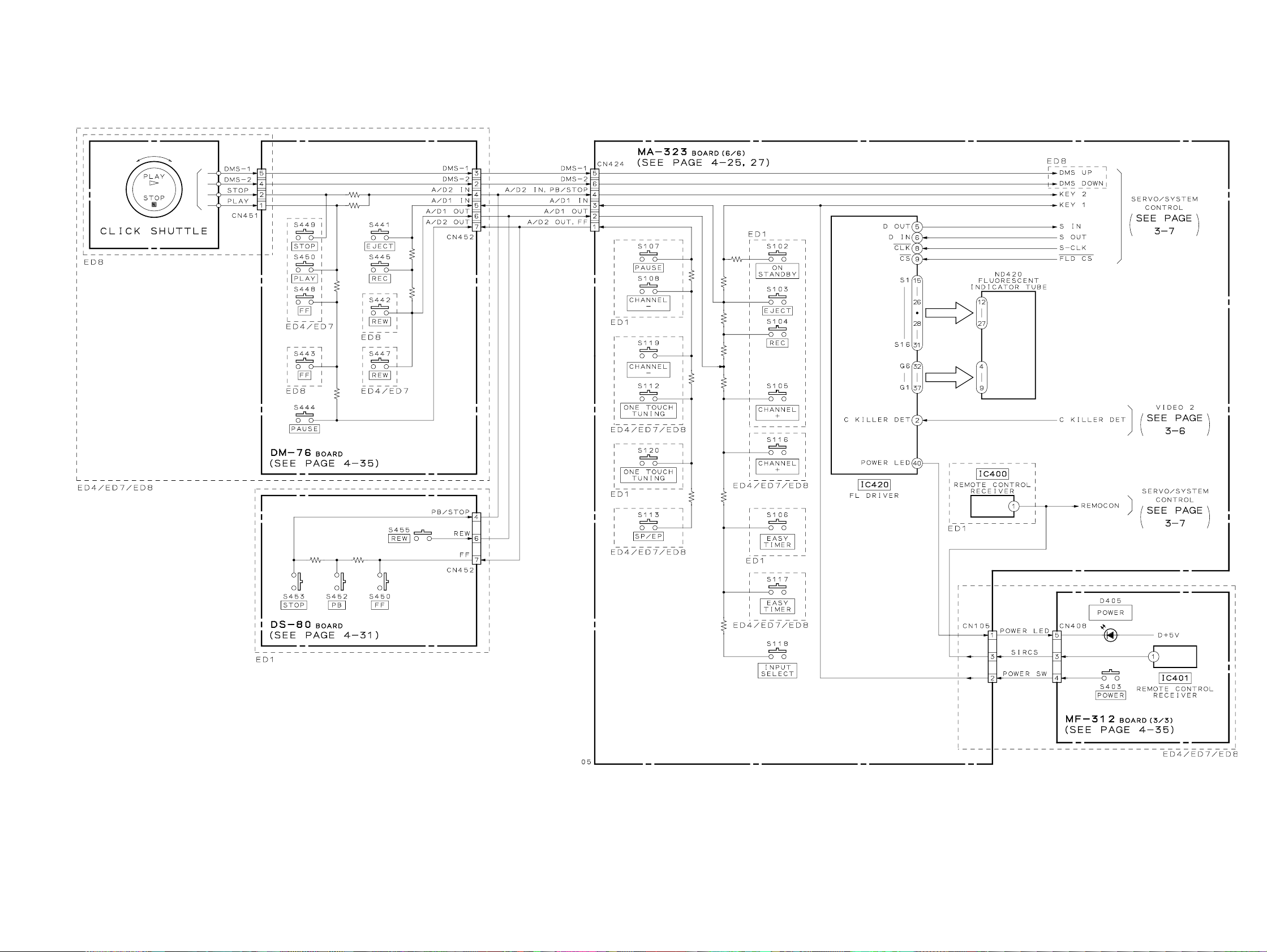
3-7. MODE CONTROL BLOCK DIAGRAM
SLV-ED1/ED4/ED7/ED8
3-143-13
SLV-ED1/ED4/ED7/ED8
3-8. POWER BLOCK DIAGRAM
3-15
3-16 E

SLV-ED1/ED4/ED7/ED8
SECTION 4
PRINTED WIRING BOARDS AND SCHEMATIC DIAGRAMS
THIS NOTE IS COMMON FOR PRINTED WIRING
BOARDS AND SCHEMATIC DIAGRAMS.
(In addition to this, the necessary mote is printed
in each block.)
For printed wiring boards:
• X : indicates a lead wire mounted on the component
side.
• x : indicates a lead wire mounted on the printed side.
• ® : Through hole.
• p : P arts mounted on the conductor side.
• b : Pattern from the side which enables seeing.
Caution:
Pattern face side: Parts on the pattern face side seen from
(Side B) the pattern face are indicated.
Parts face side: Parts on the parts face side seen from
(Side A) the parts face are indicated.
For schematic Diagram:
• Caution when replacing chip parts.
New parts must be attached after removal of chip.
Be careful not to heat the minus side of tantalum capacitor,
because it is damaged by the heat.
• All resistors are in ohms, 1/
less otherwise specified.
kΩ : 1000Ω, MW : 1000kΩ.
• All capacitors are in µF unless otherwise noted. pF : µµF
50V or less are not indicated except for electrolytics and
tantalums.
• All variable and adjustable resistors have characteristic curve
B, unless otherwise noted.
• 2 : nonflammable resistor.
• 5 : fusib le resistor.
• C : panel designation.
• ¢ : internal component.
• C : adjustment for repair.
• U : B+ Line.
• V : B– Line.
• Circled numbers refer to wav eforms.
• Voltages are dc between measurement point.
• Readings are taken with a color-bar signal input.
• Readings are taken with a digital multimeter (DC 10MW).
• Voltage variations may be noted due to normal production
tolerances.
Note:The components identified by mark ! or dotted line
with mark ! are critical for safety.
Replace only with part number specified.
4
W (Chip resistors : 1/
10
W) un-
When indicating parts by reference
number, please include the board
name.
4-1

SLV-ED1/ED4/ED7/ED8
4-1. FRAME SCHEMATIC DIAGRAM
FRAME
4-3 4-4
4-2. PRINTED WIRING BOARD AND SCHEMATIC DIAGRAMS
2.2 Vp-p (H)
RTV servis Horvat
Kešinci, 31402 Semeljci
031-856-139
031-856-637
098-788-319
rtv-servis-horvat@os.tel.hr
Croatia
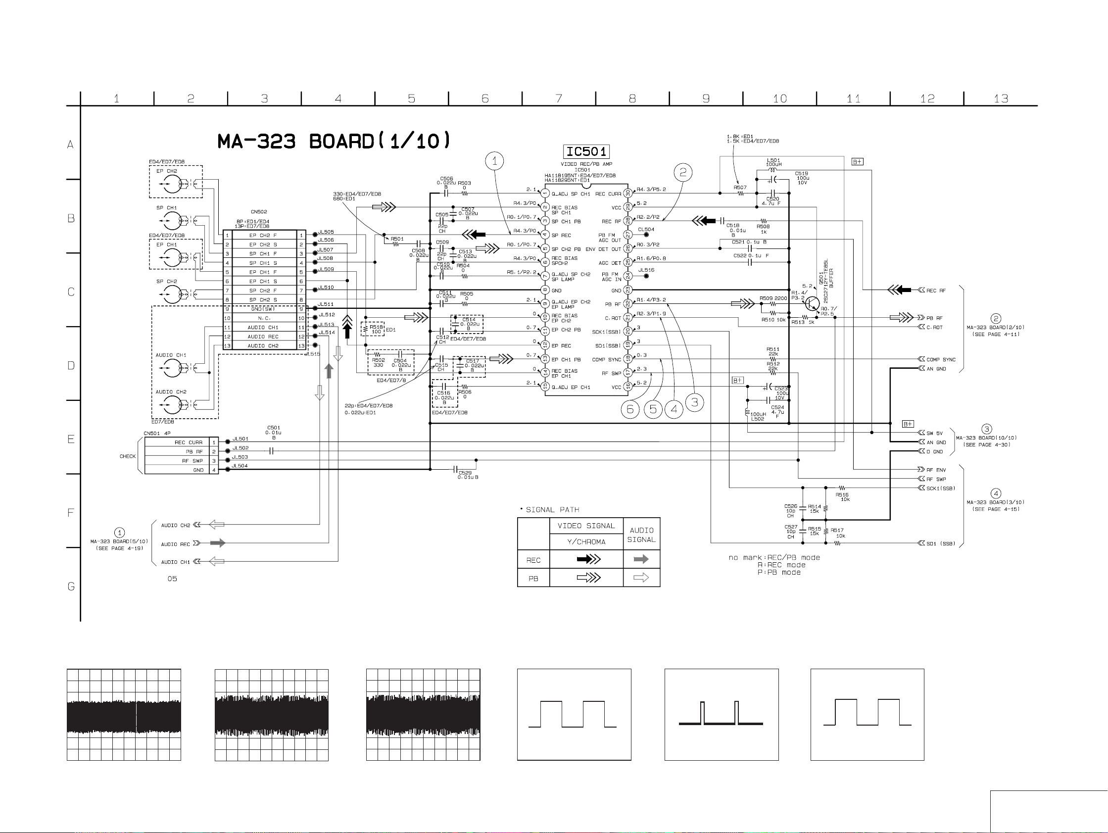
MA-323 (HEAD AMP) SCHEMATIC DIAGRAM • See page 4-9 to 4-10 for printed wiring board.
– Ref. No.: MA-323 board; 2,000 series –
SLV-ED1/ED4/ED7/ED8
• Wavef orms
1 IC501 4 REC
2.8 Vp-p (H)
2 IC501 @• REC 3 IC501 @™ PB 4 IC501 @¡ REC/PB 5 IC501 !• REC/PB 6 IC501 !¶ REC/PB
100m Vp-p (H)
800m Vp-p (H)
4.6 Vp-p (2 V)
5.2 Vp-p (2 V)
4-5 4-6
HEAD AMP
MA-323 (1/10)
SLV-ED1/ED4/ED7/ED8
MA-323
VIDEO, AUDIO, I/O,
(
SERVO/SYSTEM CONTROL, TUNER
DS-80
(MODE CONTROL)
MA-323 BOARD
CN101 F-12
CN102 E-3
CN103 H-6
CN104 H-12
CN105 I-13
CN161 I-12
CN301 B-6
CN302 B-5
CN341 C-12
CN423 D-12
CN424 I-1
CN501 A-9
CN502 B-10
CN600 G-1
CN751 H-13
D102 F-7
D103 F-11
D104 I-5
D105 J-13
D106 G-9
D130 I-4
D163 I-6
D164 I-7
D165 H-6
D305 B-5
D306 D-12
)
POWER BLOCK (HS-921SF)
(POWER SUPPLY)
D307 B-5
D401 J-1
D402 E-8
D403 E-7
D600 H-1
D601 H-1
D602 H-1
D603 I-2
D604 H-5
D701 C-12
D702 C-12
D704 E-12
D908 A-4
D909 A-4
IC130 I-4
IC161 H-8
IC162 I-11
IC163 H-11
IC201 D-5
IC202 E-5
IC203 D-3
IC340 B-11
IC360 D-10
IC400 J-9
IC420 I-7
IC501 B-9
IC600 I-2
IC601 J-2
IC602 D-9
IC750 H-13
IC901 B-2
Q100 F-11
Q101 F-3
Q102 G-6
Q103 H-6
Q105 H-9
Q201 E-4
Q202 D-7
Q204 C-3
Q205 C-3
Q207 D-7
Q208 C-6
Q209 D-7
Q210 D-6
Q301 B-6
Q302 B-6
Q303 B-6
Q305 C-7
Q307 C-6
Q308 C-6
Q311 B-6
Q312 B-6
Q330 B-2
Q331 C-2
Q332 B-6
Q400 E-6
Q402 E-8
Q501 B-9
Q600 G-2
Q601 G-2
Q602 I-1
Q603 I-1
Q701 C-13
Q703 E-13
Q754 H-13
Q901 A-7
NK-11 (ED7)
(KOREAN STEREO)
MF-312
MODE CONTROL,
(
FRONT IN
)
DM-76
(MODE CONTROL)
MA-323
VIDEO, AUDIO, I/O,
(
SERVO/SYSTEM CONTROL, TUNER
POWER BLOCK (HS-921SF1)(ED4)
POWER BLOCK (SR-708) (ED7/ED8)
(POWER SUPPLY)
)
4-8
 Loading...