

Sony SLV-ED10PS, SLV-ED40ME, SLV-ED10SG, SLV-ED10MPS, SLV-ED40PS Service Manual
...
SLV-ED10ME/ED10MPS/ED10PS/ED10SG/ED40ME/ED40PS/ED40SG/ED60ME/
ED60PS/ED60SG/ED70MN/EZ10AZ/EZ40AZ/EZ60AZ/EZ70AS/EZ70NZ
Q
Q
3
7
6
3
1
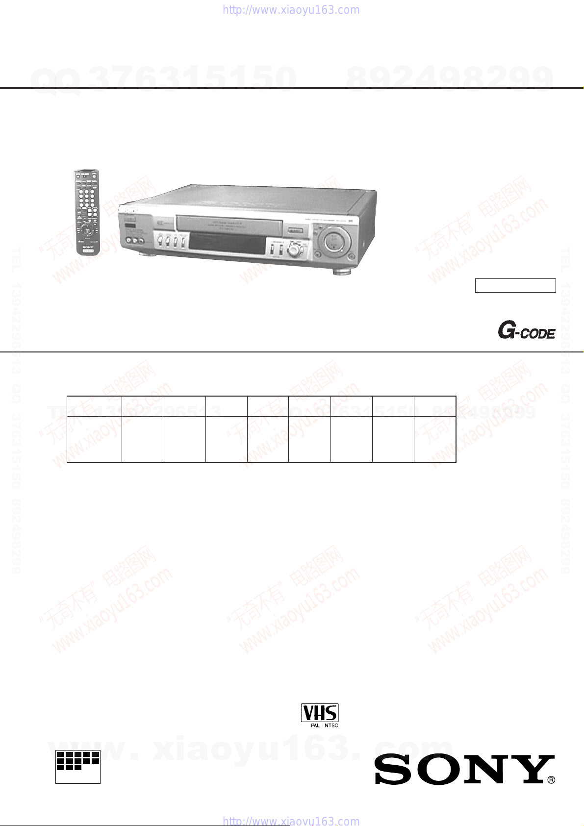
RMT-V245/V245A/V245C/V247/V247C/V247D/V248C
5
1
5
0
SERVICE MANUAL
TEL 13942296513 QQ 376315150 892498299
Photo: SLV-ED70MN
• Refer to the SERVICE MANUAL of VHS MECHANICAL
ADJUSTMENTS VI for MECHANICAL ADJUSTMENTS.
(9-921-647-11)
4
2
9
8
SLV-EZ10AZ/EZ40AZ/EZ60AZ/EZ70AS
SLV-ED10MPS/ED10PS/ED40PS/ED60PS/ED70MN
SLV-EZ10AZ/EZ40AZ/EZ60AZ/EZ70NZ
9
Australian Model
SLV-ED10ME/ED10SG/ED40ME/
ED40SG/ED60ME/ED60SG
Newzealand Model
2
8
9
E Model
ME Model
S MECHANISM
9
G
TEL 13942296513 QQ 376315150 892498299
* The abbreviations of ED10, ED40, ED60, ED70, EZ10, EZ40, EZ60 and EZ70
contained in this service manual are indicated when these models are common to all their corresponding models as given below.
Abbreviated
model name
TEL
13942296513
All model
names
SLV-
ED10
ED10ME
ED10MPS
ED10PS
ED10SG
ED40 ED60
ED40ME
ED40PS
ED40SG
ED60ME
ED60PS
ED60SG
ED70
ED70MN
Q
EZ10
Q
EZ10AZ
3
6
7
EZ40AZ
EZ40
3
EZ60 EZ70
1
5
1
ED60AZ
5
0
EZ70AS
EZ70NZ
8
9
2
4
9
8
2
9
9
w
w
MICROFILM
w
.
xia
o
y
u
1
6
VIDEO CASSETTE RECORDER
3
.
c
o
m
SPECIFICATIONS
7
Q
Q
System
Color system
ED10/ED40/ED60/ED70:
PAL, MESECAM, NTSC 3.58,
NTSC 4.43
EZ10/EZ40/EZ60/EZ70:
PAL, NTSC 4.43
TV system
ED10/ED40/ED60/ED70:
B/G, D/K, I
EZ10/EZ40/EZ60/EZ70:
B/G
Channel coverage
ED10/ED40/ED60/ED70:
B/G: VHF E2 to E12/UHF E21 to E69/
TEL 13942296513 QQ 376315150 892498299
CATV S01 to S05, S1 to S41
D/K: VHF R1 to R12, UHF R21 to R69
I: VHF SA4 to SA13/UHF B21 to B69/
CATV S01 to S05, S1 to S41
EZ10/EZ40/EZ60 (COUNTRY is set to AUS),
EZ70AS:
VHF AS0 to AS12, AS5A, AS9A
UHF AS28 to AS69
CATV S01 to S05, S1 to S41
EZ10/EZ40/EZ60 (COUNTRY is set to NZ),
EZ70NZ:
VHF NZ1 to NZ11
UHF E21 to E69
CATV S01 to S05, S1 to S41
RF output signal
ED10/ED40/ED60/ED70/EZ70NZ:
UHF channels 21 to 69
EZ10/EZ40/EZ60/EZ70AS:
UHF channels 28 to 69
Aerial out
TEL
75-ohm asymmetrical aerial socket
3
13942296513
6
3
1
5
1
5
Inputs and outputs
LINE IN (ED10/EZ10/EZ40/EZ60)
LINE-1 IN (ED40/ED60/ED70/EZ70)
VIDEO IN, phono jack (1)
Input signal: 1 Vp-p, 75 ohms, unbalanced,
sync negative
AUDIO IN (MONO), phono jack (1)
(ED10/ED40/EZ10/EZ40)
AUDIO IN, phono jack (2) (ED60/ED70/
EZ60/EZ70)
Input level: 327 mVrms
Input impedance: more than 47 kilohms
LINE-2 IN (ED40/ED60/ED70/EZ70)
VIDEO IN, phono jack (1)
Input signal: 1Vp-p, 75 ohms, unbalanced,
sync negative
AUDIO IN (MONO), phono jack (2)
(ED40)
AUDIO IN, phono jack (2) (ED60/ED70/
EZ70)
Input level: 327mVrms
Input impedane: more than 47 kilohms
LINE-3 IN (SAT IN) (ED40/ED60/ED70/
EZ70AS)
VIDEO IN, phono jack (1)
Input signal: 1Vp-p, 75 ohms, unbalanced,
sync negative
AUDIO IN (MONO), phono jack (2) (ED40)
AUDIO IN, phono jack (2) (ED60/ED70/
EZ70AS)
Input level: 327mVrms
Input impedane: more than 47 kilohms
LINE OUT (ED10/ED40/EZ10/EZ40)
LINE-1 OUT (ED60/ED70/EZ60/EZ70)
VIDEO OUT, phono jack (1)
Output signal: 1 Vp-p, 75 ohms, unbal-
anced, sync negative
AUDIO OUT, phono jack (1) (ED10/EZ10/
EZ40)
AUDIO OUT (MONO), phono jack (2)
(ED40)
AUDIO OUT, phono jack (2) (ED60/ED70/
EZ60/EZ70)
Standard output: 327 mVrms
Load impedance; 47 kilohms
Output impedance: less than 10 kilohms
0
Q
Q
3
7
4
2
9
8
LINE-2 OUT (AUDIO) (ED60/ED70/EZ60/EZ70)
AUDIO OUT, phono jack (2)
Standard output: 327 mVrms
Load impedance; 47 kilohms
Output impedance: less than 10 kilohms
SKY TV DECODER (EZ70NZ)
VIDEO IN, phono jack (1)
Input signal: 1 Vp-p, 75 ohms, unbalanced,
sync negative
VIDEO OUT, phono jack (1)
Output signal: 1 Vp-p, 75 ohms, unbalanced.
General
Power requirements
110 – 240 V AC, 50/60 Hz (ED10/ED40/
ED60/ED70)
220-240 V AC, 50 Hz (EZ10/EZ40/EZ60/
EZ70)
Power consumption
18W (ED10/ED40/ED60/EZ10/EZ40)
20W (ED70/EZ60/EZ70)
Operating temperature
5 ˚C to 40 ˚C
Storage temperature
–20 ˚C to 60 ˚C
Dimensions
Approx. 355 × 96 × 289 mm (w/h/d):
(ED10/EZ10)
Approx. 430 × 100 × 295 mm (w/h/d):
(ED40/ED60/ED70/EZ40/EZ60/EZ70)
including projecting parts and controls
Mass
Approx. 3.6 kg: (ED10/EZ10)
Approx. 4.2 kg: (ED40)
Approx. 4.5 kg: (ED60/ED70/EZ40/EZ60/
5
1
5
1
3
6
Supplied accessories
Remote commander (1)
R6 (size AA) batteries (2)
Aerial cable (1)
Plug adaptor (1) (ED10ME/ED10SG/ED40ME/
ED40SG/ED60ME/ED60SG)
Design and specifications are subject to change
without notice.
0
8
EZ70)
9
9
8
2
4
2
9
8
9
2
9
9
TEL 13942296513 QQ 376315150 892498299
9
SAFETY CHECK-OUT
After correcting the original service problem, perform the following
safety checks before releasing the set to the customer:
1. Check the area of your repair for unsoldered or poorly-soldered connections. Check the entire board surface for solder
splashes and bridges.
2. Check the interboard wiring to ensure that no wires are
“pinched” or contact high-wattage resistors.
3. Look for unauthorized replacement parts, particularly transistors, that were installed during a previous repair. Point them
out to the customer and recommend their replacement.
SAFETY-RELATED COMPONENT WARNING!!
COMPONENTS IDENTIFIED BY MARK ! OR DOTTED
LINE WITH MARK ! ON THE SCHEMATIC DIAGRAMS
AND IN THE PARTS LIST ARE CRITICAL TO SAFE
w
w
w
.
OPERATION. REPLACE THESE COMPONENTS WITH
xia
SONY PARTS WHOSE PART NUMBERS APPEAR AS
SHOWN IN THIS MANUAL OR IN SUPPLEMENTS PUBLISHED BY SONY.
o
y
4. Look for parts which, though functioning, show obvious signs
of deterioration. Point them out to the customer and recommend their replacement.
5. Check the B+ voltage to see it is at the values specified.
u
1
6
3
.
c
o
m
– 2 –
• Feature Difference
7
Q
Q
TEL 13942296513 QQ 376315150 892498299
3
FEATURE AS NZ
HEAD/CH 2/2 4/4 4/6 4/6 2/2 4/4 4/6 4/6 4/6
NTSC (3.58) (REC/PB) ggggGGGgg
ME-SECAM (REC/PB) ggggGGGGG
REC (NTSC) (SP/EP) ggggGGGgg
(PAL) (SP/LP) ggggggggg
PLAY (NTSC) (SP/LP/EP) ggggggggg
(PAL) (SP/LP) ggggggggg
RCA REAR LINE INPUT gg
RCA REAR LINE OUTPUT g
ADDITIONAL REAR INPUT (SAT IN) G
ADDITIONAL REAR OUTPUT
(AUDIO OUT)
SKYDECODER REAR IN/OUT GGGGGGGGg
RCA FRONT LINE INPUT G
MODULATOR SYSTEM G/K/I G/K/I G/K/I G/K/I G G G G G
CLICK SHUTTLE GGGgGGGgg
REMOTE COMMANDER RMT- V248C V247 V247C V247D V245A V245A V245C V245 V245
6
1
5
1
3
(4.43) (REC/PB) ggggG/gG/gG/gg g
SLV- ED10 ED40 ED60 ED70 EZ10 EZ40 EZ60 EZ70 EZ70
5
0
g (3pin g (3pin
Y.W.R) Y.W.R) Y.W.R) Y.W.R) Y.W.R)
g (3pin g (3pin g (3pin
Y.B.B) Y.W.R) Y.W.R) Y.W.R) Y.W.R) Y.W.R)
g (3pin g (3pin g (3pin
Y.B.B) Y.W.R) Y.W.R) Y.W.R)
GGggGGggg
g (3pin g (3pin g (3pin
Y.B.B) Y.W.R) Y.W.R) Y.W.R) Y.W.R)
8
4
2
9
gg
gg
GGG
GGG
9
g (3pin g (3pin g (3pin
g (3pin g (3pin g (3pin
2
8
g (3pin
g (3pin g (3pin
9
G
9
TEL 13942296513 QQ 376315150 892498299
TEL
13942296513
Q
Q
3
7
6
3
1
5
1
5
0
8
9
2
4
9
8
2
9
9
w
w
w
.
xia
o
y
u
1
6
– 3 –
3
.
c
o
m
TABLE OF CONTENTS
7
Q
Q
Section Title Page Section Title Page
Feature Difference................................................................... 3
SERVICE NOTE ...................................................................... 5
1. GENERAL
Getting Started .............................................................. 1-1
Basic Operations ........................................................... 1-4
Additional Operations.................................................... 1-8
Editing............................................................................ 1-11
Additional Information ................................................... 1-12
2. DISASSEMBLY
TEL 13942296513 QQ 376315150 892498299
2-1. Upper Case Removal .................................................... 2-1
2-2. GK-12, NK-11, RJ-82 Board Removal .......................... 2-1
2-3. Rear Panel Removal ..................................................... 2-1
2-4. Front Panel Section Removal ....................................... 2-1
2-5. Power Block Removal ................................................... 2-2
2-6. Mechanism Deck Removal ........................................... 2-2
2-7. MA-350 board Removal ................................................ 2-2
2-8. Internal Views ................................................................ 2-3
2-9. Circuit Boards Location ................................................. 2-4
3. BLOCK DIAGRAMS
3-1. Overall Block Diagram .................................................. 3-1
3-2. Servo/System Control Block Diagram .......................... 3-3
3-3. Video Block Diagram..................................................... 3-5
3-4. Audio Block Diagram..................................................... 3-7
TEL
3-5. Tuner Block Diagram ..................................................... 3-9
3-6. Mode Control Block Diagram ........................................ 3-11
3-7. Power Block Diagram.................................................... 3-13
4. PRINTED WIRING BOARDS AND
SCHEMATIC DIAGRAMS
4-1. Frame Schematic Diagram ........................................... 4-3
4-2. Printed Wiring Boards and Schematic Diagrams ......... 4-5
MA-350 Printed Wiring Board ....................................... 4-5
MA-350 (Video, Audio) Schematic Diagram ................. 4-9
MA-350 (System Control) Schematic Diagram ............ 4-13
MA-350 (Servo Control) Schematic Diagram ............... 4-15
MA-350 (Hi-Fi Audio) Schematic Diagram.................... 4-17
MA-350 (I/O) Schematic Diagram................................. 4-19
MA-350 (Tuner) Schematic Diagram ............................ 4-21
MA-350 (FL Drive) Schematic Diagram........................ 4-23
MA-350 (Mode Control) Schematic Diagram ............... 4-25
MA-350 (Power Supply) Schematic Diagram............... 4-27
NK-11 Printed Wiring Board and
Schematic Diagram....................................................... 4-29
GK-12 Printed Wiring Board and
Schematic Diagram....................................................... 4-31
DM-85 Printed Wiring Board and
Schematic Diagrams ..................................................... 4-33
MF-317 Printed Wiring Board and
Schematic Diagram....................................................... 4-35
KK-19 Printed Wiring Board and
Schematic Diagram....................................................... 4-37
DS-85, KK-18 Printed Wiring Boards and
Schematic Diagrams ..................................................... 4-39
RJ-82 Printed Wiring Board and
Schematic Diagram ....................................................... 4-41
HS-921SF/921SF1 Printed Wiring Board ..................... 4-43
HS-921SF/921SF1 Schematic Diagram ....................... 4-45
w
SR-708/718 Printed Wiring Board ................................ 4-47
SR-708/718 Schematic Diagram .................................. 4-49
3
13942296513
w
w
6
.
1
3
xia
5
o
1
y
5
u
0
5. INTERFACE, IC PIN FUNCTION DESCRIPTION
5-1. System Control-Video Block Interface
(MA-350 BOARD IC161)............................................... 5-1
5-2. System Control-Servo Peripheral Circuit Interface
(MA-350 BOARD IC161)............................................... 5-1
5-3. System Control-Mechanism Block Interface
(MA-350 BOARD IC161)............................................... 5-2
5-4. System Control-Audio Block Interface
(MA-350 BOARD IC161)............................................... 5-3
5-5. Servo/System/Tuner/Timer/MODE Control,
OSD Microprocessor Pin Function
(MA-350 BOARD IC161)............................................... 5-4
5-6. NICAM Processor Pin Function
(NK-11 BOARD IC1)...................................................... 5-5
5-7. ZWEITON Processor Pin Function
(GK-12 BOARD IC001) ................................................. 5-5
6. ERROR CODES ....................................................... 6-1
7. ADJUSTMENTS
7-1. Mechanical Adjustments ............................................... 7-1
7-2. Electrical Adjustments ................................................... 7-1
2-1. Pre-Adjustment Preparations........................................ 7-1
2-1-1. Instruments to be Used............................................ 7-1
2-1-2. Connection ............................................................... 7-1
2-1-3. Set-up of Adjustment................................................ 7-1
2-1-4. Alignment Tapes....................................................... 7-1
2-1-5. Specified I/O Level and Impedance......................... 7-1
3
Q
Q
2-1-6. Adjusting Sequence ................................................. 7-2
2-2. Power Supply Adjustments ........................................... 7-2
2-2-1. Power Supply Check................................................ 7-2
2-2-2. +6 V Adjustment ....................................................... 7-2
2-3. Servo System Adjustment ............................................. 7-2
2-3-1. RF Switching Position Adjustment........................... 7-2
2-4. Audio System Adjustments ........................................... 7-3
2-4-1. Hi-Fi Audio System Adjustment ............................... 7-3
1. AF Switching Position Adjustment ........................... 7-3
2. Frequency Response Check.................................... 7-3
3. Overall Level Characteristic and
4. Overall S/N Check.................................................... 7-4
2-4-2. Normal Audio System Adjustment ........................... 7-4
1. ACE Head Adjustment ............................................. 7-4
2. E-E Output Level Check .......................................... 7-4
3. Frequency Responce Check.................................... 7-4
4. Overall Level Characteristic and Distortion
5. Overall S/N Check.................................................... 7-5
2-5. Tuner System Adjustment ............................................. 7-5
2-5-1. Separation Adjustment............................................. 7-5
2-6. Parts Arrangement Diagram for Adjustments ............... 7-6
8. REPAIR PARTS LIST
8-1. Exploded Views ............................................................. 8-1
8-1-1. Front Panel and Cabinet Assemblies
8-1-2. Chassis Assembly (ED10/EZ10).............................. 8-2
8-1-3. Front Panel and Cabinet Assemblies
8-1-4. Chassis Assembly
8-1-5. Mechanism Chassis Assembly (1)........................... 8-6
8-1-6. Mechanism Chassis Assembly (2)........................... 8-7
1
6
8-1-7. Mechanism Chassis Assembly (3)........................... 8-8
8-2. Electrical Parts List........................................................ 8-9
8
3
6
7
Distortion Factor Check ........................................... 7-4
Factor Check ............................................................ 7-5
(ED10/EZ 10 ) ............................................................ 8-1
(ED40/ED60/ED70/EZ40/EZ60/EZ70) .................... 8-3
(ED40/ED60/ED70/EZ40/EZ60/EZ70) .................... 8-5
3
.
9
1
1
5
c
2
5
o
0
m
9
8
9
8
2
4
4
2
9
8
9
2
9
9
TEL 13942296513 QQ 376315150 892498299
9
– 4 –
Q
7
Q
3
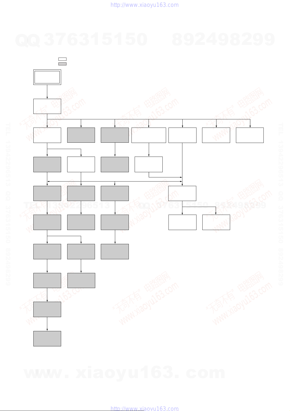
1. DISASSEMBLY
• This set can be disassembled in the order shown below.
Note: Pages in indicated pages in the SERVICE MANUAL.
Pages in indicated pages in the VHS MECHANICAL ADJUSTMENT MANUAL VI.
Set
Upper case
(Page 2-1)
6
3
1
5
1
SERVICE NOTE
5
0
8
9
2
4
9
8
2
9
9
TEL 13942296513 QQ 376315150 892498299
FL Complete
TEL
Block Ass’y
Front Panel
Section
(Page 2-1)
Ass’y
(Page 13)
Retainer
Plate
(Page 22)
13942296513
FL Slider
(Page 22)
Cam Gear
(Page 23)
Pinch Press
Block Ass’y
(Page 14)
Mechanism
Deck
(Page 2-2)
Rubber
Belt
(Page 15)
Capstan
Motor
(Page 15)
Cam Motor
Retainer
(Page 31)
Ground Shaft
Ass’y
(Page 13)
Drum
Ass’y
(Page 13)
Rubber
Belt
(Page 15)
Pully Gear
Ass’y
(Page 29)
Reel Direct
Ass’y
(Page 30)
RJ-82 Board (EXCEPT
ED10/EZ10/EZ40
(Page 2-1)
Rear
Panel
(Page 2-1)
Q
Q
3
)
7
Power
Block
(Page 2-2)
MA-323
Board
(Page 2-2)
3
6
Rotary
Switch
(Page 2-2)
1
5
1
5
GK-12 Board
(EZ70: AS)
(Page 2-1)
8
0
Tuner
Unit
9
(ED70/EZ70: NZ
9
4
2
NK-11 Board
(Page 2-1)
9
2
8
TEL 13942296513 QQ 376315150 892498299
)
9
w
w
Rubber
Belt
(Page 15)
Slider
(Page 26)
Loading
Gear (T, S)
(Page 28)
w
Cam Motor
(Page 31)
.
xia
o
y
u
1
6
– 5 –
3
.
c
o
m
SLV-ED10/ED40/ED60/ED70/EZ10/EZ40/EZ60/EZ70
SECTION 1
GENERAL
7
Q
Q
TEL 13942296513 QQ 376315150 892498299
3
6
3
1
5
1
5
0
8
This section is extracted from SLV -ED70MN
instruction manual. (3-865-382-11)
9
2
4
9
8
2
9
9
TEL 13942296513 QQ 376315150 892498299
TEL
13942296513
Q
Q
3
7
6
3
1
5
1
5
0
8
9
2
4
9
8
2
9
9
w
w
w
.
xia
o
y
u
1
6
1-1
3
.
c
o
m
7
Q
Q
TEL 13942296513 QQ 376315150 892498299
3
6
3
1
5
1
5
0
8
9
2
4
9
8
2
9
9
TEL 13942296513 QQ 376315150 892498299
TEL
13942296513
Q
Q
3
7
6
3
1
5
1
5
0
8
9
2
4
9
8
2
9
9
w
w
w
.
xia
o
y
u
1
6
1-2
3
.
c
o
m
7
Q
Q
TEL 13942296513 QQ 376315150 892498299
3
6
3
1
5
1
5
0
8
9
2
4
9
8
2
9
9
TEL 13942296513 QQ 376315150 892498299
TEL
13942296513
Q
Q
3
7
6
3
1
5
1
5
0
8
9
2
4
9
8
2
9
9
w
w
w
.
xia
o
y
u
1
6
1-3
3
.
c
o
m
7
Q
Q
TEL 13942296513 QQ 376315150 892498299
3
6
3
1
5
1
5
0
8
9
2
4
9
8
2
9
9
TEL 13942296513 QQ 376315150 892498299
TEL
13942296513
Q
Q
3
7
6
3
1
5
1
5
0
8
9
2
4
9
8
2
9
9
w
w
w
.
xia
o
y
u
1
6
1-4
3
.
c
o
m
7
Q
Q
TEL 13942296513 QQ 376315150 892498299
3
6
3
1
5
1
5
0
8
9
2
4
9
8
2
9
9
TEL 13942296513 QQ 376315150 892498299
TEL
13942296513
Q
Q
3
7
6
3
1
5
1
5
0
8
9
2
4
9
8
2
9
9
w
w
w
.
xia
o
y
u
1
6
1-5
3
.
c
o
m
7
Q
Q
TEL 13942296513 QQ 376315150 892498299
3
6
3
1
5
1
5
0
8
9
2
4
9
8
2
9
9
TEL 13942296513 QQ 376315150 892498299
TEL
13942296513
Q
Q
3
7
6
3
1
5
1
5
0
8
9
2
4
9
8
2
9
9
w
w
w
.
xia
o
y
u
1
6
1-6
3
.
c
o
m
7
Q
Q
TEL 13942296513 QQ 376315150 892498299
3
6
3
1
5
1
5
0
8
9
2
4
9
8
2
9
9
TEL 13942296513 QQ 376315150 892498299
TEL
13942296513
Q
Q
3
7
6
3
1
5
1
5
0
8
9
2
4
9
8
2
9
9
w
w
w
.
xia
o
y
u
1
6
1-7
3
.
c
o
m
7
Q
Q
TEL 13942296513 QQ 376315150 892498299
3
6
3
1
5
1
5
0
8
9
2
4
9
8
2
9
9
TEL 13942296513 QQ 376315150 892498299
TEL
13942296513
Q
Q
3
7
6
3
1
5
1
5
0
8
9
2
4
9
8
2
9
9
w
w
w
.
xia
o
y
u
1
6
1-8
3
.
c
o
m
7
Q
Q
TEL 13942296513 QQ 376315150 892498299
3
6
3
1
5
1
5
0
8
9
2
4
9
8
2
9
9
TEL 13942296513 QQ 376315150 892498299
TEL
13942296513
Q
Q
3
7
6
3
1
5
1
5
0
8
9
2
4
9
8
2
9
9
w
w
w
.
xia
o
y
u
1
6
1-9
3
.
c
o
m
7
Q
Q
TEL 13942296513 QQ 376315150 892498299
3
6
3
1
5
1
5
0
8
9
2
4
9
8
2
9
9
TEL 13942296513 QQ 376315150 892498299
TEL
13942296513
Q
Q
3
7
6
3
1
5
1
5
0
8
9
2
4
9
8
2
9
9
w
w
w
.
xia
o
y
u
1
6
1-10
3
.
c
o
m
7
Q
Q
TEL 13942296513 QQ 376315150 892498299
3
6
3
1
5
1
5
0
8
9
2
4
9
8
2
9
9
TEL 13942296513 QQ 376315150 892498299
TEL
13942296513
Q
Q
3
7
6
3
1
5
1
5
0
8
9
2
4
9
8
2
9
9
w
w
w
.
xia
o
y
u
1
6
1-11
3
.
c
o
m
7
Q
Q
TEL 13942296513 QQ 376315150 892498299
3
6
3
1
5
1
5
0
8
9
2
4
9
8
2
9
9
TEL 13942296513 QQ 376315150 892498299
TEL
13942296513
Q
Q
3
7
6
3
1
5
1
5
0
8
9
2
4
9
8
2
9
9
w
w
w
.
xia
o
y
u
1
6
1-12 E
1-12
3
.
c
o
m
Q
SLV-ED10/ED40/ED60/ED70/EZ10/EZ40/EZ60/EZ70
SECTION 2
DISASSEMBLY
Note: Follow the disassembly procedure in the numerical order given.
7
Q
3
2-1. UPPER CASE REMOVAL 2-3. REAR PANEL REMOVAL
6
3
1
5
1
5
0
8
9
2
4
9
8
2
9
9
3 Upper case
1 Two tapping screws
2 Two tapping screws
TEL 13942296513 QQ 376315150 892498299
2 Harness
7 Rear panel
6 Two claws
1 Power cord
(CN101)
TEL 13942296513 QQ 376315150 892498299
3 Claw
4 Claw
(EXCEPT
ED10/EZ10)
5 Three claws
TEL
13942296513
2-2. GK-12, NK-11, RJ-82 BOARD REMOVAL
7 RJ-82 board
(EXCEPT ED10/
EZ10/EZ40)
2 NK-11 board
(ED70/EZ70NZ)
GK-12 board
(EZ70AS)
1 Connector
(CN751:
ED70/EZ70)
3 Connector
(CN954: EZ70NZ)
4 Connector
(CN951: ED60/ED70/EZ70AS,
CN952: ED40,
CN953: EZ60/EZ70NZ)
5 Two screws
(BVTP3 × 12)
(ED60/ED70/
EZ60/EZ70)
6 Two screws
(BVTP3 × 12)
(ED40/ED60/
ED70/EZ70)
Q
Q
9
2
8
9
4
2
9
8
0
5
1
5
1
3
6
7
3
2-4. FRONT PANEL SECTION REMOVAL
5 Connector
(CN481: ED40/
ED60/ED70/EZ70)
7 Three claws
8 Front panel section
3 Flat cable
(CN451: ED40/ED70/EZ70,
CN454: ED60/EZ40/EZ60)
4 Connector
(CN423)
2 Connector
(CN450)
6 Three claws
1 Flat cable
(CN452: EXCEPT ED10/EZ10,
CN453: ED10/EZ10)
9
w
w
w
.
xia
o
y
u
1
6
2-1
3
.
c
o
m
2-5. POWER BLOCK REMOVAL 2-7. MA-350 BOARD REMOVAL
Q
Q
3 MA-350
board
7
3
2 Three screws
(B3)
6
3
1
5
1 Screw (B3)
(EXCEPT
ED10/EZ10)
1
5
0
9
8
4 Power block
4
2
3 Two screws
(B3)
9
2
8
2 Power cord
9
9
TEL 13942296513 QQ 376315150 892498299
2-6. MECHASISM DECK REMOVAL
TEL
7 Two screws
(BVTP3 × 12)
3 Connector
(CN101: EXCEPT
ED10/EZ10)
13942296513
5 Connector
4 Connector
(FE head )
(ACE head )
1 Flat cable
(ED10/EZ10)
9 Mechanism
deck
8 Screw
(BVTP3 × 12)
Q
Q
3
7
6
3
1
5
1
5
0
1 Connector
(CN600)
(EXCEPT
ED10/EZ10)
2
9
8
4
9
8
2
9
TEL 13942296513 QQ 376315150 892498299
9
2 Flexible board
(CN201: ED10/EZ10,
CN260: EXCEPT
ED10/EZ10)
w
w
3
6 Screw
(B3)
w
.
xia
Note: When mounting the mechanism deck,
first align ¢ mark on the rotary switch.
o
y
u
1
6
3
.
2-2
c
o
m
2-8. INTERNAL VIEWS
7
Q
Q
TEL 13942296513 QQ 376315150 892498299
3
6
FE head
1-500-144-11
Q100
Tape top sensor
8-729-043-84
3
1
5
1
5
0
Drum assembly (M901) (DZH-89A-R)
1-759-453-11 (ED10/EZ10)
Drum assembly (M901) (DZH-74E/Z-RP)
8-839-037-04 (ED40/EZ40)
Drum assembly (M901) (DZH-95A/Z-RP)
8-839-045-02 (ED60/ED70/EZ60/EZ70)
2
9
8
ACE head assembly
A-6759-620-A
4
2
8
9
D102
Tape top/end LED
8-719-048-26
9
9
TEL 13942296513 QQ 376315150 892498299
TEL
13942296513
Capstan motor
1-698-971-11
8
0
5
1
5
1
3
6
7
3
Q
Q
Drum assembly (M901) (DZH-89A-R)
1-759-453-11 (ED10/EZ10)
Drum assembly (M901) (DZH-74E/Z-RP)
8-839-037-04 (ED40/EZ40)
Drum assembly (M901) (DZH-95A/Z-RP)
8-839-045-02 (ED60/ED70/EZ60/EZ70)
Q101
Tape end sensor
8-729-043-84
9
4
2
9
8
2
9
9
w
w
w
.
xia
o
y
u
1
6
Cam motor assembly
X-3947-577-1
2-3
3
.
c
o
m
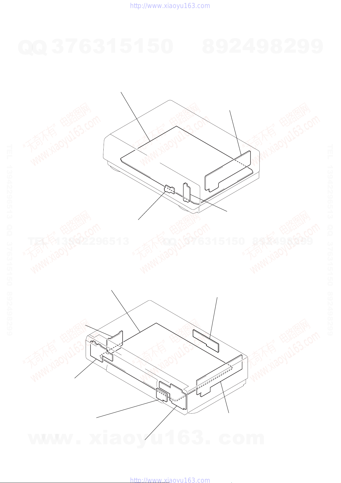
2-9. CIRCUIT BOARDS LOCATION
Q
Q
ED10/EZ10
3
MA-350
VIDEO, AUDIO, I/O,
(
SERVO/SYSTEM CONTROL, TUNER
7
6
3
1
5
1
5
0
)
8
POWER BLOCK
(
(POWER SUPPLY)
4
2
9
HS-921SF: ED10
SR-718: EZ10
9
)
8
2
9
9
TEL 13942296513 QQ 376315150 892498299
KK-18
(EASY TIMER)
TEL
EXCEPT ED10/EZ10
NK-11 (ED70/EZ70: NZ)
(NICAM)
GK-12 (EZ70: AS)
(ZVEI TONE)
13942296513
MA-350
VIDEO, AUDIO, I/O,
(
SERVO/SYSTEM CONTROL, TUNER
Q
Q
)
7
3
RJ-82 (EXCEPT EZ40)
(ADDITIONAL REAR IN/OUT)
6
3
1
DS-85
(MODE CONTROL)
9
8
0
5
1
5
2
4
9
8
2
9
TEL 13942296513 QQ 376315150 892498299
9
w
w
MF-317
MODE CONTROL,
(
FRONT IN
KK-19
(EASY TIMER)
w
.
xia
)
DM-85
o
y
u
(MODE CONTROL)
2-4
2-4 E
1
6
POWER BLOCK
HS-921SF1: ED40/ED60/ED70
(
SR-708: EZ40/EZ60/EZ70
3
.
c
o
(POWER SUPPLY)
m
)
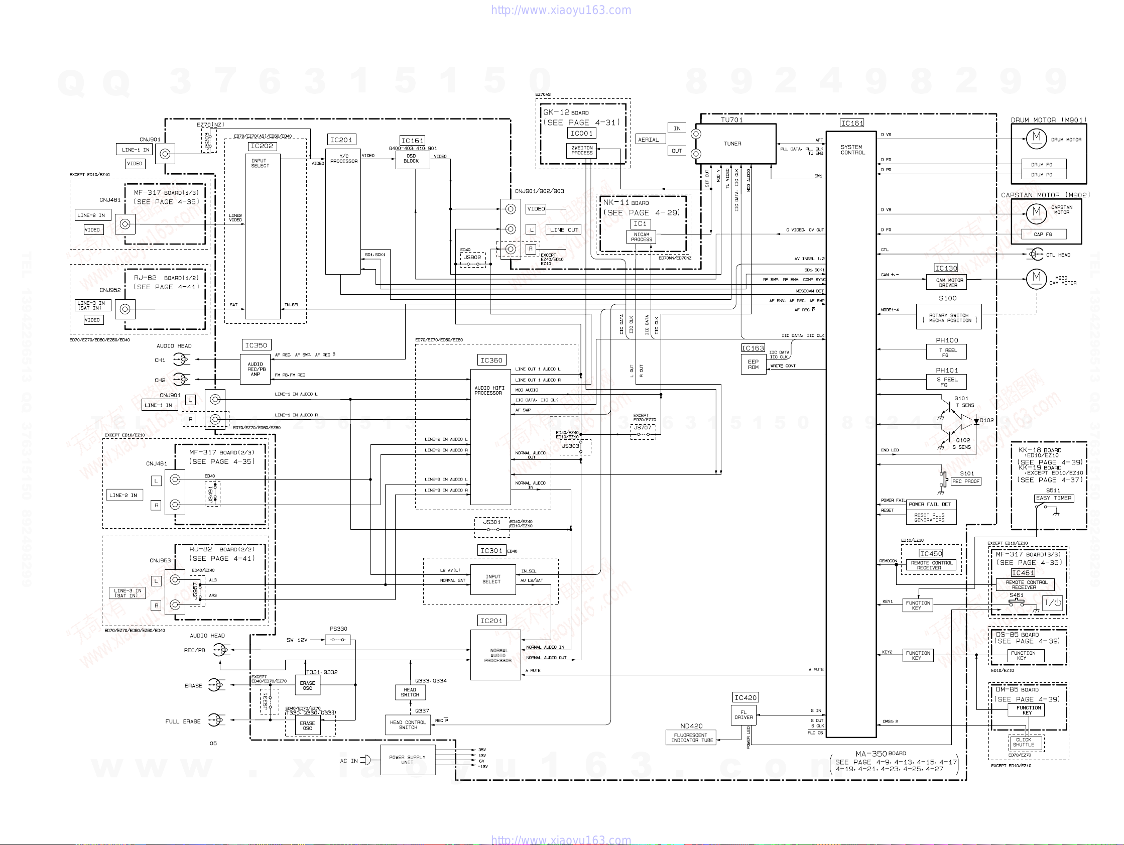
3-1. OVERALL BLOCK DIAGRAM
Q
Q
3
7
SECTION 3
BLOCK DIAGRAMS
6
3
1
5
1
5
0
8
9
SLV-ED10/ED40/ED60/ED70/EZ10/EZ40/EZ60/EZ70
2
4
9
8
2
9
9
TEL 13942296513 QQ 376315150 892498299
T
E
L
1
3
9
4
2
2
9
6
5
1
3
Q
Q
3
7
6
3
1
5
1
5
0
8
9
2
4
9
8
2
9
TEL 13942296513 QQ 376315150 892498299
9
w
w
w
.
x
i
a
3-1 3-2
o
y
u
1
6
3
.
c
o
m
SLV-ED10/ED40/ED60/ED70/EZ10/EZ40/EZ60/EZ70
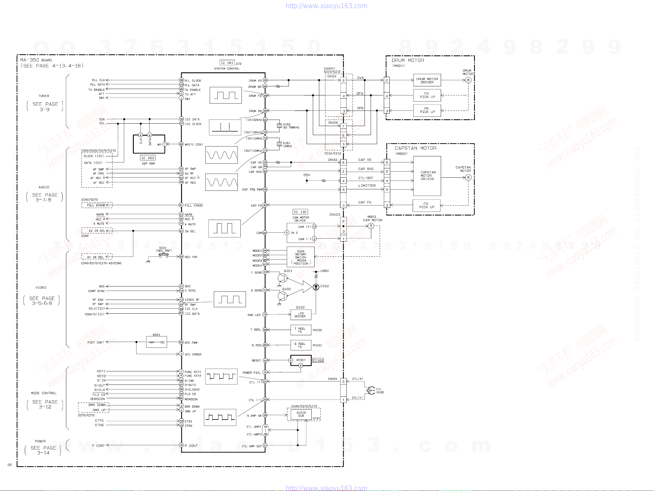
3-2. SERVO/SYSTEM CONTROL BLOCK DIAGRAM
Q
TEL 13942296513 QQ 376315150 892498299
Q
3
7
6
3
1
IC161 #• REC/PB
4.4Vp-p(2V)
IC161 #ª REC/PB
4.7Vp-p(2V)
IC161 &º REC/PB
2.1Vp-p(32.768kHz)
IC161 &£ REC/PB
5
1
5
0
8
9
2
4
9
8
2
9
9
TEL 13942296513 QQ 376315150 892498299
T
E
L
1
3
9
4
2
2
9
6
3.5Vp-p(10MHz)
IC161 $º REC/PB
4.9Vp-p(2V)
5
1
IC161 @¢ REC/PB
5.3Vp-p(2V)
3
Q
Q
3
7
6
3
1
5
1
5
0
8
9
2
4
9
8
2
9
9
w
w
w
IC161 #¡ REC
5.6Vp-p(2V)
IC161 #™ REC
5.6Vp-p(2V)
.
3-3 3-4
x
i
a
o
y
u
1
6
3
.
c
o
m
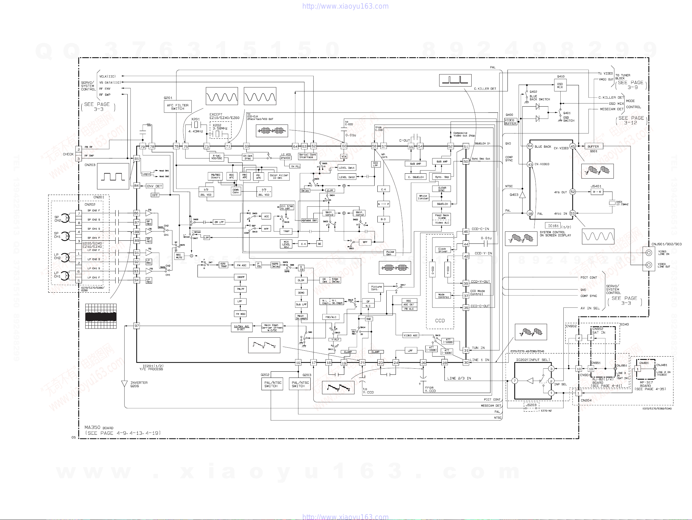
3-3. VIDEO BLOCK DIAGRAM
Q
Q
3
7
6
3
1
5
1
5
0
8
9
IC201 %º REC/PB
SLV-ED10/ED40/ED60/ED70/EZ10/EZ40/EZ60/EZ70
2
4
9
8
2
9
9
IC201 &∞ REC/PB
552mVp-p(4.433619MHz)
TEL 13942296513 QQ 376315150 892498299
IC201 *¡ REC/PB
5.2Vp-p(2V)
T
E
L
1
3
9
4
2
2
9
6
5
IC201 &¡ REC/PB
120mVp-p(3.579545MHz)
1
3
IC201 ^º REC/PB
REC:352mVp-p(H)
PB:552mVp-p(H)
Q
Q
IC201 %• REC/PB
7
3
6
3
1
5.4Vp-p(H)
5
1
5
0
IC161 $£ REC/PB
1.8Vp-p(H)
8
9
2
4
IC161 $∞ REC/PB
1.8Vp-p(H)
IC161 %£ REC/PB
3.4Vp-p(17.734475MHz)
8
9
2
9
TEL 13942296513 QQ 376315150 892498299
9
IC201 *• REC
1.4Vp-p(2V)
IC201 @¡ REC/PB
REC:360mVp-p(H)
PB:456mVp-p(H)
IC201 @§ REC/PB
REC:528mVp-p(H)
PB:624mVp-p(H)
REC:512mVp-p(H)
PB:608mVp-p(H)
IC201 #º REC
1.1Vp-p(H)
w
w
w
.
x
i
a
3-5 3-6
o
y
u
1
6
3
.
c
o
m
SLV-ED10/ED40/ED60/ED70/EZ10/EZ40/EZ60/EZ70
3-4. AUDIO BLOCK DIAGRAM
Q
Q
3
7
6
3
1
5
1
5
0
8
9
2
4
9
8
2
9
9
TEL 13942296513 QQ 376315150 892498299
T
E
L
1
3
9
4
2
2
9
6
5
1
3
Q
Q
3
7
6
3
1
5
1
5
0
8
9
2
4
9
8
2
9
TEL 13942296513 QQ 376315150 892498299
9
w
w
w
.
3-7 3-8
x
i
a
o
y
u
1
6
3
.
c
o
m
3-5. TUNER BLOCK DIAGRAM
Q
TEL 13942296513 QQ 376315150 892498299
Q
3
7
6
3
1
5
1
5
0
8
9
SLV-ED10/ED40/ED60/ED70/EZ10/EZ40/EZ60/EZ70
2
4
9
8
IC001 !∞ REC/PB
148mVp-p(4MHz)
2
9
9
TEL 13942296513 QQ 376315150 892498299
T
E
L
1
3
9
4
2
2
9
6
5
1
3
Q
Q
3
7
6
3
1
5
1
5
0
8
9
2
4
9
8
2
9
9
w
w
w
.
x
i
a
3-9 3-10
o
y
u
1
6
3
.
c
o
m
IC001 !§ REC/PB
740mVp-p(24.576MHz)
SLV-ED10/ED40/ED60/ED70/EZ10/EZ40/EZ60/EZ70
3-6. MODE CONTROL BLOCK DIAGRAM
Q
Q
3
7
6
3
1
5
1
5
0
8
9
2
4
9
8
2
9
9
TEL 13942296513 QQ 376315150 892498299
T
E
L
1
3
9
4
2
2
9
6
5
1
3
Q
Q
3
7
6
3
1
5
1
5
0
8
9
2
4
9
8
2
9
TEL 13942296513 QQ 376315150 892498299
9
w
w
w
.
3-11 3-12
x
i
a
o
y
u
1
6
3
.
c
o
m
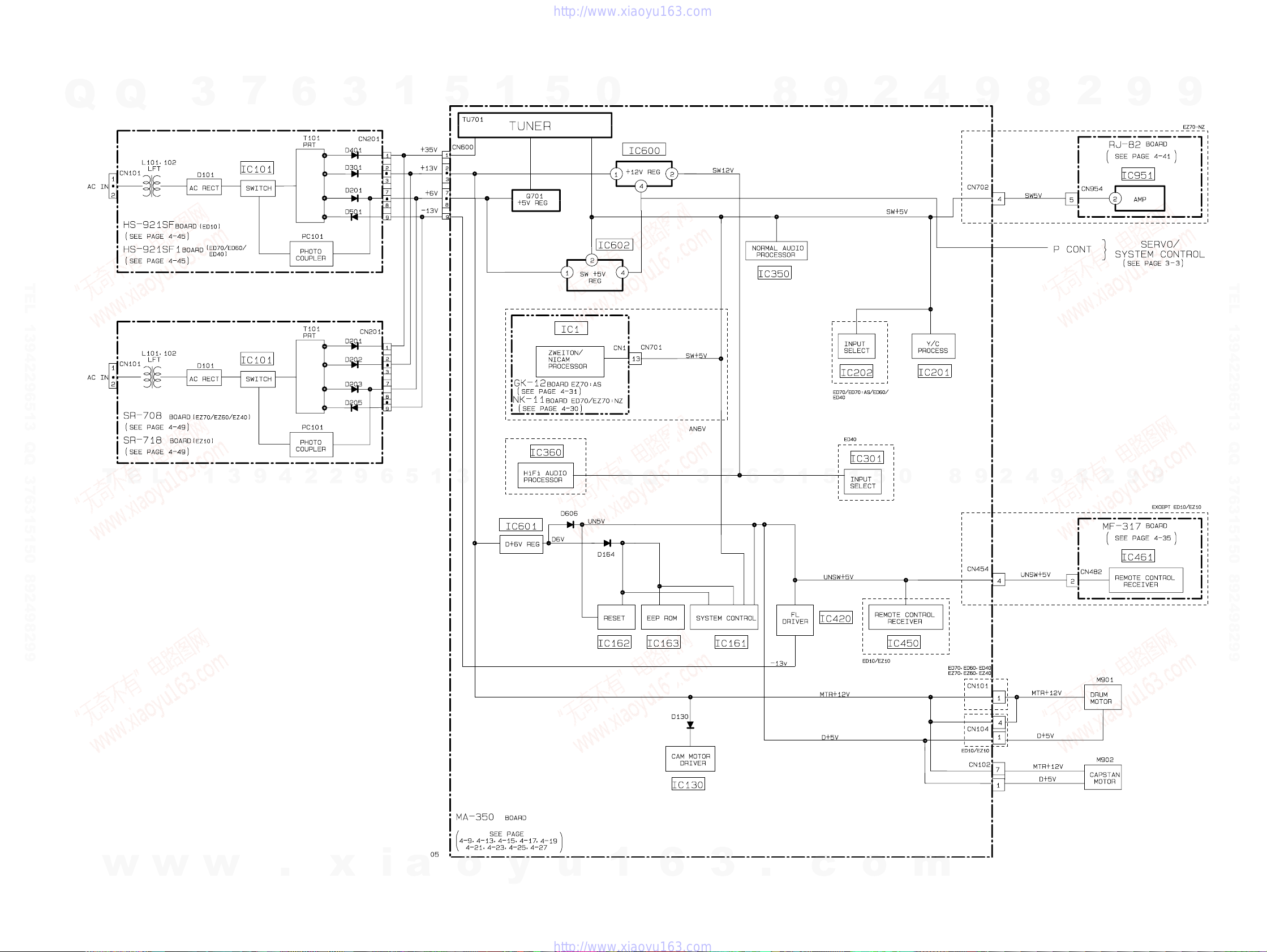
3-7. POWER BLOCK DIAGRAM
Q
Q
3
7
6
3
1
5
1
5
0
8
9
SLV-ED10/ED40/ED60/ED70/EZ10/EZ40/EZ60/EZ70
2
4
9
8
2
9
9
TEL 13942296513 QQ 376315150 892498299
T
E
L
1
3
9
4
2
2
9
6
5
1
3
Q
Q
3
7
6
3
1
5
1
5
0
8
9
2
4
9
8
2
9
TEL 13942296513 QQ 376315150 892498299
9
w
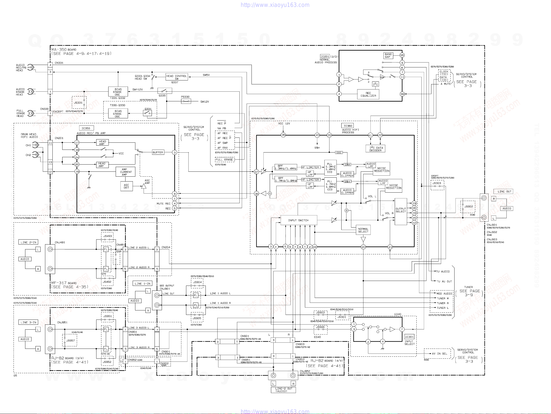
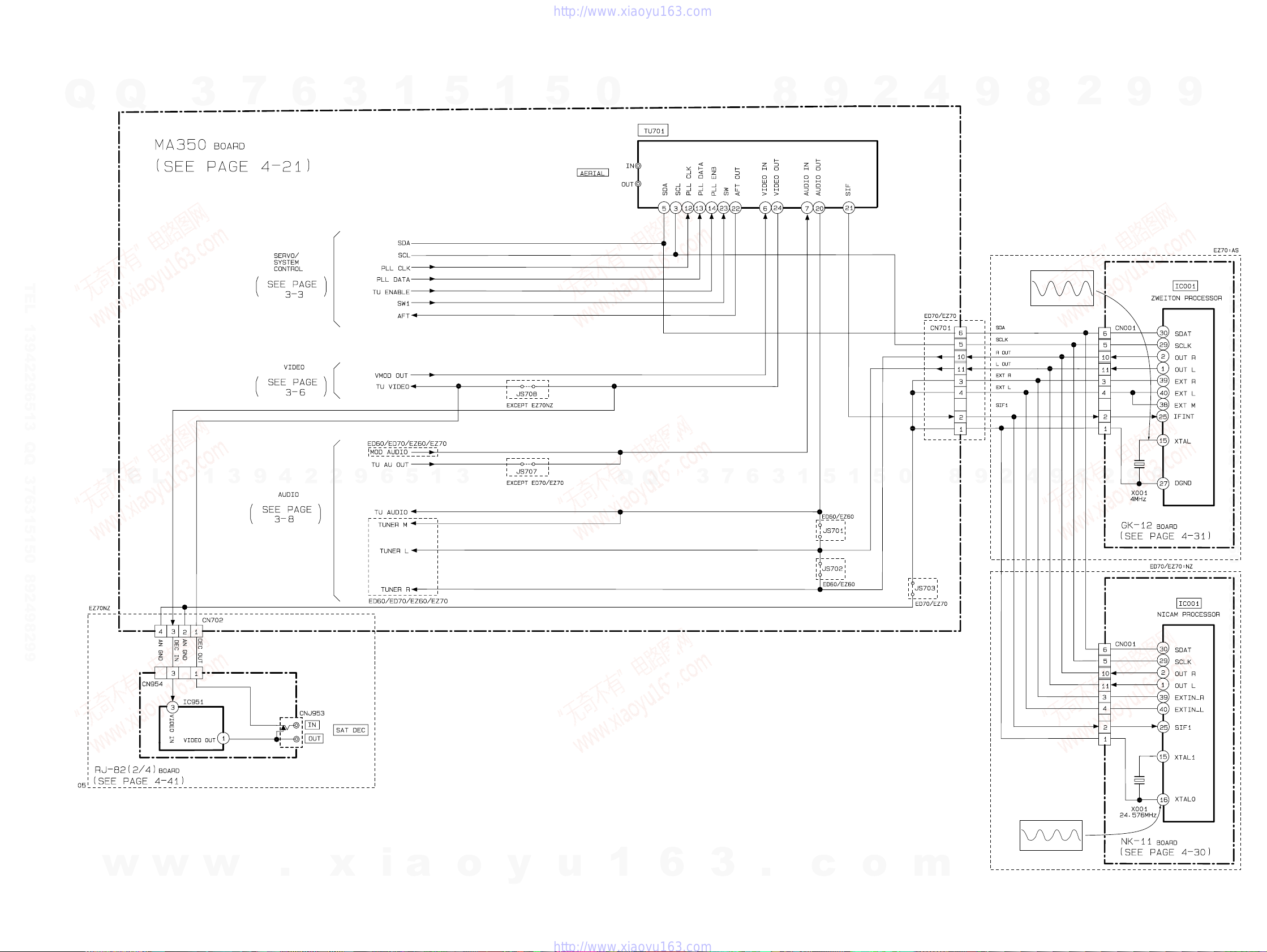
w
w
.
x
i
a
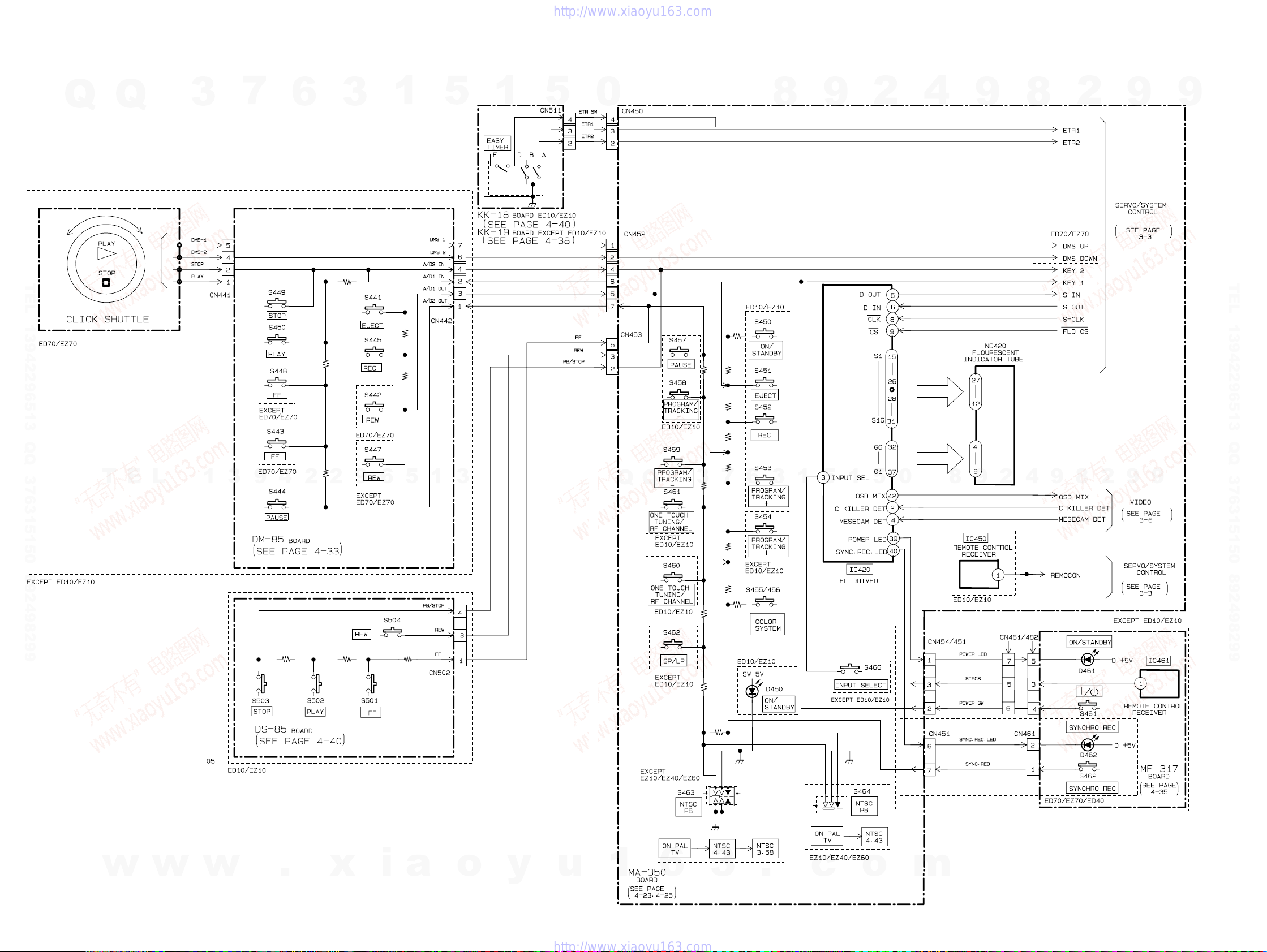
3-13 3-14 E
o
y
u
1
6
3
.
c
o
m

SLV-ED10/ED40/ED60/ED70/EZ10/EZ40/EZ60/EZ70
SECTION 4
PRINTED WIRING BOARDS AND SCHEMATIC DIA GRAMS
THIS NOTE IS COMMON FOR PRINTED WIRING
Q
TEL 13942296513 QQ 376315150 892498299
BOARDS AND SCHEMATIC DIAGRAMS.
Q
(In addition to this, the necessary mote is printed
in each block.)
For printed wiring board:
• X : indicates a lead wire mounted on the component
• x : indicates a lead wire mounted on the printed side.
• ® : Through hole.
• p : Parts mounted on the conductor side.
• b : Pattern from the side which enables seeing.
(The other layers’ patterns are not indicated.)
Caution:
Pattern face side: Parts on the pattern face side seen from
(Side B) the pattern face are indicated.
Parts face side: Parts on the parts face side seen from
(Side A) the parts face are indicated.
3
7
side.
6
3
1
5
1
5
0
For schematic Diagram:
• Caution when replacing chip parts.
New parts must be attached after removal of chip.
Be careful not to heat the minus side of tantalum capacitor,
because it is damaged by the heat.
• All resistors are in ohms, 1/
less otherwise specified.
kΩ : 1000Ω, MW : 1000kΩ.
• All capacitors are in µF unless otherwise noted. pF : µµF
50V or less are not indicated except for electrolytics and
tantalums.
• All variable and adjustable resistors have characteristic curve
B, unless otherwise noted.
• 2 : nonflammable resistor.
• 5 : fusible resistor.
• C : panel designation.
• ¢ : internal component.
• C : adjustment for repair.
• U : B+ Line.
• V : B– Line.
• Circled numbers refer to waveforms.
• Voltages are dc between measurement point.
• Readings are taken with a color-bar signal input.
• Readings are taken with a digital multimeter (DC 10MW).
• Voltage variations may be noted due to normal production
tolerances.
8
9
2
4
9
4
W (Chip resistors : 1/
8
2
9
10
W) un-
9
TEL 13942296513 QQ 376315150 892498299
TEL
13942296513
Q
Q
Note:The components identified by mark ! or dotted line
with mark ! are critical for safety.
Replace only with part number specified.
When indicating parts by reference
number, please include the board
name.
8
9
4
2
9
8
0
5
1
5
1
3
6
7
3
2
9
9
w
w
w
.
xia
o
y
u
1
6
4-1
3
.
c
o
m
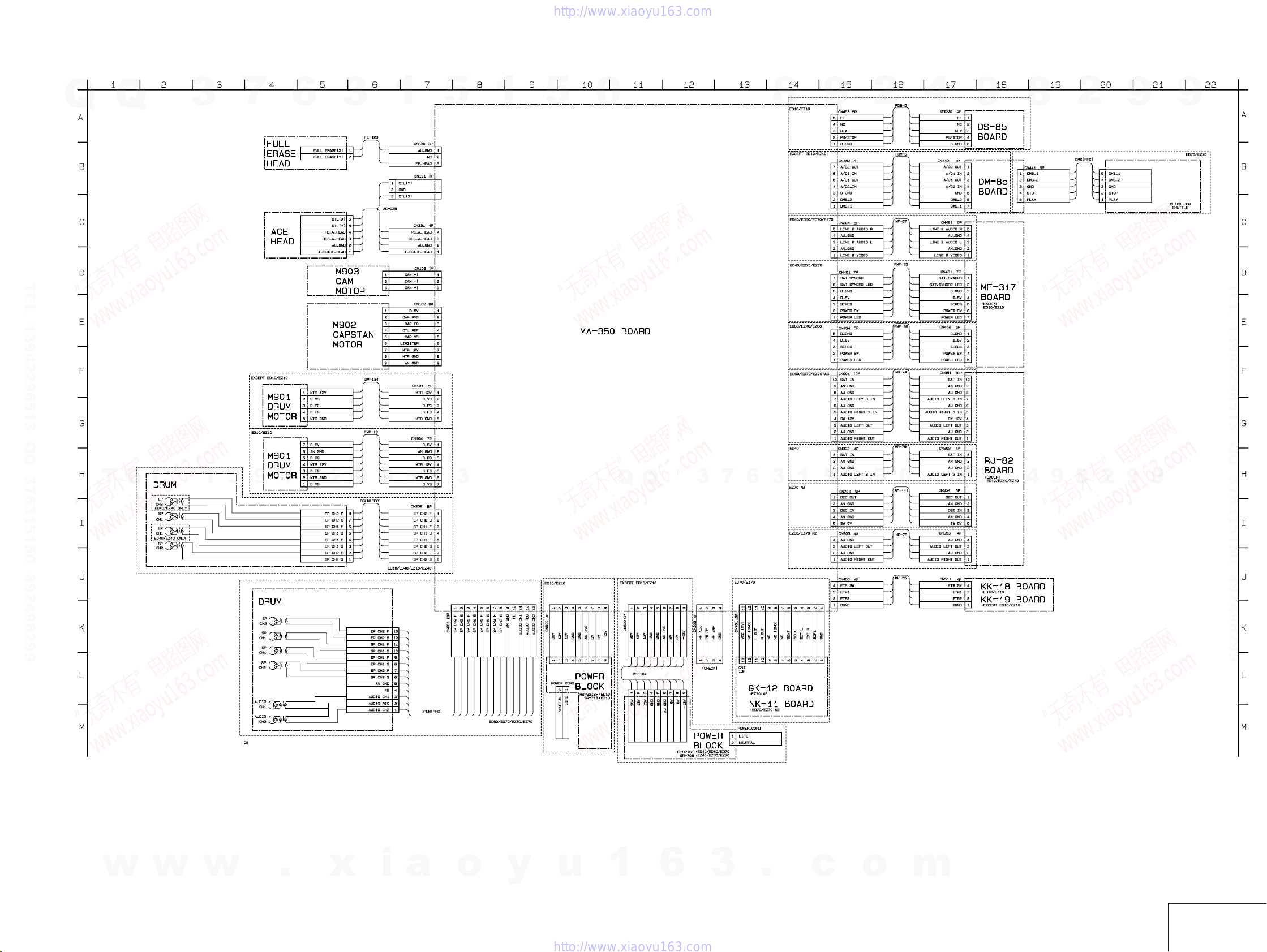
4-1. FRAME SCHEMATIC DIAGRAM
SLV-ED10/ED40/ED60/ED70/EZ10/EZ40/EZ60/EZ70
Q
TEL 13942296513 QQ 376315150 892498299
Q
3
7
6
3
1
5
1
5
0
8
9
2
4
9
8
2
9
9
TEL 13942296513 QQ 376315150 892498299
T
E
L
1
3
9
4
2
2
9
6
5
1
3
Q
Q
3
7
6
3
1
5
1
5
0
8
9
2
4
9
8
2
9
9
w
w
w
.
x
i
a
4-3 4-4
o
y
u
1
6
3
.
c
o
m
FRAME
 Loading...