

Page 1
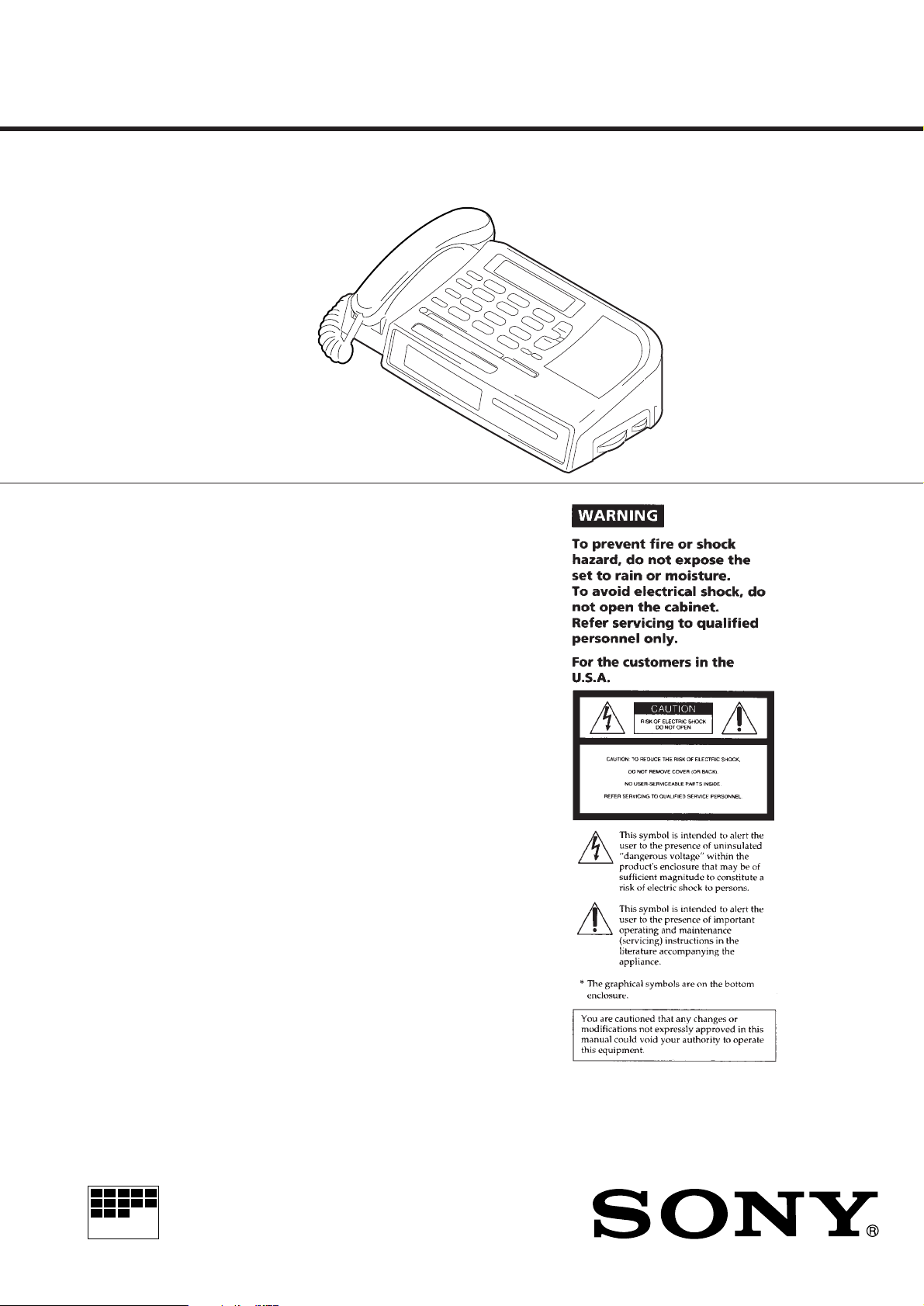
SCT-ID10
SERVICE MANUAL
Ver 1.0 1998.03
SPECIFICATIONS
Frequency range
FM : 87.5 – 108 MHz
AM :530 – 1,605 kHz
Speaker Approx. 6.6 cm (2 5/8 inches) dia., 8 ohms
Power output
100 mW (at 10% harmonic distortion)
Dial signal :
Tone, pulse selectable
Power requirements :
120V AC, 60Hz
For power backup :
9V DC, one 6F22 battery (Functions for clock radio only)
Battery life :
Approx. 35 hours using the Sony S-006P (U) battery
Dimensions :
Approx. 250 x 98.6 x 202 mm (w/h/d)
(9 7/8 x 4 x 8 inches) incl. projecting parts and controls
Mass Approx. 880g (2 lb. 31 oz) not incl. battery
Supplied accessories
Telephone line cord (1 )
Handset cord (1 )
US Model
Canadian Model
Design and specifications are subject to change without notice.
MICROFILM
ID TELEPHONE CLOCK RADIO
Page 2
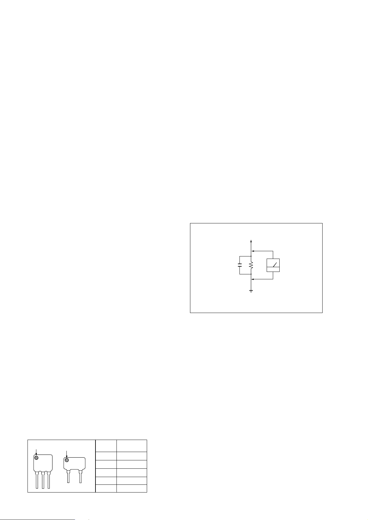
TABLE OF CONTENTS
SAFETY CHECK-OUT (US model)
Specifications ........................................................................... 1
1. GENERAL
Location and Function of Controls .................................... 3
2. DISASSEMBLY
2-1. Key Board, Cabinet (Upper) Assy Removal .............. 7
2-2. Main Board, Transformer Board, Transformer
retainer Board, Battery Blind Board Removal........... 7
2-3. Cabinet (Top) Removal .............................................. 8
Installation Power Cord .............................................. 8
3. DIAL POINTER INSTALLATION ............................ 9
4. TEST MODE................................................................. 10
5. ELECTRICAL ADJUSTMENTS............................11
6. DIAGRAMS
6-1. Explanation of IC Terminals..................................... 12
6-2. Block Diagram.......................................................... 13
6-3. Printed Wiring Boards (Main Section) ..................... 15
6-4. Schematic Diagram (Main Section) ......................... 17
6-5. Printed Wiring Boards (Key Section)....................... 19
6-6. Schematic Diagram (Key Section) ........................... 21
7. EXPLODED VIEWS
7-1. Base Unit Section ..................................................... 24
7-2. Handset Section ........................................................ 25
8. ELECTRICAL PARTS LIST.................................... 26
After correcting the original service problem, perform the
following safety check before releasing the set to the customer :
Check the antenna terminals, metal trim, “metallized” knobs,
screws, and all other exposed metal parts for AC leakage. Check
leakage as described below.
LEAKAGE TEST
The AC leakage from any exposed metal part to earth ground and
from all exposed metal parts to any exposed metal part having a
return to chassis, must not exceed 0.5mA (500 microampers).
Leakage current can be measured by any one of three methods.
1. A commercial leakage tester, such as the Simpson 229 or RCA
WT-540A. Follow the manufacturers’ instructions to use these
instruments.
2. A battery-operated AC milliammeter. The Data Precision 245
digital multimeter is suitable for this job.
3. Measuring the voltage drop across a resistor by means of a VOM
or battery-operated AC voltmeter . The “limit” indication is 0.75V,
so analog meters must have an accurate low-voltage scale. The
Simpson 250 and Sanwa SH-63Trd are examples of a passive
VOM that is suitable. Nearly all battery operated digital
multimeters that have a 2V AC range are suitable. (See Fig. A)
To Exposed Metal
Parts on Set
0.15
1.5k
µ
F
Ω
AC
voltmeter
(0.75V)
Notes on chip component replacement
• Never reuse a disconnected chip component.
• Notice that the minus side of a tantalum capacitor may be damaged by heat.
• HOW TO CHANGE THE CERAMIC FILTER
This model is used two ceramic filters of CF3 and CF1.
You must use same type of color marked ceramic filters in order
to meet same specifications.
Therefore, the ceramic filter must change two pieces together since
it’s supply two pieces in package as a spare parts.
mark
mark
Mark
Center
frequency
red 10.70MHz
CF3
CF1
blue 10.67MHz
orange 10.73MHz
black 10.64MHz
white 10.76MHz
Earth Ground
Fig. A. Using an AC voltmeter to check AC leakage.
SAFETY-RELATED COMPONENT WARNING!!
COMPONENTS IDENTIFIED BY MARK ! OR DOTTED LINE WITH
MARK ! ON THE SCHEMATIC DIAGRAMS AND IN THE PARTS
LIST ARE CRITICAL TO SAFE OPERATION.
REPLACE THESE COMPONENTS WITH SONY PARTS WHOSE
PART NUMBERS APPEAR AS SHOWN IN THIS MANUAL OR IN
SUPPLEMENTS PUBLISHED BY SONY.
ATTENTION AU COMPOSANT AYANT RAPPORT
À LA SÉCURITÉ!
LES COMPOSANTS IDENTIFIÉS P AR UNE MARQUE ! SUR LES
DIAGRAMMES SCHÉMA TIQUES ET LA LISTE DES PIÈCES SONT
CRITIQUES POUR LA SÉCURITÉ DE FONCTIONNEMENT. NE
REMPLACER CES COMPOSANTS QUE PAR DES PIÈCES SONY
DONT LES NUMÉROS SONT DONNÉS DANS CE MANUEL OU
DANS LES SUPPLÉMENTS PUBLIÉS PAR SONY.
– 2 –
Page 3
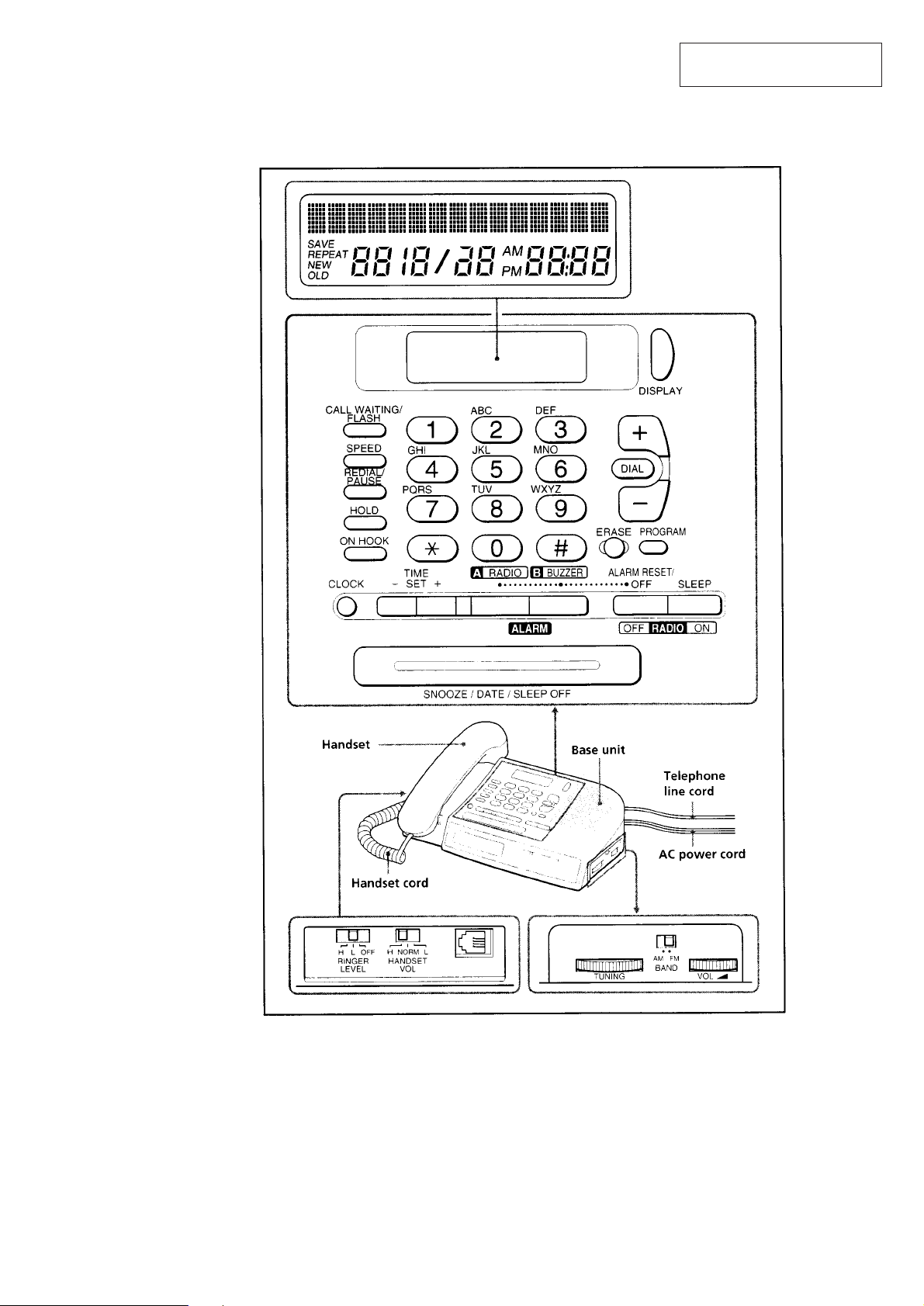
LOCATION AND FUNCTION OF CONTROLS
SECTION 1
GENERAL
This section is extracted from
instruction manual.
TONE
OPER
– 3 –
Page 4
– 4 –
Page 5
– 5 –
Page 6
– 6 –
Page 7
SECTION 2
)
y
DISASSEMBLY
Note : Follow the disassembly procedure in the numerical order given.
2-1. KEY BOARD, CABINET (UPPER) ASSY REMOVAL
Cabinet (Upper) assy
Rubber key switch
Key board
5
Screws
(+P 2.6x8)
CN101 (15 pin)
CN102 (7 pin)
3
Cabinet (Lower) assy
2
5
Screws (+P 2.6x8)
7
6
4
1
Screws (+P 3x14)
2-2. MAIN BOARD, TRANSFORMER BOARD, TRANSFORMER RETAINER BOARD,
BATTERY BLIND BOARD REMOVAL
1
Screws (+P3x14)
1
Screws (+P 3x14
9
Screws
(+BTP 2x8)
Buzzer
6
Remove solder
MAIN board
!º
4
4
4
5
7
Transformer board
8
Transformer retainer board
Power transformer
2
3
Screw (+P 2.6x8)
!¡
Battery blind board
Cabinet (Lower) ass
4
4
4
– 7 –
Page 8
2-3. CABINET (TOP) REMOVAL
)
)
3
Cabinet (top)
2
1
Screw (+BTP 3x10
INSTALLATION POWER CORD
1
2
4
Cabinet (bottom) assy
3
4
Power cord
Cabinet (Lower
Power transformer board
Battery blind board
– 8 –
Page 9

SECTION 3
DIAL POINTER INSTALLATION
Note : Follow the installation procedure in the numerical order given.
Marking (A)
A
Pointer
1
4
2
Knob (Vol)
3
Marking
Knob (tuning)
5
6
Turn the knob (VOL) to the
arrow direction fully
A
Making portion
of the knob (VOL)
within arrow A
marked area,
then attach it
4
Install the main board
2
Turn the shaft of CV1 to
the arrow direction fully
Cabinet (lower)
– 9 –
CV1
RV1
3
Turn the RV1 to the arrow direction fully
1
Turn the knob (tuning) to the
arrow direction fully
Knob
(tuning)
A
B
Page 10

SECTION 4
TEST MODE
1. Key Input Test
(1) Press the [PR OG] , [ERASE] , [*], [0], [#] buttons simultaneously .
(2) A beep tone sounds and test mode is now set.
(3) Press the [1] button to set the test mode to key input.
(4) A beep tone sounds each time the [CALLW AITIN/FLASH] , [SPEED] ,
[REDIAL/P AUSE] …… are pressed (order button is pressed does
not matter). Except for the [ONHOOK] button.
2. EEPROM Memory Test & Erasure
(1) Press the [PR OG] , [ERASE] , [*], [0], [#] buttons simultaneously .
(2) A beep tone sounds and test mode is now set.
(3) Press the [2] button to set the EEPROM test mode.
(4) A beep tone sounds, the message [EEPROMTESTING] appears
and testing starts.
3. LCD Test
(1) Press [3] button to set LCD test mode. All LCDs light up.
4. Power Failure Test
(1) Press the [PR OG] , [ERASE] , [*], [0], [#] buttons simultaneously .
(2) A beep tone sounds and test mode is now set.
(3) Remove the power cord from the plug socket (outlet) and plug
it back in once again. The following message appears on the
LCD display.
POWER FAIL OK
– 10 –
Page 11

SECTION 5
6
r
t
ELECTRICAL ADJUSTMENTS
TUNER SECTION
• RADIO switch : ON
• VOLUME : MIN
AM Section
BAND : AM
AM RF signal
generator
30% amplitude modulation by 400Hz
signal.
Output level : as low as possible
FM Section
BAND : FM
FM RF signal
generator
22.5kHz frequency deviation
by 400Hz signal.
Output level : as low as possible
Put the lead-wire
antenna close to
the set.
µ
8
Ω
0.01 F
L
level mete
• Repeat the procedures in each adjustment several times, and the
frequency coverage and tracking adjustments should be finally
done by the trimmer capacitors.
AM IF ALIGNMENT
Adjust for a maximum reading on level meter.
T1 455kHz
AM FREQUENCY COVERAGE ADJUSTMENT
Adjust for a maximum reading on level meter.
L4 520kHz
CT2 1,650kHz
AM TRACKING ADJUSTMENT
Adjust for a maximum reading on level meter.
L1 600kHz
CT1 1,400kHz
FM FREQUENCY COVERAGE ADJUSTMENT
Adjust for a maximum reading on level meter.
L3 86.5MHz
CT4 109.5MHz
FM TRACKING ADJUSTMENT
Adjust for a maximum reading on level meter.
confirmation 86.5MHz
CT3 109.5MHz
set
Adjustment Location :
[MAIN BOARD] (Component side)
speaker output
T1: AM IF Alignment
L1 : AM Tracking Adjustment
IC1
CT3 : FM Tracking Adjustment
CT1 : AM Tracking Adjustmen
L4 : AM Frequency
Coverage Adjustment
CT2 : AM Frequency Coverage Adjustment
L3 : FM Frequency Coverage Adjustment
CT4 : FM Frequency Coverage Adjustment
– 11 –
Page 12

SECTION 6
DIAGRAMS
6-1. EXPLANATION OF IC TERMINALS
IC602 TMP47C853F (SYSTEM CONTROL)
Pin No. Pin name I/O Description
1 DE O Data enable output terminal.
2 R/W O Read/write select signal output. 0 : Write, 1 : Read
3 RS O Register select signal output.
4 HOOK I Hook switch DET.
5 KO4 I Key return input.
6 KO5 I Key return input.
7 SP MUTE O Mute signal output.
8 AUTO INT I Auto initial DET terminal.
9 WT0 – Not used (“H” : Level).
10 STD I Dual tone alert signal delayed steering input.
11 XT IN – Not used (Open).
12 BELL I Ringer signal detect.
13 SCK O Serial clock output to EEPROM.
14 DATA I/O Serial data input/output terminal.
15 CS O Chip select output to EEPROM.
16 VSS – Ground.
17 NC – Not used (Open).
18 T TONE O Beep signal output.
19 DP O Dial pulse control signal output.
20 LINE CNT O Tel line control signal output.
21 TONE O DTMF signal output.
22 KO0 I Key return input.
23 KO1 I Key return input.
24 KO2 I Key return input.
25 KO3 I Key return input.
26 TEST I Test mode terminal. “L” : Normal
27 X IN I System clock oscillator (960kHz).
28 X OUT O System clock oscillator (960kHz).
29 RESET I System reset terminal.
30 HOLD I Power failuer DET terminal.
31 RADIO CNT O Radio signal output control.
32 BACK-UP I Back-up DET terminal.
33 DATA I Data input from IC301.
34 TEL MUTE O Mute signal output to speech network IC (IC101).
35 PH0 MUTE O Receiver signal mute output.
36 ALERT O FSK enable output.
37 TONE/PULSE I Tone/pulse select input terminal.
38 NC – Not used (Open).
39 VDD – Power supply (3V).
40 ROW 0 O Key source output.
41 ROW 1 O Key source output.
42 ROW 2 O Key source output.
43 ROW 3 O Key source output.
44 LCD RST O Reset signal output to LCD driver IC (IC604).
–––––––––––––––––
– 12 –
Page 13

6-2. BLOCK DIAGRAM
SCT-ID10
– 13 – – 14 –
• Signal path.
F : FM
N : RX (From Tel Line)
O : TX (To Tel Line)
P : bell
Page 14

SCT-ID10
r
SEMICONDUCTOR
LOCATION
Ref. No. Location
D1 I-9
D2 H-11
D3 H-10
D4 H-10
D5 E-8
D6 F-9
D7 F-9
D101 E-13
D102 E-13
D103 E-13
D104 E-13
D105 F-13
D106 E-13
D107 G-12
D108 G-13
D109 F-13
D110 F-6
D111(A) E-12
D111(B) I-4
D112 D-14
D201 E-14
6-3. PRINTED WIRING BOARDS (MAIN SECTION)
D202 F-14
D203 E-14
D204 E-14
D205 F-14
D206 D-15
D301 F-11
D302 H-11
D401 F-6
D501 E-10
D502 F-10
D503 E-12
D504 F-8
D505 E-10
IC1 F-4
IC2 H-9
IC101 H-5
IC104 F-6
IC201 F-14
IC301 H-13
Q1 G-4
Q2 E-5
Q3 E-8
Q101 F-13
Q102 F-13
Q103 G-13
Q104 F-12
Q105 G-12
Q106 F-7
Q401 F-6
Q501 E-10
Note:
• X : parts extracted from the component side.
• p : parts mounted on the conductor side.
• b : Pattern on the side which is seen.
– 15 – – 16 –
Page 15

6-4. SCHEMATIC DIAGRAM (MAIN SECTION)
p
r
Refer to page 23 for IC Block Diagrams.
SCT-ID10
Note:
• All capacitors are in µF unless otherwise noted. pF: µµF
50 WV or less are not indicated except for electrolytics
and tantalums.
• All resistors are in Ω and 1/
specified.
• ¢ : internal component.
Note: Note:
The components identi- Les composants identifiés
fied by mark ! or dotted par une marque ! sont criline with mark ! are cri- tiques pour la sécurité.
tical for safety. Ne les remplacer que par
Replace only with part une piéce portant le
number specified. numéro spécifié.
4
W or less unless otherwise
• U : B+ Line.
• H : adjustment for repair.
• Voltages and waveforms are dc with respect to ground
under no-signal (detuned) conditions.
no mark : FM (RADIO SECTION)
TALK (TELEPHONE SECTION)
( ) : AM (RADIO SECTION)
• V oltages are taken with a VOM (Input impedance 10 MΩ).
Voltage variations may be noted due to normal production tolerances.
• Waveforms are taken with a oscilloscope.
Voltage variations may be noted due to normal production tolerances.
• Circled numbers refer to waveforms.
• Signal path.
F : FM
N : RX (From Tel Line)
O : TX (To Tel Line)
P : bell
r
WA VEFORM
1
IC301 !º
0.2Vp-
0.34 µsec
VOLT/DIV : 0.1V AC
TIME/DIV : 0.2 µsec
– 17 – – 18 –
Page 16

SCT-ID10
r
SEMICONDUCTOR
LOCATION
Ref. No. Location
D601 I-13
D602 J-13
D603 J-14
D604 E-10
D605 E-11
D606 D-8
D607 D-9
D608 I-13
D609 B-13
D610 H-12
IC601 I-12
IC602 F-10
IC603 H-9
IC604 C-10
Q601 H-10
6-5. PRINTED WIRING BOARDS (KEY SECTION)
Note:
• X : parts extracted from the component side.
• p : parts mounted on the conductor side.
r
•
• b : Pattern from the side which enables seeing.
(The other layers' patterns are not indicated.)
Caution:
Pattern face side: Parts on the pattern face side seen from
(Conductor Side) the pattern face are indicated.
Parts face side: Parts on the parts face side seen from
(Component Side) the par ts face are indicated.
: Through hole.
• Caution when replacing chip parts.
New parts must be attached after removal of chip.
Be careful not to heat the minus side of tantalum capacitor, because it is damaged by the heat.
– 19 – – 20 –
Page 17

6-6. SCHEMATIC DIAGRAM (KEY SECTION)
p
r
Refer to page 23 for IC Block Diagrams.
SCT-ID10
Note:
• All capacitors are in µF unless otherwise noted. pF: µµF
50 WV or less are not indicated except for electrolytics
and tantalums.
• All resistors are in Ω and 1/
specified.
¢
•
• U : B+ Line.
• Voltages and waveforms are dc with respect to ground
: internal component.
under no-signal conditions.
no mark : FM (RADIO SECTION)
4
W or less unless otherwise
r
WA VEFORM
• V oltages are taken with a VOM (Input impedance 10 MΩ).
Voltage variations may be noted due to normal production tolerances.
• Waveforms are taken with a oscilloscope.
Voltage variations may be noted due to normal production tolerances.
• Circled numbers refer to waveforms.
1
0.6Vp-
1 µsec
IC602 @
VOLT/DIV : 0.2V AC
TIME/DIV : 0.5 µsec
– 21 – – 22 –
Page 18

E
r
d
IC BLOCK DIAGRAMS
IC101 BA6566
TO
18 17 16 15 14 13 12 11 10
VL
AGC
TRANSMIT
TC
TI 1
MIC
PRE
TI 2
10k 10k
VB
10k
DTMF
PRE
MF
10k
MU
MUTE
INTERFACE
R1
VBVB
10k
RCV
PRE
SECTION 7
EXPLODED VIEWS
NOTE :
RC
AT
• -XX, -X mean standardized parts, so they
may have some difference from the original
one.
VB
• Items marked “ * ”are not stocked since they
are seldom required for routine service. Some
10k
10k
delay should be anticipated when ordering
these items.
AT
10k
PRE
7-1. BASE UNIT SECTION
• The mechanical parts with no reference
number in the exploded views are not
supplied.
• Hardware (# mark) list and accessories and
packing materials are given in the last of this
parts list.
The components identified by mark !
or dotted line with mark ! are critical
for safety.
Replace only with part number specified.
Les composants identifiés par une
marque ! sont critiques pour la sécurité.
Ne les remplacer que par une pièce
portant le numéro spécifié.
AGC
POWER
DISSIPATION
123456789
GND
RL
CL
VL
IC201 BA8206
VCC
RSL
LFO
1
POWER
SUPPLY
2
WITH
HYSTERISIS
LFI
3
LOW
FREQ.
OSC
4
HIGH
FREQ.
OSC
AMP
OUT
8
HFI
7
6
HFO
GND
5
IN+
IN–
VREF
CAP
TRIGIN
TRIGRC
TRIGOUT
MODE
OSCIN
OSCOUT
VSS
LINE
CURRENT
SENSE
LINE CONTROL
PDC
IC301 MT88E43ASR
1
+
ANTI-ALIAS
–
2
GS
3
INTERNAL
4
GENERATOR
5
6
7
8
9
10
11
FILTER
TO
CCT
BIAS
OSCILLATOR
AGC
TO
INTERNAL
CCT
VB
VREG
ALERT SIGNAL
HIGH TONE
FILTER
ALERT SIGNAL
LOW TONE
FILTER
FSK
BANDPASS
FILTER
Vcc
CARRIER
DETECTOR
FSK
DEMODUL-
ATOR
RO 1
TONE
DETECTION
ALGORITHM
GENERATOR
RECOVERY
POW
INTERRUPT
DATA
TIMING
GUARD
TIME
RO 2
RECIEVE
24
VDD
ST/GT
23
22
EST
STD
21
INT
20
19
CD
18
DR
DATA
17
DCLK
16
FSKEN
15
14
PWDN
IC
1312
#2
6
5
D1
#1
T2
7
8
9
W52
22
4
19
3
18
17
2
16
SP1
BZ201
J102
LCD
601
20
21
10
11
12
23
24
13
1
#1
#1
#1
17
#2
#2
15
14
r
CIRCUIT BOARDS LOCATION
D1
MAIN board
Ref. No. Part No. Description Remark Ref. No. Part No. Description Remark
* 1 A-3679-977-A KEY BOARD, COMPLETE
MICROCOMPUTER board
TRANSFORMER board
2 1-771-368-11 SWITCH, RUBBER KEY
3 3-021-131-01 BUTTON (CLOCK)
4 3-021-129-01 PLATE (CLOCK), TRANSPARENT
5 1-696-455-71 CORD, CURL
* 18 3-021-138-01 PLATE (LCD), SHIELD
6 X-3375-548-1 CABINET (UPPER) ASSY
* 7 1-668-384-11 TRANSFORMER BOARD
* 8 1-669-395-11 TRANSFORMER RETAINER BOARD
* 23 1-669-397-11 BATTERY BLIND BOARD
! 24 1-769-339-22 CORD, POWER
* 9 A-3679-978-A MAIN BOARD, COMPLETE
10 3-922-000-01 KNOB (TUNING)
11 3-922-002-11 POINTER
TRANSFORMER RETAINER boar
12 3-919-268-01 KNOB (VOL)
13 3-021-128-01 CABINET (LOWER)
BATTERY BLIND board
14 3-369-135-21 LID, BATTERY CASE
15 3-368-852-01 FOOT
! T2 1-429-460-11 TRANSFORMER, POWER
16 3-021-134-01 HOLDER, LCD
– 23 – – 24 –
17 1-694-420-11 CONDUCTIVE BOARD, CONNECTION
19 3-021-132-01 BUTTON (TEL)
20 3-371-765-21 SCREW (2X8), +BTP
21 3-021-133-01 HOOK
22 1-777-242-11 CORD, CONNECTION
BZ201 1-505-978-11 PIEZOELECTRIC BUZZER
D1 1-810-027-11 DIODE SL-2994-54TB (DATE DISPLAY)
J102 1-770-504-11 JACK, MODULAR (TO HANDSET)
LCD601 1-803-112-11 DISPLAY PANEL, LIQUID CRYSTAL
SP1 1-504-748-21 SPEAKER (6.6cm)
W52 1-535-804-21 SNAP, BATTERY
Page 19

7-2. HAMDSET SECTION
52
#1
53
#1
55
MIC1
SP2
54
56
#2
51
Ref. No. Part No. Description Remark Ref. No. Part No. Description Remark
51 3-021-136-01 HAND SET (LOWER)
52 3-021-135-01 HAND SET (UPPER)
* 53 3-021-137-01 WEIGHT
54 3-380-401-01 SPACER (SPEAKER)
* 55 1-669-396-11 MICROPHONE RETAINER BOARD
56 1-770-505-11 JACK,MODULAR
MIC1 1-542-161-11 MICROPHONE, ELECTRET CONDENSER
SP2 1-550-648-11 RECEIVER, DYNAMIC
– 25 –
Page 20

SECTION 8
KEY
NOTE :
• Due to standardization, replacements in the
parts list may be different from the parts
specified in the diagrams or the components
used on the set.
• -XX, -X mean standardized parts, so they
may have some difference from the original
one.
• RESISTORS
All resistors are in ohms
METAL : Metal-film resistor
METAL OXIDE :Metal oxide-film resistor
F : nonflammable
• Items marked “ * ”are not stocked since
they are seldom required for routine service.
Some delay should be anticipated when
ordering these items.
Ref. No. Part No. Description Remark Ref. No. Part No. Description Remark
* A-3679-977-A KEY BOARD, COMPLETE
*******************
1-694-420-11 CONDUCTIVE BOARD, CONNECTION
3-021-134-01 HOLDER, LCD
* 3-021-138-01 PLATE (LCD), SHIELD
< CAPACITOR >
C601 1-126-918-11 ELECT 4700uF 20% 6.3V
C602 1-163-038-11 CERAMIC CHIP 0.1uF 25V
C603 1-163-037-11 CERAMIC CHIP 0.022uF 10% 25V
C604 1-163-251-11 CERAMIC CHIP 100PF 5% 50V
C605 1-163-251-11 CERAMIC CHIP 100PF 5% 50V
C606 1-164-505-11 CERAMIC CHIP 2.2uF 16V
C607 1-163-038-11 CERAMIC CHIP 0.1uF 25V
C608 1-126-964-11 ELECT 10uF 20% 50V
C609 1-135-181-21 TANTALUM CHIP 4.7uF 20% 6.3V
C610 1-135-181-21 TANTALUM CHIP 4.7uF 20% 6.3V
C611 1-135-259-11 TANTAL. CHIP 10uF 20% 6.3V
C612 1-164-232-11 CERAMIC CHIP 0.01uF 50V
C613 1-101-001-00 CERAMIC 0.001uF 50V
< DIODE >
D601 8-719-941-09 DIODE DAP202U
D602 8-719-941-09 DIODE DAP202U
D603 8-719-109-89 DIODE RD5.6ESB2
D604 8-719-988-82 DIODE RB715F
D605 8-719-988-82 DIODE RB715F
D606 8-719-988-82 DIODE RB715F
D607 8-719-988-82 DIODE RB715F
D608 8-719-991-09 LED SLP381F-51-A (LCD BACK-LIGHT)
D609 8-719-991-09 LED SLP381F-51-A (LCD BACK-LIGHT)
D610 8-719-941-86 DIODE DAN202U
< IC >
IC601 8-759-440-91 IC S-80723SL-AL-T1
IC602 8-759-529-21 IC TMP47C853F-K247
IC603 8-759-535-04 IC BR93LC56F-E2
IC604 8-759-529-23 IC NJU6469LFG1
< LIQUID CRYSTAL DISPLAY >
LCD601 1-803-112-11 DISPLAY PANEL, LIQUID CRYSTAL
ELECTRICAL PARTS LIST
• SEMICONDUCTORS
In each case, u : µ , for example :
uA.... : µ A.... , uPA.... : µ PA....
uPB.... : µ PB.... , uPC.... : µPC....
uPD.... : µ PD....
• CAPACITORS
uF : µ F
• COILS
uH : µ H
Q601 8-729-620-06 TRANSISTOR 2SC3052-EF
R601 1-216-105-11 RES,CHIP 220K 5% 1/10W
R602 1-216-105-11 RES,CHIP 220K 5% 1/10W
R604 1-216-073-00 METAL CHIP 10K 5% 1/10W
R606 1-216-073-00 METAL CHIP 10K 5% 1/10W
R607 1-216-073-00 METAL CHIP 10K 5% 1/10W
R608 1-216-073-00 METAL CHIP 10K 5% 1/10W
R609 1-216-065-11 RES,CHIP 4.7K 5% 1/10W
R610 1-216-073-00 METAL CHIP 10K 5% 1/10W
R611 1-216-105-11 RES,CHIP 220K 5% 1/10W
R612 1-216-105-11 RES,CHIP 220K 5% 1/10W
R613 1-216-073-00 METAL CHIP 10K 5% 1/10W
R615 1-216-025-11 RES,CHIP 100 5% 1/10W
R616 1-216-025-11 RES,CHIP 100 5% 1/10W
R617 1-216-025-11 RES,CHIP 100 5% 1/10W
R618 1-216-025-11 RES,CHIP 100 5% 1/10W
R619 1-216-093-00 METAL CHIP 68K 5% 1/10W
R620 1-216-093-00 METAL CHIP 68K 5% 1/10W
R621 1-216-049-11 RES,CHIP 1K 5% 1/10W
R622 1-216-105-11 RES,CHIP 220K 5% 1/10W
R623 1-216-105-11 RES,CHIP 220K 5% 1/10W
R624 1-216-105-11 RES,CHIP 220K 5% 1/10W
R625 1-216-105-11 RES,CHIP 220K 5% 1/10W
R626 1-216-025-11 RES,CHIP 100 5% 1/10W
R627 1-216-105-11 RES,CHIP 220K 5% 1/10W
R628 1-216-105-11 RES,CHIP 220K 5% 1/10W
R629 1-216-105-11 RES,CHIP 220K 5% 1/10W
R630 1-216-105-11 RES,CHIP 220K 5% 1/10W
R631 1-216-105-11 RES,CHIP 220K 5% 1/10W
R632 1-216-105-11 RES,CHIP 220K 5% 1/10W
R633 1-216-105-11 RES,CHIP 220K 5% 1/10W
R634 1-216-105-11 RES,CHIP 220K 5% 1/10W
R636 1-216-085-00 METAL CHIP 33K 5% 1/10W
R637 1-216-101-00 METAL CHIP 150K 5% 1/10W
R638 1-216-097-11 METAL CHIP 100K 5% 1/10W
X601 1-567-902-11 OSCILLATOR, CERAMIC (960kHz)
************************************************************
The components identified by mark !
or dotted line with mark ! are critical
for safety.
Replace only with part number specified.
Les composants identifiés par une
marque ! sont critiques pour la sécurité.
Ne les remplacer que par une pièce
portant le numéro spécifié.
When indicating parts by reference number, please include the board.
< TRANSISTOR >
< RESISTOR >
< VIBRATOR >
– 26 –
Page 21

MAIN
Ref. No. Part No. Description Remark Ref. No. Part No. Description Remark
* A-3679-978-A MAIN BOARD, COMPLETE
********************
1-535-804-21 SNAP, BATTERY
1-769-339-22 CORD, POWER
1-777-242-11 CORD, CONNECTION
< CAPACITOR >
C1 1-163-227-11 CERAMIC CHIP 10PF 0.5PF 50V
C2 1-163-227-11 CERAMIC CHIP 10PF 0.5PF 50V
C3 1-163-102-00 CERAMIC CHIP 24PF 5% 50V
C5 1-163-088-00 CERAMIC CHIP 5PF 50V
C6 1-163-251-11 CERAMIC CHIP 100PF 5% 50V
C7 1-163-106-00 CERAMIC CHIP 36PF 5% 50V
C8 1-163-235-11 CERAMIC CHIP 22PF 5% 50V
C9 1-163-099-00 CERAMIC CHIP 18PF 5% 50V
C10 1-164-232-11 CERAMIC CHIP 0.01uF 50V
C11 1-128-551-11 ELECT 22uF 20% 25V
C12 1-163-031-11 CERAMIC CHIP 0.01uF 50V
C13 1-126-160-11 ELECT 1uF 20% 50V
C15 1-163-038-11 CERAMIC CHIP 0.1uF 25V
C16 1-163-031-11 CERAMIC CHIP 0.01uF 50V
C17 1-126-963-11 ELECT 4.7uF 20% 50V
C18 1-126-964-11 ELECT 10uF 20% 50V
C19 1-163-809-11 CERAMIC CHIP 0.047uF 10% 25V
C20 1-164-346-11 CERAMIC CHIP 1uF 16V
C21 1-128-551-11 ELECT 22uF 20% 25V
C22 1-126-934-11 ELECT 220uF 20% 10V
C23 1-164-346-11 CERAMIC CHIP 1uF 16V
C24 1-164-346-11 CERAMIC CHIP 1uF 16V
C25 1-126-934-11 ELECT 220uF 20% 10V
C26 1-164-346-11 CERAMIC CHIP 1uF 16V
C27 1-164-346-11 CERAMIC CHIP 1uF 16V
C28 1-163-009-11 CERAMIC CHIP 0.001uF 10% 50V
C29 1-163-017-00 CERAMIC CHIP 0.0047uF 5% 50V
C30 1-163-038-11 CERAMIC CHIP 0.1uF 25V
C31 1-163-009-11 CERAMIC CHIP 0.001uF 10% 50V
C32 1-163-009-11 CERAMIC CHIP 0.001uF 10% 50V
C33 1-164-346-11 CERAMIC CHIP 1uF 16V
C34 1-164-232-11 CERAMIC CHIP 0.01uF 50V
C35 1-163-031-11 CERAMIC CHIP 0.01uF 50V
C36 1-163-031-11 CERAMIC CHIP 0.01uF 50V
C37 1-163-031-11 CERAMIC CHIP 0.01uF 50V
C38 1-126-925-11 ELECT 470uF 20% 10V
C39 1-126-926-11 ELECT 1000uF 20% 10V
C40 1-126-934-11 ELECT 220uF 20% 16V
C41 1-163-031-11 CERAMIC CHIP 0.01uF 50V
C42 1-163-031-11 CERAMIC CHIP 0.01uF 50V
C43 1-163-009-11 CERAMIC CHIP 0.001uF 10% 50V
C44 1-163-205-00 CERAMIC CHIP 0.001uF 5% 50V
C45 1-163-205-00 CERAMIC CHIP 0.001uF 5% 50V
C101 1-164-232-11 CERAMIC CHIP 0.01uF 50V
C102 1-126-961-11 ELECT 2.2uF 20% 50V
C103 1-126-966-11 ELECT 33uF 20% 35V
C104 1-126-961-11 ELECT 2.2uF 20% 50V
C105 1-128-551-11 ELECT 22uF 20% 25V
C106 1-126-964-11 ELECT 10uF 20% 50V
C107 1-126-925-11 ELECT 470uF 20% 10V
C108 1-163-005-11 CERAMIC CHIP 470PF 10% 50V
C109 1-163-005-11 CERAMIC CHIP 470PF 10% 50V
C110 1-163-038-11 CERAMIC CHIP 0.1uF 25V
C111 1-163-012-00 CERAMIC CHIP 0.0018uF 10% 50V
C112 1-163-007-11 CERAMIC CHIP 680PF 10% 50V
C113 1-163-017-00 CERAMIC CHIP 0.0047uF 5% 50V
C114 1-163-809-11 CERAMIC CHIP 0.047uF 10% 25V
C115 1-163-809-11 CERAMIC CHIP 0.047uF 10% 25V
C116 1-163-003-11 CERAMIC CHIP 330PF 10% 50V
C117 1-163-017-00 CERAMIC CHIP 0.0047uF 5% 50V
C118 1-164-004-11 CERAMIC CHIP 0.1uF 10% 25V
C119 1-163-017-00 CERAMIC CHIP 0.0047uF 5% 50V
C120 1-163-005-11 CERAMIC CHIP 470PF 10% 50V
C121 1-164-232-11 CERAMIC CHIP 0.01uF 50V
C122 1-163-005-11 CERAMIC CHIP 470PF 10% 50V
C123 1-163-035-00 CERAMIC CHIP 0.047uF 50V
C124 1-163-038-11 CERAMIC CHIP 0.1uF 25V
C125 1-164-505-11 CERAMIC CHIP 2.2uF 16V
C126 1-164-004-11 CERAMIC CHIP 0.1uF 10% 25V
C127 1-126-964-11 ELECT 10uF 20% 50V
C128 1-163-038-11 CERAMIC CHIP 0.1uF 25V
C129 1-163-035-00 CERAMIC CHIP 0.047uF 50V
C130 1-163-038-11 CERAMIC CHIP 0.1uF 25V
C131 1-164-004-11 CERAMIC CHIP 0.1uF 10% 25V
C201 1-137-479-11 FILM 1uF 5% 250V
C202 1-126-963-11 ELECT 4.7uF 20% 50V
C203 1-126-957-11 ELECT 0.22uF 20% 50V
C204 1-163-017-00 CERAMIC CHIP 0.0047uF 5% 50V
C205 1-126-956-11 ELECT 0.1uF 20% 50V
C301 1-102-244-00 CERAMIC 220PF 10% 500V
C302 1-102-244-00 CERAMIC 220PF 10% 500V
C303 1-163-038-11 CERAMIC CHIP 0.1uF 25V
C304 1-163-038-11 CERAMIC CHIP 0.1uF 25V
C305 1-126-934-11 ELECT 220uF 20% 10V
C401 1-164-505-11 CERAMIC CHIP 2.2uF 16V
C402 1-126-964-11 ELECT 10uF 20% 50V
C501 1-126-934-11 ELECT 220uF 20% 16V
C502 1-126-934-11 ELECT 220uF 20% 16V
C503 1-126-967-11 ELECT 47uF 20% 10V
C504 1-163-031-11 CERAMIC CHIP 0.01uF 50V
C505 1-126-964-11 ELECT 10uF 20% 50V
C506 1-126-925-11 ELECT 470uF 20% 10V
C507 1-163-031-11 CERAMIC CHIP 0.01uF 50V
C508 1-126-934-11 ELECT 220uF 20% 16V
< FILTER >
CF1 1-579-632-51 FILTER, CERAMIC
CF2 1-577-072-11 FILTER, CERAMIC
CF3 1-579-632-51 FILTER, CERAMIC
< CONNECTOR >
* CN1 1-691-573-11 PIN, CONNECTOR (PC BOARD) 2P
CN101 1-573-209-11 SOCKET, CONNECTOR 15P
* CN102 1-568-273-11 SOCKET, CONNECTOR 7P
< TRIMMER >
CT1 1-151-673-11 CAP, VARIABLE (TUNING)
– 27 –
Page 22

MAIN
Ref. No. Part No. Description Remark Ref. No. Part No. Description Remark
CT2 1-151-673-11 CAP, VARIABLE (TUNING)
CT3 1-151-673-11 CAP, VARIABLE (TUNING)
CT4 1-151-673-11 CAP, VARIABLE (TUNING)
< VARIABLE CAPACITOR >
CV1 1-151-673-11 CAP, VARIABLE (TUNING)
< DIODE >
D1 1-810-027-11 DIODE SL-2994-54TB
D2 8-719-911-19 DIODE 1SS119
D3 8-719-911-19 DIODE 1SS119
D4 8-719-109-85 DIODE RD5.1ES-B2
D5 8-719-911-19 DIODE 1SS119
D6 8-719-911-19 DIODE 1SS119
D7 8-719-052-88 DIODE 1N4002
D101 8-719-970-02 DIODE 1SR139-400
D102 8-719-970-02 DIODE 1SR139-400
D103 8-719-970-02 DIODE 1SR139-400
D104 8-719-970-02 DIODE 1SR139-400
D105 8-719-991-33 DIODE 1SS133T-77
D106 8-719-050-84 DIODE RB441Q-40T-77
D107 8-719-991-33 DIODE 1SS133T-77
D108 8-719-109-85 DIODE RD5.1ES-B2
D109 8-719-160-59 DIODE RD13F-B2
D110 8-719-991-33 DIODE 1SS133T-77
D111(A) 8-719-991-33 DIODE 1SS133T-77
D111(B) 8-719-109-97 DIODE RD6.8ES-B2
D112 8-719-991-33 DIODE 1SS133T-77
D201 8-719-970-02 DIODE 1SR139-400
D202 8-719-970-02 DIODE 1SR139-400
D203 8-719-970-02 DIODE 1SR139-400
D204 8-719-970-02 DIODE 1SR139-400
D205 8-719-983-97 DIODE MTZJ-T-72-39B
D206 8-719-991-33 DIODE 1SS133T-77
D301 8-719-991-33 DIODE 1SS133T-77
D302 8-719-991-33 DIODE 1SS133T-77
D401 8-719-991-33 DIODE 1SS133T-77
D501 8-719-052-88 DIODE 1N4002
D502 8-719-109-97 DIODE RD6.8ES-B2
D503 8-719-983-66 DIODE MTZJ-T-72-3.6B
D504 8-719-109-63 DIODE RD3.0ESB2
D505 8-719-052-88 DIODE 1N4002
D506 8-719-983-66 DIODE MTZJ-T-72-3.6B
< FILTER >
T101 1-424-024-11 FILTER, NOISE
< IC >
IC1 8-752-037-02 IC CXA1019S
IC2 8-759-193-05 IC LC85632
IC101 8-759-979-34 IC BA6566
IC104 8-759-921-81 IC SN74HC4066N
IC201 8-759-081-73 IC BA8206
IC301 8-759-529-22 IC MT88E43ASR
< JACK >
J101 1-770-503-11 JACK, MODULAR (2C) 6P (LINE)
JC401 1-216-295-00 METAL CHIP 0 5% 1/10W
JC402 1-216-295-00 METAL CHIP 0 5% 1/10W
JC403 1-216-295-00 METAL CHIP 0 5% 1/10W
JC404 1-216-296-00 METAL CHIP 0 5% 1/8W
L1 1-402-472-31 ANTENNA, FERRITE-ROD (MW)
L3 1-428-229-11 COIL, AIR-CORE
L4 1-406-028-00 COIL, OSC (MW)
PC201 8-719-156-73 PHOTO COUPLER PS2501-1-L
Q1 8-729-119-76 TRANSISTOR 2SA1175-HFE
Q2 8-729-011-92 TRANSISTOR 2SC2001TP-K1K2
Q3 8-729-119-76 TRANSISTOR 2SA1175-HFE
Q101 8-729-116-91 TRANSISTOR 2SA1400-K
Q102 8-729-025-52 TRANSISTOR 2SC4002E-AA
Q103 8-729-119-78 TRANSISTOR 2SC403SP-51
Q104 8-729-173-38 TRANSISTOR 2SA733-K
Q105 8-729-119-78 TRANSISTOR 2SC403SP-51
Q106 8-729-119-78 TRANSISTOR 2SC403SP-51
Q401 8-729-620-06 TRANSISTOR 2SC3052-EF
Q501 8-729-011-92 TRANSISTOR 2SC2001TP-K1K2
R1 1-216-061-00 METAL CHIP 3.3K 5% 1/10W
R2 1-216-089-11 RES,CHIP 47K 5% 1/10W
R3 1-216-071-11 RES,CHIP 8.2K 5% 1/10W
R5 1-216-017-11 RES,CHIP 47 5% 1/10W
R6 1-216-057-00 METAL CHIP 2.2K 5% 1/10W
R7 1-216-097-11 RES,CHIP 100K 5% 1/10W
R8 1-216-065-11 RES,CHIP 4.7K 5% 1/10W
R9 1-216-097-11 RES,CHIP 100K 5% 1/10W
R10 1-216-093-00 METAL CHIP 68K 5% 1/10W
R11 1-216-073-00 METAL CHIP 10K 5% 1/10W
R12 1-216-073-00 METAL CHIP 10K 5% 1/10W
R13 1-216-073-00 METAL CHIP 10K 5% 1/10W
R14 1-216-073-00 METAL CHIP 10K 5% 1/10W
R15 1-216-113-00 METAL CHIP 470K 5% 1/10W
R16 1-216-049-11 RES,CHIP 1K 5% 1/10W
R17 1-216-049-11 RES,CHIP 1K 5% 1/10W
R18 1-216-073-00 METAL CHIP 10K 5% 1/10W
R101 1-249-437-11 CARBON 47K 5% 1/4W
R102 1-249-441-11 CARBON 100K 5% 1/4W
R103 1-247-843-11 CARBON 3.3K 5% 1/4W
R104 1-216-101-00 METAL CHIP 150K 5% 1/10W
R105 1-216-065-11 RES,CHIP 4.7K 5% 1/10W
R106 1-259-882-11 CARBON 3.3M 5% 1/4W
R107 1-259-882-11 CARBON 3.3M 5% 1/4W
R108 1-216-073-00 METAL CHIP 10K 5% 1/10W
R109 1-216-105-11 RES,CHIP 220K 5% 1/10W
R110 1-216-089-11 RES,CHIP 47K 5% 1/10W
R111 1-216-113-00 METAL CHIP 470K 5% 1/10W
< JUMPER RESISTOR >
< COIL >
< PHOTO COUPLER >
< TRANSISTOR >
< RESISTOR >
– 28 –
Page 23

MAIN TRANSFORMER
Ref. No. Part No. Description Remark Ref. No. Part No. Description Remark
R112 1-247-733-11 CARBON 33 5% 1/2W F
R113 1-216-077-00 METAL CHIP 15K 5% 1/10W
R114 1-216-053-00 METAL CHIP 1.5K 5% 1/10W
R115 1-216-049-11 RES,CHIP 1K 5% 1/10W
R116 1-216-035-00 METAL CHIP 270 5% 1/10W
R117 1-216-041-00 METAL CHIP 470 5% 1/10W
R118 1-216-049-11 RES,CHIP 1K 5% 1/10W
R119 1-216-049-11 RES,CHIP 1K 5% 1/10W
R120 1-216-097-11 RES,CHIP 100K 5% 1/10W
R121 1-216-093-11 RES,CHIP 68K 5% 1/10W
R122 1-216-113-00 METAL CHIP 470K 5% 1/10W
R123 1-216-077-00 METAL CHIP 15K 5% 1/10W
R124 1-216-089-11 RES,CHIP 47K 5% 1/10W
R125 1-216-077-00 METAL CHIP 15K 5% 1/10W
R126 1-216-077-00 METAL CHIP 15K 5% 1/10W
R127 1-216-077-00 METAL CHIP 15K 5% 1/10W
R128 1-216-077-00 METAL CHIP 15K 5% 1/10W
R129 1-216-041-00 METAL CHIP 470 5% 1/10W
R130 1-216-063-11 RES,CHIP 3.9K 5% 1/10W
R131 1-216-053-00 METAL CHIP 1.5K 5% 1/10W
R132 1-249-401-11 CARBON 47 5% 1/4W
R133 1-216-041-00 METAL CHIP 470 5% 1/10W
R134 1-216-029-00 METAL CHIP 150 5% 1/10W
R135 1-216-113-00 METAL CHIP 470K 5% 1/10W
R136 1-216-049-11 RES,CHIP 1K 5% 1/10W
R137 1-216-069-00 METAL CHIP 6.8K 5% 1/10W
R138 1-216-085-00 METAL CHIP 33K 5% 1/10W
R139 1-216-037-00 METAL CHIP 330 5% 1/10W
R140 1-216-061-00 METAL CHIP 3.3K 5% 1/10W
R141 1-216-097-11 RES,CHIP 100K 5% 1/10W
R142 1-216-097-11 RES,CHIP 100K 5% 1/10W
R143 1-216-065-11 RES,CHIP 4.7K 5% 1/10W
R144 1-216-065-11 RES,CHIP 4.7K 5% 1/10W
R145 1-216-097-11 RES,CHIP 100K 5% 1/10W
R146 1-216-041-00 METAL CHIP 470 5% 1/10W
R147 1-247-895-00 CARBON 470K 5% 1/4W
R148 1-247-887-00 CARBON 220K 5% 1/4W
R149 1-247-887-00 CARBON 220K 5% 1/4W
R201 1-247-760-11 CARBON 4.7K 5% 1/2W
R202 1-216-067-00 METAL CHIP 5.6K 5% 1/10W
R203 1-216-109-00 METAL CHIP 330K 5% 1/10W
R204 1-216-105-11 RES,CHIP 220K 5% 1/10W
R205 1-216-085-00 METAL CHIP 33K 5% 1/10W
R206 1-216-079-00 METAL CHIP 18K 5% 1/10W
R207 1-216-295-11 SHORT 0
R208 1-216-109-00 METAL CHIP 330K 5% 1/10W
R301 1-259-878-11 CARBON 1.5M 5% 1/4W
R302 1-259-878-11 CARBON 1.5M 5% 1/4W
R303 1-216-121-11 RES,CHIP 1M 5% 1/10W
R304 1-216-097-11 RES,CHIP 100K 5% 1/10W
R305 1-216-097-11 RES,CHIP 100K 5% 1/10W
R306 1-216-121-11 RES,CHIP 1M 5% 1/10W
R404 1-249-441-11 CARBON 100K 5% 1/4W
R405 1-247-903-00 CARBON 1M 5% 1/4W
R406 1-247-903-00 CARBON 1M 5% 1/4W
R501 1-216-057-00 METAL CHIP 2.2K 5% 1/10W
R502 1-216-025-11 RES,CHIP 100 5% 1/10W
R503 1-216-057-00 METAL CHIP 2.2K 5% 1/10W
RV1 1-228-790-00 RES, VAR, CARBON 50K (VOL ∑)
S1 1-762-231-11 SWITCH, SLIDE (BAND)
S2 1-554-303-21 SWITCH, TACTILE (TIME SET +)
S3 1-554-303-21 SWITCH, TACTILE (TIME SET -)
S4 1-554-303-21 SWITCH, TACTILE (CLOCK)
S5 1-554-303-21 SWITCH, TACTILE (ALARM A RADIO)
S6 1-554-303-21 SWITCH, TACTILE (ALARM B BUZZER)
S7 1-554-303-21 SWITCH, TACTILE (RADIO OFF)
S8 1-554-303-21 SWITCH, TACTILE (RADIO ON)
S9 1-554-303-21 SWITCH, TACTILE (SNOOZE/DATE/SLEEP OFF)
S101 1-692-494-11 SWITCH, HOOK (HOOK)
S102 1-692-207-21 SWITCH, SLIDE (HANDSET VOL)
S103 1-572-903-21 SWITCH, SLIDE (DIAL MODE)
S201 1-692-207-21 SWITCH, SLIDE (RINGER LEVEL)
SA101 1-517-224-21 GAP, DISCHARGE
T1 1-404-790-11 TRANSFORMER, IF
TH101 1-810-663-21 THERMISTOR, POSITIVE
X301 1-577-292-11 VIBRATOR, CRYSTAL (3.579545MHz)
************************************************************
* 1-668-384-11 TRANSFORMER BOARD
T2 1-429-460-11 TRANSFORMER, POWER
************************************************************
* 1-669-395-11 TRANSFORMER RETAINER BOARD
************************************************************
TRANSFORMER RETAINER
< VARIABLE RESISTOR >
< SWITCH >
< SPARK GAP >
< TRANSFORMER >
< THERMISTOR >
< VIBRATOR >
*******************
< TRANSFORMER >
****************************
MISCELLANEOUS
**************
R307 1-216-097-11 RES,CHIP 100K 5% 1/10W
R308 1-216-097-00 METAL CHIP 100K 5% 1/10W
R401 1-216-097-11 RES,CHIP 100K 5% 1/10W
R402 1-216-097-11 RES,CHIP 100K 5% 1/10W
R403 1-216-097-11 RES,CHIP 100K 5% 1/10W
2 1-771-368-11 SWITCH, RUBBER KEY
5 1-696-455-71 CORD, CURL
17 1-694-420-11 CONDUCTIVE BOARD, CONNECTION
22 1-777-242-11 CORD, CONNECTION
! 24 1-769-339-22 CORD, POWER
The components identified by
mark ! or dotted line with mark
! are critical for safety.
Replace only with part number
– 29 –
specified.
Les composants identifiés par une
marque ! sont critiques pour
la sécurité.
Ne les remplacer que par une pièce
portant le numéro spécifié.
Page 24

SCT-ID10
Ref. No. Part No. Description Remark
BZ201 1-505-978-11 PIEZOELECTRIC BUZZER
D1 1-810-027-11 DIODE SL-2994-54TB (DATE DISPLAY)
J102 1-770-504-11 JACK, MODULAR (TO HANDSET)
LCD601 1-803-112-11 DISPLAY PANEL, LIQUID CRYSTAL
MIC1 1-542-161-11 MICROPHONE, ELECTRET CONDENSER
SP1 1-504-748-21 SPEAKER (6.6cm)
SP2 1-550-648-11 RECEIVER, DYNAMIC
! T2 1-429-460-11 TRANSFORMER, POWER
T101 1-424-024-11 FILTER, NOISE
W52 1-535-804-21 SNAP, BATTERY
************************************************************
ACCESSORIES & PACKING MATERIALS
*******************************
1-696-454-11 CORD (WITH MODULAR PLUG) (LINE)
3-861-952-11 MANUAL, INSTRUCTION (ENGLISH)
3-861-952-21 MANUAL, INSTRUCTION (FRENCH) (Canadian)
(215cm)
************************************************************
**************
HARDWARE LIST
**************
#1 7-685-534-14 SCREW +B 2.6X8 TYPE2 NON-SLIT
#2 7-685-547-19 SCREW +BTP 3X10 TYPE2 N-S
The components identified by
mark ! or dotted line with mark
! are critical for safety.
Replace only with part number
specified.
Les composants identifiés par une
marque ! sont critiques pour
la sécurité.
Ne les remplacer que par une pièce
portant le numéro spécifié.
9-925-932-11
Sony Corporation
Personal & Mobile Communication Company
– 30 –
Printed in Japan © 1998.3
98C0223-1
Published by Quality Assurance Dept.
 Loading...