Sony SCDXB-940 Service manual
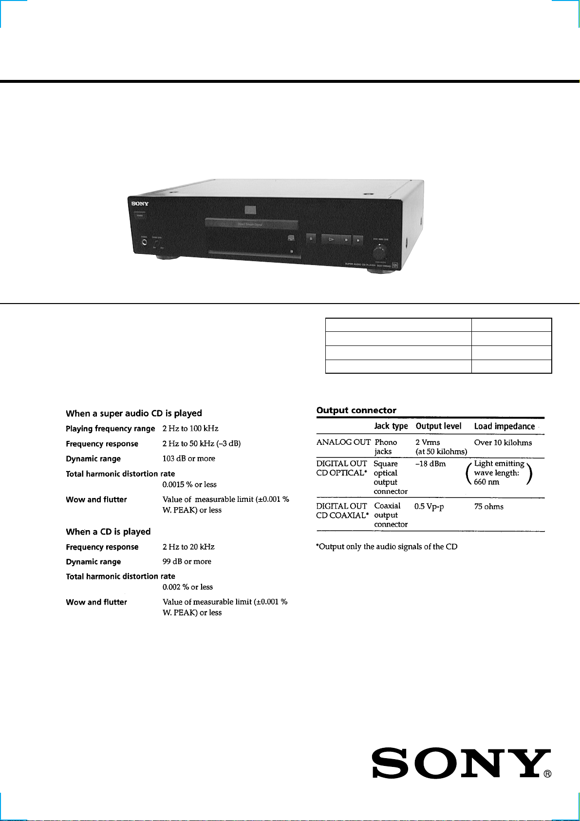
SCD-XB940
SERVICE MANUAL
Photo: Black type
SPECIFICATIONS
AEP Model
UK Model
Model Name Using Similar Mechanism NEW
CD Mechanism Type CDM55B-DVBU3
Base Unit Name DVBU3
Optical Pick-up Name KHM-220AAA/J1N
– Continued on next page –
SUPER AUDIO CD PLAYER
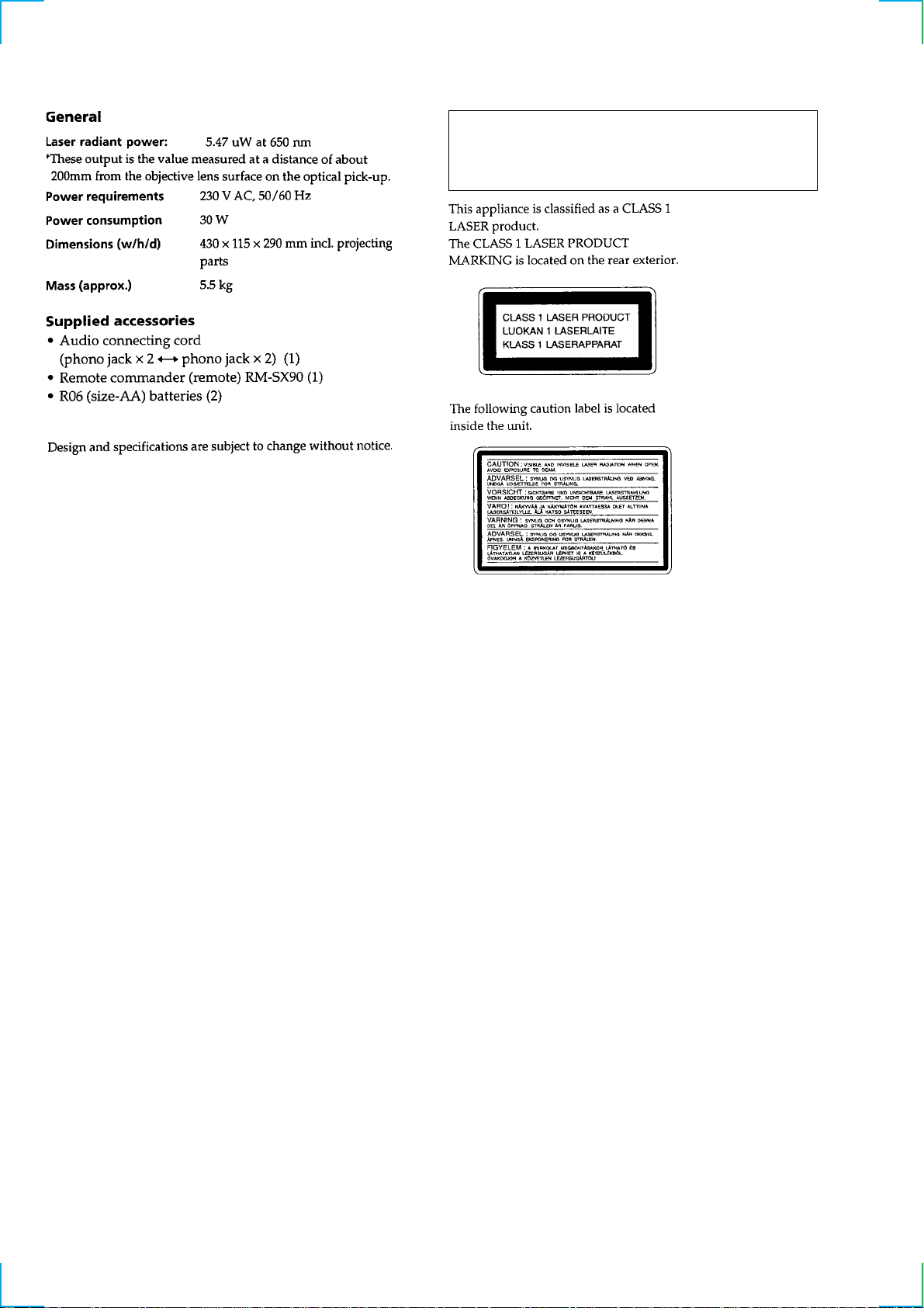
CAUTION
Use of controls or adjustments or performance of procedures
other than those specified herein may result in hazardous radiation exposure.
SAFETY-RELATED COMPONENT WARNING!!
COMPONENTS IDENTIFIED BY MARK 0 OR DOTTED
LINE WITH MARK 0 ON THE SCHEMATIC DIAGRAMS
AND IN THE PARTS LIST ARE CRITICAL TO SAFE
OPERATION. REPLACE THESE COMPONENTS WITH
SONY PARTS WHOSE PART NUMBERS APPEAR AS
SHOWN IN THIS MANUAL OR IN SUPPLEMENTS PUBLISHED BY SONY.
2
Notes on chip component replacement
• Never reuse a disconnected chip component.
• Notice that the minus side of a tantalum capacitor may be damaged by heat.
Flexible Circuit Board Repairing
• Keep the temperature of the soldering iron around 270 ˚C during repairing.
• Do not touch the soldering iron on the same conductor of the
circuit board (within 3 times).
• Be careful not to apply force on the conductor when soldering
or unsoldering.

TABLE OF CONTENTS
1. SERVICING NOTES ............................................... 4
2. GENERAL ................................................................... 5
3. DISASSEMBLY ......................................................... 8
4. DIAGRAMS
4-1. Notes for Printed Wiring Board and
Schematic Diagram ......................................................... 11
4-2. Printed Wiring Board – TK Board –.............................. 12
4-3. Schematic Diagram – TK Board – ................................ 13
4-4. Printed Wiring Board
– MAIN Board (Component Side) – .............................. 14
4-5. Printed Wiring Board
– MAIN Board (Conductor Side) – ................................ 15
4-6. Schematic Diagram – MAIN Board (1/6) – .................. 16
4-7. Schematic Diagram – MAIN Board (2/6) – .................. 17
4-8. Schematic Diagram – MAIN Board (3/6) – .................. 18
4-9. Schematic Diagram – MAIN Board (4/6) – .................. 19
4-10. Schematic Diagram – MAIN Board (5/6) – .................. 20
4-11. Schematic Diagram – MAIN Board (6/6) – .................. 21
4-12. Printed Wiring Board – AUDIO Board – ...................... 22
4-13. Schematic Diagram – AUDIO Board – ......................... 23
4-14. Printed Wiring Board – HP Board – .............................. 24
4-15. Schematic Diagram – HP Board –................................. 24
4-16. Printed Wiring Board – LOADING Board –................. 25
4-17. Schematic Diagram – LOADING Board – ................... 25
4-18. Printed Wiring Board – DISPLAY Board – .................. 26
4-19. Schematic Diagram – DISPLAY Board – ..................... 27
4-20. Printed Wiring Board – POWER Board –..................... 28
4-21. Schematic Diagram – POWER Board –........................ 29
4-22. Printed Wiring Boards
– AC SW/TRANSFORMER Boards – ........................... 30
4-23. Schematic Diagram
– AC SW/TRANSFORMER Boards – ........................... 31
5. EXPLODED VIEWS ................................................ 36
6. ELECTRICAL PARTS LIST ............................... 40
3
SECTION 1
(
SERVICING NOTES
NOTES ON HANDLING THE OPTICAL PICK-UP
BLOCK OR BASE UNIT
The laser diode in the optical pick-up block may suffer electrostatic break-down because of the potential difference generated
by the charged electrostatic load, etc. on clothing and the human
body.
During repair, pay attention to electrostatic break-down and also
use the procedure in the printed matter which is included in the
repair parts.
The flexible board is easily damaged and should be handled with
care.
NOTES ON LASER DIODE EMISSION CHECK
The laser beam on this model is concentrated so as to be focused
on the disc reflective surface by the objective lens in the optical
pick-up block. Therefore, when checking the laser diode emission, observe from more than 30 cm away from the objectiv e lens.
MODEL IDENTIFICATION
– Back Panel –
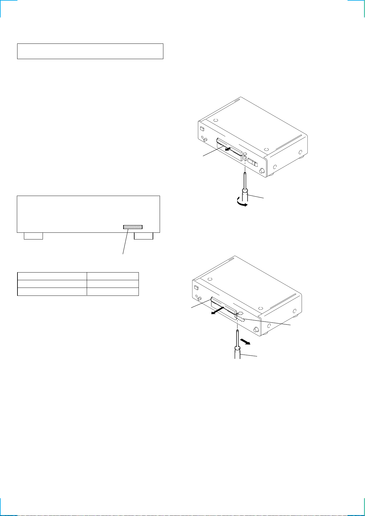
HOW TO OPEN THE TRAY WHEN POWER SWITCH
TURNS OFF
There are two different methods to open the tray.
• Method-1
Insert a screw driver (3) into the aperture of the unit bottom, and
turn it in the direction of the arrow (to OUT direction).
tray
screw driver (3)
*To close the disc table, turn the screw driver (3)
in the reverse direction
to IN direction).
Par t No.
Model Part No.
AEP 4-227-711-0
UK 4-227-711-1
• Method-2
s
s
tray
B
cam (CDM55)
A
screw driver (3)
1 Insert a screw driver (3) into the aperture of the unit bottom,
and move the cam (CDM55) in the direction of arrow A.
2 Pull the tray in the direction of arrow B.
4
SECTION 2
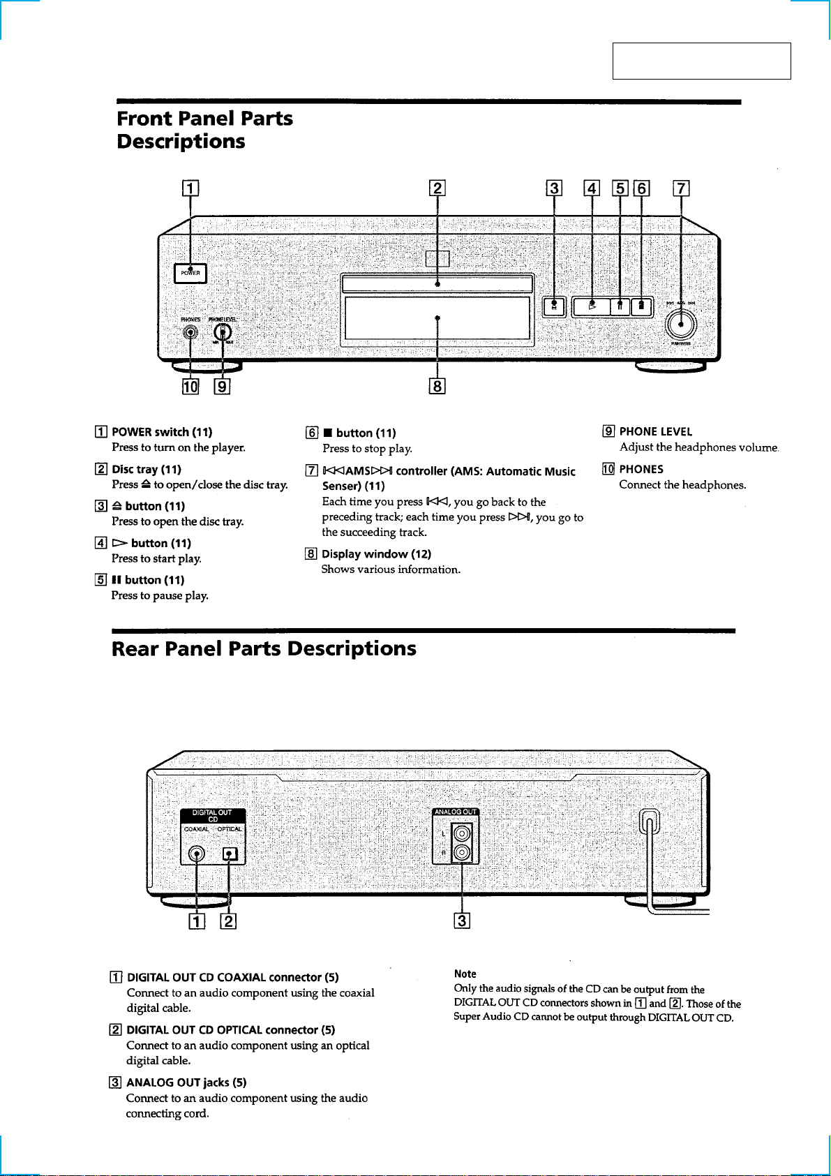
GENERAL
This section is extracted from
instruction manual.
5
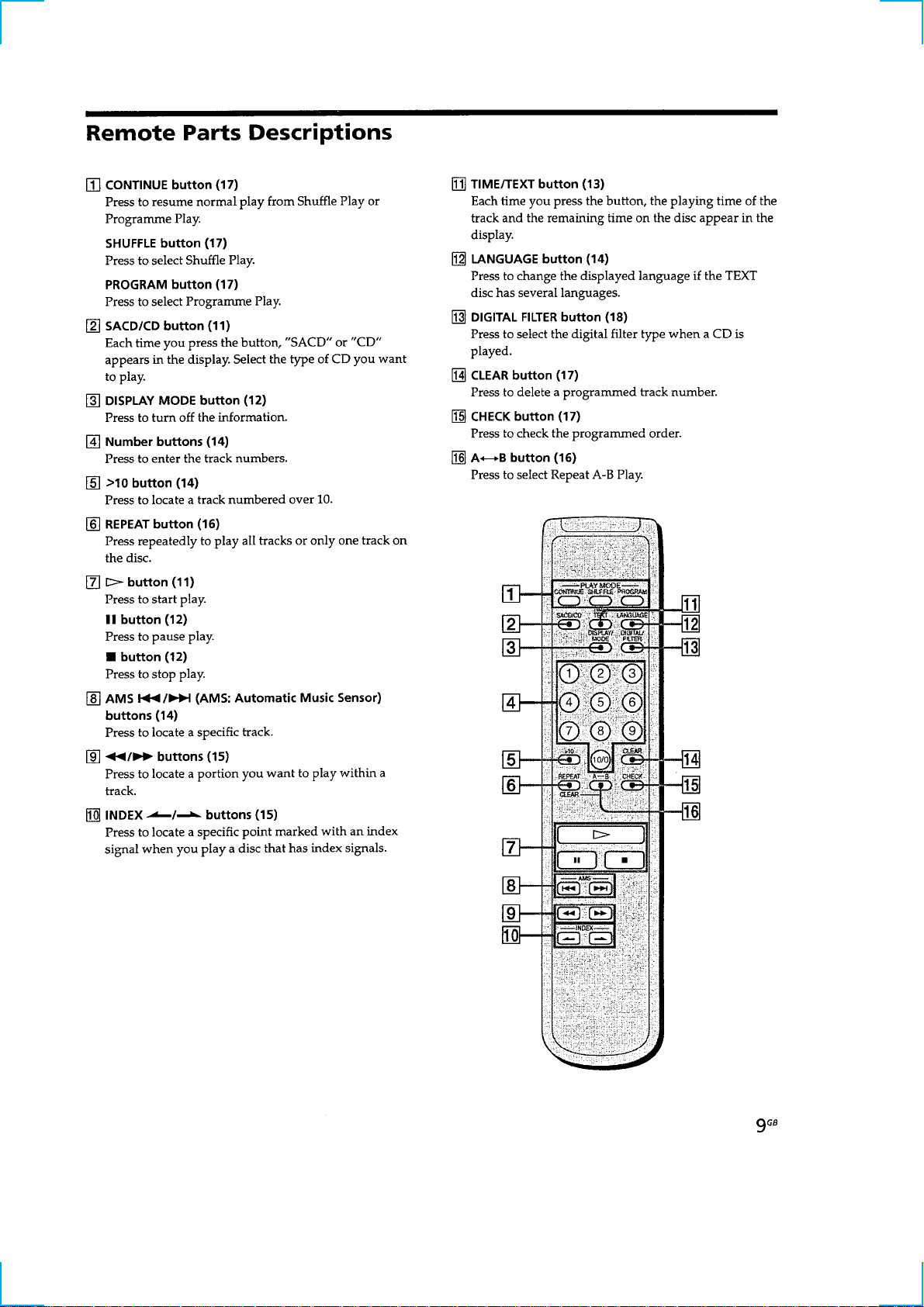
678
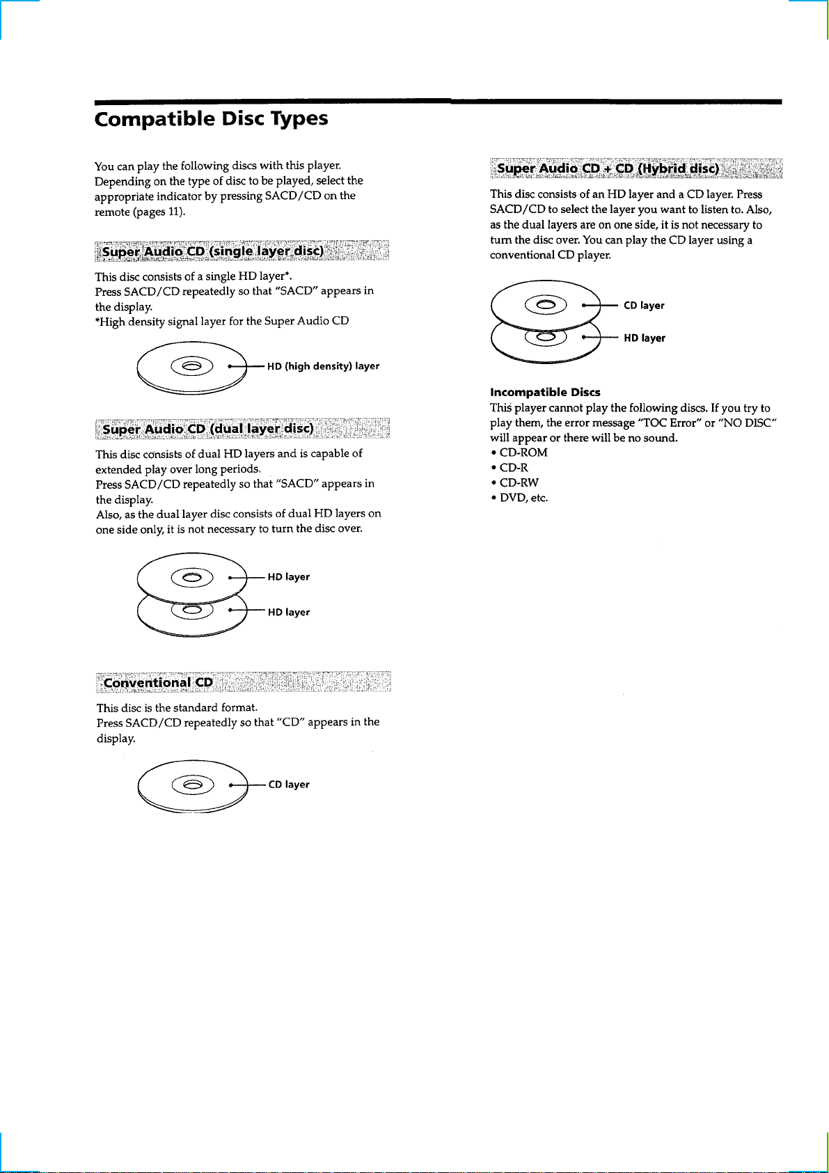
)
SECTION 3
)
DISASSEMBLY
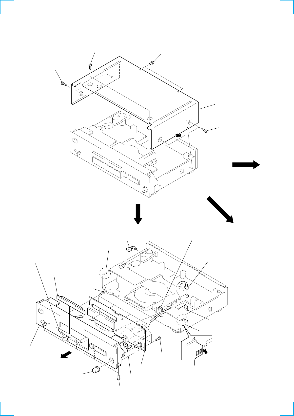
Note: Follow the disassembly procedure in the numerical order given.
COVER (4095269)
1 two screws
1 two screws
2
1 two screws
2
3 cover (4095269
1 two screws
FRONT PANEL SECTION
1 Pull out the tray.
(Refer to page 4, “HOW TO OPEN THE
TRAY WHEN POWER SWITCH TRANS OFF”.)
2 loading panel ass’y
q; five screws
(BVTP2.6 × 8)
qd front panel section
8
9 knob (AMS)
4 connector
7 two claws
6 seven screws
(BV/RING)
(CN992)
qa connector
q; eight screws
(BVTP2.6 × 8)
qs DISPLAY board
(CN201)
5 holder
7 two claws
4 connector
(CN351)
3 wire (flat type) (10 core
(CN601)
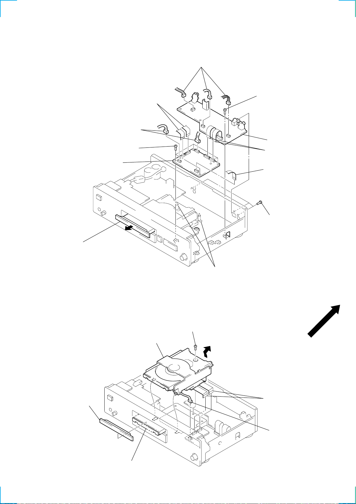
AUDIO/MAIN BOARD
6 three connectors
(CN301, 304, 351)
2 two wires (flat type) (18 core)
(CN602, 603)
3 two connectors
(CN605, 610)
4 five screws
(BVTT3 × 8)
5 MAIN board
1 Pull out the tray.
(Refer to page 4, “HO W TO OPEN THE
TRAY WHEN POWER SWITCH TRANS OFF”.)
8 screw
(BVTT3 × 8)
q; AUDIO board
2 two wires (flat type) (16 core)
(CN608, 611)
2 wire (flat type) (10 core)
(CN601)
7 three screws
(BV/RING)
MECHANISM DECK (CDM55B-DVBU3)
6 mechanism deck
(CDM55B-DVBU3)
2 loading panel ass’y
9 two PC board holders
5 screw
(BVTT3 × 8)
3 two wires (flat type) (18 core)
(CN602, 603)
4 connector
(CN605)
1 Pull out the tray.
(Refer to page 4, “HO W TO OPEN THE
TRAY WHEN POWER SWITCH TRANS OFF”.)
9
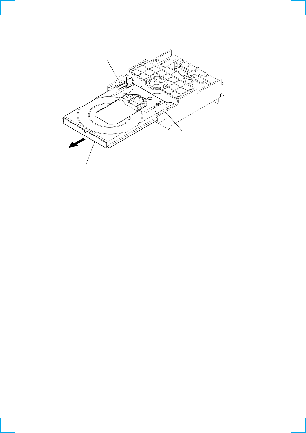
TRAY
claw
claw
1 Remove the tray. (Careful of the claw.)
10
SECTION 4
d
DIAGRAMS
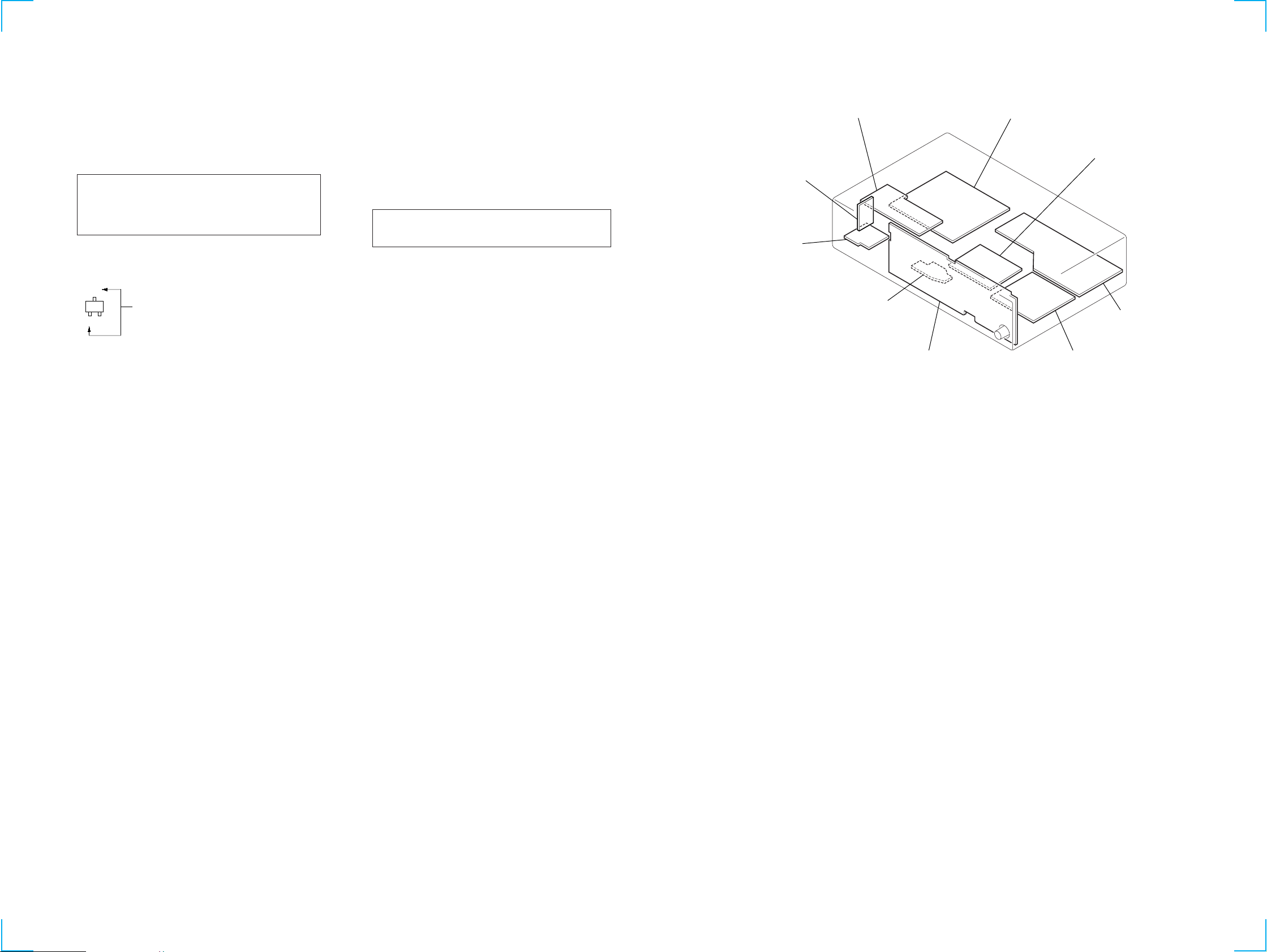
4-1. NOTE FOR PRINTED WIRING BOARDS AND SCHEMATIC DIAGRAMS
Note on Printed Wiring Board:
• X : parts extracted from the component side.
• Y : parts extracted from the conductor side.
a
•
• b : Pattern from the side which enables seeing.
(The other layers' patterns are not indicated.)
Caution:
Pattern face side: Parts on the pattern face side seen from
(Conductor Side) the pattern face are indicated.
Parts face side: Parts on the parts face side seen from
(Component Side) the parts face are indicated.
• Main board is multi-layer printed board.
• Indication of transistor
: Through hole.
However, the patterns of intermediate-layer hav e not been included in the diagram.
C
Q
B
E
These are omitted.
Note on Schematic Diagram:
• All capacitors are in µF unless otherwise noted. pF: µµF
50 WV or less are not indicated except for electrolytics
and tantalums.
• All resistors are in Ω and 1/
specified.
f
•
• 5 : fusible resistor.
• C : panel designation.
Note: The components identified by mark 0 or dotted line
• U : B+ Line.
• V : B– Line.
• Voltages and waveforms are dc with respect to ground
• V oltages are taken with a VOM (Input impedance 10 MΩ).
• Waveforms are taken with a oscilloscope.
• Circled numbers refer to waveforms.
• Signal path.
: internal component.
with mark 0 are critical for safety.
Replace only with part number specified.
under no-signal conditions.
no mark : STOP
Voltage var iations may be noted due to normal production tolerances.
Voltage var iations may be noted due to normal production tolerances.
J : SACD
c : CD
I : DIGITAL OUT
4
W or less unless otherwise
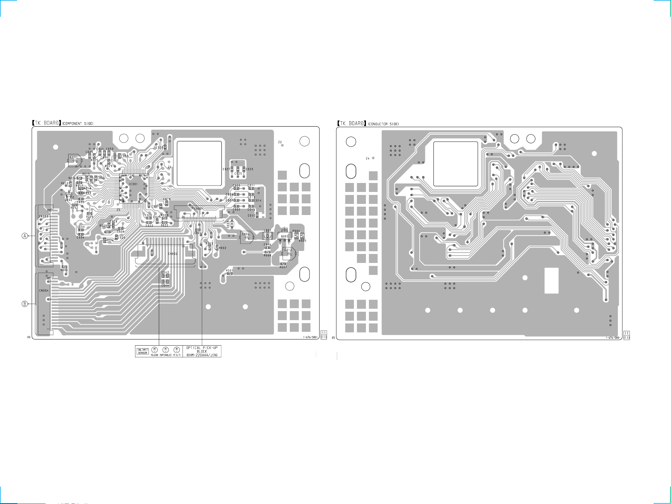
• Circuit Boards Location
AC SW board
HP board
TRANSFORMER board
LOADING board
DISPLAY board
POWER board
TK board
AUDIO boar
MAIN board
1111
SCD-XB940
4-2. PRINTED WIRING BOARD – TK Board – • See page 11 for Circuit Boards Location.
(Page 14)
(Page 14)
1212
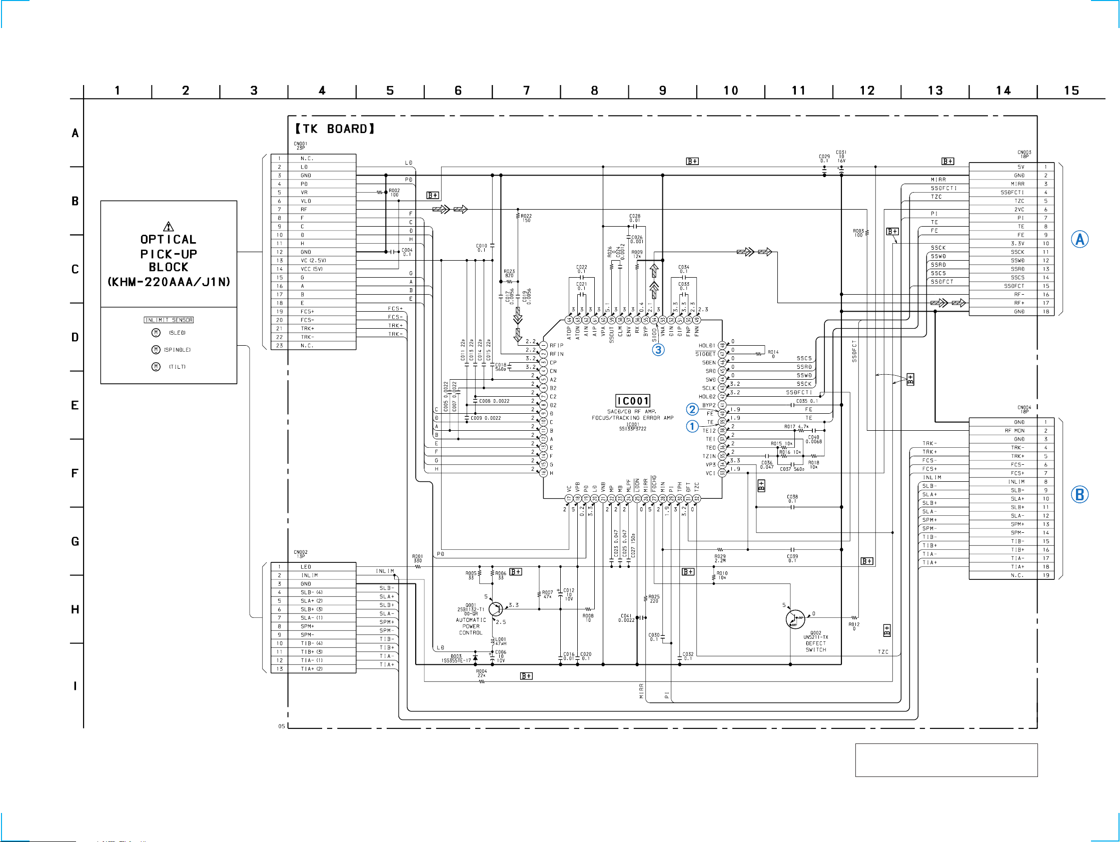
4-3. SCHEMATIC DIAGRAM – TK Board – • See page 32 for Waveforms.
SCD-XB940
(Page 16)
The components identified by mark 0 or dotted
line with mark 0 are critical for safety.
Replace only with part number specified.
(Page 16)
1313
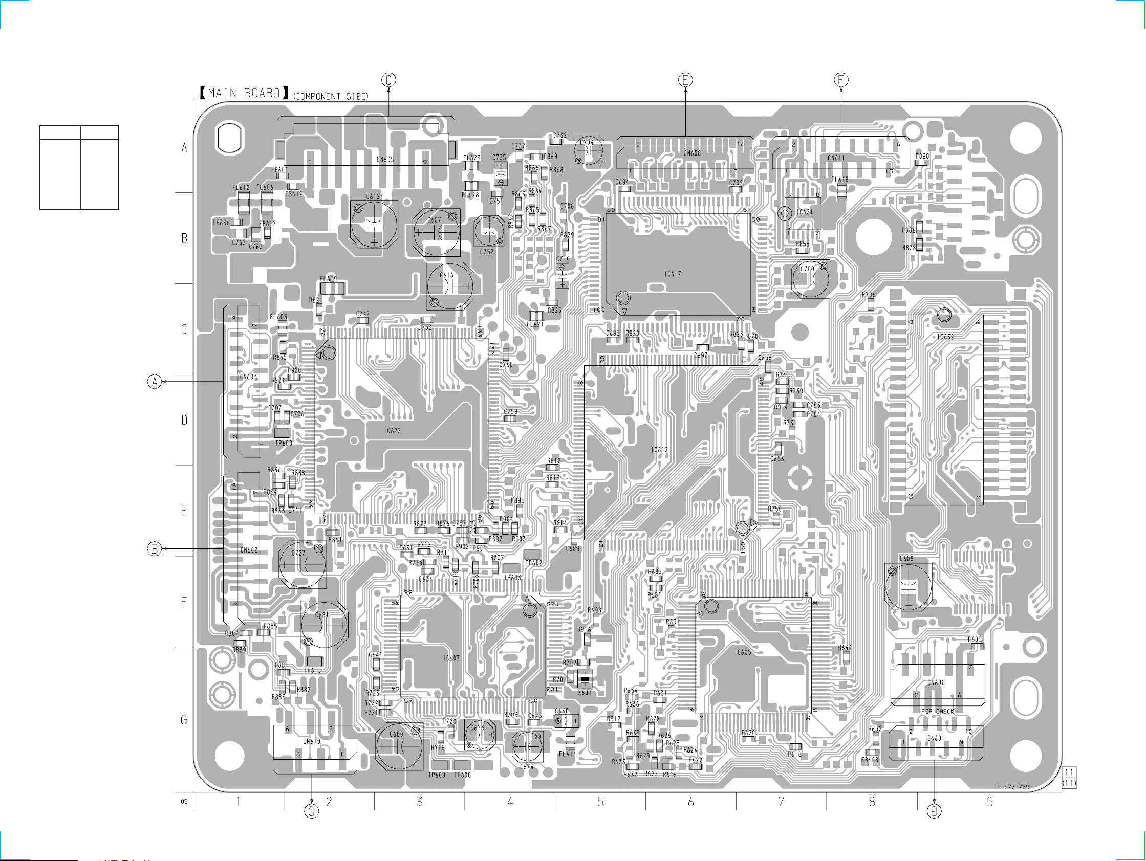
SCD-XB940
• Semiconductor
Location
Ref. No. Location
IC605 G-7
IC607 F-4
IC612 D-6
IC617 B-6
IC621 B-7
IC622 D-3
IC632 D-9
4-4. PRINTED WIRING BOARD – MAIN Board (Component Side) – • See page 11 for Circuit Boards Location.
(Page 28)
(Page 22) (Page 22)
(Page 12)
(Page 12)
(Page 25)
(Page 26)
1414
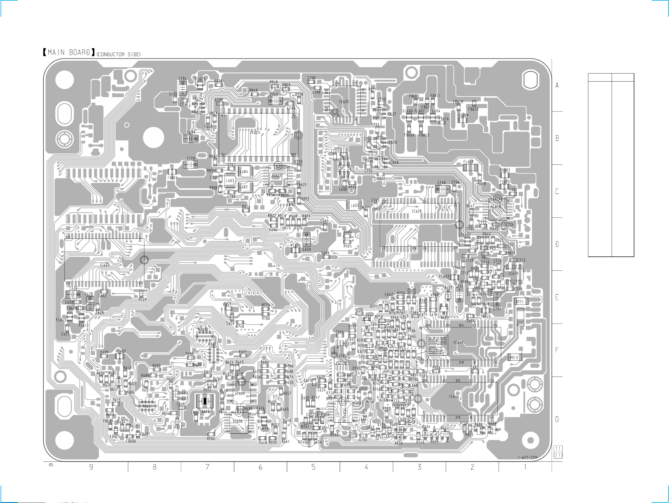
4-5. PRINTED WIRING BOARD – MAIN Board (Conductor Side) – • See page 11 for Circuit Boards Location.
SCD-XB940
• Semiconductor
Location
Ref. No. Location
D600 G-3
D604 G-3
D605 E-3
D606 G-2
D607 E-2
D608 G-2
D609 G-3
D610 G-3
D612 G-9
IC600 G-6
IC606 G-6
IC609 D-9
IC610 F-4
IC613 G-4
IC614 F-2
IC615 G-2
IC616 C-2
IC618 C-4
IC619 E-1
IC620 A-4
IC623 C-6
IC624 A-7
IC625 B-6
IC627 B-4
IC628 D-3
IC629 B-4
IC630 B-4
Q601 G-3
Q602 E-4
Q603 F-4
1515
 Loading...