

Sony SAWMSP-85 Service manual
SA-WMSP75/WMSP85
SERVICE MANUAL
Ver 1.4 2004.01
• SA-WMSP75/WMSP85 are the sub woofer
section HT-DDW750,HT-1800DP,HT-6600DP
and HT-1750DP.
POWER OUTPUT AND TOTAL
HARMONIC DISTORTION:
With 6 ohm loads, from 28 – 200 Hz; rated 75
watts (SA-WMSP75) / 100 watts (SA-WMSP85),
minimum RMS power, with no more than 0.8%
total harmonic distortion from 250 milliwatts to
rated output (Models of area code U only).
Speaker system Active subwoofer,
Speaker unit Woofer: 20 cm cone type
Enclosure type Acoustically loaded bass
Continuous RMS power output
(6 ohms, 20 – 250 Hz)
SA-WMSP75 75 W
SA-WMSP85 100 W
Reproduction frequency range
High frequency cut-off frequency
Input LINE IN (input pin jacks)
magnetically shielded
reflex
28Hz – 200 Hz
150 Hz
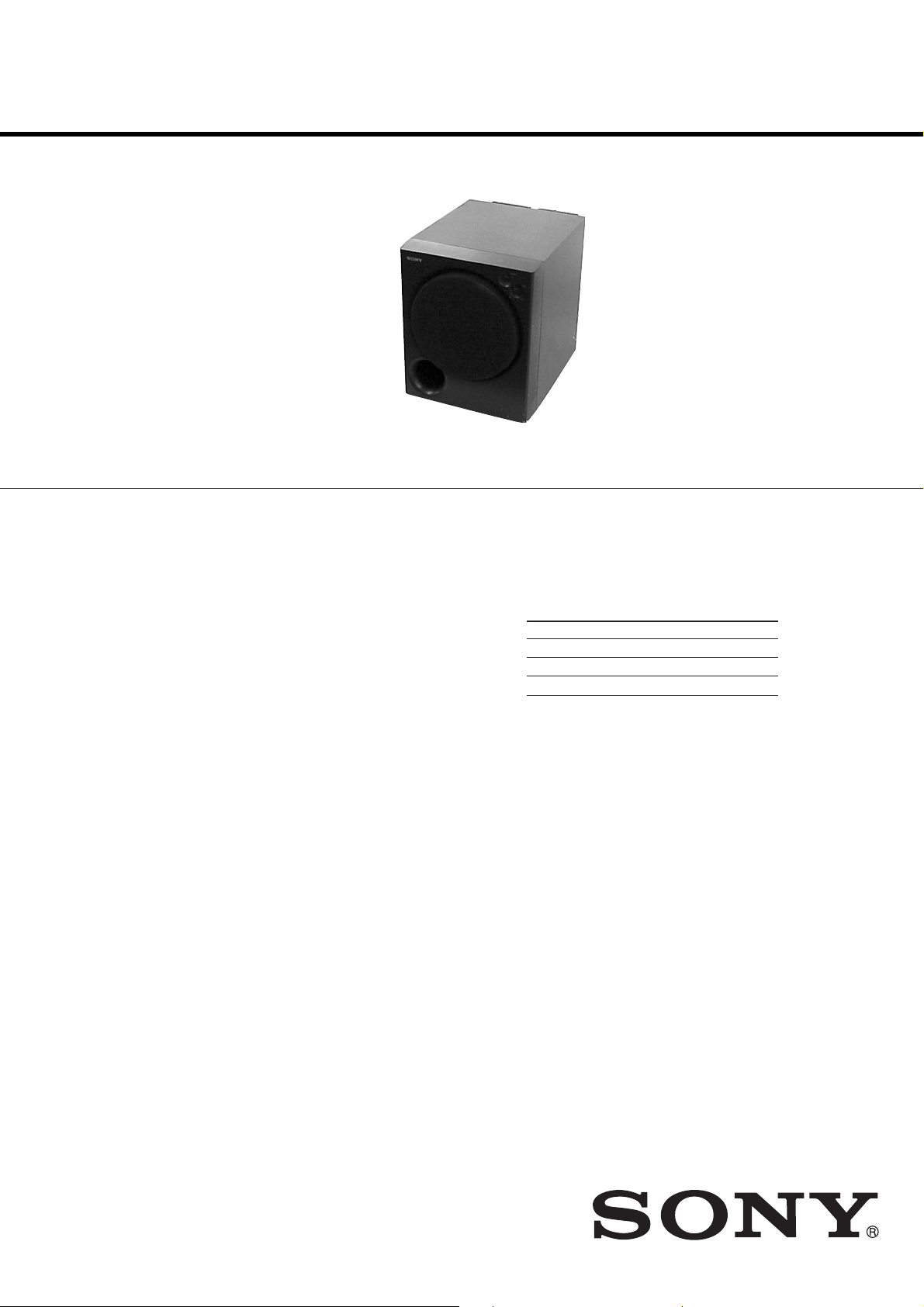
photo: SA-WMSP75
SPECIFICATION
Canadian Model
SA-WMSP75/WMSP85
AEP Model
Australian Model
Power requirements
Area code Power requirements
U, CA, MX 120 V AC, 60 Hz
CEL, CEK, SP, AU 230 V AC, 50/60 Hz
E2 120/220/230 V AC, 50/60 Hz
Power consumption
SA-WMSP75 75 W
SA-WMSP85 100 W
Dimensions (w/h/d) Approx. 270 × 325 × 398
Mass
SA-WMSP85 10.0 kg (22 lb 1 oz)
SA-WMSP75 9.0 kg (19 lb 14 oz)
•Abbreviation
AU : Australian model
CA : Canadian model
CEK : UK model
CEL : AEP model
MX : Mexican model
SP : Singapore model
U: US model
mm (10 3/4 × 12 7/8 × 15 3/4
inches) including front
panel
US Model
UK Model
E Model
SA-WMSP85
9-877-044-05
2004A16-1
© 2004.01
ACTIVE SUBWOOFER
Sony Corporation
Home Audio Company
Published by Sony Engineering Corporation

SA-WMSP75/WMSP85
SAFETY CHECK-OUT
After correcting the original service problem, perform the
following safety checks before releasing the set to the customer:
Check the antenna terminals, metal trim, “metallized” knobs, screws,
and all other exposed metal parts for AC leakage. Check leakage as
described below.
Unleaded solder
Boards requiring use of unleaded solder are printed with the leadfree mark (LF) indicating the solder contains no lead.
(Caution: Some printed circuit boards may not come printed with
the lead free mark due to their particular size.)
LEAKAGE
The AC leakage from any exposed metal part to earth ground and
from all exposed metal parts to any exposed metal part having a
return to chassis, must not exceed 0.5 mA (500 microamperes).
Leakage current can be measured by any one of three methods.
1. A commercial leakage tester, such as the Simpson 229 or RCA
WT -540A. Follo w the manufacturers’ instructions to use these
instruments.
2. A battery-operated AC milliammeter. The Data Precision 245
digital multimeter is suitable for this job.
3. Measuring the voltage drop across a resistor by means of a
VOM or battery-operated AC v oltmeter. The “limit” indication
is 0.75 V, so analog meters must have an accurate low-v oltage
scale. The Simpson 250 and Sanwa SH-63Trd are e xamples of
a passive VOM that is suitable. Nearly all battery operated
digital multimeters that have a 2V AC range are suitable. (See
Fig. A)
To Exposed Metal
Parts on Set
: LEAD FREE MARK
Unleaded solder has the following characteristics.
• Unleaded solder melts at a temperature about 40°C higher than
ordinary solder.
Ordinary soldering irons can be used but the iron tip has to be
applied to the solder joint for a slightly longer time.
Soldering irons using a temperature regulator should be set to
about 350°C.
Caution: The printed pattern (copper foil) may peel away if the
heated tip is applied for too long, so be careful!
• Strong viscosity
Unleaded solder is more viscous (sticky , less prone to flow) than
ordinary solder so use caution not to let solder bridges occur such
as on IC pins, etc.
• Usable with ordinary solder
It is best to use only unleaded solder but unleaded solder may
also be added to ordinary solder.
0.15µF
Ω
1.5k
Earth Ground
AC
voltmeter
(0.75V)
Fig. A. Using an AC voltmeter to check AC leakage.
SAFETY-RELATED COMPONENT WARNING!!
COMPONENTS IDENTIFIED BY MARK 0 OR DOTTED LINE WITH
MARK 0 ON THE SCHEMATIC DIAGRAMS AND IN THE PARTS
LIST ARE CRITICAL TO SAFE OPERATION. REPLACE THESE
COMPONENTS WITH SONY PARTS WHOSE PART NUMBERS
APPEAR AS SHOWN IN THIS MANUAL OR IN SUPPLEMENTS
PUBLISHED BY SONY .
ATTENTION AU COMPOSANT AYANT RAPPORT
À LA SÉCURITÉ!
LES COMPOSANTS IDENTIFÉS P AR UNE MARQUE 0 SUR LES
DIAGRAMMES SCHÉMA TIQUES ET LA LISTE DES PIÈCES SONT
CRITIQUES POUR LA SÉCURITÉ DE FONCTIONNEMENT. NE
REMPLACER CES COMPOSANTS QUE PAR DES PIÈSES SONY
DONT LES NUMÉROS SONT DONNÉS DANS CE MANUEL OU
DANS LES SUPPÉMENTS PUBLIÉS PAR SONY.
2
SA-WMSP75/WMSP85
D
1 2 3 4 5 6 7 8 9 10 11 12
SUB
SECTION 1
DIAGRAMS
THIS NOTE IS COMMON FOR PRINTED WIRING BOARDS AND SCHEMATIC DIAGRAMS.
(In addition to this, the necessary note is printed in each bloc k.)
Note on Printed Wiring Boards:
• X : parts extracted from the component side.
• Y : parts extracted from the conductor side.
• b : Pattern from the side which enables seeing.
Note on Schematic Diagram:
• All capacitors are in µF unless otherwise noted. p: pF. 50
WV or less are not indicated except for electrolytics and
tantalums.
• 2 : nonflammable resistor.
• 5 : fusible resistor.
• All resistors are in Ω and 1/
specified.
• C : panel designation.
The components identified by
mark 0 or dotted line with mark
0 are critical for safety.
Replace only with part number
specified.
• A : B+ Line.
• B : B– Line.
•Voltages are dc with respect to ground under no-signal
conditions.
no mark : Power on
•Voltages are taken with a VOM (Input impedance 10MΩ).
Voltage v ariations may be noted due to normal preduction
tolerances.
• Signal path.
F : AUDIO
•Abbreviation
CND : Canadian model.
E2 : 120V AC Area in E model.
MX : Mexican model.
4
W or less unless otherwise
Les composants identifiés par
une marque 0 sont critiques
pour la sécurité.
Ne les remplacer que par une
pièce portant le numéro spécifié.
1-2. IC Block Diagrams
IC301 STK404-130S (MAIN Board)
2 31 4 5 6 7 8 9 10 11 12 13
SUB
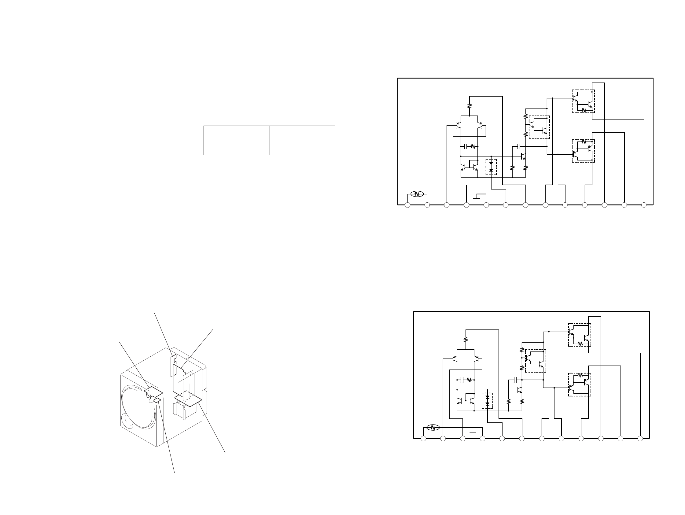
1-1. Circuit Board Location
SWITCH BOARD
IC301 STK-404-100S (MAIN Board)
INPUT(CONTROL) BOARD
MAIN BOARD
POWER TRANS BOAR
CONTROL BOARD
33
SA-WMSP75/WMSP85
Ver 1.2 2003.06
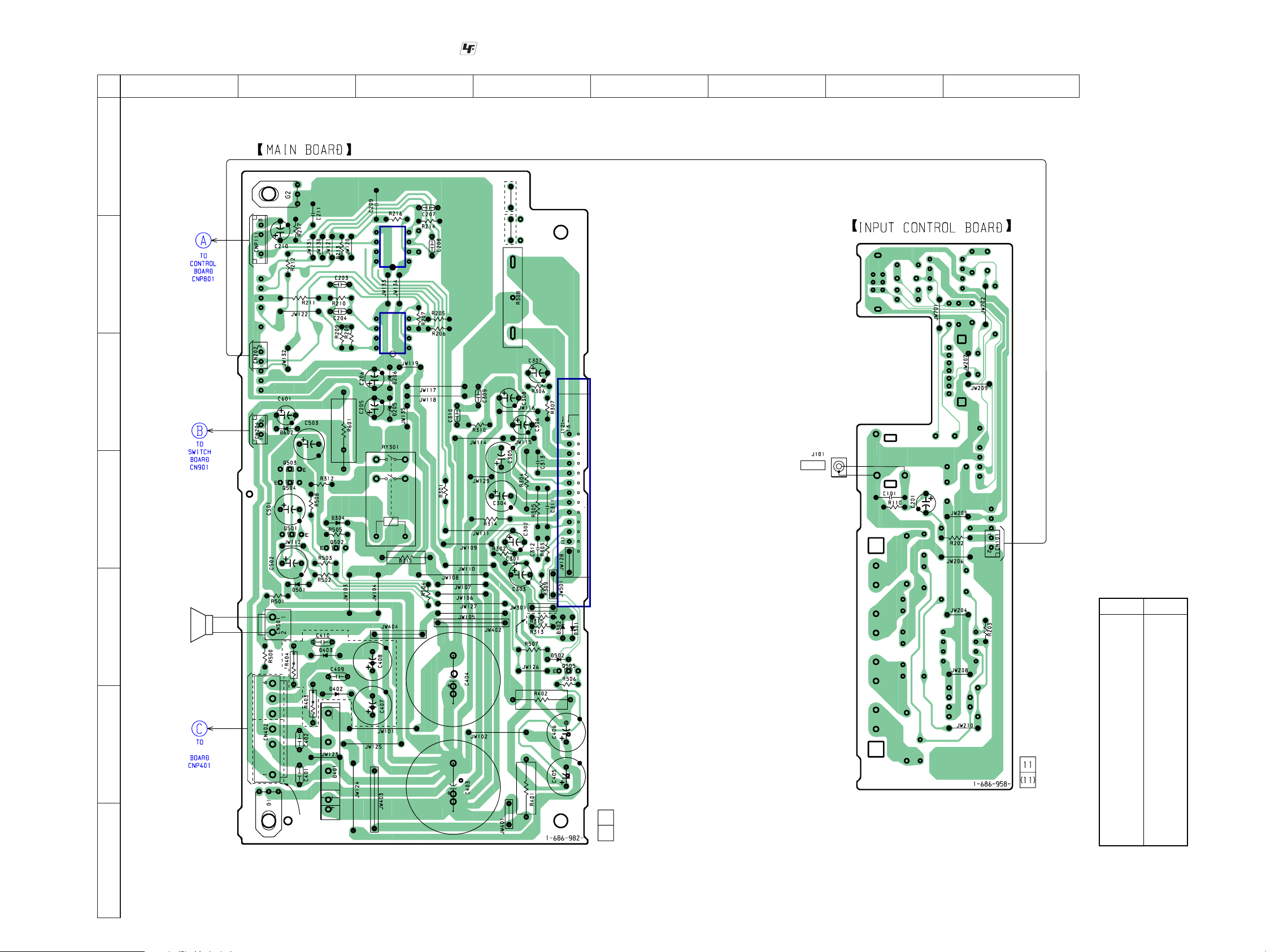
1-3. Printed Wiring Board – MAIN Section –
• See page 3 for Circuit Boards Location.
•
: Uses unleaded solder.
A
B
C
12
4
IC203
1
4
IC202
1
345678
WMSP75
5
WMSP85
8
5
8
WMSP75
WMSP85
()
D
E
F
SP1
POWER TRANS
WMSP85
WMSP75
INPUT
IC301
• Semiconductor
Location
Ref. No. Location
D205 C-3
D206 C-3
D301 E-4
D302 E-4
D304 D-2
D401 F-2
D402 F-2
D403 E-2
D501 E-2
D502 E-4
D602 C-2
IC202 B-3
IC203 B-3
IC301 D-4
G
CN402
WMSP75 : 3P
WMSP85 : 6P
11
(11)
Q501 D-2
Q502 D-2
Q503 D-2
Q504 D-2
Q505 E-4
44
 Loading...