

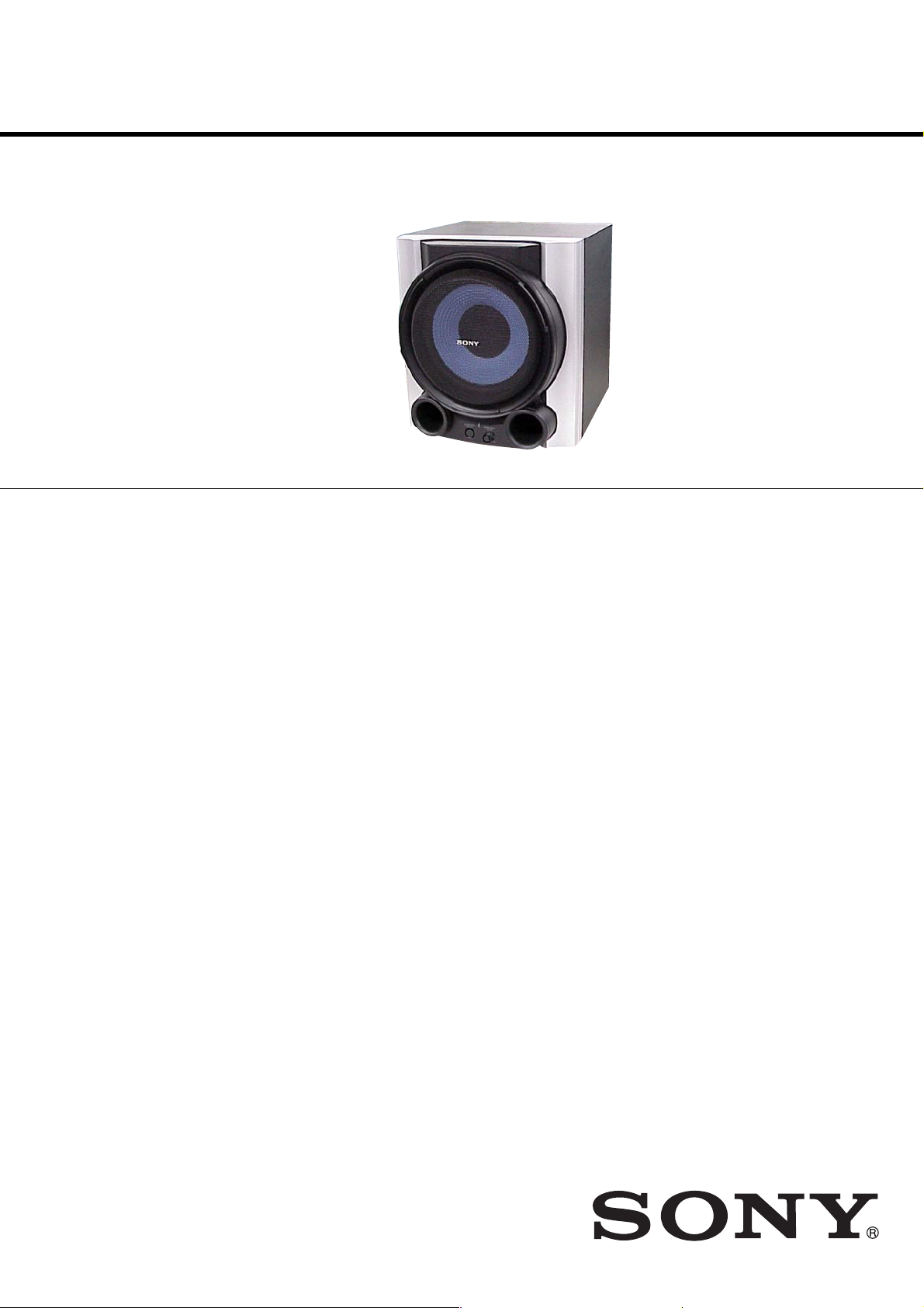
SA-WG99
SERVICE MANUAL
Ver. 1.0 2007.01
• SA-WG99 is the sub woofer section
in MHC-GX99.
SPECIFICATIONS
Speaker system: bass-reflex type
Speaker units
Woofer: 20 cm, cone type
Nominal impedance: 6 Ω
Power requirement:
North American model: AC 120 V, 60 Hz
Power consumption:
US model: 115 W
Canadian model: 155 VA
Dimensions (w/h/d): Approx. 280 × 306 × 405 mm
Mass: Approx. 8.7 kg
US Model
Canadian Model
Design and specifications are subject to change without notice.
ACTIVE SUBWOOFER
9-887-535-01
2007A16-1
© 2007.01
Sony Corporation
Home Audio Division
Published by Sony Techno Create Corporation
SA-WG99
r
SAFETY CHECK-OUT
After correcting the original service problem, perform the following
safety check before releasing the set to the customer:
Check the antenna terminals, metal trim, “metallized” knobs, screws,
and all other exposed metal parts for AC leakage.
Check leakage as described below.
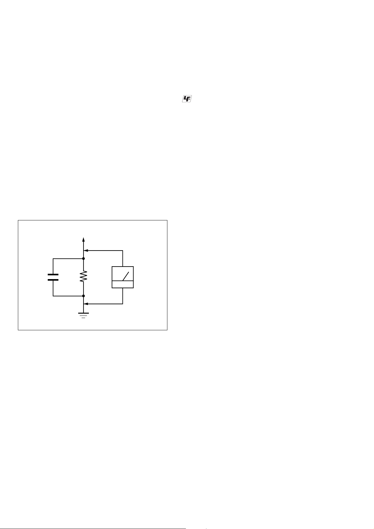
LEAKAGE TEST
The AC leakage from any exposed metal part to earth ground and
from all exposed metal parts to any exposed metal part having a
return to chassis, must not exceed 0.5 mA (500 microamperes.).
Leakage current can be measured by any one of three methods.
1. A commercial leakage tester, such as the Simpson 229 or RCA
WT -540A. Follow the manuf acturers’ instructions to use these
instruments.
2. A battery-operated A C milliammeter . The Data Precision 245
digital multimeter is suitable for this job.
3. Measuring the voltage drop across a resistor by means of a
VOM or battery-operated AC v oltmeter. The “limit” indication
is 0.75 V, so analog meters must hav e an accurate low-v oltage
scale. The Simpson 250 and Sanwa SH-63Trd are examples
of a passive VOM that is suitable. Nearly all battery operated
digital multimeters that have a 2 V AC range are suitable. (See
Fig. A)
To Exposed Metal
Parts on Set
UNLEADED SOLDER
Boards requiring use of unleaded solder are printed with the leadfree mark (LF) indicating the solder contains no lead.
(Caution: Some printed circuit boards may not come printed with
the lead free mark due to their particular size)
: LEAD FREE MARK
Unleaded solder has the following characteristics.
• Unleaded solder melts at a temperature about 40 °C higher
than ordinary solder.
Ordinary soldering irons can be used but the iron tip has to be
applied to the solder joint for a slightly longer time.
Soldering irons using a temperature regulator should be set to
about 350 °C.
Caution: The printed pattern (copper foil) may peel away if
the heated tip is applied for too long, so be careful!
• Strong viscosity
Unleaded solder is more viscou-s (sticky, less prone to flow)
than ordinary solder so use caution not to let solder bridges
occur such as on IC pins, etc.
• Usable with ordinary solder
It is best to use only unleaded solder but unleaded solder may
also be added to ordinary solder.
AC
0.15 µF
1.5 k
Ω
Earth Ground
voltmete
(0.75 V)
Fig. A. Using an AC voltmeter to check AC leakage.
SAFETY-RELATED COMPONENT WARNING!!
COMPONENTS IDENTIFIED BY MARK 0 OR DOTTED LINE
WITH MARK 0 ON THE SCHEMATIC DIAGRAMS AND IN
THE PARTS LIST ARE CRITICAL TO SAFE OPERATION.
REPLACE THESE COMPONENTS WITH SONY PARTS WHOSE
PART NUMBERS APPEAR AS SHOWN IN THIS MANUAL OR
IN SUPPLEMENTS PUBLISHED BY SONY.
ATTENTION AU COMPOSANT AYANT RAPPORT
À LA SÉCURITÉ!
LES COMPOSANTS IDENTIFIÉS PAR UNE MARQUE 0 SUR
LES DIAGRAMMES SCHÉMATIQUES ET LA LISTE DES
PIÈCES SONT CRITIQUES POUR LA SÉCURITÉ DE
FONCTIONNEMENT. NE REMPLACER CES COM- POSANTS
QUE PAR DES PIÈCES SONY DONT LES NUMÉROS SONT
DONNÉS DANS CE MANUEL OU D ANS LES SUPPLÉMENTS
PUBLIÉS PAR SONY.
2
SECTION 1
DIAGRAMS
THIS NOTE IS COMMON FOR PRINTED WIRING BOARDS AND SCHEMATIC DIAGRAMS.
(In addition to this, the necessary note is printed in each block.)
Note on Printed Wiring Boards:
• X : Parts extracted from the component side.
• a : Through hole.
• : Pattern from the side which enables seeing.
Note on Schematic Diagrams:
• All capacitors are in µF unless otherwise noted. (p: pF) 50
WV or less are not indicated except for electrolytics and
tantalums.
• 2 : nonflammable resistor.
• 5 : fusible resistor.
• All resistors are in Ω and 1/
specified.
• C : panel designation.
Note:
The components identified by mark 0 or dotted line with mark 0 are
critical for safety.
Replace only with part
number specified.
• A : B+ Line.
• B : B– Line.
•Voltages and dc with respect to ground under no-signal
conditions.
no mark : Power on
•Voltages are taken with a VOM (Input impedance 10 MΩ).
Voltage variations may be noted due to normal production
tolerances.
• Signal path.
d : AUDIO
4
W or less unless otherwise
Note:
Les composants identifiés
par une marque 0 sont critiques pour la sécurité.
Ne les remplacer que par une
piéce portant le numéro
spécifié.
SA-WG99
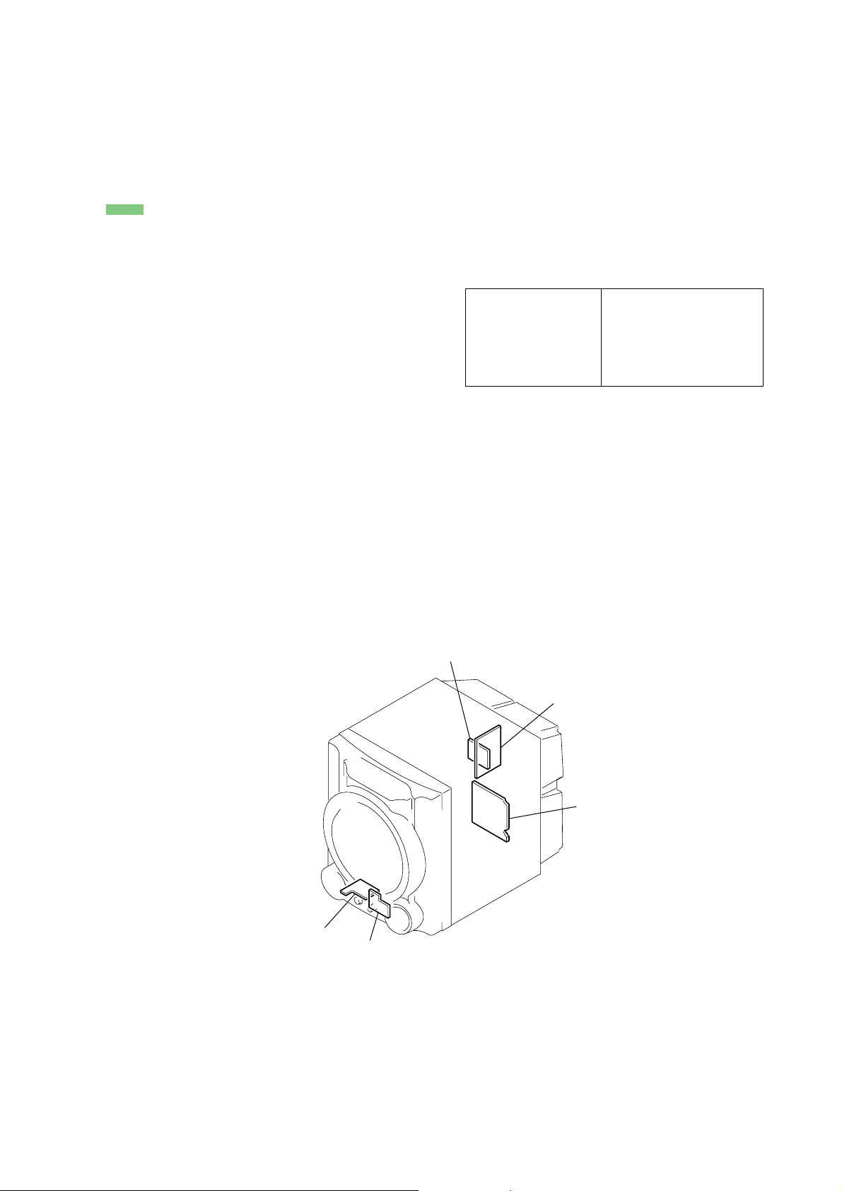
• Circuit Boards Location
POWER SWITCH board
INPUT board
POWER board
MAIN board
VOL-LED board
3

SA-WG99
• IC Block Diagram
– MAIN Board –
IC400 STK404-130S
1 2
PT-1
Power STAGE
Bias
Pre DRIVER
+
–
SUB
3
4
PT-2
SW IN
5 6 7 8 9 10 11 12 13
SUB
-PRE
SW IN NF
+PRE (12V)
-VCC
+VCC
-RE
+RE
4

SA-WG99
1-1. PRINTED WIRING BOARDS — MAIN SECTION —
2345678910111
A
INPUT BOARD
J100
INPUT
J100
B
CN100
2
1
12
1-872-050-
(12)
C
D
VOL-LED BOARD
SUBWOOFER
ON/OFF
E
D300
SUBWOOFER
LEVEL
MIN MAX
R300
F
1
CN300
5
1-872-051-
G
• :Uses unleaded solder. • See page 3 for Circuit Boards Location.
MAIN BOARD
(CHASSIS)
A001
RV300
12
(12)
FAN
R203
C205
R200
R214
R400
R201
1
3
C206
CN201
JW218
C506
C403
C401
CN501
C200
CN200
R402
R202
Q200
R209
C207
JW216
E
Q508
E
R204
R207
R206
R213
R211
Q202
R606
R205
R208
R210
E
R212
C504
E
C202
E
JW202
R518
Q507
R517
R515
C203
Q201
C204
Q506
R519
E
R605
R520
JW214
D504
R514
E
D609
D608
C607
JW212
JW207
C605
Q600
R509
R516
R504
C503
Q505
R401
D607
E
R607
C502
R534
Q504
E
D605
R511
R506
C505
R507
R512
D606
R521
JW210
Q503
R510
JW204
8
D506
1
C601
JW213
D603
JW209
R508
E
JW211
C408
C400
CN600
JW205
POWER BOARD
A
C600
D602
R602R603
C404
JW400
R414
IC400
CN702
(Page 7)
R405
R403
1
C603
R408
R418
R419
JW217
R406
R404
R416
C406
R409
R407
R417
JW201
JW206
13
D600
D601
C602
JW203
D502
C410
R410
R522
JW219
R420
R527
C409
D400
CN500
R413
Q400
ET600
R513
RY500
R505
E
R421
R411
R523
C407
R528
D509
D507
D505
JW401
R535
R412
Q511
1-872-047-
D508
C510
E
C507
R529
E
Q510
R524
Q509
JW208
R533
C509
C508
R525
R531
R526
R532
12
(12)
SPEAKER
(CHASSIS)
• Semiconductor
Location
Ref. No.
D300 E-2
D400 G-9
D502 F-9
D504 F-6
D505 D-10
D506 D-7
D507 C-10
D508 F-10
D509 C-10
D600 B-9
D601 C-9
D602 D-7
D603 D-7
D605 E-7
D606 B-7
D607 B-6
D608 B-6
D609 B-6
IC400 G-8
Q200 C-5
Q201 D-6
Q202 D-6
Q400 G-9
Q503 G-7
Q504 G-6
Q505 G-6
Q506 G-6
Q507 F-6
Q508 E-5
Q509 F-10
Q510 E-10
Q511 G-10
Q600 D-6
Location
SA-WG99
H
55
 Loading...