

Page 1

SAVA-D900/D900FR/
D900R/SS-T900
SERVICE MANUAL
(Photo : SAVA-D900FR)
(Photo : SAVA-D900)
(Photo : SS-T900)
This set is composed of the following table.
Front Speaker SAVA-D900FR
Center/Rear Speaker SS-T900
Woofer Speaker SAVA-D900R
Main Unit SAVA-D900
SPECIFICATIONS
Model Name Using Similar Mechanism NEW
Mechanism T ype CDM53J-DVBU1
Base Unit Type DVBU1
Optical Pick-up Type KHM-220AAA
US Model
(Photo : SAVA-D900R)
— Continued on next page —
DVD HOME THEATER
ACTIVE SPEAKER SYSTEM
Page 2
SAFETY CHECK-OUT
After correcting the original service problem, perform the following
safety checks before releasing the set to the customer:
Check the antenna terminals, metal trim, “metallized” knobs, screws,
and all other exposed metal parts for A C leakag e. Check leakage as
described below.
Laser component in this product is capable of emitting radiation
exceeding the limit for Class 1.
This appliance is classified as
a CLASS 1 LASER product.
The CLASS 1 LASER
PRODUCT MARKING is
located on the rear exterior.
This caution
label is located
inside the unit.
CAUTION
Use of controls or adjustments or performance of procedures
other than those specified herein may result in hazardous
radiation exposure.
Notes on chip component replacement
• Never reuse a disconnected chip component.
• Notice that the minus side of a tantalum capacitor may be
damaged by heat.
LEAKAGE
The AC leakage from any exposed metal part to earth Ground and
from all exposed metal parts to any exposed metal part having a
return to chassis, must not exceed 0.5 mA (500 microampers).
Leakage current can be measured by any one of three methods.
1. A commercial leakage tester, such as the Simpson 229 or RCA
WT -540A. Follo w the manufacturers’ instructions to use these
instruments.
2. A battery-operated AC milliammeter. The Data Precision 245
digital multimeter is suitable for this job.
3. Measuring the voltage drop across a resistor by means of a
VOM or battery-operated AC v oltmeter . The “limit” indication
is 0.75 V, so analog meters must have an accurate low-voltage
scale. The Simpson 250 and Sanwa SH-63Trd ar e examples of
a passive VOM that is suitable. Nearly all battery operated
digital multimeters that have a 2V AC range are suitable. (See
Fig. A)
To Exposed Metal
Parts on Set
0.15µF
Ω
1.5k
Earth Ground
AC
voltmeter
(0.75V)
Fig. A. Using an AC voltmeter to check AC leakage.
Flexible Circuit Board Repairing
• Keep the temperature of soldering iron around 270˚C
during repairing.
• Do not touch the soldering iron on the same conductor of the
circuit board (within 3 times).
• Be careful not to apply force on the conductor when soldering
or unsoldering.
SAFETY-RELATED COMPONENT WARNING !!
COMPONENTS IDENTIFIED BY MARK 0 OR DOTTED LINE
WITH MARK 0 ON THE SCHEMATIC DIAGRAMS AND IN
THE PARTS LIST ARE CRITICAL TO SAFE OPERATION.
REPLACE THESE COMPONENTS WITH SONY PARTS
WHOSE PART NUMBERS APPEAR AS SHOWN IN THIS
MANUAL OR IN SUPPLEMENTS PUBLISHED BY SONY.
2
Page 3

TABLE OF CONTENTS
1. GENERAL ......................................................................... 4
2. DISASSEMBLY
2-1. Grille Frame (B) Assy ................................................... 6
2-2. Amplifier Assy .............................................................. 6
2-3. Amplifier Chassis .......................................................... 7
2-4. AMP Board ................................................................... 7
2-5. Power Transformer (T900) ............................................ 8
2-6. PS Board........................................................................8
2-7. Mechanism Section .......................................................9
2-8. Video Board................................................................... 9
2-9. Main Board and DVD Board....................................... 10
2-10.Mechanism (CDM53J-DVBU1) ................................. 10
2-11.Base Unit (DVBU1) ....................................................11
2-12.Magnet Assy ................................................................ 11
2-13.Tray (SUB) .................................................................. 12
2-14.Chassis (Mold B), Stocker, Slider (Selection)............. 12
2-15.How to Assemble the Gears ........................................13
2-16.How to Attach the Slider (Selection)........................... 13
2-17.How to Attach the Stocker........................................... 14
2-18.How to Attach the Chassis (Mold B)........................... 14
3. TEST MODE.....................................................................15
4. ELECTRICAL ADJUSTMENT ................................. 26
4-1. Adjustment of Video System ....................................... 26
4-2. Adjustment Related Parts Arrangement ...................... 27
6. EXPLODED VIEWS
6-1. Overall Section ............................................................ 72
6-2. Main Unit (SAVA-D900) Section................................73
6-3. Main Chassis Section ..................................................74
6-4. Amplifier Chassis Section ........................................... 75
6-5. Mechanism Section-1 (CDM53J-DVBU1) ................. 76
6-6. Mechanism Section-2 (CDM53J-DVBU1) ................. 77
6-7. Woofer Speaker (SAVA-D900R) Section .................... 78
6-8. Front Speaker (SAVA-D900FR) Section ..................... 79
6-9. Center/Rear Speaker (SS-T900) Section ..................... 80
7. ELECTRICAL PARTS LIST.................................81
5. DIAGRAMS
5-1. Circuit Boards Location ..............................................28
5-2. Block Diagrams ........................................................... 30
– DVD Section – .........................................................30
– Main Section – ......................................................... 31
5-3. Printed Wiring Board – DVD Section – ...................... 32
5-4. Schematic Diagram – DVD (1/12) Section – .............. 34
5-5. Schematic Diagram – DVD (2/12) Section – .............. 35
5-6. Schematic Diagram – DVD (3/12) Section – .............. 36
5-7. Schematic Diagram – DVD (4/12) Section – .............. 37
5-8. Schematic Diagram – DVD (5/12) Section – .............. 38
5-9. Schematic Diagram – DVD (6/12) Section – .............. 39
5-10.Schematic Diagram – DVD (7/12) Section – .............. 40
5-11.Schematic Diagram – DVD (8/12) Section – .............. 41
5-12.Schematic Diagram – DVD (9/12) Section – .............. 42
5-13.Schematic Diagram – DVD (10/12) Section – ............ 43
5-14.Schematic Diagram – DVD (11/12) Section – ............ 44
5-15.Schematic Diagram – DVD (12/12) Section – ............ 45
5-16.Printed Wiring Board – TK Section – ......................... 46
5-17.Schematic Diagram – TK Section – ............................ 47
5-18. Schematic Diagram – MAIN Section – ...................... 48
5-19. Printed Wiring Board – MAIN Section – ................... 49
5-20. Schematic Diagram – AMP Section – ........................ 50
5-21. Printed Wiring Board – AMP Section –...................... 51
5-22. Schematic Diagram – VIDEO Section –..................... 52
5-23.Printed Wiring Board – VIDEO Section – .................. 53
5-24.Schematic Diagram – DISPLAY Section – ................. 54
5-25.Printed Wiring Board – DISPLAY Section – .............. 55
5-26.Schematic Diagram – MOTOR Section – ................... 56
5-27.Printed Wiring Board – MOTOR Section – ................ 57
5-28.Printed Wiring Board – PS Section – .......................... 58
5-29.Schematic Diagram – PS (1/2) Section – ....................60
5-30.Schematic Diagram – PS (2/2) Section – ...................61
5-31.Printed Wiring Board – POWER Section –................. 62
5-32.IC Pin Functions .......................................................... 63
5-33.IC Block Diagrams ...................................................... 67
NOTES ON HANDLING THE OPTICAL PICK-UP BLOCK
OR BASE UNIT
The laser diode in the optical pick-up block may suffer electrostatic
break-down because of the potential difference generated by the
charged electrostatic load, etc. on clothing and the human body.
During repair, pay attention to electrostatic break-down and also
use the procedure in the printed matter which is included in the
repair parts.
The flexible board is easily damaged and should be handled with
care.
NOTES ON LASER DIODE EMISSION CHECK
The laser beam on this model is concentrated so as to be focused on
the disc reflective surface by the objective lens in the optical pickup block. Therefore, when checking the laser diode emission,
observe from more than 30 cm away from the objective lens.
LASER DIODE AND FOCUS SEARCH OPERATION
CHECK
Carry out the “S curve check” in “CD section adjustment” and check
that the S curve waveform is output several times.
3
Page 4

SECTION 1
GENERAL
This section is extracted
from instruction manual.
4
Page 5
5
Page 6
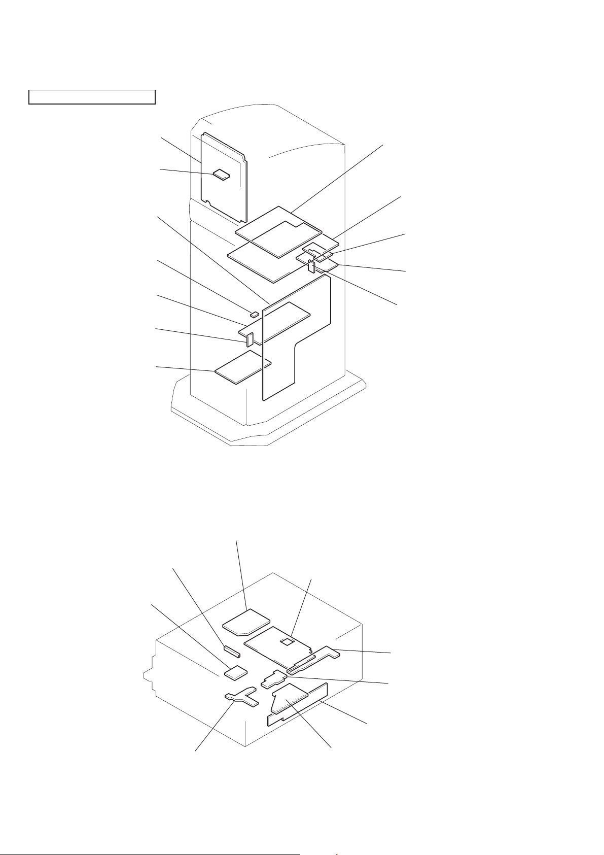
SECTION 2
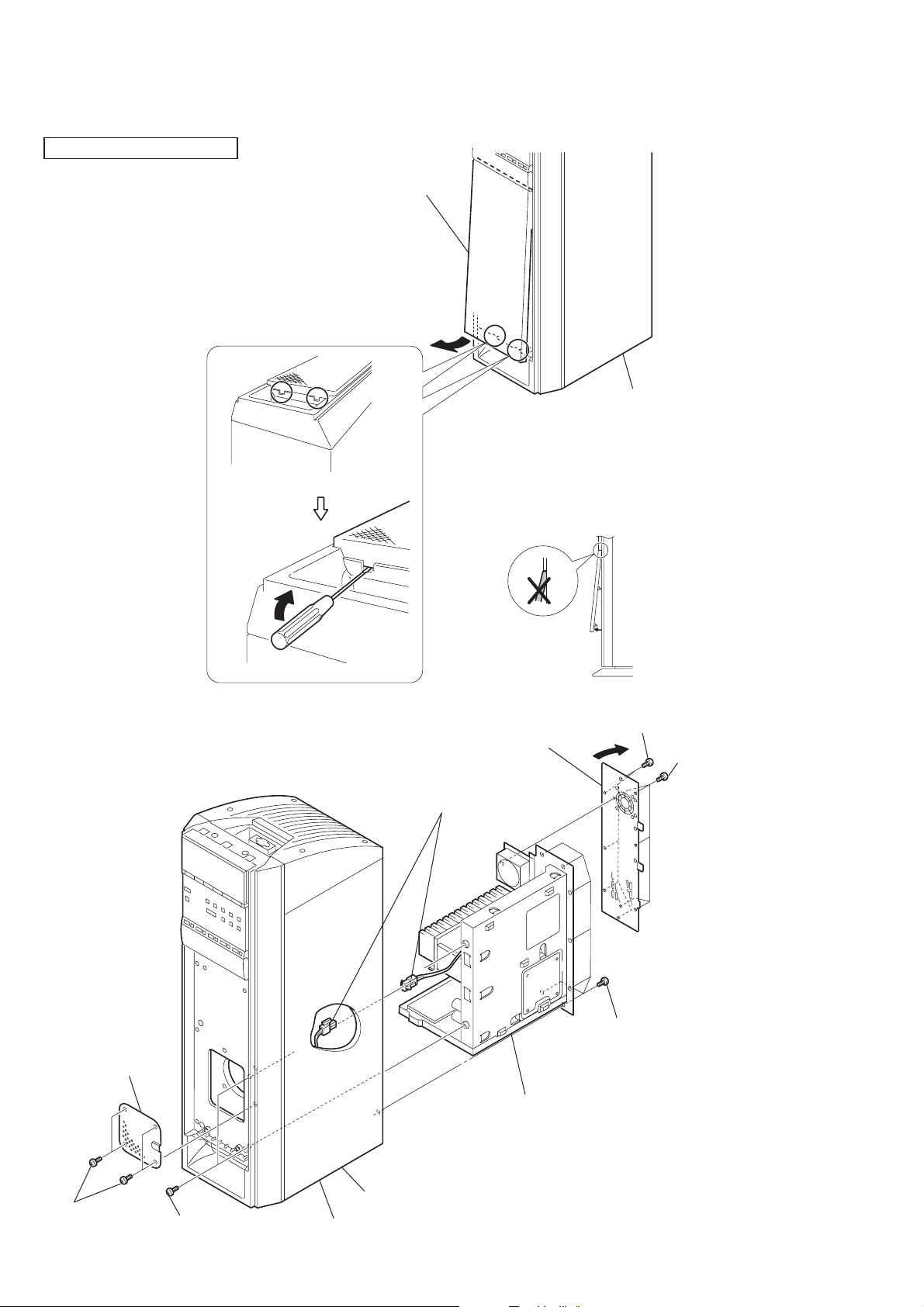
n
DISASSEMBLY
Note: Follow the disassembly procedure in the numerical order given.
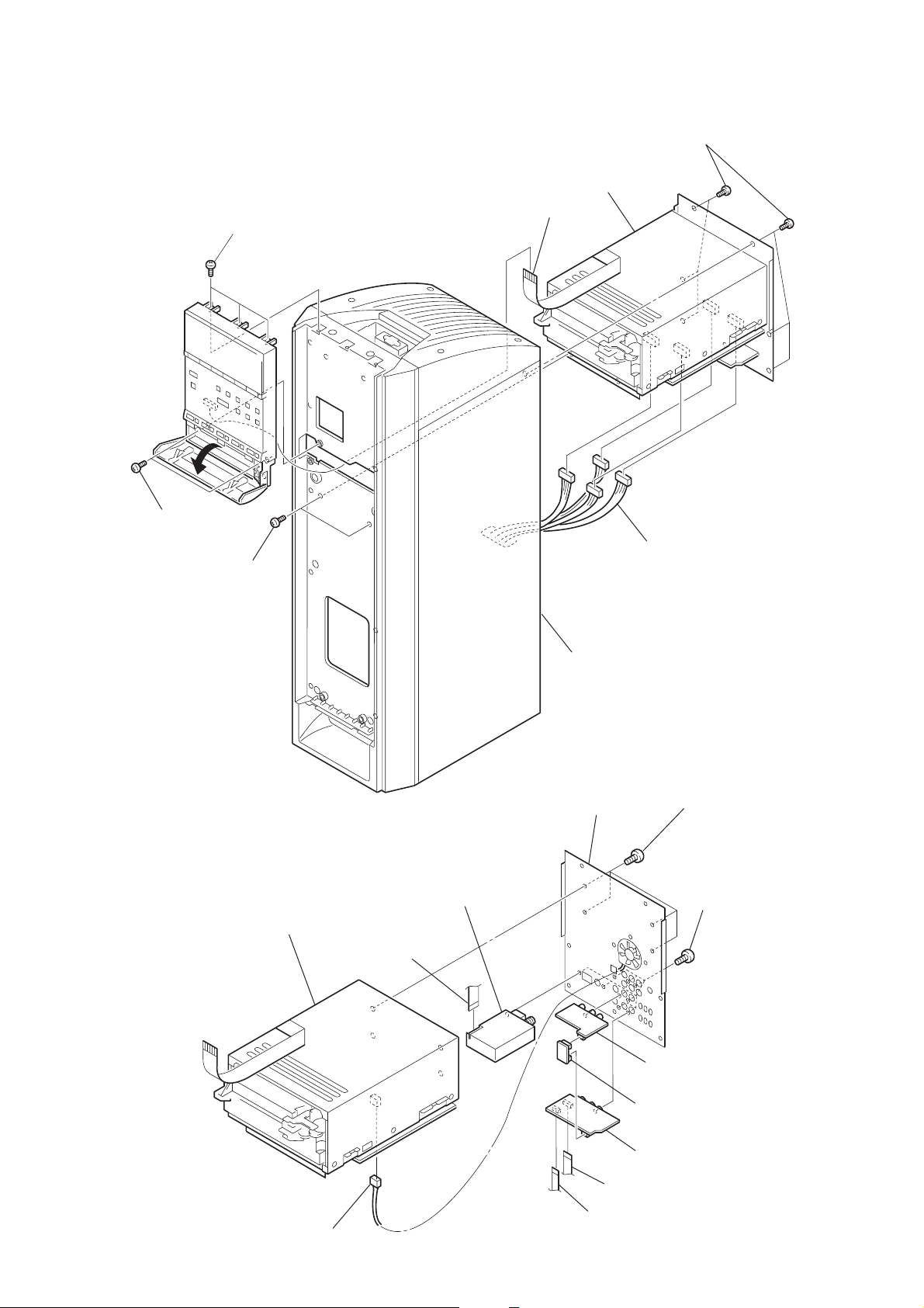
SAVA-D900 (MAIN UNIT)
2-1. GRILLE FRAME (B) ASSY
2
Grille frame (B) assy
1
Note : Be careful not to open
1
excessively as shown.
Main unit (L-ch) sectio
2-2. AMPLIFIER ASSY
2
Cover (BF)
FOR AMP ASSY
4
Five screws
(BVTT4
×
6
Back panel (L/B)
8
Connecter
FOR
9
Amplifier assy
7
20)
5
Five screws
(BVTP3
Seven screws
(BVTP4
×
20)
×
8)
6
1
Four screws
(P4
×
12)
3 Two screws
(BVTT4
×
25)
Main unit (L-ch) section
Main unit (L-ch) section
Page 7
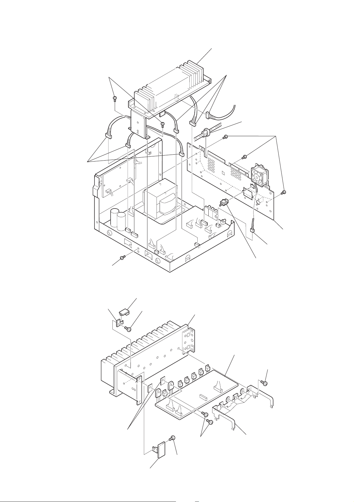
2-3. AMPLIFIER CHASSIS
7
Two screws
(transistor)
5
Connecters
0
Heatsink and AMP board
4
Connecters
3
Cord bushing
8
Twelve screws
(BVTP3
×
8)
2-4. AMP BOARD
6
Screw (BVTP3 × 8)
8
Bracket
9
THERMO board
7
Screw
(BVTP3
9
Back panel (L/A)
1
Connecter
2
Connecter
0
×
8)
Heatsink
4
AMP board
1
Six screws
(BVTP3
×
8)
Supplied with
Q1704, 1705
6
REG board
5
Screw
(BVTP3
3
Three screws
(transistor)
×
8)
2
Bracket
7
Page 8

)
2-5. POWER TRANSFORMER (T900)
1
Connector
3
Four screws
(BVTT4
×
8)
4
Power transformer (T900
2
Connectors
2-6. PS BOARD
5
STBY board
4
Four screws
(BVTP3 × 8)
2 Six
(BVTP3 × 8)
1
Connector
screws
3
PS board
8
Page 9
)
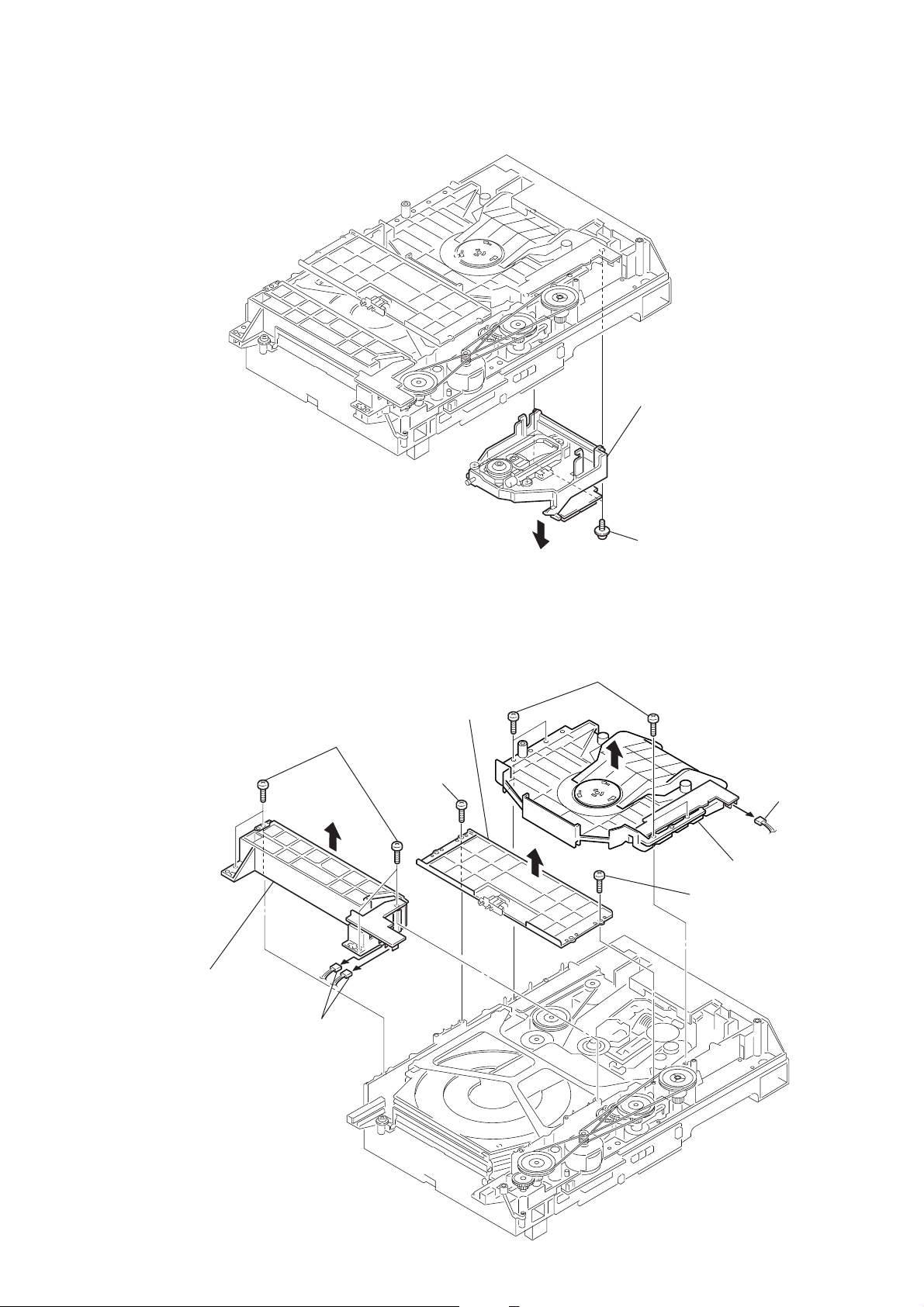
2-7. MECHANISM SECTION
1
3 screws
2
2 screws
(BVTP3
3
(BVTT4
(BVTP3
×
12)
2 screws
×
×
25)
12)
6
Flat wire
7
Mechanism section
4
Six screws
(BVTT4
5
Four connectors
×
20)
2-8. VIDEO BOARD
4
DVD section
5
Flat wire
6
TUNER unit
Main unit (L-ch) section
qs
Panel (L/C) back
2
Four screws
(BVTP3
3
0
Video board
9
V-connect board
×
8)
Nine screws
(BVTP3
×
8
1
Connector
8
7
Flat wire
qa
S-video board
Flat wire
9
Page 10

2-9. MAIN BOARD AND DVD BOARD
e
)
qf
DVD assy
7
6
qd
DVD board
Four screws
MAIN board
(BVTP3
2
Flat wire
×
8)
3
Flat wire
qs
Four screws (BVTP3 × 8)
qa
0
Connector
9
Flat wire
8
Bracket
5
Four screws
(BVTP3
Flat wire
4
Flat wir
×
8)
2-10. MECHANISM (CDM53J-DVBU1)
4
Two screws
(BVTP3 × 8)
5
Mechanism
(CDM53J-DVBU1)
3
Cover
1
Flat wire
1
Ten screws (BVTP3 × 8)
2
Four screws
(BVTP3 × 8
10
6
Chassis
Page 11
2-11. BASE UNIT (DVBU1)
r
2
Base unit (DVBU1)
1
Two screws
(PTPWH M2.6)
2-12. MAGNET ASSY
3
Fitting base
(guide) assy
2
Four screws
(BVTP M2.6)
1
Two connectors
(CN709, 715)
6
Bracket
(chassis)
4
Screw
(BVTP M2.6)
8
Four screws
(BVTP M2.6)
5
(BVTP M2.6)
Screw
7
Connecto
(CN710)
9
Magnet assy
11
Page 12
2-13. TRAY (SUB)
)
1 Turn the pulley (LD) and move the slider (selection) in the
direction of the arrow L.
2 Turn the pulley (mode) in the direction of the arrow to adjust
the tray (sub) that you want to remove.
(It depends on the height and position
of the stocker.)
3 Turn the pulley (LD) and move the slider
(selection) in the direction of the arrow R.
4 Turn the pulley (mode) in the direction of the arrow so
that you can remove the tray (sub) that you
want to remove.
Pully (LD)
Slider (selection)
Stocker section
Tray (sub)
L
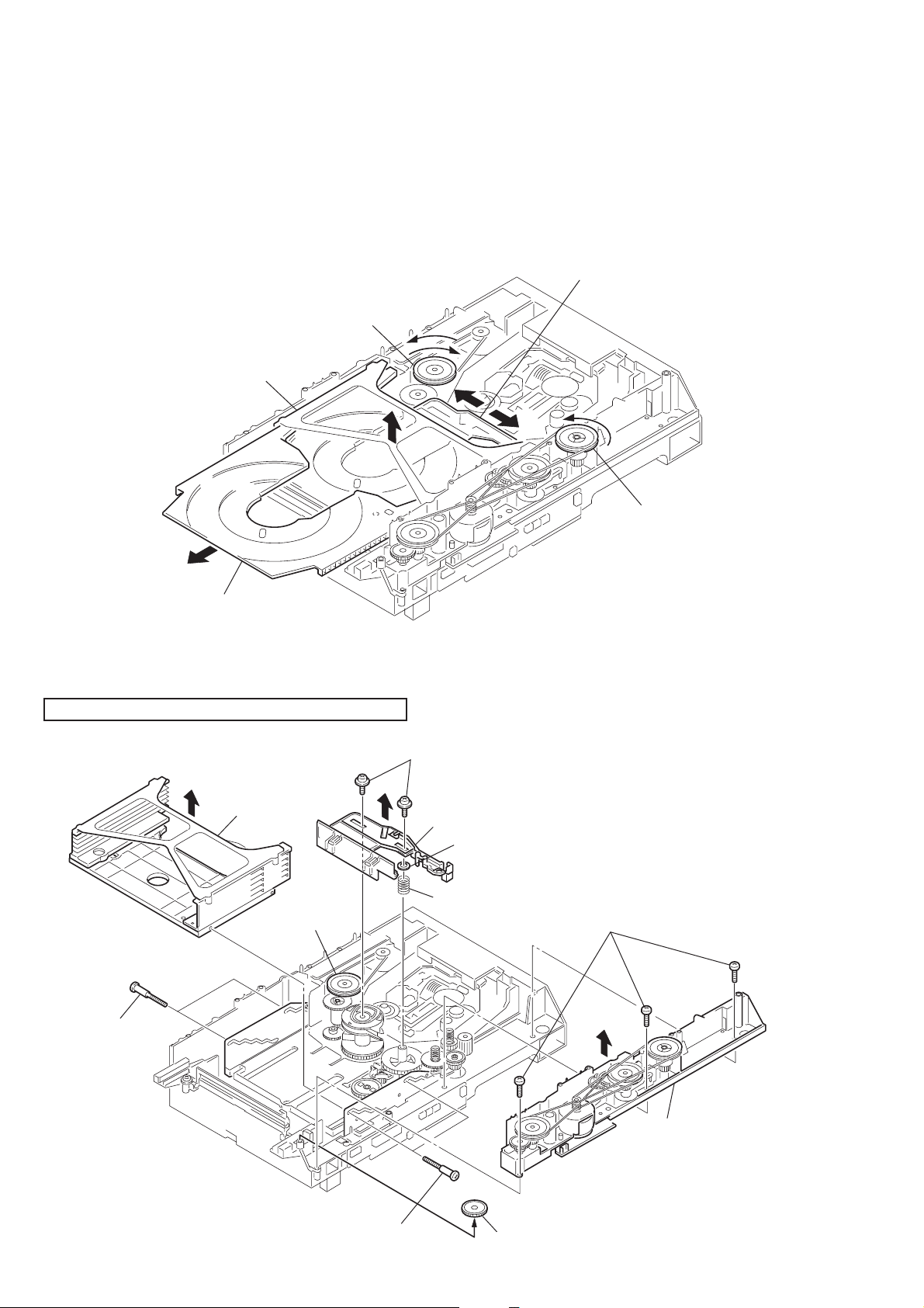
2-14. CHASSIS (MOLD B), STOCKER, SLIDER (SELECTION)
Note: When assembling the parts, refer to pages 13 and 14.
7
Two screws
(PTPWH M2.6)
6
Stocker
section
8
Slider (selection)
9
Washer
R
Pully (mode)
12
5
Two step
screws
Pully (LD)
4
Two step screws
0
Compression
spring
3
Gear (eject)
1
Three screws
(BVTP M2.6)
2
Note: Rotating the pully (LD),
shift the slider (selection
to the left.
Chassis (mold B) section
Page 13

2-15. HOW TO ASSEMBLE THE GEARS
3
Gear (gear B)
Portion A
Adjust the gear (gear B) with the
portion A as shown.
1
Slide the slider (u/d)
fully in the arrow
direction.
2
Gear (U/D slider)
Slider (U/D) gear
4
Gear (gear A)
Gear
(gear B)
Linearly
Adjust the gear so that it meshes with
the bottom tooth of slider (U/D) gear,
as shown.
2-16. HOW TO ATTACH THE SLIDER (SELECTION)
2
Gear (chuking)
Rotary encoder
Align with the slot of
rotary encoder.
6
Two screws
(PTPWH M2.6)
5
Washer
4
Compression spring
7
Insert the slider (selection)
into the portion A.
Adjust so as to be aligned with
gear B linearly, as shown.
Portion A
1
Rotary encoder
Align marking
3
Convex portion of
slider (selection)
Gear (chuking)
Insert a convex portion into
a groove of gear (chuking).
13
Page 14

2-17. HOW TO ATTACH THE STOCKER
1
Stocker section
2
Portion A of tray (sub)
Hook the portion A of tray (sub)
to the slider (selection).
3
Two step screws
2-18. HOW TO ATTACH THE CHASSIS (MOLD B)
3
Three screws
(BVTP M2.6)
Portion A
of tray (sub)
4
Two step screws
Sticking of
slider (selection)
14
2
Insert the gear (eject0
under the gear (LD
deceleration).
Gear (LD deceleration)
Portion A
Portion B of
slider (selection)
1
Insert the portion A of
chassis (mold B) section
into the portion B of
slider (selection).
Page 15

SECTION 3
TEST MODE
How to enter the test mode
Blue display (test mode)
DVD microprocessor downloading mode
All cliar of STR side
Key Check
Display Check
Speaker Check
* The speaker check mode is the test mode in which the sound signel that is input to the TV INPUT is output
from all speakers at the unity sound level.
• Selcting 9K or 10K of AM
Select the AM band. Turn off the main power . While pressing the SUB WOOFFER MODE button, press the ?/1
(power) switch to turn on the main power.
Order of pressing simultaneously
123
SWMODE
SWMODE
SWMODE
SWMODE
SWMODE
SWMODE
BAND
STOP
STOP
STOP
BAND
STOP
DISC 1
DISC 2
DISC 3
EJECT 3
EJECT 5
EJECT 4
Press to return
—
—
—
SAVA-D900’s key
STOP
STOP
15
Page 16

3-1. GENERAL DESCRIPTION
The T est Mode allows you to make dia gnosis and adjustment easily
using the remote commander and monitor TV. The instructions,
diagnostic results, etc. are given on the on-screen display (OSD).
3-2. STARTING TEST MODE
Set the FUNCTION to DVD with the main unit power on. Next,
while pushing the [STOP] button and the [MUTING] button on the
main unit at the same time, turn the regulator to the right to start
T est Mode and display the menu shown belo w on the TV screen. At
the bottom of the menu screen, the model name and revision number
are displayed.
To execute each function, select the desired menu and press its
number on the remote commander. To exit from Test Mode, press
the [POWER] button.
Test Mode Menu
0. Syscon Diagnosis
1. Drive Auto Adjustment
2. Drive Manual Operation
3. Mecha Aging
4. Emergency History
5. Version Information
6. Video Level Adjustment
Exit: Power Key
_
Model : HCX932xxxx
Revision: 1.xxx
3-3. SYSCON DIAGNOSIS
The same contents as board detail check by serial interface can be
checked from the remote commander.
On the Test Mode Menu screen, press
commander, and the following check menu will be displayed.
### Syscon Diagnosis ###
Check Menu
0. Quit
1. All
2. Version
3. Peripheral
4. Servo
5. Supply
6. AV Decoder
7. Video
8. Audio
_
0. Quit
Quit the Syscon Diagnosis and return to the Test Mode Menu.
1. All
All items continuous check
This menu checks all diagnostic items continuously. Normally, all
items are checked successively one after another automatically
unless an error is found, but at a certain item that requires judgment
through a visual check to the result, the following screen is displayed
for the key entry.
[0] key on the remote
### Syscon Diagnosis ###
Diag All Check
No. 2 Version
2-3. ROM Check Sum
Check Sum = 2005
Press NEXT Key to Continue
Press PREV Key to Repeat
_
For the ROM Check, the check sum calculated by the Syscon is
output, and therefore you must compare it with the specified value
for confirmation.
Following the message, press [NEXT] key to go to the ne xt item, or
[PREV] key to repeat the same check again. To quit the diagnosis
and return to the Check Menu screen, press [STOP] or
[ENTER] key. If an error occurred, the diagnosis is suspended and
the error code is displayed as shown below.
### Syscon Diagnosis ###
3-3. EEPROM Check
Error 03: EEPROM Write/Reed N
Address : 00000001
Write Data : 2492
Read Data : 2490
Press NEXT Key to Continue
Press PREV Key to Repeat
_
Press [STOP] key to quit the diagnosis, or [PREV] key to repeat
the same item where an error occurred, or [NEXT] key to continue
the check from the item next to faulty item.
Selecting 2 and subsequent items calls the submenu screen of each
item.
For example, if “5. Supply” is selected, the following submenu will
be displayed.
### Syscon Diagnosis ###
Check Menu
No. 5 Supply
0. Quit
1. All
2. ARP Register Check
3. ARP to RAM Data Bus
4. ARP to RAM Address Bus
5. ARP RAM Check
_
0. Quit
Quit the submenu and return to the main menu.
1. All
All submenu items continuous check
This menu checks 2 and subsequent items successively . At the item
where visual check is required for judgment or an error occurred,
the checking is suspended and the message is output for key entry.
Normally, all items are checked successively one after another
automatically unless an error is found.
16
Page 17
Selecting 2 and subsequent items executes respective menus and
outputs the results.
For the contents of each submenu, see “Check Items List”.
General Description of Checking Method
2. Version
(2-2) Revision
ROM revision number is displayed.Error: Not detected.
The revision number defined in the source file of ROM (At
the beginning of mass production, the Flash ROM of IC205
is used, but midway it is replaced by the IC206 OTP ROM.
IC205 or IC206) is displayed with four digits.
Below IC205 are all IC205 or IC206.
(2-3) ROM Check Sum
Check sum is calculated.
Error: Not detected.
The 8-bit data are added at addresses 0x000F0000 ~
0x002EFFFF of ROM (IC205) and the result is displayed
with 4-digit hexadecimal number. Error is not detected.
Compare the result with the specified value.
4. Servo
(4-2) Servo DSP Check
Data write → read, and accord check
Error 12: Read data discord
Data 0x9249, 0x2942, 0x4294 are written to the address
0x602 of RAM in the Servo DSP (IC701), then read and
checked.
(4-3) DSP Driver Test
Test signal data → DSP Driver
Error: Not detected.
Caution: Do not conduct this test with a mechanical deck
connected.
The maximum voltage is applied to the Servo Driver IC
(IC801, IC802). If mechanical deck is connected, the motor and optics could be damaged. Disconnect mechanical
deck following the output message, then enter specified 4or 5-digit number from the remote commander, and press
the [ENTER]. The test is conducted only when the input
data accord. Check the output level, then press the [NEXT]
to finish the test.
This test is skipped if “All” is selected.
(2-4) Model Type
Model code is displayed.
Error: Not detected.
The model code read from EEPROM (IC201) is displayed
with 2-digit hexadecimal number.
Model Type
SAVA-D900 20
(2-5) Region
Region code is displayed.
Error: Not detected.
The region code determined from the model code is displayed.
3. Peripheral
(3-2) Gate Array Check
Data write → read, and accord check
Error 02: Gate array write/read discord
Data 0x00~0xFF are written to the address 0xF of GA
(IC601), then read and checked if they accord.
(3-3) EEPROM Check
Data write → read, and accord check
Error 03: EEPROM write/read discord
Data 0x9249, 0x2942, 0x4294 are written to addresses
0x00~0xFF of EEPROM (IC201), then read and checked.
Before writing, the data are saved, then after checking, they
are written to restore the contents of EEPROM.
Supplement: How to disconnect mechanical deck
Disconnect flat cables connected to the CN002 and CN003
of MB-82/85 board. Also, disconnect harness from the
CN011.
5. Supply
Caution: Do not conduct this check with a mechanical deck
connected.
An access is made to the stream supply and servo control
IC (IC303) and external RAM (IC304) using check data.
If mechanical deck is connected, the motor and optics
could be damaged. This check is also executed by the “ All”
menu item.
Supplement: How to disconnect mechanical deck
Disconnect flat cables connected to the CN002 and
CN003 of DVD board. Also, disconnect harness from
the CN011.
(5-2) ARP Register Check
Data write → read, and accord check
Error 08: ARP register write, and read data discord
Data 0x00 to 0xFF are written to the TMAX register (address 0xC6) in ARP (IC303), then the y are read and checked.
(5-3) ARP to RAM Data Bus
Data write → read, and accord check
Error 09: ARP ←→ RAM data bus error
Data 0x0001 to 0x8000 where one bit each is set to 1 are
written to the address 0 of RAM (IC304) connected to the
ARP (IC303) through the bus, then they are read and
checked. In case of discord, written bit pattern and read
data are displayed. If data where multiple bits are 1 are
read, the bits concerned may touch each other. Further, if
data where certain bit is always 1 or 0 regardless of written
data, the line could be disconnected or shorted.
17
Page 18

(5-4) ARP to RAM Address Bus
Data write → other address read discord check
Error 10: ARP → RAM address bus error
Caution: Address and data display in case of an error is
different from the display of other diagnosis (de-
scribed later).
Before starting the test, all addresses of RAM (IC304) are
cleared to 0x0000.
First, 0xA55A is written to the address 0x00000, and the
address data are read and checked from addresses 0x00001
to 0x80000 while shifting 1 bit each. Next, the data at that
address is cleared, and it is written to the address 0x00001,
and read and checked in the same manner. This check is
repeated up to the address 0x80000 while shifting the address data by 1 bit each.
If data other than 0 is read at the addresses except written
address, an error is given because all addresses were already cleared to 0. In this check, the error display pattern is
different from that of other diagnosis; read data, written
address, and read address are displayed in this order. Ho wever , the message uses same template, and accordingly exchange Address and Data when reading. The following display, for example,
6. AV Decoder
(6-2) 1930 RAM
Data write → read, and accord check
Error 13: AVD RAM read data discord
The program code data stored in ROM (IC205) are copied
to all areas of RAM (IC402, IC403) connected to the AVD
(IC401) through the bus, then they are read and checked if
they accord. Further, the same test is conducted once again
with the data where all bits are inverted between 1 and 0. If
discord is detected, faulty address, written data, and read
data are displayed following the error code 13, and the test
is suspended.
(6-3) 1930 SP
ROM → AVD RAM → Video OUT
Error: Not detected.
The data including sub picture streams in ROM (IC205)
are transferred to the RAM (IC402, IC403) in AVD (IC401),
and output as video signals from the AVD (IC401).
They are output from all video terminals (Composite, Y/C).
7. Video
### Syscon Diagnosis ###
5-4. ARP to RAM Address Bus
Error 10: ARP - RAM Address B
Address : 0000A55A
Write Data : 00000000
Read Data : 00080000
Press NEXT Key to Continue
Press PREV Key to Repeat
_
shows the data 0xA55A was read from address 0x00080000
though it was written to the address 0x00000000. This implies that these addresses are in the form of shadow. Also,
if the read data is not 0xA55A, another error will be present.
(5-5) ARP RAM Check
Data write → read, and accord check
Error 11: ARP RAM read data discord
The program code data stored in ROM are copied to all
areas of RAM (IC304) connected to the ARP (IC303)
through the bus, then they are read and checked if they accord. If the detail check was selected initially, the data are
written to all areas and read, then the same test is conducted
once again with the data where all bits are inverted between
1 and 0. If discord is detected, faulty address, written data,
and read data are displayed following the error code 11,
and the test is suspended.
(7-2) Color Bar
AVD color bar command write → Video OUT
Error: Not detected.
The command is transferred to the AVD, and the color bar
signals are output from video terminals.
They are output from all video terminals (Composite, Y/C).
8. Audio
(8-2) ARP → 1930
Error 14 : ARP → 1930 video NG
15 : ARP → 1930 audio NG
18
Page 19

Check Items List
2) Version
(2-2) Revision
(2-3) ROM Check Sum
(2-4) Model Type
(2-5) Region
3) Peripheral
(3-2) Gate Array Check
(3-3) EEPROM Check
4) Servo
(4-2) Servo DSP Check
(4-3) DSP Driver Test
5) Supply
(5-2) ARP Register Check
(5-3) ARP to RAM Data Bus
(5-4) ARP to RAM Address Bus
(5-5) ARP RAM Check
6) AV Decoder
(6-2) 1930 RAM
(6-3) 1930 SP
7) Video
(7-2) Color Bar
Error Codes List
00: Error not detected
01: RAM write/read data discord
02: Gate array NG
03: EEPROM NG
08: ARP register read data discord
09: ARP ←→ RAM data bus error
10: ARP ←→ RAM address bus error
11: ARP RAM read data discord
12: Servo DSP NG
13: 1930 SDRAM NG
14: ARP → 1930 video NG
15: ARP → 1930 audio NG
16: 1910 UCODE download NG
17: System call error (function not supported)
18: System call error (parameter error)
19: System call error (illegal ID number)
20: System call error (time out)
90: Error occurred
91: User verification NG
92: Diagnosis cancelled
8) Audio
(8-2) ARP → 1930
(8-3) Test Tone
19
Page 20

3-4. DRIVE AUTO ADJUSTMENT
On the Test Mode Menu screen, press [1] key on the remote
commander, and the dri ve auto adjustment menu will be displayed.
## Drive Auto Adjustment ##
Adjustment Menu
0. ALL
1. DVD-SL
2. CD
3. DVD-DL
4. SACD
Exit: RETURN
Normally, [0] is selected to adjust DVD (single layer), CD, DVD
(dual layer), and SACD in this order. But, individual items can be
adjusted for the case where adjustment is suspended due to an error.
In this mode, the adjustment can be made easily through the
operation following the message displayed on the screen.
The disc used for adjustment must be the one specified for
adjustment. However, for SACD disc, use the player with initial
data if the disc is not available.
0. ALL
Select [0] and press [ENTER] key, and the servo set data in
EEPROM will be initialized. Then, 1. D VD-SL disc, 2. CD disc , 3.
DVD-DL disc, and 4. SACD disc are adjusted in this order. Each
time one disc was adjusted, it is ejected. Replace it with the specified
disc following the message. Though the message to confirm whether
discs other than SACD disc are adjusted is not displayed, you can
finish the adjustment if pressing the
adjustment of each disc, the measurement for disc type judgment is
made. As automatic adjustment does not judge the disc type unlik e
conventional models, take care not to insert wrong type discs. Also,
do not give a shock during adjustment.
[STOP] button. During
1. DVD-SL (single layer)
Select
[1], insert DVD single layer disc, and press [ENTER] key,
and the adjustment will be made through the following steps, then
adjusted values will be written to the EEPROM.
DVD Single Layer Disc Adjustment Steps
1. SLED TILT Reset
2. Disc Check Memory SL
3. Wait 300 msec
4. Set Disc Type SL
5. LD ON
6. Spdl Start
7. Wait 1 sec
8. Focus Servo ON 0
9. Auto Track Offset Adjust
10. CLVA ON
11. Wait 500 msec
12. Tracking ON
13. Wait 1 sec
14. Sled ON
15. Check CLV Lock
16. Auto LFO Adjust
17. Auto Focus Offset Adjust
18. Auto Tilt Position Adjust
19. Auto Focus Gain Adjust
20. Auto Focus Offset Adjust
21. EQ Boost Adjust
22. Auto LFO Adjust
23. Auto Track Gain Adjust, Search Check
24. 32Tj Fwd
25. 32Tj Rev
26. 500Tj Fwd
27. 500Tj Rev
28. All Servo Stop
29. Eep Copy Loop Filter Offset
20
Page 21

2. CD
3. DVD-DL (dual layer)
Select [2], insert CD disc, and press [ENTER] key, and the
adjustment will be made through the following steps, then adjusted
values will be written to the EEPROM.
CD Adjustment Steps
1. Sled Tilt Rest
2. Disc Check Memory CD
3. Wait 500 msec
4. Set Disc Type CD
5. LD ON
6. Spdl Start
7. Wait 500 msec
8. Focus Servo ON 0
9. Auto Track Offset Adjust
10. CLVA ON
11. Wait 500 msec
12. Tracking ON
13. (TC Display Start)
14. Wait 1 sec
15. Jitter Display Start
16. Sled ON
17. Check CLV ON
18. Auto LFO Adjust
19. Auto Focus Offset Adjust
20.
21. Auto Focus Gain Adjust
22. Auto Focus Offset Adjust
23. Eq Boost Adjust
24. Auto LFO Adjust
25. Auto Track Gain Adjust, Search Check
26. 32Tj Fwd
27. 32Tj Rev
28. 500Tj Fwd
29. 500Tj Rev
30. All Servo Stop
Select [3], insert D VD dual layer disc, and press [ENTER] key , and
the adjustment will be made through the following steps, then
adjusted values will be written to the EEPROM.
DVD Dual Layer Disc Adjustment Steps
1. Sled Tilt Reset
2. Disc Check Memory DL
3. Wait 500 msec
4. Set Disc Type DL
5. LD ON
6. Spdl Start
7. Wait 1 sec, Layer 1 Adjust
8. Focus Servo ON 0
9. Auto Track Offset Adjust
10. Clva ON
11. Wait 500 msec
12. Tracking ON
13. Wait 500 msec
14. Sled ON
15. Check CLV Lock
16. Auto Loop Filter Offset Auto Focus Adjust
17.
18. Auto Focus Gain Adjust
19. Auto Focus Offset Adjust
20. Eq Boost Adjust
21. Auto Loop Filter Offset
22. Auto Track Gain Adjust, Search Check
23. 32Tj Fwd
24. 32Tj Rev
25. 500Tj Fwd
26. 500Tj Rev, Layer 0 Adjust
27. Fj (L1 -> L0)
28. Auto Track Offset Adjust L0
29. Clva ON
30. Wait 500 msec
31. Tracking ON
32. Wait 500 msec
33. Sled ON
34. Check CLV Lock
35. Auto Focus Filter Offset
36. Auto Focus Adjust
37.
38. Auto Focus Gain Adjust
39. Auto Focus Offset Adjust
40. Eq Boost Adjust
41. Auto Loop Filter Offset
42. Auto Track Gain Adjust, Search Check
43. 32Tj Fwd
44. 32Tj Rev
45. 500Tj fwd
46. 500Tj Rev, Layer Jump Check
47. Lj (L0 -> L1)
48. Lj (L1 -> L0)
49. All Servo Stop
21
Page 22

4. SACD
3-5. DRIVE MANUAL OPERATION
Select [4], insert SACD disc, and press [ENTER] key, and the
adjustment will be made through the following steps, then adjusted
values will be written to the EEPROM. However, if SACD disc is
not available, use the player with initial data, skipping the SACD
adjustment. In this case, you can finish the adjustment if pressing
the [STOP] button.
SACD Adjustment Steps
1. Sled Tilt Reset
2. Set Disc Type CD
3. LD ON
4. Spdl Start
5. Wait 500 msec
6. Focus Servo ON 0
7. Auto track Offset Adjust
8.
9. CLVA ON
10. Wait 500 msec
11. Tracking ON
12. Wait 1 sec
13. Sled ON
14. Check CLV ON
15. Auto Focus Offset Adjust
17.
18. Auto Focus Gain Adjust
19. Auto Focus Offset Adjust
20. Eq Boost Adjust
21. Auto LFO Adjust
22. Auto Track Gain Adjust
23. 32Tj Fwd
24. 32Tj Rev
25. 500Tj Fwd
26. 500Tj Rev
On the T est Mode Menu screen, select [2], and the manual operation
menu will be displayed. For the manual operation, each servo on/
off control and adjustment can be executed manually.
## Drive Manual Operation ##
Operation Menu
1. Disc type
2. Servo Control
3. Track/Layer Jump
4. Manual Adjustment
5. Auto Adjustment
6. Memory Check
0. Disc Check Memory
Exit: Return
In using the manual operation menu, take care of the following
points. These commands do not provide protection, thus requiring
correct operation. The sector address or time code field is displayed
when a disc is loaded.
1. Set correctly the disc type to be used on the Disc Type
screen.
The disc type must be set after a disc was loaded.
The set disc type is cleared when the tray is opened.
2. After power ON, if the Drive Manual Operation was
selected, first perform “Reset SLED TILT” by opening 1.
Disc Type screen.
3. In case of an alarm, immediately press the [STOP] button
to stop the servo operation, and turn the power OFF.
Basic operation (controllable from front panel or remote
commander)
27. All Servo Stop */
[POWER] Power OFF
[STOP] Servo stop
[OPEN/CLOSE] Stop+Eject/Loading
[RETURN] Return to Operation Menu or Test Mode
Menu
[NEXT], [PREV] Transition between sub modes of menu
[1] to [9], [0] Selection of menu items
Cursor UP/DOWN Increase/Decrease in manually adjusted
value
22
Page 23

0. Disc Check Memory
Disc Check
1. SL Disc Check
2. CD Disc Check
3. DL Disc Check
0. Reset SLED TILT
1. Disc Type Auto Check
Disc Type
2. DVD SL 12 cm
3. DVD DL 12 cm
4. CD 12cm
5. SACD 12 cm
6. dvd SL 8 cm
7. DVD DL 8 cm
8. CD 8 cm
9. SACD 8 cm
0. Reset SLED TILT
TC. : : EMG. 00
CD 12 cm
Display when CD 12cm disc was selected
On this screen, the mirror time is measured to judge the disc and it
is written to the EEPROM. First load DVD SL disc and press [1],
next load CD disc and press [2], and finally load D VD DL disc and
press [3].
The adjustment must be executed more than once after default data
were written. External vibration or shock to the player must not be
given. Reference value for D VD is from 10 to 20, and for CD, from
28 to 4F.
Check that the value of CD is larger than that of DVD.
When those values are beyond a range perform this adjustment again.
From this screen, you can go to another mode by pressing [NEXT]
or [PREV] key, but you cannot enter this mode from another mode.
You can enter this mode from the Operation Menu screen only.
1. Disc Type
Disc Type
1. Disc Type Auto Check
2. DVD SL 12 cm
3. DVD DL 12 cm
4. CD 12cm
5. SACD 12 cm
6. dvd SL 8 cm
7. DVD DL 8 cm
8. CD 8 cm
9. SACD 8 cm
0. Reset SLED TILT
EMG. 00
[0] Reset SLED TIL T Reset the Sled and Tilt to initial position.
[1] Disk Type Check Judge automatically the loaded disc. As
the judged result is displayed at the
bottom of screen, make sure that it is
correct.
If Disc Check Memory menu has not
been executed after EEPROM default
setting, the disc type cannot be judged.
In this case, return to the initial menu
and make a check for three types of discs
(SL, DL, CD).
[2] to [9] Select the loaded disc. The adjusted
value is written to the address of selected
disc. No further entry is necessary if [1]
was selected.
2. Servo Control
Servo Control
1. LD Off R.Sled FWD
2. SP Off L.Sled REV
3. Focus Off
4. TRK. Off
5. Sled Off
6. CLVA Off
7. FCS. Srch Off
On this screen, select the disc type. T o select the disc type, press the
number of the loaded disc. The selected disc type is displayed at the
bottom. Selecting [1] automatically selects and displays the disc
type. In case of wrong display, retry “Disc Check Memory”. Also,
opening the tray causes the set disc type to be cleared. In this case,
set the disc type again after loading.
In performing manual operation, the disc type must be set.
Once the disc type has been selected, the sector address or time
code display field will appear as shown below. These values are
displayed when PLL is locked.
Disc Type
1. Disc Type Auto Check
2. DVD SL 12 cm
3. DVD DL 12 cm
4. CD 12cm
5. SACD 12 cm
6. dvd SL 8 cm
7. DVD DL 8 cm
8. CD 8 cm
9. SACD 8 cm
0. Reset SLED TILT
SA. SI. EMG. 00
DVD SL 12 cm
Display when DVD SL 12cm disc was selected
0. Reset SLED TILT
SA. SI. EMG. 00
DVD SL 12 cm
On this screen, the servo on/off control necessary for replay is
executed. Normally, turn on each servo from 1 sequentially and
when CLVA is turned on, the usual trace mode becomes active. In
the trace mode, DVD sector address or CD time code is displayed.
This is not displayed where the spindle is not locked.
The spindle could run overriding the control if the spindle system is
faulty or RF is not present. In such a case, do not operate CLVA.
23
Page 24

[0] Reset SLED TILT Reset the Sled and Tilt to initial position.
3-6. MECHA AGING
[1] LD Turn ON/OFF the laser.
[2] SP Turn ON/OFF the spindle.
[3] Focus Search the focus and turn on the focus.
[4] TRK Turn ON/OFF the tracking servo.
[5] Sled Turn ON/OFF the sled servo.
[6] CLVA Turn ON/OFF normal servo of spindle
servo.
[7] FCS. Srch Apply same voltage as that of focus
search to the focus drive to check the
focus drive system.
→ Sled FWD Move the sled outward. Perform this
operation with the tracking servo turned
off.
← Sled REV Move the sled inward. Perform this
operation with the tracking servo turned
off.
↑ Tilt UP Move the tilt upward.
### Mecha Aging ###
1. TRAY Aging
2. SEARCH Aging
Abort: STOP key
On the T est Mode Menu Screen, selecting [3] e xecutes the aging of
the mechanism. TRAY aging or SEARCH aging are selected by [1]
or [2]. Start aging with PLAY. During aging, the repeat cycle is
displayed. Aging can be aborted at an y time by pressing the [STOP]
key. After the operation is stopped, press the [STOP] key or
[RETURN] key again to return to the Test Mode Menu. SEARCH
Aging is only for a CD.
3-7. EMERGENCY HISTORY
### MEG. History ###
Laser Hours CD xxxxxxxh
DVD xxxxxxxh
↓ Tilt DOWN Move the tilt downward.
The following menus are normally not used.
3. Track/Layer Jump
4. Manual Adjustment
5. Auto Adjustment
The persons who do not know well about these menus should not
use them.
6. Memory Check
EEPROM DATA
CD – DVD –
ID No. 00 SACD SL L0 L1
Focus Gain xx xx xx xx xx
TRK. Gain xx xx xx xx xx
Focus Offset xx xx xx xx xx
TRK. Offset xx xx xx xx xx
L. F. Offset xx xx xx xx xx
EQ Boost xx xx xx xx xx
Jitter xx xx xx xx xx
Mirror Time xx xx xx xx xx
_
CLEAR: Default Set
This screen displays current servo adjusted data stored in the
EEPROM. Though adjusted data can be initialized with the [CLEAR]
key, they cannot be restored after initialization.
So, before clearing, make a note of the adjusted data.
For reference, the drive has been designed so that the gain center
value is 20 and offset v alue is 80. Other v alues will be in a range of
10 to 80. If extreme value such as 00 or FF is set, adjustment will be
faulty . In such a case, check for disc scratch or cable disconnection,
then perform adjustment again.
1. 00 00 00 00 00 00 00 00
00 00 00 00 00 00 00 00
2. 00 00 00 00 00 00 00 00
00 00 00 00 00 00 00 00
Select: 1 – 9 Scroll: UP/DOWN
(1: Last EMG.) Exit: Return
On the Test Mode Menu screen, selecting [4] displays the
information such as servo emergency history. The history
information from last 1 up to 10 can be scrolled with
↑
key or
↓
key . Also, specific information can be displayed by directly entering
that number with ten keys.
The upper two lines display the laser ON total hours. Data below
minutes are omitted.
Clearing History Information
Clearing laser hours
Press [DISPLAY] and [CLEAR] keys in this order.
Both CD and DVD data are cleared.
Clearing emergency history
Press [TITLE] and [CLEAR] keys in this order.
Initializing set up data
Press [DVD] and [CLEAR] keys in this order.
The data have been initialized when “Set Up Initialized” message
is displayed. The EMG. History screen will be restored soon.
24
Page 25

How to see Emergency History
1.0 ± 0.02 Vp-p
3-8. VERSION INFORMATION
31.12
2
1 : Emergency Code
2 : Don’t Care
These codes are used for verification of software designing.
3 : Historical order 1 to 9
Emergency Codes List
10: Communication to IC001 (TK board) failed.
11: Each servo for focus, tracking, and spindle is unlocked.
12: Communication to EEPROM, IC201 (DVD board) failed.
13: Writing of hours meter data to EEPROM, IC201 (DVD board)
failed.
14: Communication to Servo DSP IC701 (DVD board) failed, or
Servo DSP is faulty.
20: Initialization of tilt servo and sled servo failed. They are not
placed in the initial position.
21: Tilt servo operation error
22: Syscon made a request to move the tilt servo to wrong posi-
tion.
23: Sled servo operation error
24: Syscon made a request to move the sled servo to wrong posi-
tion.
30: Tracking balance adjustment error
31: Tracking gain adjustment error
32: Focus balance adjustment error
33: Focus bias adjustment error
34: Focus gain adjustment error
35: Tilt servo adjustment error
36: RF equalizer adjustment error
37: RF group delay adjustment error
38: Jitter value after adaptive servo operation is too large.
40: Focus servo does not operate.
41: With a dual layer (DL) disc, focus jump failed.50: CLV
(spindle) servo does not operate.
51: Spindle does not stop.
60: With a DVD disc, Syscon made a request to seek nonexistent
address.
61: With a CD disc, Syscon made a request to seek nonexistent
address.
62: With a CD disc, Syscon made a request to seek nonexistent
track No. and index No.
63: With a DVD disc, seeking of target address failed.
64: With a CD disc, seeking of target address failed.
65: With a CD disc, seeking of target index failed.
70: With a DVD disc, physical information data could not be read.
71: With a CD disc, TOC data could not be read.
80: Disc type judgment failed.
81: As disc type judgment failed, retry was repeated.
82: As disc type judgment failed, a measurement error occurred.
83: Disc type could not be judged within the specified time.
84: Illegal command code was received from Syscon.
85: Illegal command was received from Syscon.
## Version Information ##
IF con. Ver. x. xxx (xxxx)
Group 00
SYScon. Ver. x. xxx (xxxx)
Model xx
Region 0x
SW1 ??
SW2 ??
Exit: RETURN
On the Test Mode Menu screen, selecting [5] displays the ROM
version and region code.
The parenthesized hexadecimal number in version field is checksum
value of ROM.
3-9. VIDEO LEVEL ADJUSTMENT
On the Test Mode Menu screen, selecting [6] displays color bars
for video level adjustment. During display of color bars, OSD
disappears but the menu screen will be restored if pressing any key.
Measurement point : LINE OUT VIDEO
(75 Ω terminating resistance)
Measuring instrument : Oscilloscope
Adjustment device : RV401 on DVD board
Specified value :1.0 ± 0.02 Vpp
25
Page 26

SECTION 4
ELECTRICAL ADJUSTMENTS
In making adjustment, refer to 4-2. Adjustment
Related Parts Arrangement.
Note: During diagnostic check, the characters and color bars can
be seen only with the NTSC monitor. Therefore, for
diagnostic check, use the monitor that supports both NTSC
and PAL modes
This section describes procedures and instructions necessary for
adjusting electrical circuits in this set.
Instruments required:
1) Color monitor TV
2) Oscilloscope 1 or 2 phenomena, band width over 100 MHz,
with delay mode
3) Frequency counter (over 8 digits)
4) Digital voltmeter
5) Standard commander
* RM-SS300 (1-418-838-11)
6) DVD reference disc
HLX-501 (J-6090-071-A) (dual layer)
HLX-503 (J-6090-069-A) (single layer)
HLX-504 (J-6090-088-A) (single layer)
HLX-505 (J-6090-089-A) (dual layer)
7) SACD reference disc
HLXA-509 (J-6090-090-A)
4-1. ADJUSTMENT OF VIDEO SYSTEM
1. Video Level Adjustment (DVD BOARD)
<Purpose>
This adjustment is made to satisfy the NTSC standard, and if not
adjusted correctly, the brightness will be too large or small.
Mode Video level adjustment in test mode
Signal Color bars
Test point
Instrument Oscilloscope
Adjusting element RV401
Specification 1.0 ± 0.02 Vp-p
Adjusting method:
1) Set so that color bars are generated.
2) Adjust the RV401 to attain 1.0 ± 0.02 Vp-p.
LINE OUT (VIDEO) connector
(75 Ω terminated)
1.0 ± 0.02 Vp-p
* Use only the designated remote control when adjusting this
system component.
2. S-terminal Output Check (DVD BOARD)
<Purpose>
Check S-terminal video output. If it is incorrect, pictures will not
be displayed correctly in spite of connection to the TV with a Sterminal cable.
Mode Video level adjustment in test mode
Signal Color bars
Test point
Instrument Oscilloscope
Specification 1.0 ± 0.1 Vp-p
Checking method:
1) Set so that color bars are generated.
2) Confirm that the S-Y level is 1.0 ± 0.1 Vp-p.
S VIDEO OUT (S-Y) connector
(75 Ω terminated)
1.0 ± 0.1 Vp-p
26
Page 27

3. Checking S Video Output S-C (DVD BOARD)
<Purpose>
This checks whether the S-C satisfies the NTSC Standard. If it is
not correct, the colors will be too dark or light.
Mode Video level adjustment in test mode
Signal Color bars
Test point CN005 pin 6
Instrument Oscilloscope
Specification 286 ± 50 mVp-p
Connection:
4-2. ADJUSTMENT RELATED PARTS
ARRANGEMENT
DVD BOARD (SIDE A)
CN005
2
1
RV401
VIDEO LEVEL ADJ
6
7
6
5
CN005
Oscilloscope
75Ω
±1%
100µF
+
100k
±1%
Checking method:
1) Confirm that the S-C burst is 286 ± 50 mVp-p.
286 ± 50 mVp-p
27
Page 28
5-1. CIRCUIT BOARDS LOCATION
d
d
SAVA-D900 (MAIN UNIT)
SECTION 5
DIAGRAMS
DISP board
FFC board
PS board
THERMO board
AMP board
REG board
STBY board
DVD board
MAIN board
VIDEO board
S-VIDEO board
V-CONNECT boar
• Mechanism section (CDM53J-DVBU1)
CLAMP MOTOR board
SENSOR 2 board
SENSOR board
OUT SW board
TK board
IN SW board
INT/COUNT SW boar
CONNECTOR board
LOAD MOTOR board
28
Page 29
SAVA-D900/D900FR/D900R/SS-T900
THIS NOTE IS COMMON FOR PRINTED WIRING
BOARDS AND SCHEMATIC DIAGRAMS.
(In addition to this, the necessary note is printed
in each block.)
For schematic diagrams.
Note:
• All capacitors are in µF unless otherwise noted. pF: µµF
50 WV or less are not indicated except for electrolytics
and tantalums.
• All resistors are in Ω and 1/
specified.
f
•
• 2 : nonflammable resistor.
• 5 : fusible resistor.
• C : panel designation.
• U : B+ Line.
• V : B– Line.
• H : adjustment for repair.
• Voltages and waveforms are dc with respect to ground
• Voltages are taken with a VOM (Input impedance 10 MΩ).
• Waveforms are taken with a oscilloscope.
• Circled numbers refer to waveforms.
• Signal path.
: internal component.
Note: The components identified by mark 0 or dotted line
with mark 0 are critical for safety.
Replace only with part number specified.
under no-signal (detuned) conditions.
Voltage variations may be noted due to normal production tolerances.
Voltage variations may be noted due to normal production tolerances.
no mark : FM
( ) : DVD PLAY
J : DVD/CD
c : AUDIO (digital)
g : VIDEO
L : C
F : Y
f : FM
4
W or less unless otherwise
For printed wiring boards.
Note:
• X : parts extracted from the component side.
a
•
• b : Pattern from the side which enables seeing.
: Through hole.
• Indication of transistor
C
Q
C
EB
These are omitted
These are omitted
EB
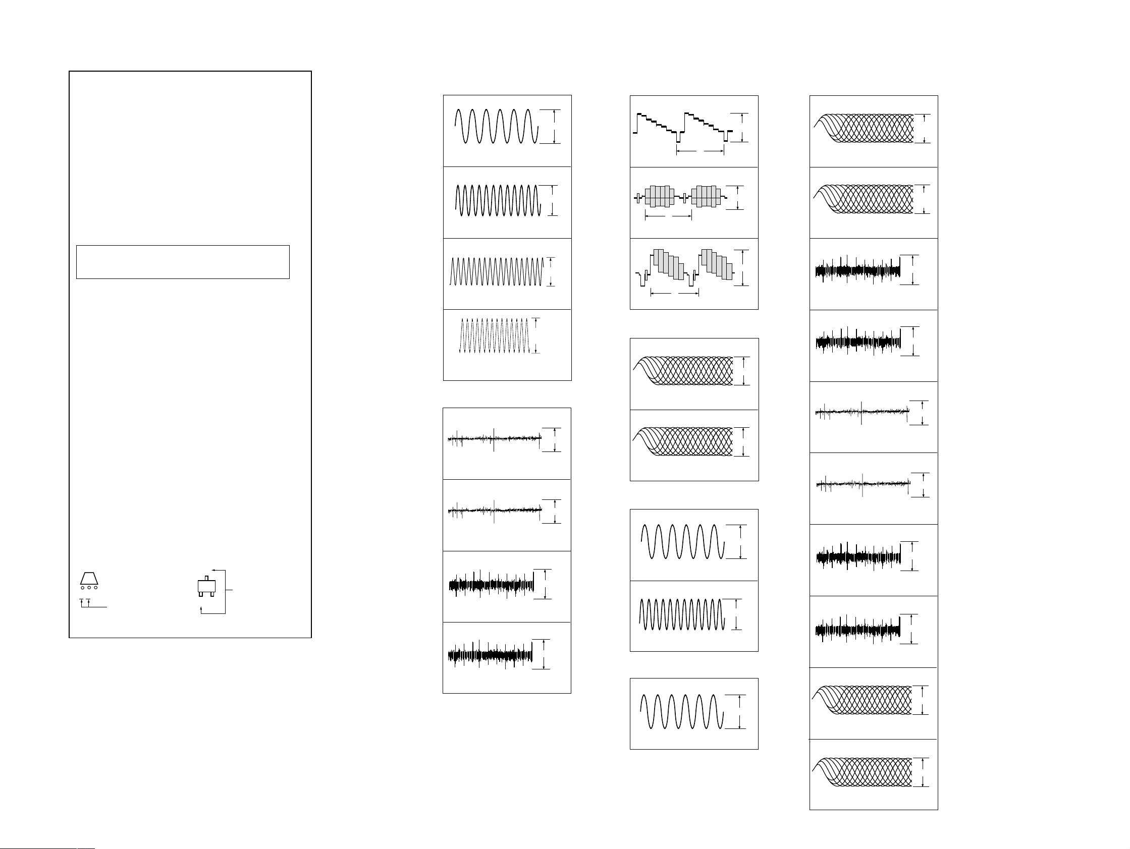
WAVEFORMS
– DVD (1/12) SECTION –
1
3.4Vp-p
27.0MHz
IC001 6
2
2.1Vp-p
33.8MHz
IC001 qs
3
2.8Vp-p
24.5MHz
IC001 qd
4
2Vp-p (DVD)
2.4Vp-p (CD)
DVD : 36.8MHz
CD : 33.8MHz
IC001 qj
– DVD (2/12) SECTION –
5
1.4Vp-p
500mV/DIV 50ms/DIV
IC701 yl DVD PLAY
6
1.7Vp-p
500mV/DIV 200ms/DIV
IC701 yl CD PLAY
7
220mVp-p
100mV/DIV 50ms/DIV
IC701 yk DVD PLAY
8
440mVp-p
500mV/DIV 50ms/DIV
IC701 yk CD PLAY
– DVD (4/12) SECTION –
9
1.0Vp-p
H
IC401 ya
q;
0.75Vp-p
H
IC401 ys
qa
1.2Vp-p
H
IC401 yg
– DVD (5/12) SECTION –
qs
1.5Vp-p
500mV/DIV 100ns/DIV
IC303 qj DVD PLAY
qd
1.5Vlp-p
500mV/DIV 500ns/DIV
IC303 ql CD PLAY
– DVD (8/12) SECTION –
qf
2.1Vp-p
12.4MHz
IC202 os
qg
2.5Vp-p
24.9MHz
IC202 5
– DVD (10/12) SECTION –
qh
1.8Vp-p
16MHz
IC903 qg
– TK SECTION –
1
200mV/DIV 100ns/DIV
IC001 1 DVD PLAY
2
500mV/DIV 500ns/DIV
IC001 1 CD PLAY
3
200mV/DIV 500ms/DIV
IC001 wl DVD PLAY
4
200mV/DIV 20ms/DIV
IC001 wl CD PLAY
5
500mV/DIV 50ms/DIV
IC001 el DVD PLAY
6
500mV/DIV 200ms/DIV
IC001 el CD PLAY
7
100mV/DIV 50ms/DIV
IC001 r; DVD PLAY
8
500mV/DIV 50ms/DIV
IC001 r; CD PLAY
9
500mV/DIV 100ns/DIV
IC001 tf DVD PLAY
q;
536
mVp-p
880
mVp-p
592mVp-p
448mVp-p
1.3Vp-p
1.7Vp-p
180mVp-p
860mVp-p
1.5Vp-p
1.5Vp-p
500mV/DIV 500ns/DIV
IC001 tf CD PLAY
2929
Page 30
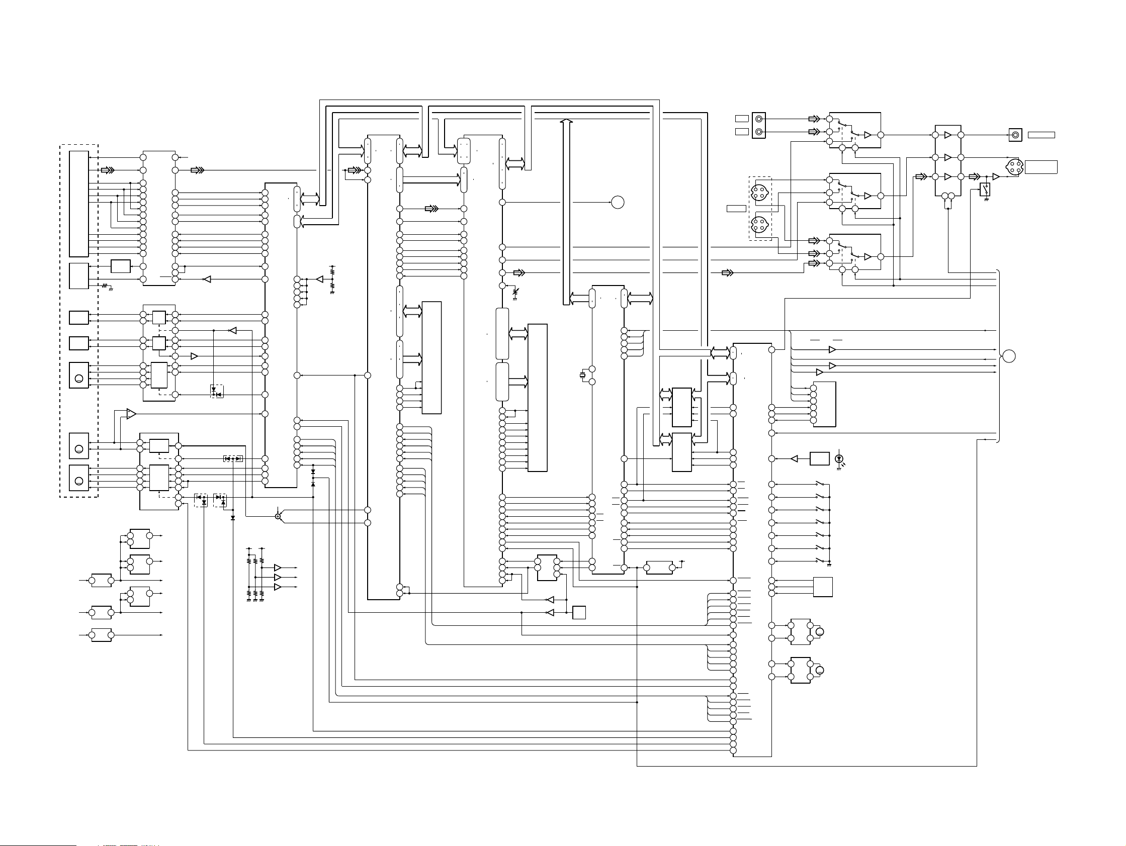
SAVA-D900/D900FR/D900R/SS-T900
5-2. BLOCK DIAGRAMS
– DVD SECTION –
OPTICAL DEVICE
DVD/CD
PDIC
DVD/CD
LD MOD
FOCUS
COIL
TRACKING
COIL
TILT
MOTOR
SPINDLE
MOTOR
SLED
MOTOR
16
D+5V
F
F
F
IC203
12 11
13
46
6
IC201
IC201
5
EEPROM
4
3
8
1
D SENSOR
Q703
S707
ROTARY
ENCODER
M
M
LOADING
1
3
5
1
3
5
1
3
5
M701
CLAMP
MOTOR
M702
MOTOR
IC1101 VIDEO SWJ1102
2
2
2
+5V
S701
MID OUT
S703
MID IN
S708
OUT
S704
IN
S705
INIT
S706
COUNT
S702
LID
4
IC1102 Y SW
4
IC1103 C SW
4
D704
IC1104
MUTE
3 10
151
g
134
V MUTE
V SEL2
V SEL1
XIFOK
XVIFCS
IFSO0
IFSC0
XIFINT
XFRRST
IFSI0
Q1101
Q1805
Q1806
MAIN
SECTION
117
7
g
FF
7
7
J1103
MONITOR OUT
Y
J1105
MONITOR OUT
(S-VIDEO)
C
B
VIDEO
g
HD8-15
HA0-5,17-19
XARPIT
XARPWT
XARPWR
XARPRD
XARPCS
XARPRST
DFCT
NORF
FWON
MD2
MUTE
XSDPIT
XSDPRD
XSDPWR
XSDPCS
XSDPRST
INPUT
F
J1104
S-VIDEO
INPUT
133
126
154
146
124
125
112
113
4
141
142
144
143
145
157
156
155
3
135
72
107
108
109
110
111
106
59
103
102
104
99
98
105
54
115
117
116
118
114
93
57
91
92
AUX
IC601
HGA
HD0
HD7
HA0-5
HA17-19
XRAMUB
XRAMLB
XRAMOE
XRAMWE
XFBSY
CS1
CS4
HWRH
HWRL
HRD
WAIT
XINT1
XINT3
RST
CPUCK
AVDWT
ARPINT
ARPWT
ARPWR
ARPRD
ARPCS
ARPRST
MCK
DFCT
NORF
FWON
MD2
MUTE
LOCK
FCSON
SDPIT
SDPRD
SDPWR
SDPCS
SDPRST
XDRV MUTE
SPDL STOP
LDMN/DMM
LDMP/DMP
XECS
XEWC
XEBSY
DSW1
CKSW1
EXP2
CKSW2
DOOPN
SSW1
SSW2
SSW3
CKMP
CKMM
g
Y
C
Y
C
VS
EXPI
CS0L
53
SI0
SO0
SC0
SI0
SO0
SC0
23
24
25
22XIFINT
Q701
68
84
88
85
83
64
63DOCLS
73EXPI0
67
66
65
IC701
90
367
MOTOR
DRIVE
89
69TRMP
70TRMP
IC702
367
MOTOR
DRIVE
2
2
IC303
IC001
DVD/CD RF AMP
VC
RF
A
B
C
D
E
F
G
H
LD
DRIVER
PD
VR
F+
F-
T+
T-
TA+
TA-
TB+
M
TB-
SP+
SP-
M
SLA+
SLA-
SLB+
M
SLB-
IC501
+5V
1 3
REG
IC002
+5V
1 3
REG
IC905
+3.3V
1 3
REG
¥
Signal path.
J
: DVD/CD
c
: AUDIO (Digital)
g
: VIDEO
L
: C
F
: Y
DIGITAL SERVO
17
VC
1
RF IP
Jc
12
A
11
B
10
C
9
D
5
2A
6
2B
7
2C
8
2D
13
E
14
F
15
G
16
LD
IC803
12
13
514
514
514
IC302
+3.3V
IC302
+3.3V
IC005
+3.3V
14
16
15
14
13
12
11
REG
REG
REG
H
20
LD
19
PD
COIL/MOTOR
14
13
12
11
17
18
MOTOR
15
14
SPINDLE/SLED
MOTOR DRIVE
SPINDLE
MOTOR
MOTOR
IC801
DRIVE
F COIL
DRIVE
T COIL
DRIVE
TILT
DRIVE
IC802
DRIVE
SLED
DRIVE
Q001
SIGO
SCLK
SDEN
HOLD2
FDCHG
CLOCK
TZC
SWD
SRD
DFT
+3.3V
IC303
+3.3V
IC401
+5VA+10V
+3.3V
A+5V+12V
+3.3V
IC903
2VC
VCI
33
54
FE
40
TE
39
PI
29
26MIRR
32
43
44
45
46
42
31
Q002
27
2
3
9
5
6
IC702
7
23
26
20
26
20
3
6
5
2
D803 D804
9
23
Q801
13
D805
D801
D802
+3.3V
IC701
SERVO DSP
68
ADC1
HD0
69
ADC0
HD7
67
ADC2
21
TRIN
EA0
.
20
TRREF
EA1
41
GIO5
42
GIO6
43
GIO7
44
GIO8
28
DFCTI
38
VRBA
GIO11
DAB0
DAB1
DAB2
DAB3
85
DAB2
80
DAB3
97
DAB0
92
DAB1
66
ADC3
49
GIO1
48
GIO2
FG REF
46
GIO4
65
ADC4
X2/CLKIN
HWR
50
HCS
GIO0
RS
9
PWM0
8
PWM1
7
PWM2
1.6VC
+5V
IC803
75
810
13
125
122
120
117
74
81
84
93
96
22
108
39FCSON
128HINT
26
.
4
.
5
1HRD
2
3
2.5VC
2VC
1.6VC
HD8-15
HA0,1
D701
D807
IC702
75
XSDPRST
XSDPIT
XSDPRD
XSDPWR
XSDPCS
X3VRST
HA0-7
c
+3.3V
APR
73
76
.
79
82
17
19
58
49
52
A0
A7
RFIN1
RFIN2
LOCK
MDSO
MDPO
SD0
SD7
CD DATA
BCLK
LRVK
MD0
MD9
MA0
MA9
XCAS
XRAS
XMWR
XRST
DFCT
NORF
MCKI
SCKI
63
D0
68
.
HD8-15
D7
70
.
71
97
.
98
.
SD0-7
100
105
110DOUT
107
c
108
109
91SDCK
93XSHD
95XSAK
96SDEF
94XSRQ
154
157
.
159
162
.
164
167
.
169
.
IC304
172
136
139
141
144
146
147
150
151
XDE
152
148
83XINT
86XWAT
60XWR
61XRD
XCS
84
87
55
56
59FWON
113MD2
111MUTE
121
123
16M
DRAM
.
.
.
XARPIt
XARPWT
XARPWR
XARPRD
XARPCS
XARPRST
DFCT
NORF
FWON
MD2
MUTE
192
189
187
180
.
38
43
45
46
29
30
31
32
47
49
50
48
51
178
172
170
168
.
.
.
CDIN2I
CDIN1I
CDBCKI
CDLRCKI
ICLKI
ISTARI
IVALI
IERPI
IREGQN
IC401
AV DECODER
HAD0
HAD21
DT0
DT7
COMP OUT
SDDQ0
SDDQ15
SDAD0
SDAD11
SDDQM1O
SDDQM0O
SDWEON
SDCASON
SDCS0ON
SDCS1ON
DMRQ1ON
DMRQ0ON
DMACK1ON
DMACK0ON
15
12
.
10
HD0
7
.
HD8-15
HD15
5
2
.
208
205
27DO
cc
65
g
Y OUT
61
F
C OUT
62
VREF
70
RV401
VIDEO
SDCLKO
DCLKI
SDCKEO
SRASON
HIRQON
HAD23I
HAD22I
CLKIN
SCLKIN
LEVEL
134
156
.
.
137
153
.
.
140
150
.
.
143
147
.
.
146
144
.
.
149
140
.
.
152
138
.
.
135
113
.
111
.
108
.
106
.
105
.
107
IC402,403
155
110
112
115
117
116
118
127
125
122
131
132
123
130
129
121
120
196
200
202
166
167
199
201
198HWAITON
103RST IN
19ACLKIN
36CRPCLKIN
160
163
.
.
.
.
.
256FS30
33M30
27M30
N27M
16M
SDRAM
14
12
IC001
HA0-21
X201
12,5MHz
19
PLL
1
6
IC004
62
X001
27MHz
IC004
17
VCO
SPDIF
IC202
SYSTEM CONTROL
42
.
A0
44
A21
64
91
X1
92
X0
95
INT0
87
DREQ0
86
DREQ1
9
CS2
8
CS3
85
DACK0
84
DACK1
100
DVD/CD
66
CK SEL
A
MAIN
SECTION
D16
D31
SI0
SO0
SC0
SC0L
CS0
CS1
CS4
RD
RDY
INT1
INT3
25
39
HD0-15
.
41
XIFOK
96XIFOK
SI0
76
SO0
77
SC0
78
SC0L
97
IC204
1M
SRAM
IC205
16M
11
10
7
23WR0
24WR1
22
19
94
88
83ATG
5CLK
14RST
FLASH
+3.3V
IC207
4
5
RESET
3030
Page 31

– MAIN SECTION –
SAVA-D900/D900FR/D900R/SS-T900
TV
INPUT
VIDEO
AUX
ANTENNA
FM
75
AM AM
DIGITAL
OPTICAL
DVD
A
SECTION
16
DVD
B
SECTION
J1801
CONTROL
SIN
J1101
L
R
L
R
L
R
TUNER UNIT
FM
R-CH
TUNED
IC801
DIGITAL
IN
SPDIF
85
86
83
DIRDI
DIRDO
V✤MUTE
V SEL2
V SEL1
XIFOK
XVIFCS
IFSI0
IFSO0
IFSC0
XIFINT
XFRRST
¥
Signal path.
c
f
L-CH
DO
DI
CK
CE
c
84
DIRCLK
23
1
DIRCE
f
f
DO
CK
CE
TUNED
3
5
35
36
38
37
48
82
MODE1
V SEL124IFOK
V SEL2
V✤MUTE
22
IC908
7
: AUDIO (Digital)
: FM
DI
IC907
AUDIO DSP
DIN0
DIN2
DO
DI
CLK
CE
XMODE
XOUT XIN
21 22
X503
12.228MHz
73
1
2
f
f
DATAO
BCK
LRCK
CKOUT
XMCK
ERROR
XVIFCS74IFSIO
1
BUFFER
Q1601,1602
INPUT SELECT
1
5
2
4
12
14
15
11
16
14
15
13
20
34
IFSDO
100
IC1105
3
f
13
f
BA
10 9
ASEL2
ASEL1
c
87
88
6
5
7
4
ZERO
YSSSI
YSSCS
YSSSO
DIRERR
YSSSCK
IFSCO2XIFINT76XFRRST77SIRCS
42
IC1106
31
IC1106
57
85
84
83
82
67
68
69
66
65
3
10
YSSIC
YSSCSB
15
IC1603
REMOTE
1
CONTROL
RECEIVER
8
5
16MHz
XIN
X501
IC904
AUDIO DSP
SDIA0
SDIA1
SDBCK0
SDWCK0
XI
SO
SI
SCK
CS
YCSB
IC
13
XOUT
SAU1
SAU2
SAU3
A0
A14
D0D772
87
.
86
.
70
.
64
.
61
.
59
WE
OE
S1601-1610
47
46
45
79
58
.
44
42
.
29
25
88
89
93
FUNCTION
KEY
c
c
KEY1
IC901
SRAM
DO
52
51
TUNDI
FUNCTION
S1615-1620
IC502
67
IC503
67
c
DI
CK
CE
48
47
TUNDO
TUNCLK
KEY2
92
95
KEY
IC502
21
IC503
21
TUNED
19
53
TUNED
TUNCE
ENA
FUNCTION
S1613,1614
S1621-1627
ASEL1
KEY
IC906
A/D CONV
29
LIN-
f
30
LIN+
f
31
RIN-
f
32
RIN+
f
4
BCLK
5
LRCK
39
MCLK
9
SDTO
8
SDTI3
6
SDTI1
7
SDTI2
43
CDT1
42
CCLK
41
CS
3
S/M
17
PD
20
69
70
71CS67
68
PD
CLK
CDT1
ASEL2
SMUTE
SYSTEM CONTROL
CLR
ENB
94
STB27CLK
DATA
28
26
25
LOUT3
ROUT3
LOUT2
ROUT2
LOUT1
ROUT1
VREF
16
17
18
19
23
24
25
26
28
27
33
IC903
IC1602
LED DRIVER
DATA
CLK
STB
CLR
IC504
57
IC504
31
IC505
67
IC505
31
IC506
67
IC506
31
DVD
TV
TUNER
VIDEO
AUX
MULTI
D1
D5
IC1202
5
c
IC201
TONE CONT
TRE-
COM
VDATA
VCK
VSTB
BAS-
9
DATA
8
BAS-
CK
10
COM
STB
TRE-
c
IC203
TONE CONT
TRE-
COM
VDATA
VCK
VSTB
VCK
VDATA
57
58
VOLCLK
VOLDATA
1
2
3
4
5
LED
6
DRIVER
Q1615
7
.
9
15
.
20
.
21
BAS-
9
DATA
BAS-
8
CK
COM
10
STB
TRE-
VSTB
56
VOLCE
D1605-1610
D1611-1615
DISC1-5
7
6
12
13
14
3
4
5
2
1
3
IC1202
IC1204
5
7
6
12
13
14
3
4
5
2
1
3
IC1204
VDATA
VCK
VSTB
FL INH36FL CS
FL CLK37FL DATA
38
35
63
62
61
60
IC1601
LCD DRIVER
DATA
CLK
CS
RST
IC1205
VOL CONT
LOUTA
4
LINA
ROUTA
25
RINA
LOUTB
7
LINB
ROUTB
LOUTC
ROUTC
22
RINB
10
LINC
19
RINC
15
DATA
14
CK
16
STB
MUTE
Q905
5
S1
39
S35
40
G1
.
.
41
G2
42
G3
55
G16
56
VFL
IC1207
57
3
IC1207
31
26
IC1206
31
6
23
IC1206
57
9
IC1208
31
20
IC1208
57
MUTE CONT
MUTE CONT
Q1310
60
61
45
LR MUTE
CS MUTE
SW MODE/SLEEP
FL1601
FLOURESCENT
INDICATOR TUBE
FL FL
GRID BUFFER
Q1603,1623
VFL
Q906
Q908
D911
IC1301
5
IC1301
3
IC1303
5
IC1302
5
IC1302
3
IC1303
5
11
AN/DIG
7
1
7
7
1
7
BOOST SW
Q1306,1307
D913
MUTE
Q903
44
POWER
MUTE
Q1301
MUTE
Q1302
MUTE
Q1305
MUTE
Q1303
MUTE
Q1304
c
c
IC1305
3
1
2
A+15V
Q1308
A-15V
D912
RESET
12
RESET SW
Q901
5
6
IC1305
59
18
SW MUTE
STOP
IC1306
LPF
573
7
MUTE CONT
Q907
DVD POWER78REAR SW
TUN MUTE
40
50
IC902
RESET
3 1
MUTE
Q1309
µCOM +B
µCOM +B
IC1306
HPF
1
POWER AMP
POWER AMP
POWER AMP
POWER AMP
POWER AMP
POWER CONT
Q1405,1406
POWER CONT
Q1402,1403
D907
D903
D901
D902
IC1701
(L)
1
IC1702
(R)
1
IC1703
(C)
1
IC1704
(SL)
1
IC1705
(SR)
1
IC1706
POWER AMP
(S/W)
1
IN+
2
IN-
4
4
4
4
4
+V
-V
AUDIO +15V
6
LIMIT
Q1701
5
AUDIO +5V
MUTE +5V
(DVD)
A-15V
(DVD)
AUDIO -15V
AUDIO -5V
FM +9.5V
FM +7.5V
BOOSTER
Q1702,1704
BOOSTER
Q1703,1705
IC1107
3
IC1108
3
+9.5V REG
Q1404
+7.5V REG
Q1401
OVER RODE
+5V
REG
-5V
REG
DETECT
Q831,832
1
2
PROTECT
3
3
IC1801
IC1901
+15V
REG
IC1902
-15V
REG
RY1701
RY1702
RY1703
FAN
+7V
1
2
FAN +12V
EVER +5.6V
+3.3V
(DVD)
D+5V
(DVD)
+5V
(DVD)
+12V
(DVD)
M +12V
(DVD)
L-CH
RELAY
DRIVE
Q1902
R-CH
SW
1
TM1801
(C)
(SL)
(SR)
+18V
D1903
D1901
D1902
FL
FL
D1904-1907
D1908-1911
D1913
D1627-1630
D1619-1622D1916-1919
1920-1923
RY1901
(L-ch SPEAKER)
R-ch
SPEAKER OUTPUT
CENTER
SPEAKER
REAR
SPEAKER
REAR SPEAKER
FAN
(AMP)
T1902
MAIN TRANS
T1901
SUB TRANS
J1802
WIRELESS
F1909
AC
IN
c
c
IC1904
FAN DRIVE
+B
3
1
REG
Q1802,1803
IC1802
4
POWER
6
CONT
8
2
1
IC1804
THERMO
+25V
-25V
POWER
AMP
+42V
-42V
-25V REG
VFL
Q1901
IC1803
+18V
+18V
3
REG
IC1908
+3.3V
5
3
REG
2
IC1907
+5V
1
3
REG
IC1909
+5V
1
3
REG
IC1905
+12V
5
3
REG
2
D1623-1626
IC1906
+12V
5
3
REG
2
IC1910
+12V
5
3
REG
2
IC1604
+8V
+8V
1
3
REG
IC1903
+5.6V
1
3
REG
3131
Page 32

SAVA-D900/D900FR/D900R/SS-T900
5-3. Printed Wiring Board – DVD Section –
• Semiconductor
Location
Ref. No. Location
D801 F-1
D802 F-2
D803 F-1
D804 F-1
D805 E-1
D807 E-2
D901 F-4
D904 F-5
D911 A-3
D912 A-3
D913 A-3
D914 A-3
IC001 C-3
IC004 C-3
IC202 E-4
IC205 F-3
IC302 D-1
IC303 D-2
IC401 B-2
IC601 D-3
IC701 E-2
IC901 D-6
IC902 E-5
IC903 F-5
IC905 D-4
IC906 C-6
• See page 28 for Circuit Boards Location.
TO
MAIN
BOARD
7
(Page 49)
There are few cases that the part printed on this
diagram isn’t mounted in this model.
CN013
(Page 49)(Page 53)(Page 49)
TO
MAIN
BOARD
1
R539
R538
R522
1
2
CN009
16
17
TO
S-VIDEO
BOARD
R534
13
R537
TO
MAIN BOARD
R536
3
TO
CONNECTOR
BOARD
C
(Page 57)
Q801 E-1
Q903 A-3
Q905 A-3
Q906 A-3
Q907 A-3
Q908 A-3
Q909 A-3
Q910 A-3
TO
TK BOARD
(Page 46)
TO
TK BOARD
(Page 46)
TO
LOAD MOTOR
BOARD
D
(Page 57)
MAIN
BOARD
4
TO
(Page 49)
16
3232
Page 33

There are few cases that the part printed on this
diagram isn’t mounted in this model.
FB953
FB955
FB954
FB951
FB952
FB950
SAVA-D900/D900FR/D900R/SS-T900
• Semiconductor
Location
Ref. No. Location
D701 E-5
D806 F-6
D902 E-3
D903 E-3
D905 E-2
D906 E-2
D907 E-3
D908 E-2
D909 C-2
D910 C-2
IC002 A-6
IC005 B-4
IC201 E-3
IC203 D-4
IC207 F-3
IC304 D-6
IC402 C-5
IC403 B-5
IC404 B-6
IC501 A-4
IC502 B-4
IC503 B-3
IC504 B-2
IC505 C-2
IC506 C-3
IC507 B-2
IC508 C-1
IC509 A-2
IC510 A-2
IC511 A-2
IC512 B-3
IC513 B-2
IC702 F-5
IC801 E-6
IC802 F-6
IC803 F-5
IC904 D-1
IC907 D-3
IC908 F-3
Q501 B-2
Q502 B-2
Q503 B-3
Q504 B-3
Q505 B-1
Q506 B-2
Q901 E-3
Q902 F-2
FB913
FB914
FB968
16
3333
Page 34

SAVA-D900/D900FR/D900R/SS-T900
5-4. Schematic Diagram – DVD (1/12) Section –
• See page 29 for Waveforms. • See page 67 for IC Block Diagrams.
3434
Page 35

SAVA-D900/D900FR/D900R/SS-T900
5-5. Schematic Diagram – DVD (2/12) Section –
• See page 29 for Waveforms. • See page 69 for IC Block Diagrams.
3535
Page 36

SAVA-D900/D900FR/D900R/SS-T900
5-6. Schematic Diagram – DVD (3/12) Section –
3636
Page 37

SAVA-D900/D900FR/D900R/SS-T900
5-7. Schematic Diagram – DVD (4/12) Section –
• See page 29 for Waveforms. • See page 68 for IC Block Diagrams.
R607
11
51
3737
Page 38

SAVA-D900/D900FR/D900R/SS-T900
5-8. Schematic Diagram – DVD (5/12) Section –
• See page 29 for Waveforms. • See page 68 for IC Block Diagrams.
3838
Page 39

SAVA-D900/D900FR/D900R/SS-T900
5-9. Schematic Diagram – DVD (6/12) Section –
• See page 69 for IC Block Diagrams.
(Page 40)
(Page 40)
3939
Page 40

SAVA-D900/D900FR/D900R/SS-T900
5-10. Schematic Diagram – DVD (7/12) Section –
(Page 39)
(Page 39)
4040
Page 41

SAVA-D900/D900FR/D900R/SS-T900
5-11. Schematic Diagram – DVD (8/12) Section –
• See page 29 for Waveforms. • See page 67 for IC Block Diagrams. • See page 63 for IC Pin Functions.
(Page 42)
PIN FUNCTION
4141
Page 42

SAVA-D900/D900FR/D900R/SS-T900
5-12. Schematic Diagram – DVD (9/12) Section –
• See page 68 for IC Block Diagrams.
(Page 41)
4242
Page 43

SAVA-D900/D900FR/D900R/SS-T900
5-13. Schematic Diagram – DVD (10/12) Section –
• See page 29 for Waveforms. • See page 65 for IC Pin Functions.
PIN FUNCTION
4343
Page 44

SAVA-D900/D900FR/D900R/SS-T900
5-14. Schematic Diagram – DVD (11/12) Section –
• See page 68 for IC Block Diagrams.
4444
Page 45

5-15. Schematic Diagram – DVD (12/12) Section –
SAVA-D900/D900FR/D900R/SS-T900
(Page 43)
(Page 44)
(Page 44)
(Page 44)
(Page 44)
4545
Page 46

SAVA-D900/D900FR/D900R/SS-T900
5-16. Printed Wiring Board – TK Section –
• See page 28 for Circuit Boards Location.
There are few cases that the part printed on this
diagram isn’t mounted in this model.
(Page 32)
(Page 32)
4646
Page 47

SAVA-D900/D900FR/D900R/SS-T900
5-17. Schematic Diagram – TK Section –
AND
• See page 29 for Waveforms.
(Page 34)
(Page 34)
4747
Page 48

SAVA-D900/D900FR/D900R/SS-T900
5-18. Schematic Diagram – MAIN Section –
• See page 29 for Waveforms. • See page 71 for IC Block Diagrams.
4848
Page 49

SAVA-D900/D900FR/D900R/SS-T900
5-19. Printed Wiring Board – MAIN Section –
(Page 53)
(Page 32)
(Page 32)
(Page 58)
• See page 28 for Circuit Boards Location.
There are few cases that the part printed on this
diagram isn’t mounted in this model.
(Page 32)
(Page 58)
• Semiconductor
Location
Ref. No. Location
D1303 I-5
D1401 B-1
D1403 C-1
D1601 I-2
D1602 I-2
D1603 H-2
D1604 H-2
D1618 I-3
D1801 A-7
IC1105 B-5
IC1106 B-4
IC1107 B-6
IC1108 B-6
IC1201 F-2
IC1202 E-3
IC1203 G-2
IC1204 G-3
IC1205 F-3
IC1206 E-5
IC1207 F-5
IC1208 G-5
IC1301 E-5
IC1302 F-5
IC1303 G-5
IC1305 H-5
IC1306 I-6
IC1801 A-4
IC1901 C-5
IC1902 C-3
(Page 55)
Q1301 E-6
Q1302 E-6
Q1303 F-6
Q1304 F-6
Q1305 G-6
Q1306 I-5
Q1307 H-5
Q1308 H-4
Q1309 H-7
Q1310 D-7
Q1401 B-1
Q1402 B-1
Q1403 B-1
(Page 51)
Q1404 C-1
Q1405 C-1
Q1406 C-1
Q1601 I-3
Q1602 H-2
(Page 58)(Page 32)
4949
Page 50

SAVA-D900/D900FR/D900R/SS-T900
5-20. Schematic Diagram – AMP Section –
• See page 70 for IC Block Diagrams.
(Page 60)
(Page 61)
(Page 60)
820
(Page 48)
820
5050
Page 51

SAVA-D900/D900FR/D900R/SS-T900
5-21. Printed Wiring Board – AMP Section –
• See page 28 for Circuit Boards Location.
There are few cases that the part printed on this
diagram isn’t mounted in this model.
(Page 58)
• Semiconductor
Location
Ref. No. Location
D1701 B-7
D1702 B-7
D1703 B-7
D1704 B-1
IC1701 A-1
IC1702 A-2
IC1703 A-5
IC1704 A-3
IC1705 A-4
IC1706 B-7
Q1701 A-8
Q1702 A-8
Q1703 A-7
Q1704 A-8
Q1705 A-7
Q1706 A-7
(Page 58)
(Page 58)
(Page 49)
5151
Page 52

SAVA-D900/D900FR/D900R/SS-T900
5-22. Schematic Diagram – VIDEO Section –
(Page 48)
56p
6.8p
DVD
(Page 34)
5252
Page 53

SAVA-D900/D900FR/D900R/SS-T900
5-23. Printed Wiring Board – VIDEO Section –
• See page 28 for Circuit Boards Location.
There are few cases that the part printed on this
diagram isn’t mounted in this model.
(Page 49)
(Page 32)
5353
Page 54

SAVA-D900/D900FR/D900R/SS-T900
5-24. Schematic Diagram – DISPLAY Section –
• See page 70 for IC Block Diagrams.
5454
Page 55

SAVA-D900/D900FR/D900R/SS-T900
5-25. Printed Wiring Board – DISPLAY Section –
• See page 28 for Circuit Boards Location.
There are few cases that the part printed on this
diagram isn’t mounted in this model.
(Page 49)
• Semiconductor
Location
Ref. No. Location
D1605 C-6
D1606 C-5
D1607 C-4
D1608 C-3
D1609 C-2
D1610 E-4
D1611 H-7
D1612 H-5
D1613 H-4
D1614 H-3
D1615 H-2
IC1601 B-4
IC1602 G-2
IC1603 E-6
Q1603 A-3
Q1604 B-3
Q1615 G-3
5555
Page 56

SAVA-D900/D900FR/D900R/SS-T900
5-26. Schematic Diagram – MOTOR Section –
(Page 34)
(Page 34)
5656
Page 57

SAVA-D900/D900FR/D900R/SS-T900
5-27. Printed Wiring Board – MOTOR Section –
• See page 28 for Circuit Boards Location.
(Page 32)
There are few cases that the part printed on this
diagram isn’t mounted in this model.
(Page 32)
5757
Page 58

SAVA-D900/D900FR/D900R/SS-T900
5-28. Printed Wiring Board – PS Section –
• See page 28 for Circuit Boards Location.
• Semiconductor
Location
Ref. No. Location
D1619 C-2
D1620 C-2
D1621 C-2
D1622 C-2
D1623 C-4
D1624 C-4
D1625 C-3
D1626 C-3
D1627 D-4
D1628 D-4
D1629 D-3
D1630 D-3
D1803 G-2
D1804 D-8
D1805 D-8
D1806 D-8
D1807 D-8
D1808 D-8
D1809 D-8
D1901 J-2
D1902 K-2
D1903 J-2
D1904 B-3
D1905 B-3
D1906 B-3
D1907 B-3
D1908 B-2
D1909 B-3
D1910 B-3
D1911 B-3
D1913 E-3
D1914 B-4
D1915 B-5
D1916 D-4
D1917 C-4
D1918 D-3
D1919 C-3
(Page 62)
There are few cases that the part printed on this
diagram isn’t mounted in this model.
(Page 49)
(Page 49)
IC1604 B-6
IC1802 G-2
IC1904 B-8
IC1905 C-5
IC1906 C-6
IC1907 E-5
IC1908 G-3
IC1909 D-5
IC1910 D-6
Q1801 G-1
Q1802 C-9
Q1803 C-8
Q1901 B-4
(Page 51)
(Page 51)
(Page 62)
(Page 49)
(Page 51)
5858
Page 59

There are few cases that the part printed on this
diagram isn’t mounted in this model.
SAVA-D900/D900FR/D900R/SS-T900
1-677-431
5959
Page 60

SAVA-D900/D900FR/D900R/SS-T900
5-29. Schematic Diagram – PS (1/2) Section –
• See page 70 for IC Block Diagrams.
6060
Page 61

5-30. Schematic Diagram – PS (2/2) Section –
SAVA-D900/D900FR/D900R/SS-T900
RY1901
6161
Page 62

SAVA-D900/D900FR/D900R/SS-T900
5-31. Printed Wiring Board – POWER Section –
• See page 28 for Circuit Boards Location.
There are few cases that the part printed on this
diagram isn’t mounted in this model.
(Page 58)
6262
(Page 58)
Page 63

5-32. IC PIN FUNCTIONS
• IC202 DIGITAL SERVO & DIGITAL SIGNAL PROCESSOR (MB911101APFV-G-BND) (DVD Board)
Pin No. Pin Name I/O
1 DREQ2/PB5/CS1L O Analog filter gain control
2 DACK2/PB6/CS1H O VES gain control “H” : VES
3 PB7/DW1 O Rear CH boost “H” : rear boost
4 VCC3 – Power supply
5 PA6/CLK O CPU clock out (25 MHz)
6 PA5/CS5 O Not used
7 PA4/CS4 O Chip select signal for ARP, SERVO DSP and HGA
8 EOP1/PA3/CS3 O Chip select signal for SDRAM and AV DEC
9 PA2/CS2 O Chip select signal for REG and AV DEC
10 PA1/CS1 O Chip select signal for external SRAM
11 CS0 O Chip select signal for external FLASH ROM
12 NMI I Not used (fixed at “H”)
13 HST I Not used (fixed at “H”)
14 RST I Reset signal input from IF CON
15 GND – Ground
16 MD0 I Input of mode select 0 (fixed at “1”)
17 MD1 I Input of mode select 1 (fixed at “0”)
18 MD2 I Input of mode select 2 (fixed at “0”)
19 P80/RDY I Wait signal input
20 P81/BGRNT I Test terminal (fixed at “H”)
21 P82/BRQ I Test terminal (fixed at “L”)
22 RD O Read enable signal output
23 WR0 O High byte write enable signal output (16 bit and 8 bit)
24 P85/WR1 O Low byte write enable signal output (16 bit only)
25 P20/D16 I/O Data bus D0 (16 bit)
26 P21/D17 I/O Data bus D1 (16 bit)
27 P22/D18 I/O Data bus D2 (16 bit)
28 P23/D19 I/O Data bus D3 (16 bit)
29 P24/D20 I/O Data bus D4 (16 bit)
30 P25/D21 I/O Data bus D5 (16 bit)
31 P26/D22 I/O Data bus D6 (16 bit)
32 P27/D23 I/O Data bus D7 (16 bit)
33 D24 I/O Data bus D8 (16 bit), D0 (8 bit)
34 D25 I/O Data bus D9 (16 bit), D1 (8 bit)
35 D26 I/O Data bus D10 (16 bit), D2 (8 bit)
36 D27 I/O Data bus D11 (16 bit), D3 (8 bit)
37 D28 I/O Data bus D12 (16 bit), D4 (8 bit)
38 D29 I/O Data bus D13 (16 bit), D5 (8 bit)
39 D30 I/O Data bus D14 (16 bit), D6 (8 bit)
40 GND – Ground
41 D31 I/O Data bus D15 (16 bit), D7 (8 bit)
42 A00 – Address bus A0
43 VCC5 O Power supply
44 A01 O Address bus A1
45 A02 O Address bus A2
46 A03 O Address bus A3
47 A04 O Address bus A4
48 A05 O Address bus A5
49 A06 O Address bus A6
50 A07 O Address bus A7
Function
63
Page 64

Pin No. Pin Name I/O
51 A08 O Address bus A8
52 A09 O Address bus A9
53 A10 O Address bus A10
54 A11 O Address bus A11
55 A12 O Address bus A12
56 A13 O Address bus A13
57 A14 O Address bus A14
58 A15 O Address bus A15
59 A16/P60 O Address bus A16
60 A17/P61 O Address bus A17
61 A18/P62 O Address bus A18
62 A19/P63 O Address bus A19
63 A20/P64 O Address bus A20
64 A21/P65 O Address bus A21
65 GND – Ground
66 A22/P66 O PLL IC control output “H” : DOUBLE
67 A23/P67 I DIAG mode signal input “L” : DIAG
68 A24/EOP0 I Not used
69 AVCC – Power supply
70 AVRH – Reference power supply (+3.3 V)
71 AVSS/AVRL – Ground
72 AN0 I Set of mode 0
73 AN1 I Set of mode 1
74 AN2 I Set of mode 2
75 AN3 I Set of mode 3 (fixed at “H”)
76 SI0/TRG0/PF0 I Serial data input from IF CON and EEPROM
77 SI1/TRG1/PF1 O Serial data output to IF CON and EEPROM
78 SC0/PF2/OCPA3 O Serial clock output to IF CON and EEPROM
79 SI1/TRG2/PF3 I Serial bus 1 (for data input)
80 SO1/TRG3/PF4 O Serial bus 1 (for data output)
81 SI2/PF5/OCPA1 I Serial bus 2 (for data input)
82 SO2/PF6/OCPA2 O Serial bus 2 (for data output)
83 PF7/OCPA0/ATG O Reset signal output
84 DACK1/PE7 O Output of DMA-ACK 0 to AV DEC
85 DACK0/PE0 O Output of DMA-ACK 1 to AV DEC
86 DREQ1/PE5 I Input of DMA-REQ 0 from AV DEC
87 DREQ0/PE4 I Input of DMA-REQ 1 from AV DEC
88 INT3/PE3/SC2 I Input of interrupt from HGA
89 INT2/PE2/SC1 O Serial clock output
90 VSS – Ground
91 X1 O Clock output (12.5 MHz)
92 X0 I Clock input (12.5 MHz)
93 VCC5 – Power supply
94 INT1/PE1 I Input of interrupt ARP and SERVO DSP
95 INT0/PE0 I Input of interrupt from AV DEC
96 RAS0/PB0 I Rear panel lime input select (“H” : DISC “L” : EXT)
97 CS0L/PB1 O Chip select signal to IF CON
98 CS0H/PB2 O Chip select signal to DAC (Lt and Rt)
99 DW0/PB3 O Chip select signal to DAC (L and R)
100 RAS1/PB4 O DVD/CD select (“H” : 44.1 kHz “L” : 48 kHz)
Function
64
Page 65

• IC903 I/F MICROCOMPUTER (M30622MA-A38FP) (DVD Board)
Pin No.
1 IFSIO O Data output for SYS COM
2 IFSCO I Clock input for SYS COM
3 YSSCSB O Chip select for SUB DSP (YSS912)
4 YSS_CS O Chip select for MIN DSP (YSS912)
5 YSS_CI O Data output for DSP (YSS912)
6 YSS_SO I Data input for DSP (YSS912)
7 YSSCK O Clock for DSP (YSS912)
8 (GND) – Ground
9 CNVSS – CNVSS
10 YSSIC O Reset for DSP (YSS912)
11 AN/DIG O Analog/Digital
12 RESET – Reset
13 XOUT – 16 MHz
14 VSS – Ground
15 XIN – 16 MHz
16 VCC – +5 V
17 NMI I Not used
18 STOP I STOP input
19 ASEL1 O Analog select
20 ASEL2 O Analog select
21 AUMUTE O Audio mute
22 VMUTE O Video mute
23 ASEL1 O Video select
24 VSEL2 O Video select
25 D1/P1 O Dimmer
26 D2/P2 O Dimmer
27 P3 I Not used
28 P4 I Not used
29 NO USE I Not used
30 TSTPORT I Test port
31 TXD1 O For flash write
32 RXD1 O For flash write
33 CLK1 O For flash write
34 RTS1 O For flash write
35 FLDATA O Data output for IC100 (LC75824)
36 FLINH O Indicator lamp terminal for IC100 (LC75824)
37 FLCLK O Clock for IC100 (LC75824)
38 FL_CS O Chip select for IC100 (LC75824)
39 STBY O Standby LED
40 REAR-SW O Rear switch
41 HOLD O For flash write
42 SIRCS I SIRCS
43 F_RLT O Full relay
44 POWRY O Power relay
45 SWMODE/SLEEP O Sleep for digital amplifier
46 WR O For flash write
47 TUNCLK O Clock for LC72137
48 TUNCE O Chip enable for LC72137
49 TUNSTE I Stero detection for LC72137
50 FM750N O AM/FM switch for LC72137
Pin Name I/O Function
65
Page 66

Pin No. Pin Name I/O
51 TUN_DO O Data output for LC72137
52 TUN_DI I Data input for LC72137
53 TUNED O Tuning end for LC72137
54 FAULT/BTCE1 O FAULT for digital amplifier
55 PROTECT/BTCE2 O PROTECT for digital amplifier
56 VOL_CE O Chip enable for IC507 (TC9482)
57 VOL_DAT O Data output for IC507 (TC9482)
58 VOL_CLK O Clock for IC507 (TC9482)
59 SWMUTE O Not used
60 CS_MUTE O Not used
61 LR_MUTE O Not used
62 VCC – +5 V
63 AMP_MUTE O Mute for digital amplifier
64 VSS – Ground
65 HP_MUTE – MUTE during head phone IN
66 HP_SW I Headphone IN/OUT
67 S_MUTE O Soft mute for IC906 (AK4527)
68 PD O Reset for IC906 (AK4527)
69 CDT1 O Data output for IC906 (AK4527)
70 CLK O Clock for IC906 (AK4527)
71 CS O Chip select for IC906 (AK4527)
72 RDS1 O Not used
73 IF_OK O SYS COM data transmission/reception use
74 XVIFCS I SYS COM data transmission use
75 RDS2 I Not used
76 XFIFNT O SYS COM data transmission start use
77 XFRRST O Reset for SYS COM
78 DVDPOW O Power ON/OFF for SYS COM
79 MODEL4 I Distinguishing destination
80 MODEL3 I Distinguishing destination
81 MODEL2 I Distinguishing destination
82 DIRXMD O Reset for IC907 (LC89055)
83 DIRCLK O Clock for IC907 (LC89055)
84 DIRLAT O Latch for IC907 (LC89055)
85 DIRWRT O Data output for IC907 (LC89055)
86 DIRRDT I Data input for IC907 (LC89055)
87 DIRERR I Error for IC907 (LC89055)
88 ZERO I ZERO data for IC907 (LC89055)
89 NO USE I Not used
90 +3.3V I Not used
91 +5V I Not used
92 Key 2 I KEY input
93 Key 1 I KEY input
94 ENB I Encoder
95 ENA I Encoder
96 AVSS – Ground for AD
97 NO USE I Not used
98 VREF – +5 V for AD
99 AVCC – +5 V for AD
100 IFSDO I Data input for SYS COM
Function
66
Page 67

5-33. IC BLOCK DIAGRAMS
• DVD BOARD
IC005, 404 NJM2370U33-TE2
OUT
C
BANDGAP
REFERENCE
2
GND
IC202 MB91101APFV-G-BND
RAS1/PB4
DW0/PB3
CS0H/PB2
100
99 98 97 96 95 94 93
PROTECTION
CS0L/PB1
RAS0/PB0
THERMAL
INT0/PE0
INT1/PE1
Vss592X091X190Vss89INT2/SC1/PE2
51
V
IN
OUT
V
4
3
NOISE
BYPASS
INT3/SC2/PE387DREQ0/PE486DREQ1/PE585DACK0/PE684DACK1/PE783OCPA0/PF7/ATG
88
SO2/OCPA2/PF6
SI2/TOCPA1/PF5
SO1/TRG3/PF4
82
81
80
SI1/TRG2/PF3
SC0/OCPA3/PF2
79
78
77
SO0/TRG1/PF1
SI0/TRG0/PF0
76
CS1L/PB5/DREQ2
CS1H/PB6/DACK2
DW1/PB7
Vcc3
CLK/PA6
CS5/PA5
CS4/PA4
CS3/PA3/EOP1
CS2/PA2
CS1/PA1
CS0
NMI
HST
RST
Vss
MD0
MD1
MD2
RDY/P80
BGRNT/P81
BRQ/P82
RD
WR0
WR1/P85
D16/P20
75
1
2
3
4
5
6
7
8
9
10
11
12
13
14
15
16
17
18
19
20
21
22
23
24
25
28
26
D19/P2329D20/P24
D17/P2127D18/P22
RAM (2 KByte)
FR CPU
INSTRUCTION CACHE
32
31
30
D23/P27
D22/P26
D21/P25
DMA CONTROLLER
BIT COARCH MODULE
PRINCETON
y
(1 Kbyte)
BUS CONVERTER
HARVARD
35
D2634D2533D24
(DMAC) (6 ch)
BUS
CONTROLLER
UNIT
CLOCK CONTROL
BUS CONVERTER
(32 bitsy16bits)
42
41
40
39
Vss
D31
D3038D2937D2836D27
INTERRUPT
CONTROL UNIT
(Watching timer)
DRAM
CONTROLLER
43
A00
Vcc5
10-bit A/D
CONVERTER (4 ch)
REFOAD TIMER (3 ch)
PORT 8
PORT 0 to
PORT
UART (3 ch)
(Baud rate timer)
50
A0749A0648A0547A0446A0345A0244A01
PWM timer (4 ch)
AN3
74
AN2
73
AN1
72
AN0
71
AVss/AVRL
70
AVRH
69
AVcc
68
A24/EOP0
67
A23/P67
66
A22/P66
65
Vss
64
A21/P65
63
A20/P64
62
A19/P63
61
A18/P62
60
A17/P61
59
A16/P60
58
A15
57
A14
56
A13
55
A12
54
A11
53
A10
52
A09
51
A08
67
Page 68

IC204 IDT71V016S20PHAU-TL
A4
I/O 0
I/O 1
I/O 2
I/O 3
I/O O
V
I/O 4
I/O 5
I/O 6
I/O 7
A15
A14
A13
A12
1
2
A3
3
A2
A1
4
A0
5
CS
6
CHIP ENABLE
BUFFER
7
8
9
10
11
12
SS
13
14
15
16
WE
17
LOW BYTE
I/O BUFFER
WHITE ENABLE
18
19
20
21
NC
22
BUFFER
ADDRESS BUFFER
ROW/COLUMN
DECODERS
64K X 16
MEMORY
ARREY
16
SENSE
AND
WRITE
DRIVERS
88
OUTPUT
ENABLE BUFFER
BYTE ENABLE
BUFFER
HIGH BYTE
I/O BUFFER
IC304 MSM51V18160D-60TSKR1
A5
44
A6
43
A7
42
OE
41
BHE
40
39
BLE
38
I/O15
37
I/O14
I/O13
36
35
I/O 12
34
V
33
I/O O
V 11
32
31
I/O 10
I/O 9
30
I/O 8
29
NC
28
A8
27
A9
26
25
A10
A11
24
23
NC
VDD
1
2
DQ1
5
DQ4
CC
V
6
7
DQ5
10
DQ8
NC
11
I/O
CONT-
ROLLER
DD
WE
RAS
VCC
15
NC
16
NC
17
18
19
NC
20
NC
21
A0
24
A3
25
BB GENERATOR
V
I/O
CONT-
ROLLER
TIMING
GENERATOR
REFRESH
CONTROL
CLOCK
ON CHIP
COLUMN
DECODERS
COLUMN
ADDRESS
BUFFERS
OUTPUT
BUFFERS
INPUT
BUFFERS
AMPLIFIERS
I/O
SELECTOR
SENSE
INTERNAL
ADDRESS
COUNTER
OUTPUT
BUFFERS
INPUT
BUFFERS
MEMORY
DRIVERS
DECODERS
ADDRESS
CELIS
WORD
LOW
ROW
BUFFERS
SS
V
50
DQ16
49
46
DQ13
SS
V
45
47
DQ12
44
41
DQ9
NC
40
36
NC
LCAS
35
UCAS
34
OE
33
32
27
SS
V
26
IC402, 403 MSM56V16160D-10TS-K
DD
V
1
2
DQ0
3
DQ1
SS
V
DQ2
DQ3
DD
V
DQ4
DQ5
SS
V
DQ6
DQ7
DD
V
DQML
WE#
CAS#
RAS#
CS#
V
DATA
OUTPUT
Q
4
5
SENSE AMPLIFIERS
6
Q
7
8
9
10
Q
11
12
Q
13
I/O GATING
DOM MASK LOGIC
256 (x16)
BANK 0
MEMORY ARRAY
(2.48 x 256 x 16)
2.048
ROW
DECORDER
ROW-ADDRESS
LATCH
REGISTER
14
15
16
COMMAND
DECODER
17
18
BA
19
20
A0
24
A3
DD
25
CONTROL
LOGIC
MODE
REGISTER
ROW-
ADDRESS
ADDRESS REGISTER
MUX
REGISTER
COLUMN
DECODER
COLUMNADDRESS
BUFFER
BURST
COUNTER
COLUMNADDRESS
LATCH
DATA
INPUT
256256
REFRESH
COUNTER
SENSE AMPLIFIERS
I/O GATING
DOM MASK LOGIC
256 (x16)
BANK 1
MEMORY ARRAY
(2.48 x 256 x 16)
2.048
ROW
DECORDER
ROW-ADDRESS
LATCH
REFRESH
COUNTROLLER
IC907 LC89055W-RA8
DISEL
DOUT
DIN0
DIN1
DIN2
DGND
DVDD
VIN
LPF
AVDD
AGND
CKOUT
BCK
DGND
DATAO
XSTATE
DGND
DVDD
XMCK
XOUT
XIN
ENPHA
AUDIO
1
2
3
INPUT
4
5
6
7
R
8
9
PLL
10
11
12
13
14
TIMING
DATA
RECOVER
MICRO COMPUTER
INTERFACE
15
16
17
18
19
20
21
22
X'TALL
DETECTION
Cbit
LOCK
DETECTION
FS
CALCULATION
Pa, Pb
DETECTION
23
24
SS
V
50
DQ15
49
DQ14
48
V
SS
Q
47
46
DD
Q
V
45
DQ12
44
DD
Q
V
DQ11
43
42
DQ10
41
SS
Q
V
40
DQ9
DQ8
39
38
V
DD
Q
NC
37
DQMH
36
CLK
35
CKE
34
NC
33
A9
32
27
A4
26
V
SS
48
47
46
45
44
43
42
41
40
39
38
37
36
35
34
33
32
31
30
29
28
27
26
25
XMODE
CKSEL1
CKSEL0
DOSEL1
DOSEL0
DVDD
DGND
MODE1
MODE0
XSEL
CL
CE
DI
DO
ERROR
BPSYNC
AUTO
DGND
DVDD
VF/P3/C3
F2/P2/C2
F1/P1/C1
F0/P0/C0
CSFLAG
68
Page 69

IC701 CXD8791AQ
HINT/HTXDSRPRN
128 127 126 125 124 123 122 121 120 119 118 117 116 115 114 113 112 111 110 109 108 107 106 105 104 103
VSS
HD0/HO0
HD1/HO1
HD2/HO2
HD3/HO3
VDD
HD4/HO4
HD5/HO5
HD6/HO6
HD7/HIO
VSS
VDD
GNDA5LFVCCA5
VSS
VDD
X1
X2/CLKIN
VSS
VDD
TESTB
PLLMD
TESTSOB
HWR/HFS
HCS
HA1
HA0/HCK
VDD
PWM2
PWM1
PWM0
VSS
EMU1
EMU0
TDO
TCK
TDI
TMS
TRST
VDD
VSS
TRREF
TRIN
FGREF
FGIN
PGREF
PGIN
DFCTI
HEAD
CLKOOIS
CLKOUT1
VDD
VSS
GIO15
GIO14
GIO13
GIO12
GIO11
1HRD/HRXD
2
3
4
5
6
7
8
9
10
11
12
13
14
15
16
17
18
19
20
21
22
23
24
25
RS
26
LG
27
28
29
30
31
32
33
34
35
36
37
38
DAC Output
Selector
8-bit
PWM0
8-bit
PWM0
8-bit
PWM0
Host
Interface
Pulse
Corrector
FG/PG
Phase
Detector
FG/PG
Phase
Counter
INT6N
INT4N
INT5N
GIO
Port
Track
Pulse
Counter
Track
Pariod
Counter
16-bit
Timer2
16-bit
Timer1
16-bit
Timer0
INT4N
INT3N
INT5N
INT2N
INT1N
Clock
Generator
JTAG
10K word
Program RAM
Bool Program
256 word
SARAM
544 word
T320C2xLP
Core
ROM
DARAM
PLL
x1, x1.5
8-bit
ADC
8-bit
DAC0
8-bit
DAC1
8-bit
DAC2
8-bit
DAC3
1
102
TEST SIB0
101
TEST SIB1
100
GNDAS
99
VCCAS
98
VRT0
97
DAB0
96
VRB0
95
VDD3V3
94
VSS3V3
93
VRB1
92
DAB1
91
VRT1
90
VCCA4
89
GNDA4
88
GNDA3
87
VCCA3
86
VRT2
85
DAB2
VRB2
84
VDD3V2
83
VSS3V2
82
VRB3
81
DAB3
80
VRT3
79
VCCA2
78
GNDA2
77
VDD3V1
76
VSS3V1
75
VRBA
74
GNDA1
73
TESTA
72
VCCA1
71
VRTA
70
ADC0
69
99
ADC1
68
8
ADC2
67
7
ADC3
66
6
ADC4
65
39 40 41 42 43 44 45 46 47 48 49 50 51 52 53 54 55 56 57 58 59 60 61 62 63 64
GIO9
GIO8
GIO10
IC803 BA10324AFV-E2
1
OUT1
-IN1
+IN1
VCC
+IN2
-IN2
OUT2
2
1
3
4
5
2
6
7
4
3
GIO7
14
13
12
11
10
9
8
GIO6/TMC2
OUT4
-IN4
+IN4
GND
+IN3
-IN3
OUT3
VDD
GIO5/TMC1
INT5N
GIO3/INT5
GIO4/TMC0
INT4N INT3N INT2N
GIO2/INT4
GIO1/INT3
GIO0/INT2
VSS
TESTC
TEST3
TEST2
TEST1
TEST0
TESTSIA1
TESTSOA
TESTSIA0
12345
ADC9
ADC8
ADC7
ADC6
ADC5
69
Page 70

• DISP BOARD
• CLAMP MOTOR BOARD,LOAD MOTOR BOARD
IC1602 NJU3719
1
P11
P12
2
P13
3
P14
4
P15
5
P16
6
P17
7
VSS
8
P18
9
P19
10
P20
11
P21
12
P22
13
P23
14
15
P24
PARALLEL
DATA
OUTPUT BUFFER
LATCH
CIRCUIT
SHIFT
REGISTER
CONTROL
CIRCUIT
IC701 M54641L
VCC VCC
INPUT
AMP.
INPUT
AMP.
GND
REG
4
1
CONTROL
POWER
AMP.
POWER
AMP.
30
VDD
P10
29
P9
28
P8
27
P7
26
P6
25
P5
24
P4
23
P3
22
P2
21
P1
20
CLR
19
STB
18
CLK
17
DATA
16
IN1
IN2
3
6
8
REFERENCE
5
OUT2
2
OUT1
7
• AMP BOARD
IC1706 STK350-230
INPUT
1
NF
2
3
4
5
-VEOUT
+VEOUT
V
GND
V
6
7
SS
8
CC
9
SUB
R4
D1 D2
R9
TR5
TR8
TR1
TR2
R5
TR3 R1
TR4
TR7
R3
R8
• PS BOARD
IC1802 uPC1237HA
OVER LOAD DET
V
CC
GND
ON
MUTE
RELAY DRIVE
VCC ON MUTE
VCC
R2
R6
TR6
D4 D3
R7
OFFSET DET
LATCH/
AUTORESET
1 2 3
OFFSET DET
OVER LOAD DET
AUTO RESET
F/F
AC OFF
DET
4 5 6 7 8
AC OFF DET
70
Page 71

• MAIN BOARD
IC1201,IC1203 TC9184AP
+9V
BASS +
16
15 14 13
12
–9V
BASS +
BASS –
3
BASS –
TREBLE –
COM
12
45
COM
TREBLE –
T. LAT
TREBLE +
10
11
CE
TONE
67
GND
TREBLE +
S. DATA
9
8
S. CLK
71
Page 72

NOTE:
• -XX, -X mean standardized parts, so they may
have some differences from the original one.
• Items marked “*” are not stocked since they
are seldom required for routine service. Some
delay should be anticipated when ordering these
items.
6-1. OVERALL SECTION
SECTION 6
EXPLODED VIEWS
• The mechanical parts with no reference number
in the exploded views are not supplied.
• Hardware (# mark) list and accessories and
packing materials are given in the last of this
parts list.
The components identified by mark 0 or
dotted line with mark 0 are critical for safety .
Replace only with part number specified.
SAVA-D900FR
(Front speaker)
SAVA-D900
(Main unit)
SAVA-D900FR
(Front speaker)
SS-T900
(Center/Rear
speaker)
SAVA-D900R
(Woofer speaker)
1
2
2
33
Ref. No. Part No. Description Remarks
1 X-4952-875-1 BASE ASSY
2 4-967-287-01 CUSHION (A)
3 4-914-430-11 SCREW(4X20), TAPPING
1
2
2
72
Page 73

6-2. MAIN UNIT (SAVA-D900) SECTION
57
51
not
supplied
60
58
61
#3
#3
53
53
59
#1
62
58
63
58
64
54
56
65
58
54
#3
not
supplied
66
MECHANISM
SECTION
67
not
supplied
53
53
#1
53
55
AMPLIFIER SECTION
53
53
Ref. No. Part No. Description Remarks Ref. No. Part No. Description Remarks
51 X-4952-874-1 FRAME (B) ASSY, GRILLE
53 4-914-430-11 SCREW (4X20), TAPPING
54 X-4953-235-1 PANEL (B/L) ASSY, FRONT
55 4-228-807-01 COVER (BF)
56 A-4412-181-A CABINET (L) ASSY, SPEAKER
57 4-228-045-01 DOOR
58 4-931-757-31 SCREW(DIA.2.6X8)(IT3B),TAPPING
59 4-229-875-01 STOPPER, DOOR
60 4-228-047-01 SPRING, TORSION
61 X-4952-835-1 PANEL (L) ASSY, DISPLAY
62 A-4473-108-A DISP BOARD, COMPLETE
63 A-4473-111-A FFC BOARD, COMPLETE
64 4-228-046-01 PLATE, REAR
65 4-228-017-01 PANEL, TOP
66 1-792-580-11 CORD(WITH CONNECTOR)
67 4-986-971-11 SCREW (3.5)
73
Page 74

6-3. MAIN CHASSIS SECTION
4
not
supplied
#4
not
supplied
#4
107
#4
CDM53J-DVBU1
not
supplied
#4
#4
109
#4
110
#4
110
#4
not
supplied
not
supplied
101
108
111
#4
#4
#4
#4
#3
#4
#4
#4
FAN101
112
105
102
104
not
supplied
115
#4
#
106
103
113
114
#4
Ref. No. Part No. Description Remarks Ref. No. Part No. Description Remarks
101 A-4473-102-A DVD BOARD, COMPLETE
102 A-4473-105-A MAIN BOARD, COMPLETE
103 A-4473-110-A S-VIDEO BOARD, COMPLETE
104 A-4473-113-A CONNECT BOARD, COMPLETE
105 A-4424-428-A TUNER UNIT
106 A-4473-109-A VIDEO BOARD, COMPLETE
107 4-228-036-01 PANEL (L/C), BACK
108 1-792-680-11 WIRE (FLAT TYPE)(19 CORE)
109 1-792-673-11 WIRE (FLAT TYPE)(17 CORE)
#4
110 1-792-675-11 WIRE (FLAT TYPE)(18 CORE)
111 1-792-672-11 WIRE (FLAT TYPE)(15 CORE)
112 1-792-679-11 WIRE (FLAT TYPE)(12 CORE)
113 1-792-678-11 WIRE (FLAT TYPE)(7 CORE)
114 1-792-671-11 WIRE (FLAT TYPE)(7 CORE)
115 1-792-677-11 WIRE (FLAT TYPE)(28 CORE)
116 1-792-676-11 WIRE (FLAT TYPE)(26 CORE)
FAN101 1-698-997-11 FAN, D.C. (DVD)
116
74
Page 75

6-4. AMPLIFIER CHASSIS SECTION
not
supplied
not
supplied
not
supplied
not
supplied
not
supplied
not
supplied
not
supplied
#4
#4
#4
#4
#4
#4
#4
#4
#4
#4
#4
#4
#4
#4
#4
#4
#4
#4
#5
#5
FAN371
T900
151
152
153
154
155
157
156
156
158
159
160
supplied with
Q1704, 1705
not
supplied
#3
Ref. No. Part No. Description Remarks Ref. No. Part No. Description Remarks
151 A-4473-116-A STBY BOARD, COMPLETE
152 A-4473-117-A REG BOARD, COMPLETE
153 A-4473-115-A PS BOARD, COMPLETE
154 A-4473-106-A AMP BOARD, COMPLETE
155 A-4473-114-A THERMO BOARD, COMPLETE
156 3-905-609-01 SCREW (TRANSISTOR)
157 4-228-035-01 PANEL (L/B), BACK
158 4-228-034-01 PANEL (L/A), BACK
159 4-217-350-11 STOPPER, CORD
0 160 1-783-531-61 CORD, POWER
FAN371 1-698-792-11 FAN, DC (AMP)
0 T900 1-435-480-11 TRANSFORMER, POWER
The components identified by mark 0 or dotted
line with mark 0 are critical for safety.
Replace only with part number specified.
75
Page 76

6-5. MECHANISIM SECTION-1 (CDM53J-DVBU1)
201
201
209
201
210
208
207
201
212
211
201
226
201
201
223
219
220
217
#3
214
201
222
221
216
#3
213
201
201
215
#3
218
201
219
220
225
206
205
201
204
201
203
201
M702
202
201
224
201
Ref. No. Part No. Description Remarks Ref. No. Part No. Description Remarks
201 4-951-620-41 SCREW (2.6), +BVTP
202 1-675-728-11 LOAD MOTOR BOARD
203 4-211-215-01 GEAR (EJECT)
204 1-675-724-11 INIT/COUNT SW BOARD
205 1-675-726-11 SENSOR BOARD
206 4-212-676-01 SPRING (LID), TORSIONOR
207 4-212-674-11 LID(DISC)
208 4-985-672-01 SCREW (+PTPWH M2.6), FLOATING
209 A-4672-907-A FITTING BASE (GUIDE) ASSY
210 1-675-725-11 OUTSW BOARD
211 1-675-727-11 SENSOR 2 BOARD
212 4-220-274-01 HOLDER (SENSOR)
213 1-675-723-11 IN SW BOARD
214 A-4672-857-A BASE ASSY, FITTING
* 215 4-214-129-01 COVER
216 4-211-235-01 BELT (COMMUNICATION)
217 4-211-236-01 BELT (LOADING)
218 4-211-231-01 PULLEY (MODE)
219 4-211-214-01 PULLEY (LD)
220 4-211-232-01 GEAR (MODE DECELERATION)
221 4-211-228-01 LEVER (GOOSENECK)
222 4-214-130-02 GEAR (TRAY)
223 1-675-722-11 CONNECTOR BOARD
224 3-341-549-01 SCREW(2.6X12)(DIA.7.5),+PTP WH
225 4-211-209-12 CHASSIS (MOLD B)
226 4-213-579-11 BRACKET (CHASSIS)
M702 X-4950-342-1 MOTOR (LOADING) ASSY
76
Page 77

6-6. MECHANISIM SECTION-2 (CDM53J-DVU1)
A
B
B
not
supplied
not
supplied
not
supplied
#4
#4
S707
#4
#4
M701
#4
251
251
252
252
254
255
265
287
252
253
253
253
256
258
259
257
256
261
260
262
263
265
265
265
264
266
267
268
269
270
271
273
274
275
276
277
278
279
280
281
283
284
284
284
285
286
272
282
A
The components identified by mark 0 or dotted
line with mark 0 are critical for safety.
Replace only with part number specified.
271 4-211-245-01 SPRING, COMPRESSION
272 4-951-620-41 SCREW (2.6), +BVTP
273 4-211-221-01 GEAR (LD MOVABLE)
274 4-211-217-02 GEAR (SELECTION)
275 4-211-242-01 SHAFT (SELECTION GEAR)
276 4-211-240-01 GEAR (LD DECELERATION B)
277 4-211-216-01 GEAR (RELAY)
278 4-211-241-01 LEVER (SELECTION)
279 4-216-879-01 SPRING (GEAR A), COMPRESSION
280 3-701-446-21 WASHER, 8
281 4-211-218-01 GEAR (GEAR A)
282 4-211-220-01 GEAR (U/D SLIDER)
283 4-211-219-01 GEAR (GEAR B)
284 4-981-923-01 SCREW (M), STEP
0 285 8-820-081-09 OPTICAL PICK-UP BLOCK(KHM-220AAA)
286 A-4724-940-A TK BOARD, COMPLETE
287 1-675-729-11 CLAMP MOTOR BOARD
M701 X-4950-341-1 MOTOR (CLAMP) ASSY
S707 1-418-045-01 ENCODER, ROTARY
Ref. No. Part No. Description Remarks Ref. No. Part No. Description Remarks
251 4-985-672-01 SCREW (+PTPWH M2.6), FLOATING
252 3-053-847-01 INSULATOR
253 4-223-291-02 TRAY (DVD)
254 4-211-208-12 CHASSIS (MOLD)
255 4-223-292-02 HOLDER (DVD)
256 4-211-244-01 SCREW, STEP
257 4-211-223-01 SLIDER (U/D)
258 4-933-134-01 SCREW (+PTPWH M2.6X6)
259 4-221-504-01 BASE (STOCKER), FITTING
260 4-211-211-01 STOCKER (R)
261 4-211-210-01 STOCKER (L)
262 4-211-215-01 GEAR (EJECT)
263 4-211-232-01 GEAR (MODE DECELERATION)
264 4-211-214-01 PULLEY (LD)
265 4-951-620-41 SCREW (2.6), +BVTP
266 4-211-237-01 BELT (MODE)
267 4-212-677-01 SLIDER (SHUTTER)
268 4-212-678-01 SPRING (SHUTTER), TENSION
269 4-211-233-01 SLIDER (SELECTION)
270 4-211-230-01 GEAR (CHUCKING)
77
Page 78

d
6-7. WOOFER SPEAKER (SAVA-D900R) SECTION
301
302
#3
304
not
supplied
#3
303
not
supplied
304
SP401
305
303
#3
306
not
supplied
not
supplied
308
not
supplie
303
303
307
not
supplied
not
supplied
304
Ref. No. Part No. Description Remarks Ref. No. Part No. Description Remarks
301 X-4952-878-1 PANEL (R) ASSY, DISPLAY
302 X-4952-874-1 FRAME (B) ASSY, GRILLE
303 X-4953-236-1 PANEL (B/R) ASSY
304 4-914-430-11 SCREW (4X20), TAPPING
305 4-228-017-01 PANEL, TOP
not
supplied
304
306 1-792-580-11 CORD (WITH CONNECTOR)
307 4-228-007-01 PANEL (R), BACK
308 A-4412-182-A CABINET (R) ASSY, SPEAKER
SP401 1-529-670-11 SPEAKER (20cm)
78
Page 79

6-8. FRONT SPEAKER (SAVA-D900FR) SECTION
354
SP502
353
355
352
not
supplied
not
supplied
#6
#6
351
not
supplied
SP501
Ref. No. Part No. Description Remarks Ref. No. Part No. Description Remarks
351 X-4952-877-1 FRAME (A) ASSY, GRILLE
352 X-4952-895-1 CABINET (A) ASSY, SPEAKER
353 X-4953-234-1 PANEL (A) ASSY, FRONT
354 4-986-971-11 SCREW (3.5)
355 4-874-614-21 SCREW (4) (3.5X14), TAPPING
SP501 1-529-671-11 SPEAKER (10cm)
SP502 1-529-673-11 SPEAKER (2.5cm)
#6
#6
not
supplied
#3
79
Page 80

6-9. CENTER/ REAR SPEAKER (SS-T900) SECTION
not
supplied
SP602
404
402
401
403
403
SP601
403
SP602
not
supplied
Ref. No. Part No. Description Remarks Ref. No. Part No. Description Remarks
401 X-4952-880-1 FRAME ASSY, GRILLE
402 X-4953-237-1 PANEL (ST) ASSY, FRONT
403 4-874-614-21 SCREW (4) (3.5X14), TAPPING
404 A-4412-183-A CABINET ASSY, SPEAKER
SP601 1-529-673-11 SPEAKER (2.5cm)
SP602 1-529-672-11 SPEAKER (8cm)
80
Page 81

SECTION 7
ELECTRICAL PARTS LIST
NOTE:
• Due to standardization, replacements in the
parts list may be different from the parts
specified in the diagrams or the components
used on the set.
• -XX, -X mean standardized parts, so they
may have some difference from the original
one.
• Items marked “*” are not stocked since they
are seldom required for routine service.
Some delay should be anticipated when
ordering these items.
Ref. No. Part No. Description Remarks Ref. No. Part No. Description Remarks
A-4473-106-A AMP BOARD, COMPLETE
********************
< CAPACITOR >
C1701 1-163-009-11 CERAMIC CHIP 0.001uF 10% 50V
C1702 1-163-251-11 CERAMIC CHIP 100PF 5.00% 50V
C1703 1-104-664-11 ELECT 47uF 20.00% 25V
C1704 1-163-085-00 CERAMIC CHIP 2PF 50V
C1705 1-136-169-00 MYLAR 0.22uF 5.00% 50V
C1706 1-163-009-11 CERAMIC CHIP 0.001uF 10% 50V
C1707 1-163-251-11 CERAMIC CHIP 100PF 5.00% 50V
C1708 1-104-664-11 ELECT 47uF 20.00% 25V
C1709 1-163-085-00 CERAMIC CHIP 2PF 50V
C1710 1-136-169-00 MYLAR 0.22uF 5.00% 50V
• CAPACITORS:
uF: µF
• RESISTORS
All resistors are in ohms.
METAL: metal-film resistor
METAL OXIDE: Metal Oxide-film resistor
F: nonflammable
• COILS
uH: µH
C1746 1-126-964-11 ELECT 10uF 20.00% 50V
C1747 1-126-964-11 ELECT 10uF 20.00% 50V
C1748 1-126-964-11 ELECT 10uF 20.00% 50V
C1749 1-126-964-11 ELECT 10uF 20.00% 50V
C1750 1-126-964-11 ELECT 10uF 20.00% 50V
C1751 1-126-964-11 ELECT 10uF 20.00% 50V
C1752 1-126-964-11 ELECT 10uF 20.00% 50V
C1753 1-165-319-11 CERAMIC CHIP 0.1uF 50V
C1754 1-165-319-11 CERAMIC CHIP 0.1uF 50V
C1755 1-165-319-11 CERAMIC CHIP 0.1uF 50V
C1756 1-165-319-11 CERAMIC CHIP 0.1uF 50V
C1758 1-124-903-11 ELECT 1uF 20.00% 50V
• SEMICONDUCTORS
In each case, u: µ, for example:
uA...: µA... , uPA... , µPA... ,
uPB... , µPB... , uPC... , µPC... ,
uPD..., µPD...
When indicating parts by reference number,
please include the board name.
The components identified by mark 0 or
dotted line with mark 0 are critical for safety .
Replace only with part number specified.
< CONNECTOR >
AMP
C1711 1-163-009-11 CERAMIC CHIP 0.001uF 10% 50V
C1712 1-163-251-11 CERAMIC CHIP 100PF 5.00% 50V
C1713 1-104-664-11 ELECT 47uF 20.00% 25V
C1714 1-163-085-00 CERAMIC CHIP 2PF 50V
C1715 1-136-169-00 MYLAR 0.22uF 5.00% 50V
C1716 1-163-009-11 CERAMIC CHIP 0.001uF 10% 50V
C1717 1-163-251-11 CERAMIC CHIP 100PF 5.00% 50V
C1718 1-104-664-11 ELECT 47uF 20.00% 25V
C1719 1-163-085-00 CERAMIC CHIP 2PF 50V
C1720 1-136-169-00 MYLAR 0.22uF 5.00% 50V
C1721 1-163-009-11 CERAMIC CHIP 0.001uF 10% 50V
C1722 1-163-251-11 CERAMIC CHIP 100PF 5.00% 50V
C1723 1-104-664-11 ELECT 47uF 20.00% 25V
C1724 1-163-085-00 CERAMIC CHIP 2PF 50V
C1725 1-136-169-00 MYLAR 0.22uF 5.00% 50V
C1726 1-163-251-11 CERAMIC CHIP 100PF 5.00% 50V
C1727 1-104-666-11 ELECT 220uF 20.00% 10V
C1728 1-102-989-00 CERAMIC 68PF 5.00% 500V
C1729 1-136-275-11 FILM 390PF 5.00% 630V
C1730 1-163-087-00 CERAMIC CHIP 4PF 50V
C1731 1-128-560-11 ELECT 22uF 20.00% 100V
C1732 1-128-560-11 ELECT 22uF 20.00% 100V
C1733 1-104-664-11 ELECT 47uF 20.00% 25V
C1734 1-163-001-11 CERAMIC CHIP 220PF 10% 50V
C1735 1-136-161-00 MYLAR 0.047uF 5.00% 50V
C1736 1-136-161-00 MYLAR 0.047uF 5.00% 50V
C1737 1-124-903-11 ELECT 1uF 20.00% 50V
C1738 1-124-903-11 ELECT 1uF 20.00% 50V
C1739 1-124-903-11 ELECT 1uF 20.00% 50V
C1740 1-136-495-11 MYLAR 0.068uF 5.00% 50V
C1741 1-136-495-11 MYLAR 0.068uF 5.00% 50V
C1742 1-126-963-11 ELECT 4.7uF 20.00% 50V
C1743 1-126-964-11 ELECT 10uF 20.00% 50V
C1744 1-126-964-11 ELECT 10uF 20.00% 50V
C1745 1-126-964-11 ELECT 10uF 20.00% 50V
CN1703 1-691-771-11 PLUG (MICRO CONNECTOR) 9P
< DIODE >
D1701 8-719-991-33 DIODE 1SS133T-77
D1702 8-719-991-33 DIODE 1SS133T-77
D1703 8-719-991-33 DIODE 1SS133T-77
D1704 8-719-991-33 DIODE 1SS133T-77
< IC >
IC1701 8-759-502-31 IC SI-18751
IC1702 8-759-502-31 IC SI-18751
IC1703 8-759-502-31 IC SI-18751
IC1704 8-759-502-31 IC SI-18751
IC1705 8-759-502-31 IC SI-18751
IC1706 8-749-011-16 IC STK350-230
< TRANSISTOR >
Q1701 8-729-209-15 TRANSISTOR 2SD2012
Q1702 8-729-119-79 TRANSISTOR 2SC2785-FEK
Q1703 8-729-119-77 TRANSISTOR 2SA1175-FEK
Q1704 8-749-010-25 IC MN2488-OPY-M
Q1705 8-749-010-26 IC MP1620-OPY-M
Q1706 8-729-140-84 TRANSISTOR 2SC1841-PAFAEA
< RESISTOR >
R1701 1-216-049-91 RES-CHIP 1K 5% 1/10W
R1702 1-216-085-00 METAL CHIP 33K 5% 1/10W
R1703 1-216-045-00 METAL CHIP 680 5% 1/10W
R1704 1-216-085-00 METAL CHIP 33K 5% 1/10W
R1705 1-249-381-11 CARBON 1 5% 1/4W F
R1706 1-216-049-91 RES-CHIP 1K 5% 1/10W
R1707 1-216-085-00 METAL CHIP 33K 5% 1/10W
R1708 1-216-045-00 METAL CHIP 680 5% 1/10W
R1709 1-216-085-00 METAL CHIP 33K 5% 1/10W
R1710 1-249-381-11 CARBON 1 5% 1/4W F
81
Page 82

AMP
Ref. No. Part No. Description Remarks Ref. No. Part No. Description Remarks
R1711 1-216-049-91 RES-CHIP 1K 5% 1/10W
R1712 1-216-085-00 METAL CHIP 33K 5% 1/10W
R1713 1-216-037-00 METAL CHIP 330 5% 1/10W
R1714 1-216-085-00 METAL CHIP 33K 5% 1/10W
R1715 1-249-381-11 CARBON 1 5% 1/4W F
CONNECTOR CLAMP MOTOR
DISP
< TRANSISTOR >
Q701 8-729-029-66 TRANSISTOR DTC114ESA
< RESISTOR >
R1716 1-216-049-91 RES-CHIP 1K 5% 1/10W
R1717 1-216-085-00 METAL CHIP 33K 5% 1/10W
R1718 1-216-043-91 RES-CHIP 560 5% 1/10W
R1719 1-216-085-00 METAL CHIP 33K 5% 1/10W
R1720 1-249-381-11 CARBON 1 5% 1/4W F
R1721 1-216-049-91 RES-CHIP 1K 5% 1/10W
R1722 1-216-085-00 METAL CHIP 33K 5% 1/10W
R1723 1-216-043-91 RES-CHIP 560 5% 1/10W
R1724 1-216-085-00 METAL CHIP 33K 5% 1/10W
R1725 1-249-381-11 CARBON 1 5% 1/4W F
R1726 1-216-049-91 RES-CHIP 1K 5% 1/10W
R1727 1-216-017-91 RES-CHIP 47 5% 1/10W
R1728 1-216-091-00 METAL CHIP 56K 5% 1/10W
R1729 1-216-037-00 METAL CHIP 330 5% 1/10W
R1730 1-216-041-00 METAL CHIP 470 5% 1/10W
R1731 1-216-091-00 METAL CHIP 56K 5% 1/10W
R1732 1-249-405-11 CARBON 100 5% 1/4W F
R1733 1-249-405-11 CARBON 100 5% 1/4W F
R1734 1-216-055-00 METAL CHIP 1.8K 5% 1/10W
R1736 1-216-043-91 RES-CHIP 560 5% 1/10W
R1737 1-249-408-11 CARBON 180 5% 1/4W F
R1738 1-249-408-11 CARBON 180 5% 1/4W F
R1739 1-249-393-11 CARBON 10 5% 1/4W F
R1740 1-249-393-11 CARBON 10 5% 1/4W F
R1741 1-216-049-91 RES-CHIP 1K 5% 1/10W
R1742 1-216-049-91 RES-CHIP 1K 5% 1/10W
R1743 1-216-057-00 METAL CHIP 2.2K 5% 1/10W
R1744 1-216-057-00 METAL CHIP 2.2K 5% 1/10W
R1745 1-217-151-00 METAL 0.22 10% 2W
R1746 1-217-151-00 METAL 0.22 10% 2W
R707 1-249-424-11 CARBON 3.9K 5% 1/4W F
R708 1-249-417-11 CARBON 1K 5% 1/4W F
R709 1-249-429-11 CARBON 10K 5% 1/4W
************************************************************
1-675-729-11 CLAMP MOTOR BOARD
*******************
< CAPACITOR >
C701 1-162-306-11 CERAMIC 0.01uF 30.00% 16V
C702 1-126-964-11 ELECT 10uF 20.00% 50V
C706 1-162-306-11 CERAMIC 0.01uF 30.00% 16V
C711 1-162-306-11 CERAMIC 0.01uF 30.00% 16V
< CONNECTOR >
* CN712 1-568-954-11 PIN, CONNECTOR 5P
< DIODE >
D701 8-719-983-66 DIODE MTZJ-T-72-3.6B
< IC >
IC701 8-759-633-65 IC M54641L
< RESISTOR >
R701 1-249-411-11 CARBON 330 5% 1/4W
R702 1-249-401-11 CARBON 47 5% 1/4W F
************************************************************
A-4473-108-A DISP BOARD, COMPLETE
********************
R1747 1-216-049-91 RES-CHIP 1K 5% 1/10W
R1748 1-216-081-00 METAL CHIP 22K 5% 1/10W
R1749 1-249-393-11 CARBON 10 5% 1/4W F
R1750 1-216-097-91 RES-CHIP 100K 5% 1/10W
R1751 1-216-097-91 RES-CHIP 100K 5% 1/10W
R1752 1-216-097-91 RES-CHIP 100K 5% 1/10W
R1753 1-216-097-91 RES-CHIP 100K 5% 1/10W
R1754 1-216-097-91 RES-CHIP 100K 5% 1/10W
R1755 1-216-097-91 RES-CHIP 100K 5% 1/10W
R1756 1-249-399-11 CARBON 33 5% 1/4W F
R1757 1-216-304-11 METAL CHIP 3.3 5% 1/10W
< RELAY >
RY1701 1-515-920-11 RELAY (24V)
RY1702 1-515-920-11 RELAY (24V)
RY1703 1-515-920-11 RELAY (24V)
************************************************************
1-675-722-11 CONNECTOR BOARD
*****************
< CONNECTOR >
CN701 1-770-169-11 CONNECTOR, FFC/FPC 17P
4-228-052-01 HOLDER, FL TUBE
< CAPACITOR >
C1603 1-165-319-11 CERAMIC CHIP 0.1uF 50V
C1604 1-126-514-11 ELECT 22uF 20.00% 6.3V
C1605 1-165-319-11 CERAMIC CHIP 0.1uF 50V
C1606 1-163-009-11 CERAMIC CHIP 0.001uF 10% 50V
C1607 1-163-009-11 CERAMIC CHIP 0.001uF 10% 50V
C1608 1-163-009-11 CERAMIC CHIP 0.001uF 10% 50V
C1609 1-163-009-11 CERAMIC CHIP 0.001uF 10% 50V
C1610 1-163-243-11 CERAMIC CHIP 47PF 5.00% 50V
C1611 1-163-021-91 CERAMIC CHIP 0.01uF 10.00% 50V
C1612 1-163-021-91 CERAMIC CHIP 0.01uF 10.00% 50V
C1613 1-165-319-11 CERAMIC CHIP 0.1uF 50V
C1614 1-165-319-11 CERAMIC CHIP 0.1uF 50V
C1615 1-126-382-11 ELECT 100uF 20.00% 6.3V
C1616 1-126-514-11 ELECT 22uF 20.00% 6.3V
C1617 1-163-021-91 CERAMIC CHIP 0.01uF 10.00% 50V
C1622 1-126-514-11 ELECT 22uF 20.00% 6.3V
C1624 1-165-319-11 CERAMIC CHIP 0.1uF 50V
< CONNECTOR >
* CN1601 1-770-333-11 HOUSING,CONNECTOR(PC BOARD)20P
82
Page 83

DISP
Ref. No. Part No. Description Remarks Ref. No. Part No. Description Remarks
< DIODE >
D1605 8-719-032-86 DIODE SEL5420E (DVD)
D1606 8-719-032-86 DIODE SEL5420E (TUNER)
D1607 8-719-032-86 DIODE SEL5420E (TV)
D1608 8-719-032-86 DIODE SEL5420E (VIDEO)
D1609 8-719-032-86 DIODE SEL5420E (AUX)
D1610 8-719-070-83 DIODE SELU5E20C-TP15
D1611 8-719-056-12 DIODE SML79420C-TP4 (DISC 1)
D1612 8-719-056-12 DIODE SML79420C-TP4 (DISC 2)
D1613 8-719-056-12 DIODE SML79420C-TP4 (DISC 3)
D1614 8-719-056-12 DIODE SML79420C-TP4 (DISC 4)
D1615 8-719-056-12 DIODE SML79420C-TP4 (DISC 5)
< FERRITE BEAD >
R1638 1-216-029-00 METAL CHIP 150 5% 1/10W
R1639 1-216-029-00 METAL CHIP 150 5% 1/10W
R1640 1-216-029-00 METAL CHIP 150 5% 1/10W
R1641 1-216-029-00 METAL CHIP 150 5% 1/10W
R1642 1-216-029-00 METAL CHIP 150 5% 1/10W
R1643 1-216-029-00 METAL CHIP 150 5% 1/10W
R1645 1-216-049-91 RES-CHIP 1K 5% 1/10W
R1646 1-216-053-00 METAL CHIP 1.5K 5% 1/10W
R1647 1-216-055-00 METAL CHIP 1.8K 5% 1/10W
R1648 1-216-059-00 METAL CHIP 2.7K 5% 1/10W
R1649 1-216-061-00 METAL CHIP 3.3K 5% 1/10W
R1650 1-216-065-91 RES-CHIP 4.7K 5% 1/10W
R1651 1-216-071-00 METAL CHIP 8.2K 5% 1/10W
R1652 1-216-077-91 RES-CHIP 15K 5% 1/10W
R1653 1-216-089-91 RES-CHIP 47K 5% 1/10W
FB1601 1-414-813-11 FERRITE 0UH
FB1602 1-414-813-11 FERRITE 0UH
FB1603 1-414-813-11 FERRITE 0UH
FB1604 1-414-813-11 FERRITE 0UH
FB1605 1-414-813-11 FERRITE 0UH
< FILTER >
FL1601 1-517-963-11 INDICATOR TUBE, FLUORESCENT
< IC >
IC1601 8-759-596-83 IC MSM9202-05
IC1602 8-759-373-50 IC NJU3719
IC1603 8-759-459-86 IC NJL64H400A
< TRANSISTOR >
Q1603 8-729-120-28 TRANSISTOR 2SC1623-L5L6
Q1604 8-729-120-28 TRANSISTOR 2SC1623-L5L6
Q1615 8-729-901-00 TRANSISTOR DTC124EK
< RESISTOR >
R1513 1-216-025-91 RES-CHIP 100 5% 1/10W
R1514 1-216-025-91 RES-CHIP 100 5% 1/10W
R1515 1-216-025-91 RES-CHIP 100 5% 1/10W
R1615 1-216-097-91 RES-CHIP 100K 5% 1/10W
R1616 1-216-097-91 RES-CHIP 100K 5% 1/10W
R1617 1-216-061-00 METAL CHIP 3.3K 5% 1/10W
R1618 1-216-025-91 RES-CHIP 100 5% 1/10W
R1619 1-216-025-91 RES-CHIP 100 5% 1/10W
R1620 1-216-025-91 RES-CHIP 100 5% 1/10W
R1621 1-216-025-91 RES-CHIP 100 5% 1/10W
R1622 1-216-025-91 RES-CHIP 100 5% 1/10W
R1623 1-216-025-91 RES-CHIP 100 5% 1/10W
R1624 1-216-025-91 RES-CHIP 100 5% 1/10W
R1625 1-216-025-91 RES-CHIP 100 5% 1/10W
R1626 1-216-089-91 RES-CHIP 47K 5% 1/10W
R1627 1-216-029-00 METAL CHIP 150 5% 1/10W
R1628 1-216-029-00 METAL CHIP 150 5% 1/10W
R1629 1-216-029-00 METAL CHIP 150 5% 1/10W
R1630 1-216-029-00 METAL CHIP 150 5% 1/10W
R1631 1-216-029-00 METAL CHIP 150 5% 1/10W
R1632 1-216-037-00 METAL CHIP 330 5% 1/10W
R1634 1-216-029-00 METAL CHIP 150 5% 1/10W
R1635 1-216-029-00 METAL CHIP 150 5% 1/10W
R1636 1-216-029-00 METAL CHIP 150 5% 1/10W
R1637 1-216-029-00 METAL CHIP 150 5% 1/10W
R1655 1-216-049-91 RES-CHIP 1K 5% 1/10W
R1656 1-216-053-00 METAL CHIP 1.5K 5% 1/10W
R1657 1-216-055-00 METAL CHIP 1.8K 5% 1/10W
R1658 1-216-059-00 METAL CHIP 2.7K 5% 1/10W
R1659 1-216-061-00 METAL CHIP 3.3K 5% 1/10W
R1670 1-216-071-00 METAL CHIP 8.2K 5% 1/10W
R1671 1-216-077-91 RES-CHIP 15K 5% 1/10W
R1675 1-216-049-91 RES-CHIP 1K 5% 1/10W
R1676 1-216-053-00 METAL CHIP 1.5K 5% 1/10W
R1677 1-216-055-00 METAL CHIP 1.8K 5% 1/10W
R1678 1-216-059-00 METAL CHIP 2.7K 5% 1/10W
R1679 1-216-061-00 METAL CHIP 3.3K 5% 1/10W
R1680 1-216-065-91 RES-CHIP 4.7K 5% 1/10W
R1681 1-216-017-91 RES-CHIP 47 5% 1/10W
R1682 1-216-017-91 RES-CHIP 47 5% 1/10W
< SWITCH >
S1601 1-571-760-11 SWITCH, KEY BOARD (A)
S1602 1-571-760-11 SWITCH, KEY BOARD (DISC 5)
S1603 1-571-760-11 SWITCH, KEY BOARD (A)
S1604 1-571-760-11 SWITCH, KEY BOARD (DISC 4)
S1605 1-571-760-11 SWITCH, KEY BOARD (A)
S1606 1-571-760-11 SWITCH, KEY BOARD (DISC 3)
S1607 1-571-760-11 SWITCH, KEY BOARD (A)
S1608 1-571-760-11 SWITCH, KEY BOARD (DISC 2)
S1609 1-571-760-11 SWITCH, KEY BOARD (A)
S1610 1-571-760-11 SWITCH, KEY BOARD (DISC 1)
S1613 1-571-760-11 SWITCH, KEY BOARD (PRESET TUNING +)
S1614 1-571-760-11 SWITCH, KEY BOARD (PRESET TUNING -)
S1615 1-571-760-11 SWITCH, KEY BOARD (MASTER VOLUME +)
S1616 1-571-760-11 SWITCH, KEY BOARD (MASTER VOLUME -)
S1617 1-571-760-11 SWITCH, KEY BOARD (SOUND FIELD >)
S1618 1-571-760-11 SWITCH, KEY BOARD (SOUND FIELD <)
S1619 1-571-760-11 SWITCH, KEY BOARD (SUBWOOFER MODE)
S1620 1-571-760-11 SWITCH, KEY BOARD (FUNCTION)
S1621 1-571-760-11 SWITCH, KEY BOARD (BAND)
S1622 1-571-760-11 SWITCH, KEY BOARD (x)
S1623 1-571-760-11 SWITCH, KEY BOARD (X)
S1624 1-571-760-11 SWITCH, KEY BOARD (G)
S1625 1-571-760-11 SWITCH, KEY BOARD (L)
S1626 1-571-760-11 SWITCH, KEY BOARD (l)
S1627 1-571-760-11 SWITCH, KEY BOARD (?/1)
************************************************************
83
Page 84

DVD
Ref. No. Part No. Description Remarks Ref. No. Part No. Description Remarks
A-4473-102-A DVD BOARD, COMPLETE
********************
< CAPACITOR >
C001 1-162-970-11 CERAMIC CHIP 0.01uF 10% 25V
C002 1-164-227-11 CERAMIC CHIP 0.022uF 10% 25V
C003 1-126-246-11 ELECT CHIP 220uF 20% 4V
C004 1-126-204-11 ELECT CHIP 47uF 20% 16V
C005 1-126-206-11 ELECT CHIP 100uF 20% 6.3V
C007 1-162-970-11 CERAMIC CHIP 0.01uF 10% 25V
C008 1-126-204-11 ELECT CHIP 47uF 20% 16V
C009 1-126-204-11 ELECT CHIP 47uF 20% 16V
C010 1-162-970-11 CERAMIC CHIP 0.01uF 10% 25V
C011 1-104-851-11 TANTAL. CHIP 10uF 20.00% 10V
C012 1-162-970-11 CERAMIC CHIP 0.01uF 10% 25V
C013 1-162-970-11 CERAMIC CHIP 0.01uF 10% 25V
C014 1-162-970-11 CERAMIC CHIP 0.01uF 10% 25V
C015 1-126-246-11 ELECT CHIP 220uF 20% 4V
C016 1-104-851-11 TANTAL. CHIP 10uF 20.00% 10V
C017 1-162-970-11 CERAMIC CHIP 0.01uF 10% 25V
C018 1-104-851-11 TANTAL. CHIP 10uF 20.00% 10V
C019 1-162-970-11 CERAMIC CHIP 0.01uF 10% 25V
C020 1-126-206-11 ELECT CHIP 100uF 20% 6.3V
C021 1-124-778-00 ELECT CHIP 22uF 20% 6.3V
C022 1-107-826-91 CERAMIC CHIP 0.1uF 10.00% 16V
C023 1-162-970-11 CERAMIC CHIP 0.01uF 10% 25V
C025 1-162-970-11 CERAMIC CHIP 0.01uF 10% 25V
C201 1-162-919-11 CERAMIC CHIP 22PF 5% 50V
C202 1-162-919-11 CERAMIC CHIP 22PF 5% 50V
C203 1-104-851-11 TANTAL. CHIP 10uF 20.00% 10V
C204 1-162-970-11 CERAMIC CHIP 0.01uF 10% 25V
C206 1-162-970-11 CERAMIC CHIP 0.01uF 10% 25V
C209 1-162-970-11 CERAMIC CHIP 0.01uF 10% 25V
C210 1-162-970-11 CERAMIC CHIP 0.01uF 10% 25V
C211 1-162-970-11 CERAMIC CHIP 0.01uF 10% 25V
C212 1-162-970-11 CERAMIC CHIP 0.01uF 10% 25V
C213 1-162-970-11 CERAMIC CHIP 0.01uF 10% 25V
C304 1-110-563-11 CERAMIC CHIP 0.068uF 10.00% 16V
C307 1-104-851-11 TANTAL. CHIP 10uF 20.00% 10V
C309 1-107-826-91 CERAMIC CHIP 0.1uF 10.00% 16V
C310 1-162-970-11 CERAMIC CHIP 0.01uF 10% 25V
C312 1-162-970-11 CERAMIC CHIP 0.01uF 10% 25V
C313 1-162-970-11 CERAMIC CHIP 0.01uF 10% 25V
C314 1-162-970-11 CERAMIC CHIP 0.01uF 10% 25V
C315 1-162-970-11 CERAMIC CHIP 0.01uF 10% 25V
C316 1-162-970-11 CERAMIC CHIP 0.01uF 10% 25V
C317 1-162-970-11 CERAMIC CHIP 0.01uF 10% 25V
C318 1-162-970-11 CERAMIC CHIP 0.01uF 10% 25V
C319 1-104-851-11 TANTAL. CHIP 10uF 20.00% 10V
C320 1-162-970-11 CERAMIC CHIP 0.01uF 10% 25V
C321 1-126-206-11 ELECT CHIP 100uF 20% 6.3V
C322 1-162-970-11 CERAMIC CHIP 0.01uF 10% 25V
C323 1-162-970-11 CERAMIC CHIP 0.01uF 10% 25V
C324 1-162-970-11 CERAMIC CHIP 0.01uF 10% 25V
C325 1-107-826-91 CERAMIC CHIP 0.1uF 10.00% 16V
C327 1-162-970-11 CERAMIC CHIP 0.01uF 10% 25V
C328 1-162-970-11 CERAMIC CHIP 0.01uF 10% 25V
C329 1-162-970-11 CERAMIC CHIP 0.01uF 10% 25V
C331 1-162-970-11 CERAMIC CHIP 0.01uF 10% 25V
C333 1-162-970-11 CERAMIC CHIP 0.01uF 10% 25V
C334 1-162-970-11 CERAMIC CHIP 0.01uF 10% 25V
C337 1-162-970-11 CERAMIC CHIP 0.01uF 10% 25V
C338 1-162-970-11 CERAMIC CHIP 0.01uF 10% 25V
C339 1-162-970-11 CERAMIC CHIP 0.01uF 10% 25V
C341 1-162-970-11 CERAMIC CHIP 0.01uF 10% 25V
C343 1-162-970-11 CERAMIC CHIP 0.01uF 10% 25V
C344 1-162-927-11 CERAMIC CHIP 100PF 5% 50V
C401 1-104-851-11 TANTAL. CHIP 10uF 20.00% 10V
C402 1-126-209-11 ELECT CHIP 100uF 20.00% 4V
C403 1-107-826-91 CERAMIC CHIP 0.1uF 10.00% 16V
C404 1-107-826-91 CERAMIC CHIP 0.1uF 10.00% 16V
C405 1-162-970-11 CERAMIC CHIP 0.01uF 10% 25V
C406 1-162-970-11 CERAMIC CHIP 0.01uF 10% 25V
C408 1-162-970-11 CERAMIC CHIP 0.01uF 10% 25V
C410 1-162-970-11 CERAMIC CHIP 0.01uF 10% 25V
C411 1-162-970-11 CERAMIC CHIP 0.01uF 10% 25V
C413 1-162-970-11 CERAMIC CHIP 0.01uF 10% 25V
C414 1-104-851-11 TANTAL. CHIP 10uF 20.00% 10V
C415 1-162-970-11 CERAMIC CHIP 0.01uF 10% 25V
C416 1-162-970-11 CERAMIC CHIP 0.01uF 10% 25V
C418 1-162-970-11 CERAMIC CHIP 0.01uF 10% 25V
C420 1-162-970-11 CERAMIC CHIP 0.01uF 10% 25V
C422 1-162-970-11 CERAMIC CHIP 0.01uF 10% 25V
C425 1-162-970-11 CERAMIC CHIP 0.01uF 10% 25V
C426 1-162-970-11 CERAMIC CHIP 0.01uF 10% 25V
C428 1-162-970-11 CERAMIC CHIP 0.01uF 10% 25V
C431 1-162-970-11 CERAMIC CHIP 0.01uF 10% 25V
C432 1-162-970-11 CERAMIC CHIP 0.01uF 10% 25V
C433 1-162-970-11 CERAMIC CHIP 0.01uF 10% 25V
C434 1-162-970-11 CERAMIC CHIP 0.01uF 10% 25V
C436 1-162-970-11 CERAMIC CHIP 0.01uF 10% 25V
C438 1-162-970-11 CERAMIC CHIP 0.01uF 10% 25V
C439 1-104-851-11 TANTAL. CHIP 10uF 20.00% 10V
C440 1-104-851-11 TANTAL. CHIP 10uF 20.00% 10V
C441 1-126-209-11 ELECT CHIP 100uF 20.00% 4V
C443 1-162-970-11 CERAMIC CHIP 0.01uF 10% 25V
C501 1-126-400-11 ELECT 22uF 20% 35V
C502 1-126-400-11 ELECT 22uF 20% 35V
C503 1-126-400-11 ELECT 22uF 20% 35V
C504 1-126-400-11 ELECT 22uF 20% 35V
C505 1-126-400-11 ELECT 22uF 20% 35V
C506 1-126-400-11 ELECT 22uF 20% 35V
C507 1-164-672-11 CERAMIC CHIP 1500PF 5.00% 16V
C508 1-164-672-11 CERAMIC CHIP 1500PF 5.00% 16V
C509 1-126-204-11 ELECT CHIP 47uF 20% 16V
C510 1-107-826-91 CERAMIC CHIP 0.1uF 10.00% 16V
C511 1-126-205-11 ELECT CHIP 47uF 20% 6.3V
C514 1-162-921-11 CERAMIC CHIP 33PF 5% 50V
C517 1-162-921-11 CERAMIC CHIP 33PF 5% 50V
C518 1-126-204-11 ELECT CHIP 47uF 20% 16V
C519 1-126-204-11 ELECT CHIP 47uF 20% 16V
C526 1-124-779-00 ELECT CHIP 10uF 20% 16V
C527 1-107-826-91 CERAMIC CHIP 0.1uF 10.00% 16V
C601 1-104-851-11 TANTAL. CHIP 10uF 20.00% 10V
C602 1-162-970-11 CERAMIC CHIP 0.01uF 10% 25V
C603 1-162-970-11 CERAMIC CHIP 0.01uF 10% 25V
C604 1-162-970-11 CERAMIC CHIP 0.01uF 10% 25V
C605 1-162-970-11 CERAMIC CHIP 0.01uF 10% 25V
C606 1-162-970-11 CERAMIC CHIP 0.01uF 10% 25V
84
Page 85

DVD
Ref. No. Part No. Description Remarks Ref. No. Part No. Description Remarks
C607 1-162-970-11 CERAMIC CHIP 0.01uF 10% 25V
C608 1-162-970-11 CERAMIC CHIP 0.01uF 10% 25V
C701 1-162-970-11 CERAMIC CHIP 0.01uF 10% 25V
C702 1-162-970-11 CERAMIC CHIP 0.01uF 10% 25V
C703 1-107-826-91 CERAMIC CHIP 0.1uF 10.00% 16V
C914 1-162-970-11 CERAMIC CHIP 0.01uF 10% 25V
C915 1-107-826-91 CERAMIC CHIP 0.1uF 10.00% 16V
C916 1-104-851-11 TANTAL. CHIP 10uF 20.00% 10V
C917 1-162-927-11 CERAMIC CHIP 100PF 5% 50V
C918 1-128-390-11 ELECT CHIP 220uF 20.00% 6.3V
C704 1-107-826-91 CERAMIC CHIP 0.1uF 10.00% 16V
C705 1-165-176-11 CERAMIC CHIP 0.047uF 10.00% 16V
C706 1-165-176-11 CERAMIC CHIP 0.047uF 10.00% 16V
C707 1-162-970-11 CERAMIC CHIP 0.01uF 10% 25V
C708 1-107-826-91 CERAMIC CHIP 0.1uF 10.00% 16V
C709 1-115-467-11 CERAMIC CHIP 0.22uF 10.00% 10V
C710 1-162-970-11 CERAMIC CHIP 0.01uF 10% 25V
C711 1-107-826-91 CERAMIC CHIP 0.1uF 10.00% 16V
C712 1-162-968-11 CERAMIC CHIP 0.0047uF 10% 50V
C713 1-162-968-11 CERAMIC CHIP 0.0047uF 10% 50V
C714 1-162-968-11 CERAMIC CHIP 0.0047uF 10% 50V
C715 1-162-968-11 CERAMIC CHIP 0.0047uF 10% 50V
C717 1-162-970-11 CERAMIC CHIP 0.01uF 10% 25V
C801 1-126-204-11 ELECT CHIP 47uF 20% 16V
C802 1-107-826-91 CERAMIC CHIP 0.1uF 10.00% 16V
C803 1-107-826-91 CERAMIC CHIP 0.1uF 10.00% 16V
C805 1-162-923-11 CERAMIC CHIP 47PF 5% 50V
C806 1-162-923-11 CERAMIC CHIP 47PF 5% 50V
C807 1-162-927-11 CERAMIC CHIP 100PF 5% 50V
C808 1-162-927-11 CERAMIC CHIP 100PF 5% 50V
C809 1-110-563-11 CERAMIC CHIP 0.068uF 10.00% 16V
C810 1-110-563-11 CERAMIC CHIP 0.068uF 10.00% 16V
C811 1-165-176-11 CERAMIC CHIP 0.047uF 10.00% 16V
C812 1-162-967-11 CERAMIC CHIP 0.0033uF 10% 50V
C813 1-162-967-11 CERAMIC CHIP 0.0033uF 10% 50V
C919 1-162-970-11 CERAMIC CHIP 0.01uF 10% 25V
C920 1-126-209-11 ELECT CHIP 100uF 20.00% 4V
C921 1-162-970-11 CERAMIC CHIP 0.01uF 10% 25V
C922 1-162-962-11 CERAMIC CHIP 470PF 10% 50V
C923 1-162-927-11 CERAMIC CHIP 100PF 5% 50V
C924 1-107-826-91 CERAMIC CHIP 0.1uF 10.00% 16V
C925 1-162-919-11 CERAMIC CHIP 22PF 5% 50V
C926 1-162-924-11 CERAMIC CHIP 56PF 5.00% 50V
C927 1-162-970-11 CERAMIC CHIP 0.01uF 10% 25V
C928 1-126-205-11 ELECT CHIP 47uF 20% 6.3V
C929 1-126-209-11 ELECT CHIP 100uF 20.00% 4V
C930 1-162-970-11 CERAMIC CHIP 0.01uF 10% 25V
C931 1-107-826-91 CERAMIC CHIP 0.1uF 10.00% 16V
C932 1-107-826-91 CERAMIC CHIP 0.1uF 10.00% 16V
C933 1-126-205-11 ELECT CHIP 47uF 20% 6.3V
C934 1-107-826-91 CERAMIC CHIP 0.1uF 10.00% 16V
C935 1-162-970-11 CERAMIC CHIP 0.01uF 10% 25V
C936 1-162-970-11 CERAMIC CHIP 0.01uF 10% 25V
C937 1-107-826-91 CERAMIC CHIP 0.1uF 10.00% 16V
C938 1-162-970-11 CERAMIC CHIP 0.01uF 10% 25V
C939 1-104-851-11 TANTAL. CHIP 10uF 20.00% 10V
C940 1-162-970-11 CERAMIC CHIP 0.01uF 10% 25V
C941 1-162-970-11 CERAMIC CHIP 0.01uF 10% 25V
C942 1-162-970-11 CERAMIC CHIP 0.01uF 10% 25V
C943 1-107-826-91 CERAMIC CHIP 0.1uF 10.00% 16V
C814 1-165-176-11 CERAMIC CHIP 0.047uF 10.00% 16V
C815 1-110-666-11 ELECT CHIP 22uF 20.00% 6.3V
C818 1-107-826-91 CERAMIC CHIP 0.1uF 10.00% 16V
C819 1-107-826-91 CERAMIC CHIP 0.1uF 10.00% 16V
C820 1-164-230-11 CERAMIC CHIP 220PF 5.00% 50V
C821 1-164-230-11 CERAMIC CHIP 220PF 5.00% 50V
C822 1-126-204-11 ELECT CHIP 47uF 20% 16V
C823 1-162-970-11 CERAMIC CHIP 0.01uF 10% 25V
C824 1-162-970-11 CERAMIC CHIP 0.01uF 10% 25V
C825 1-162-970-11 CERAMIC CHIP 0.01uF 10% 25V
C830 1-107-826-91 CERAMIC CHIP 0.1uF 10.00% 16V
C831 1-107-826-91 CERAMIC CHIP 0.1uF 10.00% 16V
C832 1-162-970-11 CERAMIC CHIP 0.01uF 10% 25V
C833 1-164-677-11 CERAMIC CHIP 0.033uF 10.00% 16V
C834 1-164-677-11 CERAMIC CHIP 0.033uF 10.00% 16V
C835 1-107-826-91 CERAMIC CHIP 0.1uF 10.00% 16V
C836 1-115-467-11 CERAMIC CHIP 0.22uF 10.00% 10V
C837 1-115-467-11 CERAMIC CHIP 0.22uF 10.00% 10V
C901 1-162-970-11 CERAMIC CHIP 0.01uF 10% 25V
C902 1-162-970-11 CERAMIC CHIP 0.01uF 10% 25V
C903 1-162-970-11 CERAMIC CHIP 0.01uF 10% 25V
C904 1-162-970-11 CERAMIC CHIP 0.01uF 10% 25V
C905 1-163-021-91 CERAMIC CHIP 0.01uF 10.00% 50V
C906 1-162-970-11 CERAMIC CHIP 0.01uF 10% 25V
C907 1-107-823-11 CERAMIC CHIP 0.47uF 10.00% 16V
C909 1-104-851-11 TANTAL. CHIP 10uF 20.00% 10V
C910 1-162-970-11 CERAMIC CHIP 0.01uF 10% 25V
C911 1-126-205-11 ELECT CHIP 47uF 20% 6.3V
C912 1-104-851-11 TANTAL. CHIP 10uF 20.00% 10V
C913 1-107-826-91 CERAMIC CHIP 0.1uF 10.00% 16V
C944 1-128-390-11 ELECT CHIP 220uF 20.00% 6.3V
C945 1-162-970-11 CERAMIC CHIP 0.01uF 10% 25V
C946 1-107-826-91 CERAMIC CHIP 0.1uF 10.00% 16V
C947 1-162-970-11 CERAMIC CHIP 0.01uF 10% 25V
C948 1-124-779-00 ELECT CHIP 10uF 20% 16V
C949 1-107-826-91 CERAMIC CHIP 0.1uF 10.00% 16V
C950 1-162-970-11 CERAMIC CHIP 0.01uF 10% 25V
C951 1-107-826-91 CERAMIC CHIP 0.1uF 10.00% 16V
C952 1-107-826-91 CERAMIC CHIP 0.1uF 10.00% 16V
C953 1-104-905-11 CAPACITOR 0.22F 5.5V
C954 1-104-851-11 TANTAL. CHIP 10uF 20.00% 10V
C955 1-162-970-11 CERAMIC CHIP 0.01uF 10% 25V
< CONNECTOR >
CN001 1-794-032-21 PIN, CONNECTOR
CN002 1-784-377-31 CONNECTOR, FFC/FPC 18P
CN003 1-784-377-31 CONNECTOR, FFC/FPC 18P
CN005 1-784-366-31 CONNECTOR, FFC/FPC 7P
CN006 1-770-305-11 CONNECTOR, FFC/FPC 10P
CN009 1-784-376-31 CONNECTOR, FFC/FPC 17P
* CN010 1-573-768-21 PIN, CONNECTOR (1.5MM) (SMD)5P
* CN012 1-573-768-21 PIN, CONNECTOR (1.5MM) (SMD)5P
* CN013 1-569-775-21 PIN, CONNECTOR (SMD) 5P
CN014 1-770-305-11 CONNECTOR, FFC/FPC 10P
CN015 1-784-374-31 CONNECTOR, FFC/FPC 15P
CN016 1-770-305-11 CONNECTOR, FFC/FPC 10P
CN017 1-794-341-21 CONNECTOR, FFC/FPC 27P
CN019 1-784-383-31 CONNECTOR, FFC/FPC 26P
85
Page 86

DVD
Ref. No. Part No. Description Remarks Ref. No. Part No. Description Remarks
< DIODE >
D701 8-719-073-01 DIODE MA111-(K8).S0
D801 8-719-059-50 DIODE MA3J142D0LSO
D802 8-719-073-01 DIODE MA111-(K8).S0
D803 8-719-059-50 DIODE MA3J142D0LSO
D804 8-719-059-51 DIODE MA3J142E0LSO
D805 8-719-059-51 DIODE MA3J142E0LSO
D806 8-719-073-01 DIODE MA111-(K8).S0
D807 8-719-073-01 DIODE MA111-(K8).S0
D901 8-719-053-18 DIODE 1SR154-400TE-25
D902 8-719-053-18 DIODE 1SR154-400TE-25
D903 8-719-073-01 DIODE MA111-(K8).S0
D904 8-719-073-01 DIODE MA111-(K8).S0
D905 8-719-073-01 DIODE MA111-(K8).S0
D906 8-719-073-01 DIODE MA111-(K8).S0
D907 8-719-073-01 DIODE MA111-(K8).S0
D908 8-719-073-01 DIODE MA111-(K8).S0
D909 8-719-073-01 DIODE MA111-(K8).S0
D910 8-719-073-01 DIODE MA111-(K8).S0
D911 8-719-059-50 DIODE MA3J142D0LSO
D912 8-719-059-50 DIODE MA3J142D0LSO
D913 8-719-059-50 DIODE MA3J142D0LSO
D914 8-719-059-50 DIODE MA3J142D0LSO
< FERRITE BEAD >
FB001 1-469-760-21 INDUCTOR 0UH
FB002 1-469-760-21 INDUCTOR 0UH
FB003 1-469-760-21 INDUCTOR 0UH
FB004 1-469-760-21 INDUCTOR 0UH
FB005 1-469-760-21 INDUCTOR 0UH
FB006 1-469-760-21 INDUCTOR 0UH
FB007 1-469-760-21 INDUCTOR 0UH
FB008 1-469-760-21 INDUCTOR 0UH
FB014 1-469-681-21 INDUCTOR 0UH
FB015 1-469-681-21 INDUCTOR 0UH
FB016 1-216-801-11 METAL CHIP 22 5% 1/16W
FB017 1-469-681-21 INDUCTOR 0UH
FB018 1-469-681-21 INDUCTOR 0UH
FB019 1-469-760-21 INDUCTOR 0UH
FB020 1-469-760-21 INDUCTOR 0UH
FB021 1-469-760-21 INDUCTOR 0UH
FB022 1-469-760-21 INDUCTOR 0UH
FB023 1-500-283-11 INDUCTOR CHIP 0UH
FB024 1-469-760-21 INDUCTOR 0UH
FB025 1-469-760-21 INDUCTOR 0UH
FB026 1-469-760-21 INDUCTOR 0UH
FB027 1-469-760-21 INDUCTOR 0UH
FB031 1-469-760-21 INDUCTOR 0UH
FB055 1-500-283-11 INDUCTOR CHIP 0UH
FB056 1-500-283-11 INDUCTOR CHIP 0UH
FB058 1-500-283-11 INDUCTOR CHIP 0UH
FB060 1-500-283-11 INDUCTOR CHIP 0UH
FB081 1-216-801-11 METAL CHIP 22 5% 1/16W
FB083 1-216-801-11 METAL CHIP 22 5% 1/16W
FB084 1-216-801-11 METAL CHIP 22 5% 1/16W
FB085 1-216-801-11 METAL CHIP 22 5% 1/16W
FB087 1-216-801-11 METAL CHIP 22 5% 1/16W
FB105 1-469-760-21 INDUCTOR 0UH
FB106 1-469-760-21 INDUCTOR 0UH
FB901 1-469-760-21 INDUCTOR 0UH
FB902 1-469-681-21 INDUCTOR 0UH
FB903 1-469-681-21 INDUCTOR 0UH
FB904 1-469-681-21 INDUCTOR 0UH
FB905 1-469-681-21 INDUCTOR 0UH
FB906 1-469-681-21 INDUCTOR 0UH
FB907 1-469-681-21 INDUCTOR 0UH
FB908 1-469-681-21 INDUCTOR 0UH
FB909 1-469-681-21 INDUCTOR 0UH
FB910 1-469-681-21 INDUCTOR 0UH
FB911 1-469-681-21 INDUCTOR 0UH
FB913 1-469-681-21 INDUCTOR 0UH
FB914 1-469-681-21 INDUCTOR 0UH
FB916 1-500-283-11 INDUCTOR CHIP 0UH
FB917 1-500-283-11 INDUCTOR CHIP 0UH
FB919 1-469-681-21 INDUCTOR 0UH
FB920 1-469-681-21 INDUCTOR 0UH
FB921 1-469-681-21 INDUCTOR 0UH
FB922 1-469-681-21 INDUCTOR 0UH
FB923 1-469-681-21 INDUCTOR 0UH
FB924 1-469-681-21 INDUCTOR 0UH
FB925 1-469-681-21 INDUCTOR 0UH
FB926 1-469-681-21 INDUCTOR 0UH
FB927 1-469-681-21 INDUCTOR 0UH
FB928 1-469-681-21 INDUCTOR 0UH
FB929 1-469-681-21 INDUCTOR 0UH
FB930 1-469-681-21 INDUCTOR 0UH
FB931 1-469-681-21 INDUCTOR 0UH
FB932 1-469-681-21 INDUCTOR 0UH
FB935 1-469-681-21 INDUCTOR 0UH
FB936 1-469-681-21 INDUCTOR 0UH
FB939 1-469-681-21 INDUCTOR 0UH
FB940 1-469-681-21 INDUCTOR 0UH
FB947 1-469-681-21 INDUCTOR 0UH
FB948 1-469-681-21 INDUCTOR 0UH
FB949 1-469-681-21 INDUCTOR 0UH
FB950 1-469-681-21 INDUCTOR 0UH
FB951 1-469-681-21 INDUCTOR 0UH
FB952 1-469-681-21 INDUCTOR 0UH
FB953 1-469-681-21 INDUCTOR 0UH
FB954 1-469-681-21 INDUCTOR 0UH
FB955 1-469-681-21 INDUCTOR 0UH
FB956 1-469-760-21 INDUCTOR 0UH
FB957 1-469-681-21 INDUCTOR 0UH
FB958 1-469-681-21 INDUCTOR 0UH
FB959 1-469-681-21 INDUCTOR 0UH
FB960 1-469-681-21 INDUCTOR 0UH
FB961 1-469-681-21 INDUCTOR 0UH
FB962 1-469-681-21 INDUCTOR 0UH
FB963 1-469-681-21 INDUCTOR 0UH
FB964 1-469-681-21 INDUCTOR 0UH
86
Page 87

DVD
Ref. No. Part No. Description Remarks Ref. No. Part No. Description Remarks
FB965 1-469-681-21 INDUCTOR 0UH
FB966 1-469-681-21 INDUCTOR 0UH
FB967 1-469-760-21 INDUCTOR 0UH
FB968 1-469-681-21 INDUCTOR 0UH
FB969 1-469-760-21 INDUCTOR 0UH
IC302 8-759-486-55 IC NJM2370U33-TE2
IC303 8-759-567-27 IC CXD8784R
IC304 8-759-583-44 IC MSM51V18160D-60TSKR1
IC401 8-752-398-60 IC CXD1930BQ
IC402 8-759-573-19 IC MSM56V16160D-10TS-K
< FILTER >
FL001 1-234-177-21 FILTER, CHIP EMI
FL002 1-234-177-21 FILTER, CHIP EMI
FL003 1-233-893-21 FILTER, CHIP EMI
FL004 1-233-893-21 FILTER, CHIP EMI
FL005 1-234-177-21 FILTER, CHIP EMI
FL006 1-234-177-21 FILTER, CHIP EMI
FL007 1-233-893-21 FILTER, CHIP EMI
FL008 1-234-177-21 FILTER, CHIP EMI
FL009 1-234-177-21 FILTER, CHIP EMI
FL010 1-234-177-21 FILTER, CHIP EMI
FL011 1-234-177-21 FILTER, CHIP EMI
FL012 1-233-893-21 FILTER, CHIP EMI
FL013 1-233-893-21 FILTER, CHIP EMI
FL014 1-234-177-21 FILTER, CHIP EMI
FL015 1-234-177-21 FILTER, CHIP EMI
FL016 1-234-177-21 FILTER, CHIP EMI
FL017 1-234-177-21 FILTER, CHIP EMI
FL202 1-234-177-21 FILTER, CHIP EMI
FL203 1-234-177-21 FILTER, CHIP EMI
FL204 1-234-177-21 FILTER, CHIP EMI
FL205 1-234-177-21 FILTER, CHIP EMI
FL301 1-234-177-21 FILTER, CHIP EMI
FL302 1-234-177-21 FILTER, CHIP EMI
FL303 1-234-177-21 FILTER, CHIP EMI
FL401 1-234-177-21 FILTER, CHIP EMI
FL402 1-234-177-21 FILTER, CHIP EMI
FL403 1-234-177-21 FILTER, CHIP EMI
FL404 1-234-177-21 FILTER, CHIP EMI
FL405 1-234-177-21 FILTER, CHIP EMI
FL601 1-234-177-21 FILTER, CHIP EMI
FL602 1-234-177-21 FILTER, CHIP EMI
FL701 1-234-177-21 FILTER, CHIP EMI
FL901 1-234-177-21 FILTER, CHIP EMI
FL902 1-234-177-21 FILTER, CHIP EMI
FL903 1-234-177-21 FILTER, CHIP EMI
FL904 1-234-177-21 FILTER, CHIP EMI
FL905 1-234-177-21 FILTER, CHIP EMI
IC403 8-759-573-19 IC MSM56V16160D-10TS-K
IC404 8-759-486-55 IC NJM2370U33-TE2
IC501 8-759-052-52 IC L78M05T-FA
IC502 8-759-106-02 IC uPC4570G2
IC503 8-759-106-02 IC uPC4570G2
IC504 8-759-106-02 IC uPC4570G2
IC505 8-759-106-02 IC uPC4570G2
IC506 8-759-106-02 IC uPC4570G2
IC601 8-759-567-30 IC CXD8788Q
IC701 8-759-598-87 IC CXD8791AQ
IC702 8-759-337-40 IC NJM2904V(TE2)
IC801 8-759-522-13 IC BA5981FP-E2
IC802 8-759-567-26 IC BA5983FP-E2
IC803 8-759-338-78 IC BA10324AFV-E2
IC901 8-759-342-94 IC IDT71256SA20Y
IC902 8-759-557-35 IC M51943BML-600C
IC903 8-759-678-10 IC M30622MA-A38FP
IC904 8-759-643-42 IC CXD9511AQ
IC905 8-759-460-72 IC BA033FP-E2
IC906 8-759-657-47 IC AK4527
IC907 8-759-639-35 IC LC89055W-RA8
IC908 8-759-497-44 IC TC7WH125FU(TE12R)
< COIL >
L001 1-414-754-11 INDUCTOR 10uH
L402 1-414-754-11 INDUCTOR 10uH
L901 1-414-754-11 INDUCTOR 10uH
< TRANSISTOR >
Q801 8-729-015-74 TRANSISTOR UN5111
Q901 8-729-230-63 TRANSISTOR 2SC4116-YG
Q902 8-729-015-76 TRANSISTOR UN5211
Q903 8-729-230-63 TRANSISTOR 2SC4116-YG
Q905 8-729-015-76 TRANSISTOR UN5211
Q906 8-729-015-74 TRANSISTOR UN5111
Q907 8-729-015-74 TRANSISTOR UN5111
Q908 8-729-015-74 TRANSISTOR UN5111
Q909 8-729-015-74 TRANSISTOR UN5111
Q910 8-729-015-74 TRANSISTOR UN5111
< IC >
IC001 8-759-567-31 IC PLL1700E/2K
IC002 8-759-052-52 IC L78M05T-FA
IC004 8-759-531-92 IC TC7WH04FU(TE12R)
IC005 8-759-486-55 IC NJM2370U33-TE2
IC201 8-759-362-00 IC BR9040F-E2
IC202 8-759-599-39 IC MB91101APFV-G-BND
IC203 8-759-645-76 IC TC74VHCT32AFT
IC204 8-759-573-65 IC IDT71V016S20PHAU-TL
IC205 8-759-683-97 IC MR27V1602D-E5MAZ060
IC207 8-759-427-92 IC PST9126NL
< RESISTOR >
R001 1-216-833-91 RES-CHIP 10K 5% 1/16W
R002 1-216-833-91 RES-CHIP 10K 5% 1/16W
R003 1-216-833-91 RES-CHIP 10K 5% 1/16W
R004 1-216-821-11 METAL CHIP 1K 5% 1/16W
R005 1-216-821-11 METAL CHIP 1K 5% 1/16W
R006 1-216-821-11 METAL CHIP 1K 5% 1/16W
R007 1-216-833-91 RES-CHIP 10K 5% 1/16W
R009 1-216-864-11 METAL CHIP 0 5% 1/16W
R011 1-216-829-11 METAL CHIP 4.7K 5% 1/16W
R012 1-216-833-91 RES-CHIP 10K 5% 1/16W
87
Page 88

DVD
Ref. No. Part No. Description Remarks Ref. No. Part No. Description Remarks
R014 1-216-801-11 METAL CHIP 22 5% 1/16W
R035 1-216-821-11 METAL CHIP 1K 5% 1/16W
R036 1-216-821-11 METAL CHIP 1K 5% 1/16W
R037 1-216-825-11 METAL CHIP 2.2K 5% 1/16W
R039 1-216-821-11 METAL CHIP 1K 5% 1/16W
R329 1-216-833-91 RES-CHIP 10K 5% 1/16W
R330 1-216-833-91 RES-CHIP 10K 5% 1/16W
R331 1-216-833-91 RES-CHIP 10K 5% 1/16W
R332 1-216-833-91 RES-CHIP 10K 5% 1/16W
R337 1-216-809-11 METAL CHIP 100 5% 1/16W
R041 1-216-821-11 METAL CHIP 1K 5% 1/16W
R042 1-216-821-11 METAL CHIP 1K 5% 1/16W
R044 1-216-829-11 METAL CHIP 4.7K 5% 1/16W
R045 1-216-833-91 RES-CHIP 10K 5% 1/16W
R048 1-216-821-11 METAL CHIP 1K 5% 1/16W
R049 1-216-821-11 METAL CHIP 1K 5% 1/16W
R050 1-216-821-11 METAL CHIP 1K 5% 1/16W
R053 1-216-833-91 RES-CHIP 10K 5% 1/16W
R202 1-216-801-11 METAL CHIP 22 5% 1/16W
R203 1-216-833-91 RES-CHIP 10K 5% 1/16W
R204 1-216-833-91 RES-CHIP 10K 5% 1/16W
R205 1-216-845-11 METAL CHIP 100K 5% 1/16W
R206 1-216-845-11 METAL CHIP 100K 5% 1/16W
R207 1-216-833-91 RES-CHIP 10K 5% 1/16W
R212 1-216-864-11 METAL CHIP 0 5% 1/16W
R213 1-216-801-11 METAL CHIP 22 5% 1/16W
R217 1-216-833-91 RES-CHIP 10K 5% 1/16W
R222 1-216-833-91 RES-CHIP 10K 5% 1/16W
R223 1-216-833-91 RES-CHIP 10K 5% 1/16W
R225 1-216-833-91 RES-CHIP 10K 5% 1/16W
R227 1-216-813-11 METAL CHIP 220 5% 1/16W
R228 1-216-813-11 METAL CHIP 220 5% 1/16W
R229 1-216-813-11 METAL CHIP 220 5% 1/16W
R230 1-216-813-11 METAL CHIP 220 5% 1/16W
R231 1-216-813-11 METAL CHIP 220 5% 1/16W
R338 1-216-833-91 RES-CHIP 10K 5% 1/16W
R339 1-216-833-91 RES-CHIP 10K 5% 1/16W
R340 1-216-833-91 RES-CHIP 10K 5% 1/16W
R341 1-216-809-11 METAL CHIP 100 5% 1/16W
R403 1-216-833-91 RES-CHIP 10K 5% 1/16W
R404 1-216-864-11 METAL CHIP 0 5% 1/16W
R405 1-216-827-11 METAL CHIP 3.3K 5% 1/16W
R406 1-216-822-11 METAL CHIP 1.2K 5% 1/16W
R407 1-216-833-91 RES-CHIP 10K 5% 1/16W
R409 1-216-864-11 METAL CHIP 0 5% 1/16W
R410 1-216-821-11 METAL CHIP 1K 5% 1/16W
R411 1-216-833-91 RES-CHIP 10K 5% 1/16W
R413 1-216-864-11 METAL CHIP 0 5% 1/16W
R426 1-216-813-11 METAL CHIP 220 5% 1/16W
R427 1-216-813-11 METAL CHIP 220 5% 1/16W
R428 1-216-813-11 METAL CHIP 220 5% 1/16W
R429 1-216-813-11 METAL CHIP 220 5% 1/16W
R430 1-216-813-11 METAL CHIP 220 5% 1/16W
R431 1-216-813-11 METAL CHIP 220 5% 1/16W
R501 1-216-815-11 METAL CHIP 330 5% 1/16W
R502 1-216-815-11 METAL CHIP 330 5% 1/16W
R503 1-216-815-11 METAL CHIP 330 5% 1/16W
R504 1-216-815-11 METAL CHIP 330 5% 1/16W
R505 1-216-833-91 RES-CHIP 10K 5% 1/16W
R506 1-216-833-91 RES-CHIP 10K 5% 1/16W
R232 1-216-813-11 METAL CHIP 220 5% 1/16W
R235 1-216-864-11 METAL CHIP 0 5% 1/16W
R238 1-216-238-91 RES-CHIP 47K 5% 1/8W
R240 1-216-246-00 RES-CHIP 100K 5% 1/8W
R241 1-216-238-91 RES-CHIP 47K 5% 1/8W
R242 1-216-833-91 RES-CHIP 10K 5% 1/16W
R243 1-216-833-91 RES-CHIP 10K 5% 1/16W
R244 1-216-833-91 RES-CHIP 10K 5% 1/16W
R305 1-218-879-11 METAL CHIP 22K 0.5% 1/16W
R306 1-218-831-11 METAL CHIP 220 0.5% 1/16W
R307 1-218-883-11 METAL CHIP 33K 0.5% 1/16W
R308 1-216-825-11 METAL CHIP 2.2K 5% 1/16W
R309 1-216-838-11 METAL CHIP 27K 5% 1/16W
R310 1-216-825-11 METAL CHIP 2.2K 5% 1/16W
R313 1-216-833-91 RES-CHIP 10K 5% 1/16W
R314 1-216-833-91 RES-CHIP 10K 5% 1/16W
R315 1-216-833-91 RES-CHIP 10K 5% 1/16W
R316 1-218-855-11 METAL CHIP 2.2K 0.5% 1/16W
R317 1-218-871-11 METAL CHIP 10K 0.5% 1/16W
R318 1-216-849-11 METAL CHIP 220K 5% 1/16W
R319 1-216-831-11 METAL CHIP 6.8K 5% 1/16W
R320 1-218-853-11 METAL CHIP 1.8K 0.5% 1/16W
R321 1-218-847-11 METAL CHIP 1K 0.5% 1/16W
R322 1-218-871-11 METAL CHIP 10K 0.5% 1/16W
R323 1-216-833-91 RES-CHIP 10K 5% 1/16W
R507 1-216-833-91 RES-CHIP 10K 5% 1/16W
R508 1-216-833-91 RES-CHIP 10K 5% 1/16W
R509 1-216-833-91 RES-CHIP 10K 5% 1/16W
R511 1-216-864-11 METAL CHIP 0 5% 1/16W
R512 1-216-833-91 RES-CHIP 10K 5% 1/16W
R514 1-216-864-11 METAL CHIP 0 5% 1/16W
R515 1-216-833-91 RES-CHIP 10K 5% 1/16W
R516 1-216-833-91 RES-CHIP 10K 5% 1/16W
R517 1-216-839-11 METAL CHIP 33K 5% 1/16W
R518 1-216-833-91 RES-CHIP 10K 5% 1/16W
R519 1-216-833-91 RES-CHIP 10K 5% 1/16W
R520 1-216-829-11 METAL CHIP 4.7K 5% 1/16W
R521 1-216-833-91 RES-CHIP 10K 5% 1/16W
R522 1-216-829-11 METAL CHIP 4.7K 5% 1/16W
R523 1-216-864-11 METAL CHIP 0 5% 1/16W
R525 1-216-864-11 METAL CHIP 0 5% 1/16W
R527 1-216-839-11 METAL CHIP 33K 5% 1/16W
R528 1-216-833-91 RES-CHIP 10K 5% 1/16W
R529 1-216-295-91 SHORT 0
R530 1-216-295-91 SHORT 0
R531 1-216-833-91 RES-CHIP 10K 5% 1/16W
R532 1-216-833-91 RES-CHIP 10K 5% 1/16W
R533 1-216-821-11 METAL CHIP 1K 5% 1/16W
R534 1-216-821-11 METAL CHIP 1K 5% 1/16W
R535 1-216-829-11 METAL CHIP 4.7K 5% 1/16W
R324 1-216-833-91 RES-CHIP 10K 5% 1/16W
R325 1-216-833-91 RES-CHIP 10K 5% 1/16W
R326 1-216-833-91 RES-CHIP 10K 5% 1/16W
R327 1-216-833-91 RES-CHIP 10K 5% 1/16W
R328 1-216-833-91 RES-CHIP 10K 5% 1/16W
88
R536 1-216-821-11 METAL CHIP 1K 5% 1/16W
R537 1-216-821-11 METAL CHIP 1K 5% 1/16W
R538 1-216-821-11 METAL CHIP 1K 5% 1/16W
R539 1-216-821-11 METAL CHIP 1K 5% 1/16W
R546 1-216-829-11 METAL CHIP 4.7K 5% 1/16W
Page 89

DVD
Ref. No. Part No. Description Remarks Ref. No. Part No. Description Remarks
R553 1-216-295-91 SHORT 0
R601 1-216-833-91 RES-CHIP 10K 5% 1/16W
R602 1-216-833-91 RES-CHIP 10K 5% 1/16W
R604 1-216-833-91 RES-CHIP 10K 5% 1/16W
R605 1-216-833-91 RES-CHIP 10K 5% 1/16W
R822 1-216-845-11 METAL CHIP 100K 5% 1/16W
R823 1-216-833-91 RES-CHIP 10K 5% 1/16W
R824 1-216-833-91 RES-CHIP 10K 5% 1/16W
R825 1-216-830-11 METAL CHIP 5.6K 5% 1/16W
R831 1-216-833-91 RES-CHIP 10K 5% 1/16W
R606 1-216-833-91 RES-CHIP 10K 5% 1/16W
R607 1-220-151-11 RES-CHIP 51 5% 1/16W
R630 1-216-833-91 RES-CHIP 10K 5% 1/16W
R631 1-216-833-91 RES-CHIP 10K 5% 1/16W
R632 1-216-833-91 RES-CHIP 10K 5% 1/16W
R633 1-216-833-91 RES-CHIP 10K 5% 1/16W
R634 1-216-833-91 RES-CHIP 10K 5% 1/16W
R635 1-216-833-91 RES-CHIP 10K 5% 1/16W
R636 1-216-815-11 METAL CHIP 330 5% 1/16W
R637 1-216-809-11 METAL CHIP 100 5% 1/16W
R642 1-216-809-11 METAL CHIP 100 5% 1/16W
R643 1-216-815-11 METAL CHIP 330 5% 1/16W
R647 1-216-833-91 RES-CHIP 10K 5% 1/16W
R701 1-216-805-11 METAL CHIP 47 5% 1/16W
R702 1-216-817-11 METAL CHIP 470 5% 1/16W
R703 1-216-817-11 METAL CHIP 470 5% 1/16W
R704 1-216-817-11 METAL CHIP 470 5% 1/16W
R705 1-216-817-11 METAL CHIP 470 5% 1/16W
R706 1-216-821-11 METAL CHIP 1K 5% 1/16W
R707 1-216-844-11 METAL CHIP 82K 5% 1/16W
R708 1-216-844-11 METAL CHIP 82K 5% 1/16W
R709 1-216-844-11 METAL CHIP 82K 5% 1/16W
R710 1-216-844-11 METAL CHIP 82K 5% 1/16W
R711 1-216-833-91 RES-CHIP 10K 5% 1/16W
R712 1-216-839-11 METAL CHIP 33K 5% 1/16W
R832 1-216-833-91 RES-CHIP 10K 5% 1/16W
R834 1-216-847-11 METAL CHIP 150K 5% 1/16W
R835 1-216-847-11 METAL CHIP 150K 5% 1/16W
R836 1-216-847-11 METAL CHIP 150K 5% 1/16W
R837 1-216-844-11 METAL CHIP 82K 5% 1/16W
R838 1-216-848-11 METAL CHIP 180K 5% 1/16W
R839 1-216-848-11 METAL CHIP 180K 5% 1/16W
R840 1-216-848-11 METAL CHIP 180K 5% 1/16W
R841 1-216-843-11 METAL CHIP 68K 5% 1/16W
R842 1-216-844-11 METAL CHIP 82K 5% 1/16W
R843 1-216-844-11 METAL CHIP 82K 5% 1/16W
R844 1-216-843-11 METAL CHIP 68K 5% 1/16W
R845 1-216-843-11 METAL CHIP 68K 5% 1/16W
R846 1-216-841-11 METAL CHIP 47K 5% 1/16W
R847 1-216-296-91 SHORT 0
R851 1-216-833-91 RES-CHIP 10K 5% 1/16W
R852 1-216-833-91 RES-CHIP 10K 5% 1/16W
R853 1-216-833-91 RES-CHIP 10K 5% 1/16W
R854 1-216-833-91 RES-CHIP 10K 5% 1/16W
R855 1-216-834-11 METAL CHIP 12K 5% 1/16W
R856 1-216-836-11 METAL CHIP 18K 5% 1/16W
R857 1-218-899-11 METAL CHIP 150K 0.5% 1/16W
R858 1-218-899-11 METAL CHIP 150K 0.5% 1/16W
R859 1-218-889-11 METAL CHIP 56K 0.5% 1/16W
R860 1-218-889-11 METAL CHIP 56K 0.5% 1/16W
R720 1-216-821-11 METAL CHIP 1K 5% 1/16W
R721 1-216-821-11 METAL CHIP 1K 5% 1/16W
R722 1-216-801-11 METAL CHIP 22 5% 1/16W
R748 1-216-833-91 RES-CHIP 10K 5% 1/16W
R751 1-216-821-11 METAL CHIP 1K 5% 1/16W
R752 1-216-821-11 METAL CHIP 1K 5% 1/16W
R755 1-216-833-91 RES-CHIP 10K 5% 1/16W
R757 1-216-864-11 METAL CHIP 0 5% 1/16W
R758 1-216-864-11 METAL CHIP 0 5% 1/16W
R801 1-216-841-11 METAL CHIP 47K 5% 1/16W
R802 1-216-841-11 METAL CHIP 47K 5% 1/16W
R803 1-216-841-11 METAL CHIP 47K 5% 1/16W
R804 1-216-841-11 METAL CHIP 47K 5% 1/16W
R805 1-216-840-11 METAL CHIP 39K 5% 1/16W
R806 1-216-840-11 METAL CHIP 39K 5% 1/16W
R807 1-216-835-11 METAL CHIP 15K 5% 1/16W
R808 1-216-835-11 METAL CHIP 15K 5% 1/16W
R809 1-216-844-11 METAL CHIP 82K 5% 1/16W
R810 1-216-844-11 METAL CHIP 82K 5% 1/16W
R811 1-218-907-11 METAL CHIP 330K 0.5% 1/16W
R812 1-218-897-11 METAL CHIP 120K 0.5% 1/16W
R813 1-218-897-11 METAL CHIP 120K 0.5% 1/16W
R814 1-218-907-11 METAL CHIP 330K 0.5% 1/16W
R815 1-216-836-11 METAL CHIP 18K 5% 1/16W
R816 1-216-845-11 METAL CHIP 100K 5% 1/16W
R861 1-216-296-91 SHORT 0
R864 1-216-138-00 METAL CHIP 3.3 5% 1/8W
R865 1-216-833-91 RES-CHIP 10K 5% 1/16W
R866 1-216-833-91 RES-CHIP 10K 5% 1/16W
R867 1-216-833-91 RES-CHIP 10K 5% 1/16W
R868 1-216-833-91 RES-CHIP 10K 5% 1/16W
R869 1-216-833-91 RES-CHIP 10K 5% 1/16W
R870 1-216-815-11 METAL CHIP 330 5% 1/16W
R871 1-216-817-11 METAL CHIP 470 5% 1/16W
R872 1-216-815-11 METAL CHIP 330 5% 1/16W
R873 1-216-821-11 METAL CHIP 1K 5% 1/16W
R901 1-216-833-91 RES-CHIP 10K 5% 1/16W
R902 1-216-813-11 METAL CHIP 220 5% 1/16W
R910 1-216-813-11 METAL CHIP 220 5% 1/16W
R911 1-216-813-11 METAL CHIP 220 5% 1/16W
R912 1-216-813-11 METAL CHIP 220 5% 1/16W
R913 1-216-815-11 METAL CHIP 330 5% 1/16W
R914 1-216-833-91 RES-CHIP 10K 5% 1/16W
R915 1-216-841-11 METAL CHIP 47K 5% 1/16W
R916 1-216-829-11 METAL CHIP 4.7K 5% 1/16W
R917 1-216-841-11 METAL CHIP 47K 5% 1/16W
R918 1-216-174-00 RES-CHIP 100 5% 1/8W
R919 1-216-813-11 METAL CHIP 220 5% 1/16W
R920 1-216-833-91 RES-CHIP 10K 5% 1/16W
R921 1-216-833-91 RES-CHIP 10K 5% 1/16W
R817 1-216-852-11 METAL CHIP 390K 5% 1/16W
R818 1-216-852-11 METAL CHIP 390K 5% 1/16W
R819 1-216-849-11 METAL CHIP 220K 5% 1/16W
R820 1-216-851-11 METAL CHIP 330K 5% 1/16W
R821 1-216-840-11 METAL CHIP 39K 5% 1/16W
R922 1-216-833-91 RES-CHIP 10K 5% 1/16W
R923 1-216-833-91 RES-CHIP 10K 5% 1/16W
R924 1-216-833-91 RES-CHIP 10K 5% 1/16W
R925 1-216-833-91 RES-CHIP 10K 5% 1/16W
R926 1-216-833-91 RES-CHIP 10K 5% 1/16W
89
Page 90

DVD FFC
Ref. No. Part No. Description Remarks Ref. No. Part No. Description Remarks
R927 1-216-821-11 METAL CHIP 1K 5% 1/16W
R928 1-216-833-91 RES-CHIP 10K 5% 1/16W
R929 1-216-833-91 RES-CHIP 10K 5% 1/16W
R933 1-216-833-91 RES-CHIP 10K 5% 1/16W
R934 1-216-833-91 RES-CHIP 10K 5% 1/16W
R997 1-216-833-91 RES-CHIP 10K 5% 1/16W
R999 1-216-821-11 METAL CHIP 1K 5% 1/16W
R1000 1-216-821-11 METAL CHIP 1K 5% 1/16W
R1001 1-216-821-11 METAL CHIP 1K 5% 1/16W
R1002 1-216-821-11 METAL CHIP 1K 5% 1/16W
R935 1-216-833-91 RES-CHIP 10K 5% 1/16W
R936 1-216-813-11 METAL CHIP 220 5% 1/16W
R937 1-216-833-91 RES-CHIP 10K 5% 1/16W
R938 1-216-821-11 METAL CHIP 1K 5% 1/16W
R940 1-216-821-11 METAL CHIP 1K 5% 1/16W
R942 1-216-833-91 RES-CHIP 10K 5% 1/16W
R943 1-216-833-91 RES-CHIP 10K 5% 1/16W
R944 1-216-833-91 RES-CHIP 10K 5% 1/16W
R945 1-216-821-11 METAL CHIP 1K 5% 1/16W
R946 1-216-857-11 METAL CHIP 1M 5% 1/16W
R947 1-216-809-11 METAL CHIP 100 5% 1/16W
R948 1-216-821-11 METAL CHIP 1K 5% 1/16W
R949 1-216-809-11 METAL CHIP 100 5% 1/16W
R950 1-216-809-11 METAL CHIP 100 5% 1/16W
R951 1-216-809-11 METAL CHIP 100 5% 1/16W
R952 1-216-809-11 METAL CHIP 100 5% 1/16W
R953 1-216-833-91 RES-CHIP 10K 5% 1/16W
R954 1-216-815-11 METAL CHIP 330 5% 1/16W
R955 1-216-821-11 METAL CHIP 1K 5% 1/16W
R956 1-216-821-11 METAL CHIP 1K 5% 1/16W
R957 1-216-818-11 METAL CHIP 560 5% 1/16W
R959 1-216-833-91 RES-CHIP 10K 5% 1/16W
R960 1-216-809-11 METAL CHIP 100 5% 1/16W
R961 1-216-833-91 RES-CHIP 10K 5% 1/16W
R962 1-216-821-11 METAL CHIP 1K 5% 1/16W
R1003 1-216-821-11 METAL CHIP 1K 5% 1/16W
R1004 1-216-833-91 RES-CHIP 10K 5% 1/16W
R1005 1-216-833-91 RES-CHIP 10K 5% 1/16W
R1007 1-216-295-91 SHORT 0
R1009 1-216-809-11 METAL CHIP 100 5% 1/16W
R1010 1-216-837-11 METAL CHIP 22K 5% 1/16W
R1011 1-216-833-91 RES-CHIP 10K 5% 1/16W
R1012 1-216-845-11 METAL CHIP 100K 5% 1/16W
R1022 1-216-809-11 METAL CHIP 100 5% 1/16W
R1037 1-216-837-11 METAL CHIP 22K 5% 1/16W
R1045 1-216-841-11 METAL CHIP 47K 5% 1/16W
R1053 1-216-837-11 METAL CHIP 22K 5% 1/16W
R1054 1-216-841-11 METAL CHIP 47K 5% 1/16W
R1056 1-216-841-11 METAL CHIP 47K 5% 1/16W
R1057 1-216-837-11 METAL CHIP 22K 5% 1/16W
R1058 1-216-837-11 METAL CHIP 22K 5% 1/16W
R1062 1-216-841-11 METAL CHIP 47K 5% 1/16W
R1068 1-216-841-11 METAL CHIP 47K 5% 1/16W
R1504 1-216-815-11 METAL CHIP 330 5% 1/16W
R1505 1-216-815-11 METAL CHIP 330 5% 1/16W
R1506 1-216-815-11 METAL CHIP 330 5% 1/16W
R1507 1-216-815-11 METAL CHIP 330 5% 1/16W
R1508 1-216-815-11 METAL CHIP 330 5% 1/16W
R1509 1-216-815-11 METAL CHIP 330 5% 1/16W
R1510 1-216-815-11 METAL CHIP 330 5% 1/16W
R963 1-218-285-11 RES-CHIP 75 5% 1/16W
R964 1-218-272-11 RES-CHIP 5.1K 5% 1/16W
R965 1-218-272-11 RES-CHIP 5.1K 5% 1/16W
R966 1-216-815-11 METAL CHIP 330 5% 1/16W
R967 1-216-815-11 METAL CHIP 330 5% 1/16W
R968 1-216-815-11 METAL CHIP 330 5% 1/16W
R969 1-216-815-11 METAL CHIP 330 5% 1/16W
R970 1-216-815-11 METAL CHIP 330 5% 1/16W
R971 1-216-815-11 METAL CHIP 330 5% 1/16W
R972 1-216-815-11 METAL CHIP 330 5% 1/16W
R973 1-216-815-11 METAL CHIP 330 5% 1/16W
R974 1-216-815-11 METAL CHIP 330 5% 1/16W
R975 1-216-833-91 RES-CHIP 10K 5% 1/16W
R976 1-216-833-91 RES-CHIP 10K 5% 1/16W
R977 1-216-832-11 METAL CHIP 8.2K 5% 1/16W
R978 1-216-829-11 METAL CHIP 4.7K 5% 1/16W
R979 1-216-821-11 METAL CHIP 1K 5% 1/16W
R982 1-216-864-11 METAL CHIP 0 5% 1/16W
R983 1-216-821-11 METAL CHIP 1K 5% 1/16W
R984 1-216-809-11 METAL CHIP 100 5% 1/16W
R985 1-216-821-11 METAL CHIP 1K 5% 1/16W
R986 1-216-833-91 RES-CHIP 10K 5% 1/16W
R987 1-216-821-11 METAL CHIP 1K 5% 1/16W
R988 1-216-809-11 METAL CHIP 100 5% 1/16W
R989 1-216-845-11 METAL CHIP 100K 5% 1/16W
R1511 1-216-815-11 METAL CHIP 330 5% 1/16W
R1512 1-216-833-91 RES-CHIP 10K 5% 1/16W
R1513 1-216-833-91 RES-CHIP 10K 5% 1/16W
< COMPOSITION CIRCUIT BLOCK >
* RB001 1-233-270-11 NETWORK, RES (8 GANG) 10K
* RB201 1-233-270-11 NETWORK, RES (8 GANG) 10K
* RB202 1-233-270-11 NETWORK, RES (8 GANG) 10K
* RB203 1-233-270-11 NETWORK, RES (8 GANG) 10K
* RB204 1-233-270-11 NETWORK, RES (8 GANG) 10K
* RB402 1-233-270-11 NETWORK, RES (8 GANG) 10K
* RB601 1-233-270-11 NETWORK, RES (8 GANG) 10K
< VARIABLE RESISTOR >
RV401 1-223-583-11 RES, ADJ, CARBON 1K
< VIBRATOR >
X001 1-781-188-21 OSCILLATOR, CRYSTAL 27MHz
X201 1-781-185-21 VIBRATOR, CERAMIC 12.5MHz
X501 1-767-922-11 VIBRATOR, CERAMIC 16MHz
X503 1-781-465-21 VIBRATOR, CRYSTAL 12.288MHz
************************************************************
A-4473-111-A FFC BOARD, COMPLETE
*******************
R990 1-216-821-11 METAL CHIP 1K 5% 1/16W
R991 1-216-833-91 RES-CHIP 10K 5% 1/16W
R992 1-216-833-91 RES-CHIP 10K 5% 1/16W
R994 1-216-833-91 RES-CHIP 10K 5% 1/16W
R995 1-216-833-91 RES-CHIP 10K 5% 1/16W
90
< CONNECTOR >
* CN1606 1-770-335-11 PIN, CONNECTOR (PC BOARD) 20P
CN1607 1-568-802-11 SOCKET, CONNECTOR 19P
************************************************************
Page 91

INIT/COUNT SW
Ref. No. Part No. Description Remarks Ref. No. Part No. Description Remarks
1-675-724-11 INIT/COUNT SW BOARD
******************
< SWITCH >
S705 1-771-264-11 SWITCH, PUSH(DETECTION)(1 KEY) (INIT)
S706 1-771-264-11 SWITCH, PUSH(DETECTION)(1 KEY) (COUNT)
************************************************************
1-675-723-11 IN SW BOARD
***********
IN SW
C1111 1-136-165-00 MYLAR 0.1uF 5.00% 50V
C1112 1-136-165-00 MYLAR 0.1uF 5.00% 50V
C1138 1-216-295-91 SHORT 0
C1141 1-124-903-11 ELECT 1uF 20.00% 50V
C1142 1-124-903-11 ELECT 1uF 20.00% 50V
C1153 1-126-964-11 ELECT 10uF 20.00% 50V
C1154 1-126-964-11 ELECT 10uF 20.00% 50V
C1201 1-136-157-00 MYLAR 0.022uF 5.00% 50V
C1202 1-136-157-00 MYLAR 0.022uF 5.00% 50V
C1203 1-137-457-11 MYLAR 0.0027uF 5.00% 50V
LOAD MOTOR MAIN
< CONNECTOR >
* CN710 1-568-941-11 PIN, CONNECTOR 3P
< SWITCH >
S703 1-771-218-11 SWITCH, MICRO (MID IN)
S704 1-771-218-11 SWITCH, MICRO (IN)
************************************************************
1-675-728-11 LOAD MOTOR BOARD
******************
< CAPACITOR >
C703 1-162-306-11 CERAMIC 0.01uF 30.00% 16V
C704 1-126-964-11 ELECT 10uF 20.00% 50V
C705 1-162-306-11 CERAMIC 0.01uF 30.00% 16V
C712 1-162-306-11 CERAMIC 0.01uF 30.00% 16V
< CONNECTOR >
* CN713 1-568-954-11 PIN, CONNECTOR 5P
< DIODE >
D702 8-719-109-85 DIODE RD5.1ES-B2
< IC >
C1204 1-137-457-11 MYLAR 0.0027uF 5.00% 50V
C1205 1-136-495-11 MYLAR 0.068uF 5.00% 50V
C1206 1-136-495-11 MYLAR 0.068uF 5.00% 50V
C1207 1-136-153-00 FILM 0.01uF 5% 50V
C1208 1-136-153-00 FILM 0.01uF 5% 50V
C1209 1-124-903-11 ELECT 1uF 20.00% 50V
C1210 1-124-903-11 ELECT 1uF 20.00% 50V
C1211 1-124-903-11 ELECT 1uF 20.00% 50V
C1212 1-124-903-11 ELECT 1uF 20.00% 50V
C1213 1-163-103-00 CERAMIC CHIP 27PF 5% 50V
C1214 1-163-103-00 CERAMIC CHIP 27PF 5% 50V
C1215 1-124-903-11 ELECT 1uF 20.00% 50V
C1216 1-124-903-11 ELECT 1uF 20.00% 50V
C1217 1-104-664-11 ELECT 47uF 20.00% 25V
C1218 1-104-664-11 ELECT 47uF 20.00% 25V
C1219 1-136-165-00 MYLAR 0.1uF 5.00% 50V
C1220 1-136-165-00 MYLAR 0.1uF 5.00% 50V
C1221 1-136-157-00 MYLAR 0.022uF 5.00% 50V
C1222 1-136-157-00 MYLAR 0.022uF 5.00% 50V
C1223 1-137-457-11 MYLAR 0.0027uF 5.00% 50V
C1224 1-137-457-11 MYLAR 0.0027uF 5.00% 50V
C1225 1-136-495-11 MYLAR 0.068uF 5.00% 50V
C1226 1-136-495-11 MYLAR 0.068uF 5.00% 50V
C1227 1-136-153-00 FILM 0.01uF 5% 50V
C1228 1-136-153-00 FILM 0.01uF 5% 50V
IC702 8-759-633-65 IC M54641L
< RESISTOR >
R703 1-249-411-11 CARBON 330 5% 1/4W
R704 1-249-401-11 CARBON 47 5% 1/4W F
************************************************************
A-4473-105-A MAIN BOARD, COMPLETE
*********************
4-228-032-01 BRACKET (IC)
7-685-646-79 SCREW+BVTP 3X8 TYPE2 N-S
< CAPACITOR >
C1101 1-163-001-11 CERAMIC CHIP 220PF 10% 50V
C1102 1-163-001-11 CERAMIC CHIP 220PF 10% 50V
C1103 1-163-001-11 CERAMIC CHIP 220PF 10% 50V
C1104 1-163-001-11 CERAMIC CHIP 220PF 10% 50V
C1105 1-163-001-11 CERAMIC CHIP 220PF 10% 50V
C1106 1-163-001-11 CERAMIC CHIP 220PF 10% 50V
C1107 1-104-664-11 ELECT 47uF 20.00% 25V
C1108 1-104-664-11 ELECT 47uF 20.00% 25V
C1109 1-104-665-11 ELECT 100uF 20.00% 16V
C1110 1-104-665-11 ELECT 100uF 20.00% 16V
C1229 1-124-903-11 ELECT 1uF 20.00% 50V
C1230 1-124-903-11 ELECT 1uF 20.00% 50V
C1231 1-124-903-11 ELECT 1uF 20.00% 50V
C1232 1-124-903-11 ELECT 1uF 20.00% 50V
C1233 1-163-103-00 CERAMIC CHIP 27PF 5% 50V
C1234 1-163-109-00 CERAMIC CHIP 47PF 5% 50V
C1235 1-124-903-11 ELECT 1uF 20.00% 50V
C1236 1-124-903-11 ELECT 1uF 20.00% 50V
C1237 1-104-664-11 ELECT 47uF 20.00% 25V
C1238 1-104-664-11 ELECT 47uF 20.00% 25V
C1239 1-136-165-00 MYLAR 0.1uF 5.00% 50V
C1240 1-136-165-00 MYLAR 0.1uF 5.00% 50V
C1243 1-104-664-11 ELECT 47uF 20.00% 16V
C1244 1-104-664-11 ELECT 47uF 20.00% 16V
C1248 1-124-903-11 ELECT 1uF 20.00% 50V
C1249 1-124-903-11 ELECT 1uF 20.00% 50V
C1250 1-124-903-11 ELECT 1uF 20.00% 50V
C1251 1-124-903-11 ELECT 1uF 20.00% 50V
C1252 1-124-903-11 ELECT 1uF 20.00% 50V
C1253 1-124-903-11 ELECT 1uF 20.00% 50V
C1254 1-124-903-11 ELECT 1uF 20.00% 50V
C1255 1-124-903-11 ELECT 1uF 20.00% 50V
C1256 1-126-964-11 ELECT 10uF 20.00% 50V
C1257 1-126-964-11 ELECT 10uF 20.00% 50V
C1258 1-126-964-11 ELECT 10uF 20.00% 50V
91
Page 92

MAIN
Ref. No. Part No. Description Remarks Ref. No. Part No. Description Remarks
C1259 1-126-964-11 ELECT 10uF 20.00% 50V
C1260 1-126-964-11 ELECT 10uF 20.00% 50V
C1261 1-126-964-11 ELECT 10uF 20.00% 50V
C1301 1-136-161-00 MYLAR 0.047uF 5.00% 50V
C1302 1-136-161-00 MYLAR 0.047uF 5.00% 50V
C1303 1-126-964-11 ELECT 10uF 20.00% 50V
C1304 1-126-964-11 ELECT 10uF 20.00% 50V
C1305 1-136-161-00 MYLAR 0.047uF 5.00% 50V
C1306 1-136-161-00 MYLAR 0.047uF 5.00% 50V
C1307 1-136-161-00 MYLAR 0.047uF 5.00% 50V
C1308 1-136-161-00 MYLAR 0.047uF 5.00% 50V
C1309 1-126-964-11 ELECT 10uF 20.00% 50V
C1310 1-126-964-11 ELECT 10uF 20.00% 50V
C1311 1-136-161-00 MYLAR 0.047uF 5.00% 50V
C1312 1-136-161-00 MYLAR 0.047uF 5.00% 50V
C1313 1-126-964-11 ELECT 10uF 20.00% 50V
C1314 1-126-964-11 ELECT 10uF 20.00% 50V
C1315 1-136-161-00 MYLAR 0.047uF 5.00% 50V
C1316 1-136-161-00 MYLAR 0.047uF 5.00% 50V
C1317 1-124-903-11 ELECT 1uF 20.00% 50V
C1319 1-124-903-11 ELECT 1uF 20.00% 50V
C1320 1-126-961-11 ELECT 2.2uF 20.00% 50V
C1321 1-124-903-11 ELECT 1uF 20.00% 50V
C1322 1-126-961-11 ELECT 2.2uF 20.00% 50V
C1323 1-124-903-11 ELECT 1uF 20.00% 50V
C1324 1-126-961-11 ELECT 2.2uF 20.00% 50V
C1325 1-124-903-11 ELECT 1uF 20.00% 50V
C1326 1-126-961-11 ELECT 2.2uF 20.00% 50V
C1327 1-124-903-11 ELECT 1uF 20.00% 50V
C1328 1-126-961-11 ELECT 2.2uF 20.00% 50V
C1932 1-104-665-11 ELECT 100uF 20.00% 25V
C1945 1-216-295-91 SHORT 0
< CONNECTOR >
* CN1102 1-568-826-11 SOCKET, CONNECTOR 7P
CN1301 1-691-771-11 PLUG (MICRO CONNECTOR) 9P
* CN1401 1-568-832-11 SOCKET, CONNECTOR 13P
CN1602 1-568-802-11 SOCKET, CONNECTOR 19P
CN1603 1-779-294-11 CONNECTOR,FFC(LIF(NON-ZIF))26P
CN1604 1-784-213-11 CONNECTOR,FFC(LIF(NON-ZIF))15P
CN1605 1-779-295-11 CONNECTOR,FFC(LIF(NON-ZIF))27P
CN1910 1-691-773-11 PLUG (MICRO CONNECTOR) 11P
CN1912 1-766-270-11 PIN, CONNECTOR (PC BOARD) 8P
CN1913 1-766-269-11 PIN, CONNECTOR (PC BOARD) 7P
CN1914 1-766-268-11 PIN, CONNECTOR (PC BOARD) 6P
* CN1915 1-564-506-11 PLUG, CONNECTOR 3P
< DIODE >
D1301 8-719-991-33 DIODE 1SS133T-77
D1302 8-719-991-33 DIODE 1SS133T-77
D1303 8-719-991-33 DIODE 1SS133T-77
D1401 8-719-110-09 DIODE RD8.2ES-B3
D1403 8-719-921-77 DIODE MTZN-10C
D1601 8-719-991-33 DIODE 1SS133T-77
D1602 8-719-991-33 DIODE 1SS133T-77
D1603 8-719-991-33 DIODE 1SS133T-77
D1604 8-719-991-33 DIODE 1SS133T-77
D1618 8-719-991-33 DIODE 1SS133T-77
D1801 8-719-110-14 DIODE RD9.1ES-B3
C1329 1-104-665-11 ELECT 100uF 20.00% 25V
C1330 1-136-171-00 MYLAR 0.33uF 5.00% 50V
C1331 1-136-170-00 MYLAR 0.27uF 5.00% 50V
C1332 1-104-665-11 ELECT 100uF 20.00% 25V
C1333 1-137-189-11 MYLAR 0.18uF 5.00% 50V
C1334 1-136-169-00 MYLAR 0.22uF 5.00% 50V
C1335 1-124-903-11 ELECT 1uF 20.00% 50V
C1336 1-124-903-11 ELECT 1uF 20.00% 50V
C1337 1-124-464-11 ELECT 0.22uF 20% 50V
C1339 1-136-164-00 MYLAR 0.082uF 5.00% 50V
C1340 1-136-169-00 MYLAR 0.22uF 5.00% 50V
C1341 1-136-171-00 MYLAR 0.33uF 5.00% 50V
C1342 1-136-171-00 MYLAR 0.33uF 5.00% 50V
C1343 1-124-903-11 ELECT 1uF 20.00% 50V
C1344 1-126-961-11 ELECT 2.2uF 20.00% 50V
C1405 1-216-053-00 METAL CHIP 1.5K 5% 1/10W
C1411 1-136-165-00 MYLAR 0.1uF 5.00% 50V
C1412 1-104-665-11 ELECT 100uF 20.00% 25V
C1413 1-104-665-11 ELECT 100uF 20.00% 25V
C1414 1-136-165-00 MYLAR 0.1uF 5.00% 50V
C1416 1-104-665-11 ELECT 100uF 20.00% 25V
C1417 1-104-665-11 ELECT 100uF 20.00% 25V
C1418 1-136-165-00 MYLAR 0.1uF 5.00% 50V
C1618 1-104-664-11 ELECT 47uF 20.00% 25V
C1619 1-124-902-00 ELECT 0.47uF 20% 50V
C1815 1-163-009-11 CERAMIC CHIP 0.001uF 10% 50V
C1816 1-163-021-91 CERAMIC CHIP 0.01uF 10.00% 50V
C1929 1-136-165-00 MYLAR 0.1uF 5.00% 50V
C1930 1-104-665-11 ELECT 100uF 20.00% 25V
C1931 1-136-165-00 MYLAR 0.1uF 5.00% 50V
< IC >
IC1105 8-759-000-48 IC MC14052BCP
IC1106 8-759-106-02 IC uPC4570G2
IC1107 8-759-604-35 IC M5F78M05L
IC1108 8-759-701-65 IC NJM79M05FA
IC1201 8-759-462-99 IC TC9184AP
IC1202 8-759-106-02 IC uPC4570G2
IC1203 8-759-462-99 IC TC9184AP
IC1204 8-759-106-02 IC uPC4570G2
IC1205 8-759-658-33 IC TC9482F(EL)
IC1206 8-759-106-02 IC uPC4570G2
IC1207 8-759-106-02 IC uPC4570G2
IC1208 8-759-106-02 IC uPC4570G2
IC1301 8-759-106-02 IC uPC4570G2
IC1302 8-759-106-02 IC uPC4570G2
IC1303 8-759-106-02 IC uPC4570G2
IC1305 8-759-106-02 IC uPC4570G2
IC1306 8-759-106-02 IC uPC4570G2
IC1801 8-749-923-05 IC TORX178 (DIGITAL OPTICAL)
IC1901 8-759-604-40 IC M5F78M15
IC1902 8-759-604-46 IC M5F79M15
< JACK >
J1101 1-766-394-11 JACK, PIN 6P (TV/VIDEO/AUX INPUT)
J1801 1-764-188-21 JACK (SMALL TYPE) (DIA. 3.5)
(CONTROL S IN)
92
Page 93

MAIN
Ref. No. Part No. Description Remarks Ref. No. Part No. Description Remarks
< TRANSISTOR >
Q1301 8-729-040-96 TRANSISTOR 2SD1938(F)
Q1302 8-729-040-96 TRANSISTOR 2SD1938(F)
Q1303 8-729-040-96 TRANSISTOR 2SD1938(F)
Q1304 8-729-040-96 TRANSISTOR 2SD1938(F)
Q1305 8-729-040-96 TRANSISTOR 2SD1938(F)
Q1306 8-729-224-61 TRANSISTOR 2SK246-Y
Q1307 8-729-120-28 TRANSISTOR 2SC1623-L5L6
Q1308 8-729-120-28 TRANSISTOR 2SC1623-L5L6
Q1309 8-729-040-96 TRANSISTOR 2SD1938(F)
Q1310 8-729-027-23 TRANSISTOR DTA114EKA-T146
Q1401 8-729-801-93 TRANSISTOR 2SD1387
Q1402 8-729-027-23 TRANSISTOR DTA114EKA-T146
Q1403 8-729-901-00 TRANSISTOR DTC124EK
Q1404 8-729-801-93 TRANSISTOR 2SD1387
Q1405 8-729-027-23 TRANSISTOR DTA114EKA-T146
Q1406 8-729-901-00 TRANSISTOR DTC124EK
Q1408 8-729-801-93 TRANSISTOR 2SD1387
Q1409 8-729-901-00 TRANSISTOR DTC124EK
Q1410 8-729-027-23 TRANSISTOR DTA114EKA-T146
Q1601 8-729-120-28 TRANSISTOR 2SC1623-L5L6
Q1602 8-729-216-22 TRANSISTOR 2SA1162-G
< RESISTOR >
R1218 1-216-095-00 METAL CHIP 82K 5% 1/10W
R1219 1-216-099-00 METAL CHIP 120K 5% 1/10W
R1220 1-216-099-00 METAL CHIP 120K 5% 1/10W
R1221 1-216-113-00 METAL CHIP 470K 5% 1/10W
R1222 1-216-113-00 METAL CHIP 470K 5% 1/10W
R1223 1-216-083-00 METAL CHIP 27K 5% 1/10W
R1224 1-216-083-00 METAL CHIP 27K 5% 1/10W
R1225 1-216-049-91 RES-CHIP 1K 5% 1/10W
R1226 1-216-049-91 RES-CHIP 1K 5% 1/10W
R1227 1-216-067-00 METAL CHIP 5.6K 5% 1/10W
R1228 1-216-067-00 METAL CHIP 5.6K 5% 1/10W
R1229 1-216-065-91 RES-CHIP 4.7K 5% 1/10W
R1230 1-216-065-91 RES-CHIP 4.7K 5% 1/10W
R1231 1-216-689-11 METAL CHIP 39K 0.5% 1/10W
R1232 1-216-057-00 METAL CHIP 2.2K 5% 1/10W
R1233 1-216-115-00 METAL CHIP 560K 5% 1/10W
R1234 1-216-115-00 METAL CHIP 560K 5% 1/10W
R1235 1-216-095-00 METAL CHIP 82K 5% 1/10W
R1236 1-216-095-00 METAL CHIP 82K 5% 1/10W
R1237 1-216-099-00 METAL CHIP 120K 5% 1/10W
R1238 1-216-099-00 METAL CHIP 120K 5% 1/10W
R1239 1-216-113-00 METAL CHIP 470K 5% 1/10W
R1240 1-216-113-00 METAL CHIP 470K 5% 1/10W
R1241 1-216-083-00 METAL CHIP 27K 5% 1/10W
R1242 1-216-083-00 METAL CHIP 27K 5% 1/10W
R1101 1-216-295-91 SHORT 0
R1102 1-216-295-91 SHORT 0
R1103 1-216-295-91 SHORT 0
R1124 1-216-089-91 RES-CHIP 47K 5% 1/10W
R1125 1-216-089-91 RES-CHIP 47K 5% 1/10W
R1129 1-216-025-91 RES-CHIP 100 5% 1/10W
R1130 1-216-025-91 RES-CHIP 100 5% 1/10W
R1131 1-216-295-91 SHORT 0
R1132 1-216-295-91 SHORT 0
R1133 1-216-295-91 SHORT 0
R1134 1-216-295-91 SHORT 0
R1135 1-216-295-91 SHORT 0
R1136 1-216-295-91 SHORT 0
R1147 1-216-085-00 METAL CHIP 33K 5% 1/10W
R1148 1-216-085-00 METAL CHIP 33K 5% 1/10W
R1151 1-216-295-91 SHORT 0
R1152 1-216-295-91 SHORT 0
R1153 1-216-295-91 SHORT 0
R1201 1-216-049-91 RES-CHIP 1K 5% 1/10W
R1202 1-216-049-91 RES-CHIP 1K 5% 1/10W
R1203 1-216-049-91 RES-CHIP 1K 5% 1/10W
R1204 1-216-049-91 RES-CHIP 1K 5% 1/10W
R1205 1-216-049-91 RES-CHIP 1K 5% 1/10W
R1206 1-216-049-91 RES-CHIP 1K 5% 1/10W
R1207 1-216-049-91 RES-CHIP 1K 5% 1/10W
R1243 1-216-009-91 RES-CHIP 22 5% 1/10W
R1244 1-216-009-91 RES-CHIP 22 5% 1/10W
R1245 1-216-081-00 METAL CHIP 22K 5% 1/10W
R1246 1-216-077-91 RES-CHIP 15K 5% 1/10W
R1247 1-216-081-00 METAL CHIP 22K 5% 1/10W
R1248 1-216-077-91 RES-CHIP 15K 5% 1/10W
R1249 1-216-081-00 METAL CHIP 22K 5% 1/10W
R1250 1-216-077-91 RES-CHIP 15K 5% 1/10W
R1251 1-216-081-00 METAL CHIP 22K 5% 1/10W
R1252 1-216-077-91 RES-CHIP 15K 5% 1/10W
R1253 1-216-065-91 RES-CHIP 4.7K 5% 1/10W
R1254 1-216-073-00 METAL CHIP 10K 5% 1/10W
R1255 1-216-065-91 RES-CHIP 4.7K 5% 1/10W
R1256 1-216-073-00 METAL CHIP 10K 5% 1/10W
R1257 1-216-065-91 RES-CHIP 4.7K 5% 1/10W
R1258 1-216-073-00 METAL CHIP 10K 5% 1/10W
R1259 1-216-065-91 RES-CHIP 4.7K 5% 1/10W
R1260 1-216-073-00 METAL CHIP 10K 5% 1/10W
R1261 1-216-065-91 RES-CHIP 4.7K 5% 1/10W
R1262 1-216-073-00 METAL CHIP 10K 5% 1/10W
R1263 1-216-065-91 RES-CHIP 4.7K 5% 1/10W
R1264 1-216-073-00 METAL CHIP 10K 5% 1/10W
R1301 1-216-077-91 RES-CHIP 15K 5% 1/10W
R1302 1-216-095-00 METAL CHIP 82K 5% 1/10W
R1303 1-216-095-00 METAL CHIP 82K 5% 1/10W
R1208 1-216-049-91 RES-CHIP 1K 5% 1/10W
R1209 1-216-067-00 METAL CHIP 5.6K 5% 1/10W
R1210 1-216-067-00 METAL CHIP 5.6K 5% 1/10W
R1211 1-216-065-91 RES-CHIP 4.7K 5% 1/10W
R1212 1-216-065-91 RES-CHIP 4.7K 5% 1/10W
R1213 1-216-689-11 METAL CHIP 39K 0.5% 1/10W
R1214 1-216-689-11 METAL CHIP 39K 0.5% 1/10W
R1215 1-216-115-00 METAL CHIP 560K 5% 1/10W
R1216 1-216-115-00 METAL CHIP 560K 5% 1/10W
R1217 1-216-095-00 METAL CHIP 82K 5% 1/10W
R1304 1-216-077-91 RES-CHIP 15K 5% 1/10W
R1305 1-216-095-00 METAL CHIP 82K 5% 1/10W
R1306 1-216-077-91 RES-CHIP 15K 5% 1/10W
R1307 1-216-095-00 METAL CHIP 82K 5% 1/10W
R1308 1-216-077-91 RES-CHIP 15K 5% 1/10W
R1309 1-216-095-00 METAL CHIP 82K 5% 1/10W
R1310 1-216-077-91 RES-CHIP 15K 5% 1/10W
R1311 1-216-049-91 RES-CHIP 1K 5% 1/10W
R1312 1-216-089-91 RES-CHIP 47K 5% 1/10W
R1314 1-216-295-91 SHORT 0
93
Page 94

MAIN OUT SW PS
Ref. No. Part No. Description Remarks Ref. No. Part No. Description Remarks
R1315 1-216-057-00 METAL CHIP 2.2K 5% 1/10W
R1316 1-216-097-91 RES-CHIP 100K 5% 1/10W
R1317 1-216-073-00 METAL CHIP 10K 5% 1/10W
R1318 1-216-057-00 METAL CHIP 2.2K 5% 1/10W
R1319 1-216-097-91 RES-CHIP 100K 5% 1/10W
R1507 1-216-295-91 SHORT 0
R1508 1-216-295-91 SHORT 0
R1509 1-216-295-91 SHORT 0
R1510 1-216-295-91 SHORT 0
R1511 1-216-295-91 SHORT 0
R1320 1-216-073-00 METAL CHIP 10K 5% 1/10W
R1321 1-216-057-00 METAL CHIP 2.2K 5% 1/10W
R1322 1-216-097-91 RES-CHIP 100K 5% 1/10W
R1323 1-216-073-00 METAL CHIP 10K 5% 1/10W
R1324 1-216-057-00 METAL CHIP 2.2K 5% 1/10W
R1325 1-216-097-91 RES-CHIP 100K 5% 1/10W
R1326 1-216-073-00 METAL CHIP 10K 5% 1/10W
R1327 1-216-057-00 METAL CHIP 2.2K 5% 1/10W
R1328 1-216-097-91 RES-CHIP 100K 5% 1/10W
R1329 1-216-073-00 METAL CHIP 10K 5% 1/10W
R1330 1-216-089-91 RES-CHIP 47K 5% 1/10W
R1331 1-216-081-00 METAL CHIP 22K 5% 1/10W
R1332 1-216-107-00 METAL CHIP 270K 5% 1/10W
R1333 1-216-089-91 RES-CHIP 47K 5% 1/10W
R1334 1-216-107-00 METAL CHIP 270K 5% 1/10W
R1335 1-216-107-00 METAL CHIP 270K 5% 1/10W
R1336 1-216-107-00 METAL CHIP 270K 5% 1/10W
R1337 1-216-107-00 METAL CHIP 270K 5% 1/10W
R1338 1-216-063-91 RES-CHIP 3.9K 5% 1/10W
R1339 1-216-085-00 METAL CHIP 33K 5% 1/10W
R1340 1-216-049-91 RES-CHIP 1K 5% 1/10W
R1341 1-216-049-91 RES-CHIP 1K 5% 1/10W
R1342 1-216-089-91 RES-CHIP 47K 5% 1/10W
R1343 1-216-041-00 METAL CHIP 470 5% 1/10W
R1344 1-216-073-00 METAL CHIP 10K 5% 1/10W
R1512 1-216-295-91 SHORT 0
R1660 1-216-295-91 SHORT 0
R1661 1-216-295-91 SHORT 0
R1662 1-216-025-91 RES-CHIP 100 5% 1/10W
R1663 1-216-025-91 RES-CHIP 100 5% 1/10W
R1664 1-216-025-91 RES-CHIP 100 5% 1/10W
R1665 1-216-025-91 RES-CHIP 100 5% 1/10W
R1666 1-216-025-91 RES-CHIP 100 5% 1/10W
R1667 1-216-025-91 RES-CHIP 100 5% 1/10W
R1668 1-216-025-91 RES-CHIP 100 5% 1/10W
R1669 1-216-025-91 RES-CHIP 100 5% 1/10W
R1672 1-216-049-91 RES-CHIP 1K 5% 1/10W
R1673 1-216-049-91 RES-CHIP 1K 5% 1/10W
R1683 1-216-025-91 RES-CHIP 100 5% 1/10W
R1684 1-216-089-91 RES-CHIP 47K 5% 1/10W
R1685 1-216-089-91 RES-CHIP 47K 5% 1/10W
R1686 1-216-097-91 RES-CHIP 100K 5% 1/10W
R1687 1-216-065-91 RES-CHIP 4.7K 5% 1/10W
R1688 1-216-073-00 METAL CHIP 10K 5% 1/10W
R1689 1-216-049-91 RES-CHIP 1K 5% 1/10W
R1690 1-216-025-91 RES-CHIP 100 5% 1/10W
R1691 1-216-025-91 RES-CHIP 100 5% 1/10W
R1692 1-216-049-91 RES-CHIP 1K 5% 1/10W
R1693 1-216-049-91 RES-CHIP 1K 5% 1/10W
R1696 1-216-049-91 RES-CHIP 1K 5% 1/10W
R1345 1-216-089-91 RES-CHIP 47K 5% 1/10W
R1346 1-216-075-00 METAL CHIP 12K 5% 1/10W
R1347 1-216-097-91 RES-CHIP 100K 5% 1/10W
R1348 1-216-071-00 METAL CHIP 8.2K 5% 1/10W
R1349 1-216-049-91 RES-CHIP 1K 5% 1/10W
R1350 1-216-073-00 METAL CHIP 10K 5% 1/10W
R1351 1-216-097-91 RES-CHIP 100K 5% 1/10W
R1352 1-216-063-91 RES-CHIP 3.9K 5% 1/10W
R1353 1-216-085-00 METAL CHIP 33K 5% 1/10W
R1354 1-216-049-91 RES-CHIP 1K 5% 1/10W
R1355 1-216-017-91 RES-CHIP 47 5% 1/10W
R1356 1-216-089-91 RES-CHIP 47K 5% 1/10W
R1357 1-216-075-00 METAL CHIP 12K 5% 1/10W
R1358 1-216-089-91 RES-CHIP 47K 5% 1/10W
R1359 1-216-121-91 RES-CHIP 1M 5% 1/10W
R1360 1-216-097-91 RES-CHIP 100K 5% 1/10W
R1361 1-216-097-91 RES-CHIP 100K 5% 1/10W
R1404 1-216-053-00 METAL CHIP 1.5K 5% 1/10W
R1405 1-216-053-00 METAL CHIP 1.5K 5% 1/10W
R1406 1-216-057-00 METAL CHIP 2.2K 5% 1/10W
R1407 1-216-049-91 RES-CHIP 1K 5% 1/10W
R1408 1-216-057-00 METAL CHIP 2.2K 5% 1/10W
R1409 1-216-049-91 RES-CHIP 1K 5% 1/10W
R1410 1-216-049-91 RES-CHIP 1K 5% 1/10W
R1501 1-216-295-91 SHORT 0
R1502 1-216-295-91 SHORT 0
R1503 1-216-295-91 SHORT 0
R1504 1-216-295-91 SHORT 0
R1505 1-216-295-91 SHORT 0
R1506 1-216-295-91 SHORT 0
R1697 1-216-049-91 RES-CHIP 1K 5% 1/10W
R1698 1-216-049-91 RES-CHIP 1K 5% 1/10W
R1801 1-216-001-00 METAL CHIP 10 5% 1/10W
************************************************************
1-675-725-11 OUT SW BOARD
*************
< CONNECTOR >
* CN709 1-568-943-11 PIN, CONNECTOR 5P
CN715 1-506-481-11 PIN, CONNECTOR 2P
< SWITCH >
S701 1-771-218-11 SWITCH, MICRO (MID OUT)
S702 1-771-218-11 SWITCH, MICRO (LID)
S708 1-771-218-11 SWITCH, MICRO (OUT)
************************************************************
A-4473-115-A PS BOARD, COMPLETE
*******************
1-533-313-11 HOLDER, FUSE
7-685-646-79 SCREW +BVTP 3X8 TYPE2 N-S
< CAPACITOR >
C1620 1-104-665-11 ELECT 100uF 20.00% 25V
C1623 1-136-165-00 MYLAR 0.1uF 5.00% 50V
C1802 1-104-665-11 ELECT 100uF 20.00% 25V
C1803 1-104-665-11 ELECT 100uF 20.00% 25V
C1804 1-126-963-11 ELECT 4.7uF 20.00% 50V
94
Page 95

PS
Ref. No. Part No. Description Remarks Ref. No. Part No. Description Remarks
C1805 1-104-665-11 ELECT 100uF 20.00% 25V
C1806 1-126-964-11 ELECT 10uF 20.00% 50V
C1807 1-162-290-31 CERAMIC 470PF 10% 50V
C1808 1-162-290-31 CERAMIC 470PF 10% 50V
C1809 1-162-290-31 CERAMIC 470PF 10% 50V
* CN1905 1-564-243-11 PIN, CONNECTOR 6P
* CN1906 1-564-242-00 PIN, CONNECTOR 5P
CN1907 1-766-268-11 PIN, CONNECTOR (PC BOARD) 6P
CN1908 1-766-269-11 PIN, CONNECTOR (PC BOARD) 7P
CN1909 1-766-270-11 PIN, CONNECTOR (PC BOARD) 8P
C1810 1-126-971-11 ELECT 470uF 20.00% 50V
C1811 1-126-969-11 ELECT 220uF 20.00% 35V
C1901 1-136-169-00 MYLAR 0.22uF 5.00% 50V
C1902 1-136-169-00 MYLAR 0.22uF 5.00% 50V
C1903 1-117-691-11 ELECT(BLOCK) 8200uF 20.00% 50V
C1904 1-117-691-11 ELECT(BLOCK) 8200uF 20.00% 50V
C1905 1-136-169-00 MYLAR 0.22uF 5.00% 50V
C1906 1-136-169-00 MYLAR 0.22uF 5.00% 50V
C1907 1-117-203-11 ELECT(BLOCK) 10000uF 20.00% 63V
C1908 1-117-203-11 ELECT(BLOCK) 10000uF 20.00% 63V
C1909 1-136-165-00 MYLAR 0.1uF 5.00% 50V
C1910 1-136-165-00 MYLAR 0.1uF 5.00% 50V
C1911 1-126-937-11 ELECT 4700uF 20.00% 16V
C1914 1-126-942-61 ELECT 1000uF 20.00% 16V
C1916 1-104-665-11 ELECT 100uF 20.00% 25V
C1917 1-126-972-11 ELECT 1000uF 20.00% 35V
C1918 1-124-911-11 ELECT 220uF 20% 50V
C1919 1-126-964-11 ELECT 10uF 20.00% 50V
C1920 1-126-967-11 ELECT 47uF 20.00% 50V
C1921 1-126-964-11 ELECT 10uF 20.00% 50V
C1922 1-136-161-00 MYLAR 0.047uF 5.00% 50V
C1923 1-164-159-21 CERAMIC 0.1uF 50V
C1924 1-126-972-11 ELECT 1000uF 20.00% 35V
C1935 1-136-165-00 MYLAR 0.1uF 5.00% 50V
C1936 1-104-665-11 ELECT 100uF 20.00% 25V
C1937 1-126-942-61 ELECT 1000uF 20.00% 25V
C1938 1-104-665-11 ELECT 100uF 20.00% 25V
C1939 1-162-306-11 CERAMIC 0.01uF 30.00% 16V
C1940 1-104-665-11 ELECT 100uF 20.00% 25V
C1941 1-162-306-11 CERAMIC 0.01uF 30.00% 16V
C1942 1-104-665-11 ELECT 100uF 20.00% 25V
C1943 1-136-165-00 MYLAR 0.1uF 5.00% 50V
C1944 1-104-665-11 ELECT 100uF 20.00% 25V
C1947 1-162-306-11 CERAMIC 0.01uF 30.00% 16V
C1948 1-162-306-11 CERAMIC 0.01uF 30.00% 16V
C1949 1-162-306-11 CERAMIC 0.01uF 30.00% 16V
C1950 1-162-306-11 CERAMIC 0.01uF 30.00% 16V
C1951 1-162-306-11 CERAMIC 0.01uF 30.00% 16V
C1952 1-162-306-11 CERAMIC 0.01uF 30.00% 16V
C1953 1-162-306-11 CERAMIC 0.01uF 30.00% 16V
C1954 1-162-306-11 CERAMIC 0.01uF 30.00% 16V
C1955 1-136-165-00 MYLAR 0.1uF 5.00% 50V
C1956 1-136-165-00 MYLAR 0.1uF 5.00% 50V
C1957 1-126-942-61 ELECT 1000uF 20.00% 25V
C1958 1-126-942-61 ELECT 1000uF 20.00% 25V
C1959 1-162-306-11 CERAMIC 0.01uF 30.00% 16V
C1960 1-136-165-00 MYLAR 0.1uF 5.00% 50V
C1961 1-126-964-11 ELECT 10uF 20.00% 50V
C1962 1-126-964-11 ELECT 10uF 20.00% 50V
< CONNECTOR >
CN1801 1-506-468-11 PIN, CONNECTOR 3P
* CN1802 1-564-506-11 PLUG, CONNECTOR 3P
* CN1814 1-564-243-11 PIN, CONNECTOR 6P
* CN1903 1-564-915-11 PIN, CONNECTOR 7P
* CN1904 1-564-243-11 PIN, CONNECTOR 6P
* CN1911 1-564-243-11 PIN, CONNECTOR 6P
CN1920 1-766-266-11 PIN, CONNECTOR (PC BOARD) 4P
< DIODE >
D1619 8-719-200-82 DIODE 11ES2
D1620 8-719-200-82 DIODE 11ES2
D1621 8-719-200-82 DIODE 11ES2
D1622 8-719-200-82 DIODE 11ES2
D1623 8-719-200-82 DIODE 11ES2
D1624 8-719-200-82 DIODE 11ES2
D1625 8-719-200-82 DIODE 11ES2
D1626 8-719-200-82 DIODE 11ES2
D1627 8-719-200-82 DIODE 11ES2
D1628 8-719-200-82 DIODE 11ES2
D1629 8-719-200-82 DIODE 11ES2
D1630 8-719-200-82 DIODE 11ES2
D1803 8-719-991-33 DIODE 1SS133T-77
D1804 8-719-991-33 DIODE 1SS133T-77
D1805 8-719-991-33 DIODE 1SS133T-77
D1806 8-719-991-33 DIODE 1SS133T-77
D1807 8-719-991-33 DIODE 1SS133T-77
D1808 8-719-991-33 DIODE 1SS133T-77
D1809 8-719-991-33 DIODE 1SS133T-77
D1901 8-719-062-39 DIODE D4SBL20UF1
D1902 8-719-062-39 DIODE D4SBL20UF1
D1903 8-719-991-33 DIODE 1SS133T-77
D1904 8-719-200-82 DIODE 11ES2
D1905 8-719-200-82 DIODE 11ES2
D1906 8-719-200-82 DIODE 11ES2
D1907 8-719-200-82 DIODE 11ES2
D1908 8-719-200-82 DIODE 11ES2
D1909 8-719-200-82 DIODE 11ES2
D1910 8-719-200-82 DIODE 11ES2
D1911 8-719-200-82 DIODE 11ES2
D1913 8-719-510-33 DIODE D2SBA20
D1914 8-719-982-21 DIODE MTZJ-30C
D1915 8-719-118-63 DIODE RD5.6F-T7B2
D1916 8-719-200-82 DIODE 11ES2
D1917 8-719-200-82 DIODE 11ES2
D1918 8-719-200-82 DIODE 11ES2
D1919 8-719-200-82 DIODE 11ES2
< FUSE >
0 F901 1-533-310-11 FUSE, GLASS CYLINDRICAL(DIA.5) 6.3A/125V
0 F902 1-533-310-11 FUSE, GLASS CYLINDRICAL(DIA.5) 6.3A/125V
0 F903 1-533-310-11 FUSE, GLASS CYLINDRICAL(DIA.5) 6.3A/125V
0 F904 1-533-310-11 FUSE, GLASS CYLINDRICAL(DIA.5) 6.3A/125V
0 F905 1-533-296-11 FUSE, GLASS CYLINDRICAL(DIA.5) 2A/125V
0 F906 1-533-296-11 FUSE, GLASS CYLINDRICAL(DIA.5) 2A/125V
0 F907 1-533-296-11 FUSE, GLASS CYLINDRICAL(DIA.5) 2A/125V
0 F908 1-533-296-11 FUSE, GLASS CYLINDRICAL(DIA.5) 2A/125V
The components identified by mark 0 or dotted
line with mark 0 are critical for safety.
Replace only with part number specified.
95
Page 96

PS REG SENSOR SENSOR2 STBY
Ref. No. Part No. Description Remarks Ref. No. Part No. Description Remarks
< IC >
IC1604 8-759-708-08 IC NJM78L08A
IC1802 8-759-111-68 IC uPC1237HA
IC1904 8-759-605-00 IC M5F78M07L
IC1905 8-759-678-02 IC SI-3120FA
IC1906 8-759-678-02 IC SI-3120FA
IC1907 8-759-604-35 IC M5F78M05L
IC1908 8-759-678-03 IC SI-3033CA
IC1909 8-759-604-35 IC M5F78M05L
IC1910 8-759-678-02 IC SI-3120FA
< JACK >
J1802 1-774-136-11 CONNECTOR, ROUND TYPE 6P (SPEAKER)
R1907 1-249-437-11 CARBON 47K 5% 1/4W
R1908 1-260-292-11 CARBON 1 5% 1/2W
R1909 1-260-292-11 CARBON 1 5% 1/2W
R1923 1-249-381-11 CARBON 1 5% 1/4W F
R1924 1-249-381-11 CARBON 1 5% 1/4W F
R1925 1-249-425-11 CARBON 4.7K 5% 1/4W F
R1926 1-249-425-11 CARBON 4.7K 5% 1/4W F
R1927 1-249-425-11 CARBON 4.7K 5% 1/4W F
R1928 1-249-425-11 CARBON 4.7K 5% 1/4W F
R1930 1-249-425-11 CARBON 4.7K 5% 1/4W F
< TERMINAL >
TM1801 1-694-701-11 TERMINAL BOARD (SPEAKER)
************************************************************
< COIL >
L1801 1-420-872-00 COIL, AIR-CORE
L1802 1-420-872-00 COIL, AIR-CORE
L1803 1-420-872-00 COIL, AIR-CORE
< TRANSISTOR >
Q1801 8-729-029-40 TRANSISTOR DTA124ESA
Q1802 8-729-116-57 TRANSISTOR 2SB1068-K
Q1803 8-729-111-29 TRANSISTOR 2SD1616A-K
Q1901 8-729-116-57 TRANSISTOR 2SB1068-K
< RESISTOR >
R1802 1-249-433-11 CARBON 22K 5% 1/4W
R1803 1-249-425-11 CARBON 4.7K 5% 1/4W F
R1804 1-249-421-11 CARBON 2.2K 5% 1/4W F
R1805 1-249-441-11 CARBON 100K 5% 1/4W
R1806 1-249-441-11 CARBON 100K 5% 1/4W
R1807 1-249-429-11 CARBON 10K 5% 1/4W
R1808 1-249-428-11 CARBON 8.2K 5% 1/4W F
R1809 1-249-435-11 CARBON 33K 5% 1/4W
R1810 1-249-417-11 CARBON 1K 5% 1/4W F
R1812 1-249-421-11 CARBON 2.2K 5% 1/4W F
R1813 1-249-425-11 CARBON 4.7K 5% 1/4W F
R1814 1-249-441-11 CARBON 100K 5% 1/4W
R1816 1-249-389-11 CARBON 4.7 5% 1/4W F
R1817 1-249-389-11 CARBON 4.7 5% 1/4W F
R1818 1-249-389-11 CARBON 4.7 5% 1/4W F
A-4473-117-A REG BOARD, COMPLETE
********************
< CAPACITOR >
C1812 1-136-165-00 MYLAR 0.1uF 5.00% 50V
C1813 1-136-165-00 MYLAR 0.1uF 5.00% 50V
< CONNECTOR >
* CN1807 1-564-518-11 PLUG, CONNECTOR 3P
< IC >
IC1803 8-759-605-01 IC M5F78M18L
************************************************************
1-675-726-11 SENSOR BOARD
*************
< CONNECTOR >
CN708 1-506-481-11 PIN, CONNECTOR 2P
< DIODE >
D704 8-719-055-84 DIODE GL-528VS1
< RESISTOR >
R711 1-249-415-11 CARBON 680 5% 1/4W F
************************************************************
R1819 1-247-887-00 CARBON 220K 5% 1/4W
R1820 1-249-429-11 CARBON 10K 5% 1/4W
R1821 1-247-887-00 CARBON 220K 5% 1/4W
R1822 1-249-429-11 CARBON 10K 5% 1/4W
R1824 1-260-292-11 CARBON 1 5% 1/2W
R1825 1-249-437-11 CARBON 47K 5% 1/4W
R1826 1-249-437-11 CARBON 47K 5% 1/4W
R1827 1-249-437-11 CARBON 47K 5% 1/4W
R1828 1-249-437-11 CARBON 47K 5% 1/4W
R1829 1-249-437-11 CARBON 47K 5% 1/4W
R1830 1-249-437-11 CARBON 47K 5% 1/4W
0 R1901 1-212-934-00 FUSIBLE 1 5% 1/2W
0 R1902 1-212-934-00 FUSIBLE 1 5% 1/2W
R1905 1-247-843-11 CARBON 3.3K 5% 1/4W
R1906 1-249-437-11 CARBON 47K 5% 1/4W
96
1-675-727-11 SENSOR2 BOARD
***************
4-964-461-02 HOLDER(SENSOR)
< TRANSISTOR >
Q703 8-729-926-31 PHOTO PT483F1S
************************************************************
A-4473-116-A STBY BOARD, COMPLETE
*********************
1-533-313-11 HOLDER, FUSE
The components identified by mark 0 or dotted
line with mark 0 are critical for safety.
Replace only with part number specified.
Page 97

STBY S-VIDEO
Ref. No. Part No. Description Remarks Ref. No. Part No. Description Remarks
< CAPACITOR >
0 C1912 1-136-153-00 FILM 0.01uF 5% 50V
C1915 1-136-153-00 FILM 0.01uF 5% 50V
C1925 1-136-157-00 MYLAR 0.022uF 5.00% 50V
C1926 1-136-157-00 MYLAR 0.022uF 5.00% 50V
C1927 1-126-942-61 ELECT 1000uF 20.00% 25V
C1933 1-136-165-00 MYLAR 0.1uF 5.00% 50V
C1934 1-104-665-11 ELECT 100uF 20.00% 25V
< CONNECTOR >
CN1901 1-564-321-00 PIN, CONNECTOR 2P
* CN1902 1-565-792-11 PIN, CONNECTOR 2P
< DIODE >
C1129 1-104-665-11 ELECT 100uF 20.00% 16V
C1130 1-165-319-11 CERAMIC CHIP 0.1uF 50V
C1131 1-165-319-11 CERAMIC CHIP 0.1uF 50V
C1132 1-163-105-00 CERAMIC CHIP 33PF 5% 50V
C1133 1-163-105-00 CERAMIC CHIP 33PF 5% 50V
C1134 1-163-105-00 CERAMIC CHIP 33PF 5% 50V
C1135 1-163-099-00 CERAMIC CHIP 18PF 5% 50V
C1136 1-163-099-00 CERAMIC CHIP 18PF 5% 50V
C1137 1-163-099-00 CERAMIC CHIP 18PF 5% 50V
C1139 1-165-319-11 CERAMIC CHIP 0.1uF 50V
C1143 1-126-964-11 ELECT 10uF 20.00% 50V
C1144 1-165-319-11 CERAMIC CHIP 0.1uF 50V
C1145 1-165-319-11 CERAMIC CHIP 0.1uF 50V
C1148 1-126-964-11 ELECT 10uF 20.00% 50V
C1149 1-126-964-11 ELECT 10uF 20.00% 50V
D1920 8-719-200-82 DIODE 11ES2
D1921 8-719-200-82 DIODE 11ES2
D1922 8-719-200-82 DIODE 11ES2
D1923 8-719-200-82 DIODE 11ES2
D1926 8-719-991-33 DIODE 1SS133T-77
< FUSE >
0 F909 1-533-420-11 FUSE, GLASS CYLINDRICAL(DIA.5) 5A/125V
< IC >
IC1903 8-759-158-62 IC TA78057S
< TRANSISTOR >
Q1902 8-729-119-79 TRANSISTOR 2SC2785-FEK
< RESISTOR >
R1911 1-215-910-00 METAL OXIDE 68 5% 3W
R1912 1-249-437-11 CARBON 47K 5% 1/4W
R1913 1-249-425-11 CARBON 4.7K 5% 1/4W F
0 R1916 1-202-725-00 SOLID 3.3M 10% 1/2W
< RELAY >
0 RY1901 1-755-276-11 RELAY, POWER
< CONNECTOR >
CN1101 1-779-275-11 CONNECTOR, FFC(LIF(NON-ZIF))7P
CN1812 1-695-092-11 SOCKET, CONNECTOR 7P
* CN1813 1-568-850-11 SOCKET, CONNECTOR 7P
< IC >
IC1102 8-759-710-29 IC NJM2235M
IC1103 8-759-710-29 IC NJM2235M
IC1104 8-759-663-94 IC LA7106M-TLM
< JACK >
J1104 1-794-334-11 CONNECTOR, (S) VIDEO (JACK)
(VIDEO/AUX INPUT)
J1105 1-794-333-11 CONNECTOR, (S) VIDEO (JACK)
(MONITOR OUT)
< COIL >
L1101 1-412-953-11 INDUCTOR 15uH
L1102 1-412-953-11 INDUCTOR 15uH
L1103 1-412-953-11 INDUCTOR 15uH
L1104 1-412-951-11 INDUCTOR 10uH
L1105 1-412-951-11 INDUCTOR 10uH
< TRANSISTOR >
< TRANSFORMER >
0 T1901 1-433-758-11 TRANSFORMER, POWER
************************************************************
A-4473-110-A S-VIDEO BOARD, COMPLETE
************************
< CAPACITOR >
C1118 1-126-964-11 ELECT 10uF 20.00% 50V
C1119 1-165-319-11 CERAMIC CHIP 0.1uF 50V
C1120 1-126-964-11 ELECT 10uF 20.00% 50V
C1121 1-165-319-11 CERAMIC CHIP 0.1uF 50V
C1122 1-163-005-11 CERAMIC CHIP 470PF 10% 50V
C1123 1-163-005-11 CERAMIC CHIP 470PF 10% 50V
C1124 1-165-319-11 CERAMIC CHIP 0.1uF 50V
C1125 1-104-665-11 ELECT 100uF 20.00% 16V
C1126 1-165-319-11 CERAMIC CHIP 0.1uF 50V
C1128 1-104-665-11 ELECT 100uF 20.00% 16V
Q1101 8-729-026-49 TRANSISTOR 2SA1037AK-T146-R
Q1805 8-729-027-23 TRANSISTOR DTA114EKA-T146
Q1806 8-729-027-59 TRANSISTOR DTC144EKA-T146
< RESISTOR >
R1104 1-216-073-00 METAL CHIP 10K 5% 1/10W
R1110 1-216-021-00 METAL CHIP 68 5% 1/10W
R1111 1-216-021-00 METAL CHIP 68 5% 1/10W
R1112 1-216-021-00 METAL CHIP 68 5% 1/10W
R1113 1-216-021-00 METAL CHIP 68 5% 1/10W
R1114 1-216-021-00 METAL CHIP 68 5% 1/10W
R1115 1-216-021-00 METAL CHIP 68 5% 1/10W
R1116 1-216-065-91 RES-CHIP 4.7K 5% 1/10W
R1117 1-216-065-91 RES-CHIP 4.7K 5% 1/10W
R1118 1-216-073-00 METAL CHIP 10K 5% 1/10W
The components identified by mark 0 or dotted
line with mark 0 are critical for safety.
Replace only with part number specified.
97
Page 98

TK THERMO VIDEOS-VIDEO
Ref. No. Part No. Description Remarks Ref. No. Part No. Description Remarks
R1119 1-216-073-00 METAL CHIP 10K 5% 1/10W
R1120 1-216-295-91 SHORT 0
R1121 1-216-042-00 METAL CHIP 510 5% 1/10W
R1122 1-216-042-00 METAL CHIP 510 5% 1/10W
R1123 1-216-042-00 METAL CHIP 510 5% 1/10W
D003 8-719-073-01 DIODE MA111-(K8).S0
< DIODE >
< IC >
R1126 1-216-045-00 METAL CHIP 680 5% 1/10W
R1137 1-216-073-00 METAL CHIP 10K 5% 1/10W
R1138 1-216-073-00 METAL CHIP 10K 5% 1/10W
************************************************************
A-4724-940-A TK BOARD, COMPLETE
*******************
< CAPACITOR >
C004 1-107-826-91 CERAMIC CHIP 0.1uF 10.00% 16V
C005 1-162-966-11 CERAMIC CHIP 0.0022uF 10% 50V
C006 1-124-779-00 ELECT CHIP 10uF 20% 16V
C007 1-162-966-11 CERAMIC CHIP 0.0022uF 10% 50V
C008 1-162-966-11 CERAMIC CHIP 0.0022uF 10% 50V
C009 1-162-966-11 CERAMIC CHIP 0.0022uF 10% 50V
C010 1-107-826-91 CERAMIC CHIP 0.1uF 10.00% 16V
C011 1-162-919-11 CERAMIC CHIP 22PF 5% 50V
C012 1-124-779-00 ELECT CHIP 10uF 20% 16V
C013 1-162-919-11 CERAMIC CHIP 22PF 5% 50V
C014 1-162-919-11 CERAMIC CHIP 22PF 5% 50V
C015 1-162-919-11 CERAMIC CHIP 22PF 5% 50V
C016 1-162-970-11 CERAMIC CHIP 0.01uF 10% 25V
C017 1-164-172-11 CERAMIC CHIP 0.0056uF 10.00% 25V
C018 1-164-739-11 CERAMIC CHIP 560PF 5.00% 50V
C019 1-164-172-11 CERAMIC CHIP 0.0056uF 10.00% 25V
C020 1-107-826-91 CERAMIC CHIP 0.1uF 10.00% 16V
C021 1-107-826-91 CERAMIC CHIP 0.1uF 10.00% 16V
C022 1-107-826-91 CERAMIC CHIP 0.1uF 10.00% 16V
C023 1-165-176-11 CERAMIC CHIP 0.047uF 10.00% 16V
C024 1-164-730-11 CERAMIC CHIP 0.0012uF 10.00% 50V
C025 1-165-176-11 CERAMIC CHIP 0.047uF 10.00% 16V
C026 1-162-964-11 CERAMIC CHIP 0.001uF 10% 50V
C027 1-164-217-11 CERAMIC CHIP 150PF 5.00% 50V
C028 1-162-970-11 CERAMIC CHIP 0.01uF 10% 25V
IC001 8-759-567-24 IC SSI33P3722
< COIL >
L001 1-412-031-11 INDUCTOR CHIP 47uH
< TRANSISTOR >
Q001 8-729-903-46 TRANSISTOR 2SB1132-P
Q002 8-729-015-76 TRANSISTOR UN5211
< RESISTOR >
R001 1-216-815-11 METAL CHIP 330 5% 1/16W
R002 1-216-809-11 METAL CHIP 100 5% 1/16W
R003 1-216-809-11 METAL CHIP 100 5% 1/16W
R004 1-216-837-11 METAL CHIP 22K 5% 1/16W
R005 1-216-013-00 METAL CHIP 33 5% 1/10W
R006 1-216-013-00 METAL CHIP 33 5% 1/10W
R007 1-216-841-11 METAL CHIP 47K 5% 1/16W
R008 1-216-797-11 METAL CHIP 10 5% 1/16W
R009 1-216-834-11 METAL CHIP 12K 5% 1/16W
R010 1-216-833-91 RES-CHIP 10K 5% 1/16W
R012 1-216-864-11 METAL CHIP 0 5% 1/16W
R014 1-216-864-11 METAL CHIP 0 5% 1/16W
R015 1-216-833-91 RES-CHIP 10K 5% 1/16W
R016 1-216-833-91 RES-CHIP 10K 5% 1/16W
R017 1-216-829-11 METAL CHIP 4.7K 5% 1/16W
R018 1-216-833-91 RES-CHIP 10K 5% 1/16W
R022 1-216-811-11 METAL CHIP 150 5% 1/16W
R023 1-216-820-11 METAL CHIP 820 5% 1/16W
R025 1-216-813-11 METAL CHIP 220 5% 1/16W
R026 1-216-864-11 METAL CHIP 0 5% 1/16W
R029 1-216-861-11 METAL CHIP 2.2M 5% 1/16W
************************************************************
C029 1-107-826-91 CERAMIC CHIP 0.1uF 10.00% 16V
C030 1-107-826-91 CERAMIC CHIP 0.1uF 10.00% 16V
C031 1-124-779-00 ELECT CHIP 10uF 20% 16V
C032 1-107-826-91 CERAMIC CHIP 0.1uF 10.00% 16V
C033 1-107-826-91 CERAMIC CHIP 0.1uF 10.00% 16V
C034 1-107-826-91 CERAMIC CHIP 0.1uF 10.00% 16V
C035 1-107-826-91 CERAMIC CHIP 0.1uF 10.00% 16V
C036 1-165-176-11 CERAMIC CHIP 0.047uF 10.00% 16V
C037 1-164-739-11 CERAMIC CHIP 560PF 5.00% 50V
C038 1-107-826-91 CERAMIC CHIP 0.1uF 10.00% 16V
C039 1-107-826-91 CERAMIC CHIP 0.1uF 10.00% 16V
C040 1-162-969-11 CERAMIC CHIP 0.0068uF 10% 25V
C041 1-162-966-11 CERAMIC CHIP 0.0022uF 10% 50V
< CONNECTOR >
CN001 1-573-363-21 CONNECTOR, FFC/FPC 23P
CN002 1-566-529-11 CONNECTOR, FPC (ZIF) 13P
CN003 1-784-870-21 CONNECTOR,FFC(LIF(NON-ZIF))18P
CN004 1-784-870-21 CONNECTOR,FFC(LIF(NON-ZIF))18P
98
A-4473-114-A THERMO BOARD, COMPLETE
***********************
< CAPACITOR >
C1814 1-165-319-11 CERAMIC CHIP 0.1uF 50V
< IC >
IC1804 8-759-512-73 IC LM35DZ-SL162025
************************************************************
A-4473-109-A VIDEO BOARD, COMPLETE
**********************
< CAPACITOR >
C1113 1-126-964-11 ELECT 10uF 20.00% 50V
C1114 1-126-964-11 ELECT 10uF 20.00% 50V
C1115 1-163-109-00 CERAMIC CHIP 47PF 5% 50V
C1116 1-165-319-11 CERAMIC CHIP 0.1uF 50V
C1117 1-104-665-11 ELECT 100uF 20.00% 16V
C1147 1-126-964-11 ELECT 10uF 20.00% 50V
Page 99

V-CONNECTVIDEO
Ref. No. Part No. Description Remarks Ref. No. Part No. Description Remarks
< CONNECTOR >
CN1809 1-695-092-11 SOCKET, CONNECTOR 7P
< IC >
IC1101 8-759-710-29 IC NJM2235M
< JACK >
J1102 1-794-332-11 JACK, PIN 2P (VIDEO/AUX INPUT)
J1103 1-794-331-11 JACK, PIN 1P (MONITOR OUT)
< RESISTOR >
R1105 1-216-021-00 METAL CHIP 68 5% 1/10W
R1106 1-216-021-00 METAL CHIP 68 5% 1/10W
R1107 1-216-021-00 METAL CHIP 68 5% 1/10W
R1108 1-216-065-91 RES-CHIP 4.7K 5% 1/10W
R1109 1-216-065-91 RES-CHIP 4.7K 5% 1/10W
************************************************************
A-4473-113-A V-CONNECT BOARD, COMPLETE
**************************
< CONNECTOR >
CN1810 1-695-087-11 PIN, CONNECTOR (PC BOARD) 7P
CN1811 1-695-087-11 PIN, CONNECTOR (PC BOARD) 7P
************************************************************
1-418-924-11 COMMANDER, STANDARD (RM-PP900)
1-754-147-11 ANTENNA (FM)
1-754-149-11 LOOPANT (AM)
1-769-108-11 CORD,CONNECTION (VIDEO)
1-792-629-11 LEAD(WITH CONNECTOR)
1-792-760-11 CORD,CONNECTION (SPEAKER CORD (10 m))
1-792-761-11 CORD,CONNECTION (SPEAKER CORD (2.5 m))
1-792-762-11 CORD,CONNECTION
4-219-989-01 BRACKET, HOOK
4-229-802-11 MANUAL, INSTRUCTION (ENGLISH)
4-874-614-61 SCREW +BVTP 3.5X16
4-983-536-31 COVER,BATTERY(for RM-PP900)
************************************************************
#1 7-685-887-09 SCREW +BVTT 4X25 (S)
#2 7-685-661-79 SCREW +P 4X12 TYPE2 NON-SLIT
#3 7-685-648-79 SCREW +BVTP 3X12 TYPE2 N-S
#4 7-685-646-79 SCREW +BVTP 3X8 TYPE2 N-S
#5 7-685-881-09 SCREW +BVTT 4X8 (S)
#6 7-685-663-79 SCREW +P 4X16 TYPE2 NON-SLIT
ACCESSORIES & PACKING MATERIALS
*******************************
(PIN CORD (AUDIO 1.5 m))
**************
HARDWARE LIST
**************
MISCELLANEOUS
**************
66 1-792-580-11 CORD(WITH CONNECTOR)
0 160 1-783-531-61 CORD, POWER
0 285 8-820-081-09 OPTICAL PICK-UP BLOCK KHM-220AAA
FAN101 1-698-997-11 FAN, D.C. (DVD)
FAN371 1-698-792-11 FAN, DC (AMP)
M701 X-4950-341-1 MOTOR (CLAMP) ASSY
M702 X-4950-342-1 MOTOR (LOADING) ASSY
S707 1-418-045-11 ENCODER, ROTARY
SP401 1-529-670-11 SPEAKER (20cm)
SP501 1-529-671-11 SPEAKER (10cm)
SP502 1-529-673-11 SPEAKER (2.5cm)
SP601 1-529-673-11 SPEAKER (2.5cm)
SP602 1-529-672-11 SPEAKER (8cm)
0 T900 1-435-480-11 TRANSFORMER, POWER
************************************************************
The components identified by mark 0 or dotted
line with mark 0 are critical for safety.
Replace only with part number specified.
99
Page 100

SAVA-D900/D900FR/D900R/SS-T900
9-929-278-11
100
Sony Corporation
Audio Entertainment Group
Printed in Japan ©2000.6
2000F1613-1D
Published by HA Quality Assurance Dept.
 Loading...