

Sony SSRS-999, SARC-999-D, SARV-999-D Service manual
SA-RC999D/RV999D/SS-RS999
SERVICE MANUAL
Ver 1.0 2004. 07
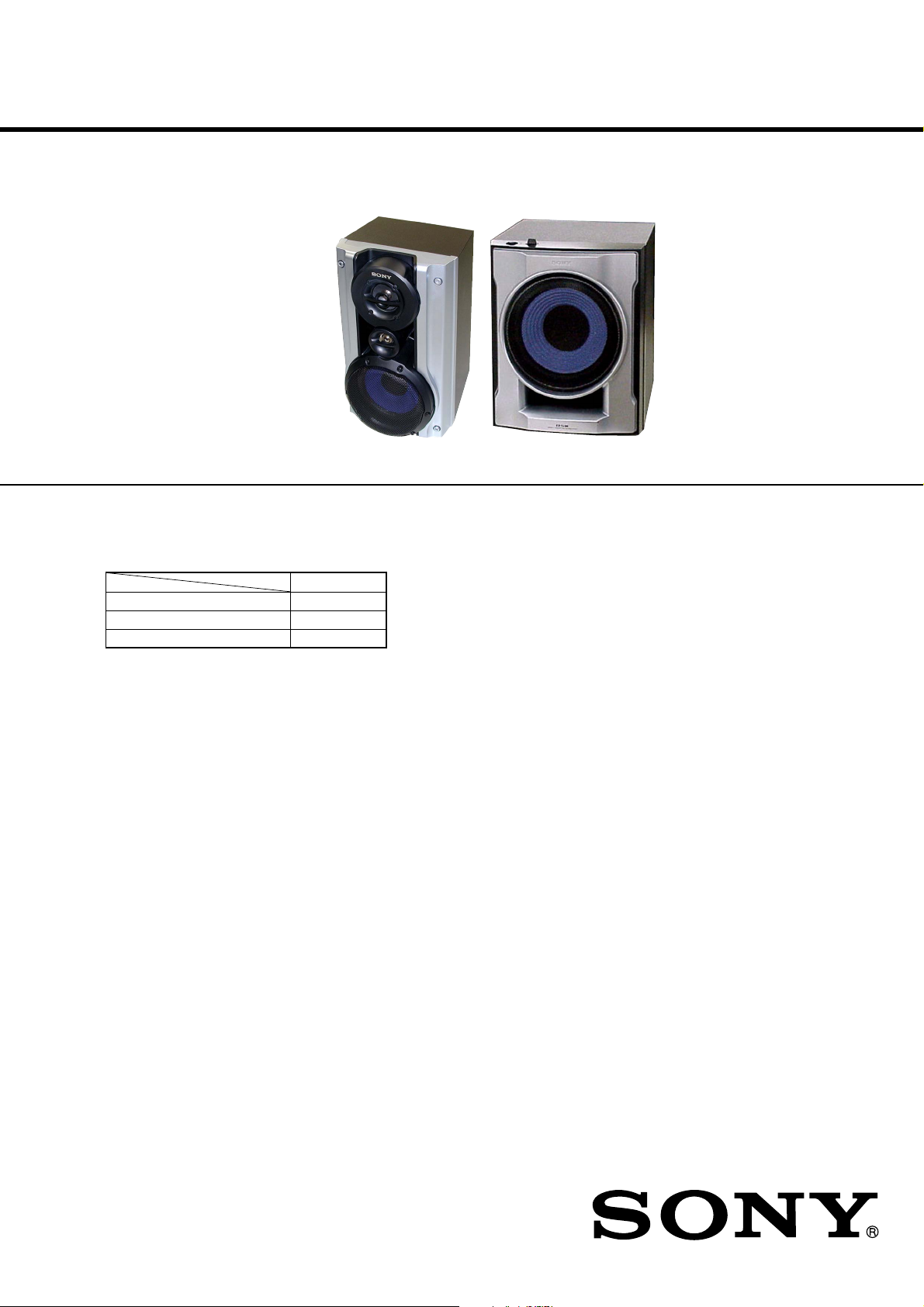
SS-RS999 SA-RV999D
• SA-RC999D is the speaker system in MHC-RV999D.
• SA-RC999D is composed of the following models.
COMPONENT MODEL NAME
SA-RC999D
SUB WOOFER SPEAKER SA-RV999D
SURROUND SPEAKER SS-RS999
CENTER SPEAKER SS-CT391
For the SS-CT391, refer to the respective service manual.
E Model
Australian Model
Surround speaker SS-RS999
Speaker system 3-way, 3-unit, bass-reflex
type
Speaker units
Super Tweeter: 2 cm, dome type
Woofer: 13 cm, cone type
Tweeter: 5 cm, cone type
Nominal impedance 6 ohms
Dimensions (w/h/d) Approx. 202 × 327 ×
230 mm
Mass Approx. 3.0 kg net per
speaker
SPECIFICATIONS
Sub woofer speaker SA-RV999D
Speaker system Active sub woofer,
magnetically shielded type
Speaker units 20 cm, cone type
Continuous RMS power output (reference)
120 watts
(6 ohms at 100 Hz, 10%
THD)
High frequency cut-off frequency
50 – 200 Hz
Phase selector NORMAL, REVERSE
Power consumption 100 watts
Dimensions (w/h/d) Approx. 270 × 325 ×
425 mm
Mass Approx. 10.0 kg net per
speaker
Design and specifications are subject to change
without notice.
SPEAKER SYSTEM
9-877-974-01
2004G04-1
© 2004. 07
Sony Corporation
Home Audio Company
Published by Sony Engineering Corporation
1

SA-RC999D/RV999D/SS-RS999
1. DIAGRAMS
1-1. Circuit Boards Location ...................................................... 3
1-2. Printed Wiring Boards – Except MX/TH/AUS Section – ...4
1-3. Schematic Diagram – Except MX/TH/AUS Section – ....... 5
1-4. Printed Wiring Boards – MX/TH/AUS Section – ............... 6
1-5. Schematic Diagram – MX/TH/AUS Section – ................... 7
2. EXPLODED VIEWS
2-1. Front Section (RV999D) ..................................................... 9
2-2. Rear Section (RV999D) .................................................... 10
2-3. Overall Section (SS-RS999) ............................................. 11
3. ELECTRICAL PARTS LIST ........................................ 12
TABLE OF CONTENTS
SAFETY-RELATED COMPONENT WARNING!!
COMPONENTS IDENTIFIED BY MARK 0 OR DOTTED LINE
WITH MARK 0 ON THE SCHEMATIC DIAGRAMS AND IN
THE PARTS LIST ARE CRITICAL TO SAFE OPERATION.
REPLACE THESE COMPONENTS WITH SONY P ARTS WHOSE
PART NUMBERS APPEAR AS SHOWN IN THIS MANUAL OR
IN SUPPLEMENTS PUBLISHED BY SONY.
2
SECTION 1
DIAGRAMS
SA-RC999D/RV999D/SS-RS999
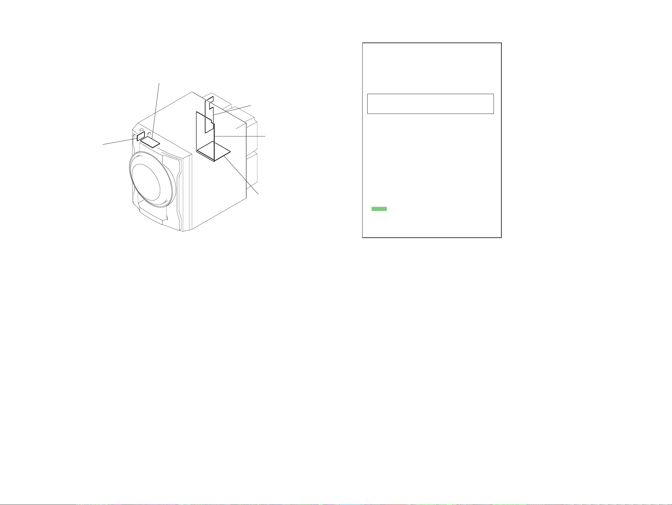
1-1. CIRCUIT BOARDS LOCATION
SWITCH board
CONTROL board
INPUT board
MAIN board
POWER board
Note on Schematic Diagram:
• All capacitors are in µF unless otherwise noted. (p: pF)
50 WV or less are not indicated except for electrolytics
and tantalums.
• All resistors are in Ω and 1/
specified.
• 2 : nonflammable resistor.
• C : panel designation.
Note: The components identified by mark 0 or dotted line
with mark 0 are critical for safety.
Replace only with part number specified.
• A : B+ Line.
• B : B– Line.
•Voltage is dc with respect to ground under no-signal
(detuned) condition.
•Voltages are taken with a VOM (Input impedance 10 MΩ).
Voltage variations may be noted due to normal production tolerances.
• Signal path.
F : AUDIO
• Abbreviation
MX : Mexican model
TH : Thai model
AUS : Australian model
Note on Printed Wiring Boards:
• X : parts extracted from the component side.
• : Pattern from the side which enables seeing.
• Abbreviation
MX : Mexican model
TH : Thai model
AUS : Australian model
4
W or less unless otherwise
SA-RC999D/RV999D/SS-RS999
33

SA-RC999D/RV999D/SS-RS999
1-2. PRINTED WIRING BOARDS — EXCEPT MX/TH/AUS SECTION — • Refer to page 3 for Circuit Boards Location. : Uses unleaded solder.
A
B
C
D
E
F
G
1
FH901
FH951
230-240V
220V
120V
VOLTAGE
SELECTOR
S1
F901
F903
2345678910111213
RV801
C203
CNP111
JW131
JW121
JW120
IC203IC202
R215
C801
C210
R217
G2
C211
C209
FH903
FH953
1
JW
JW2
C901
CN3
CN2
S901
SP1
CN1
JW401
G1
JW124
JW403
C401 C402
C403
R401
C405
JW123
JW125
CN402
D401
JW101
JW102
R403
C407
R402
FH902
C2
T1
CNP401
F902
FH952
D402
R506
C404
R404
C408
R500
C409
JW126
Q505
D403
D502
R507
CN301
C410
R313
D302C406
D301
JW404
JW402
R315
JW127
JW105
JW301
R501
JW103
JW104
R504
JW106
R309
JW501
D501
JW108
JW107
C303
R502
R311
JW110
JW128
C502
R503
C301
C302
C312
R303
Q502
JW109
R302
JW112
R505
JW111
R314
Q501
D304
R305
C311
C501
R508
RY301
C304
IC301
Q504
R312
R301
JW129
R304
C313
C305
Q503
R601
CN204
C503
D602
JW114
JW115
C306
D901
C205 C206
D205 D206
JW135
C310
R310
JW116
R307
C601
JW118
C309
C308
JW117
R306
CN202
JW132
JW119
C307
CN901
R209
R208
R207
CN201
JW122
C204
JW211
CNP801
R211
R210
JW133
JW134
R308
H
I
J
SA-RC999D/RV999D/SS-RS999
• Semiconductor Location
Ref. No. Location
D201 I-7
D202 I-7
D203 I-7
D204 I-7
D205 E-10
D206 E-10
D301 G-7
D302 G-7
D304 E-9
D401 D-6
D402 E-7
D403 D-7
D501 D-8
D502 G-7
Ref. No. Location
D602 D-9
D901 B-10
IC201 I-8
IC202 E-11
IC203 E-12
IC301 G-9
IC701 I-12
Q501 D-8
Q502 E-8
Q503 D-9
Q504 D-9
Q505 G-7
R109
44
R107
JW210
D201
D202
D204
D203
R108
JW208
TM101
R106
IC201
R203
R105
R103
JW204
R204
R104
R101
R102
JW206
CN101
R201
R110
C201
JW205
C702
C101
J101
C701
CN701
C704
RV701
JW209
JW207
R703
JW701
C705
JW702
R701
R704
R705
R708
R707
S701
C706
R706
IC701
R702
C703

1-3. SCHEMATIC DIAGRAM — EXCEPT MX/TH/AUS SECTION —
R102
R101
R104
TM101
J101
C101 R110
R108
R107
C201
R103
R105
R106
R109
R201
D201
D203
D202
D204
R203
IC201(1/2)
IC201(2/2)
R204
CN101 CN202
C701
C702
JW211
IC202(1/2)
R207
C203 C204
R210
R211
R208
R209
IC202(2/2)
D205
D206
C205
C206
CN201 CN701
R701
IC701(2/2)
R702
C703
R703
RV701
C704
R705 C705
R704
IC701(1/2)
R707
C706
SA-RC999D/RV999D/SS-RS999
S701
R708
R706
D901
CN901
CN204
C601
D602
Q505
D502
JW501
R506
R507
R601
R508
C503
Q504
Q503
R313
R315
R505
Q502
D301
D302
C502
R504
C301
IC301
C302R301
R302
R503 R502
Q501
R314
C501
R303
R309
C303
D501
C312
R312
C405
C406
R501 R500
F901
C801
RV801
SP1
CN3
CN2
C2
CN1
S901
C901
IC203(1/2)
R215
IC203(2/2)
R217 C211 C209
C313
R307R306
JW401
JW402
JW404
JW403
C305
C407
C408
R304
C307
C306
C403R401
C404
D402
D403
D401
C409
C410
C308
G1
R403
R404
C311R305
C304
R402
C309
C310
R310
R308
R311
D304
C401
C402
CN402
C210
RY301
T1
CNP401
CNP111 CNP801
CN301
JW1
S1
F903
JW2
F902
SA-RC999D/RV999D/SS-RS999
55
 Loading...