

Page 1
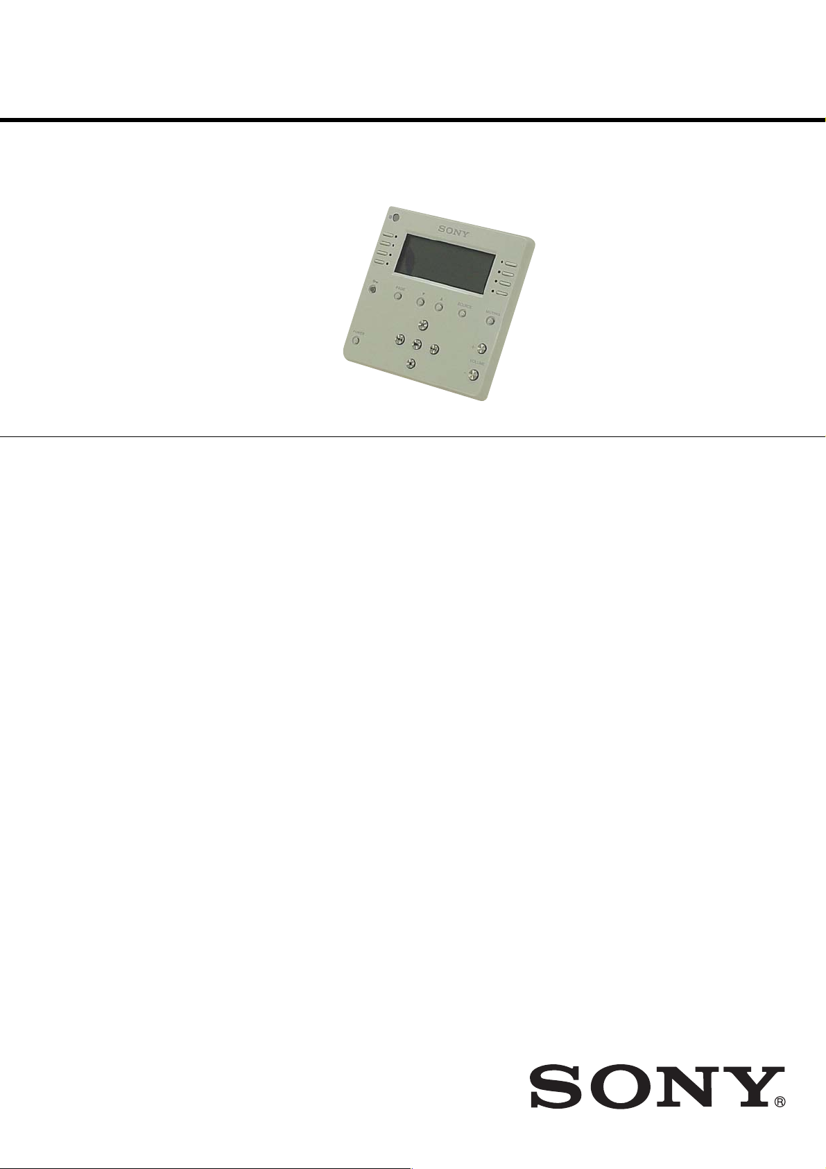
RMR-K100
SERVICE MANUAL
Ver 1.0 2004.05
SPECIFICATIONS
Operating system:Wired controller
LCD size:3 inches (80 ✕ 36 dots)
LCD type:Reflection system (mirror type)
Power requirements:
Connect to CAV-M1000ES via CAT5 cable
Maximum external dimensions:
125 ✕ 125 ✕ 53mm (5 ✕ 5 ✕ 2
(w/h/d, including projecting part and controls)
Mass: 240 g (8 oz)
Supplied accessories:
Bracket frame for KEYPAD attachment to a junction box
Screw B2 ✕ 8 for fixing KEYPAD to a Keypad mounting bracket (2)
Screw M3 ✕ 30 for Keypad mounting bracket fixing to a junction box (4)
RM-KP10 IR Remote Control for the Keypad
1
/8 inches)
US Model
9-877-895-01
2004E16-1
© 2004.05
Design and specifications are subject to change without notice.
KEYPAD
Sony Corporation
Home Audio Company
Published by Sony Engineering Corporation
Page 2

RMR-K100
Notes on chip component replacement
•Never reuse a disconnected chip component.
• Notice that the minus side of a tantalum capacitor may be
damaged by heat.
Flexible Circuit Board Repairing
•Keep the temperature of soldering iron around 270˚C during
repairing.
• Do not touch the soldering iron on the same conductor of the
circuit board (within 3 times).
• Be careful not to apply force on the conductor when soldering
or unsoldering.
UNLEADED SOLDER
Boards requiring use of unleaded solder are printed with the leadfree mark (LF) indicating the solder contains no lead.
(Caution: Some printed circuit boards may not come printed with
the lead free mark due to their particular size)
: LEAD FREE MARK
Unleaded solder has the following characteristics.
• Unleaded solder melts at a temperature about 40 °C higher
than ordinary solder.
Ordinary soldering irons can be used but the iron tip has to be
applied to the solder joint for a slightly longer time.
Soldering irons using a temperature regulator should be set to
about 350 °C.
Caution: The printed pattern (copper foil) may peel away if
the heated tip is applied for too long, so be careful!
• Strong viscosity
Unleaded solder is more viscou-s (sticky, less prone to flow)
than ordinary solder so use caution not to let solder bridges
occur such as on IC pins, etc.
• Usable with ordinary solder
It is best to use only unleaded solder but unleaded solder may
also be added to ordinary solder.
TABLE OF CONTENTS
1. GENERAL ................................................................... 3
2. DIAGRAMS
2-1. Block Diagram ................................................................ 6
2-2. Printed Wiring Board
– Front Display Board (Side A) –.................................... 7
2-3. Printed Wiring Board
– Front Display Board (Side B) –................................... 8
2-4. Schematic Diagram – Front Display Board – ................. 9
2-5. Printed Wiring Board – Bottom Supply Board – ............ 10
2-6. Schematic Diagram – Bottom Supply Board – ............... 11
3. EXPLODED VIEWS ................................................. 13
4. ELECTRICAL PARTS LIST .................................. 14
SAFETY-RELATED COMPONENT WARNING!!
COMPONENTS IDENTIFIED BY MARK 0 OR DOTTED LINE WITH
MARK 0 ON THE SCHEMATIC DIAGRAMS AND IN THE PARTS
LIST ARE CRITICAL TO SAFE OPERATION. REPLACE THESE
COMPONENTS WITH SONY PARTS WHOSE PART NUMBERS
APPEAR AS SHOWN IN THIS MANUAL OR IN SUPPLEMENTS
PUBLISHED BY SONY .
2
Page 3
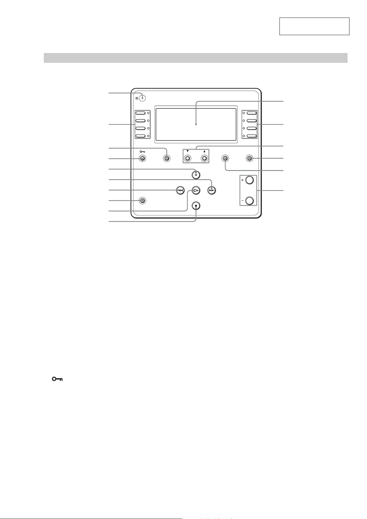
Front panel of the Keypad
1
SECTION 1
GENERAL
RMR-K100
This section is extracted
from instruction manual.
qa
2
3
PAGE SOURCE MUTING
4
5
6
7
POWER
8
9
0
1 IR sensor
Receives IR signals from the IR Remote Control for the
Keypad (supplied) to control both source components
and the system.
2 SELECT
Press to select a menu on the LCD display, such as a
source menu, a disc title list, etc.
The LED next to the SELECT button lights as follows
on the source selection:
–green: selected in the own zone
– amber: selected and locked in the other zone.
3 PAGE
Press to return to the previous menu or to view the
current status of the disc title list and the preset station
list. If there is no list, only a source name will be
displayed.
4
5 X (PAUSE)
(LOCK)
Press to lock the selected source.
– amber: locked
–off: released
Press to pause the playback.
2
qs
qd
qf
VOLUME
6 >
Press to advance the track/title or to select a preset
station.
7 .
Press to go reverse the track/title or to select a preset
station.
8 POWER switch
Press to turn the power of the Keypad on or off.
9 N (PLAY)
Press to operate the selected source.
0 x (STOP)
Press to stop playback.
qa Display window
Displays the selected source, the zone volume level,
the zone and the system status, and other system
status information.
qs v/V (SCROLL UP/DOWN)
Press to scroll the LCD menu.
qd MUTING
Press to mute the speaker output in the zone.
qf SOURCE
Press to return to the source components list screen.
qg
qg VOLUME +/–
Press to adjust the volume in a zone.
3
Page 4
RMR-K100
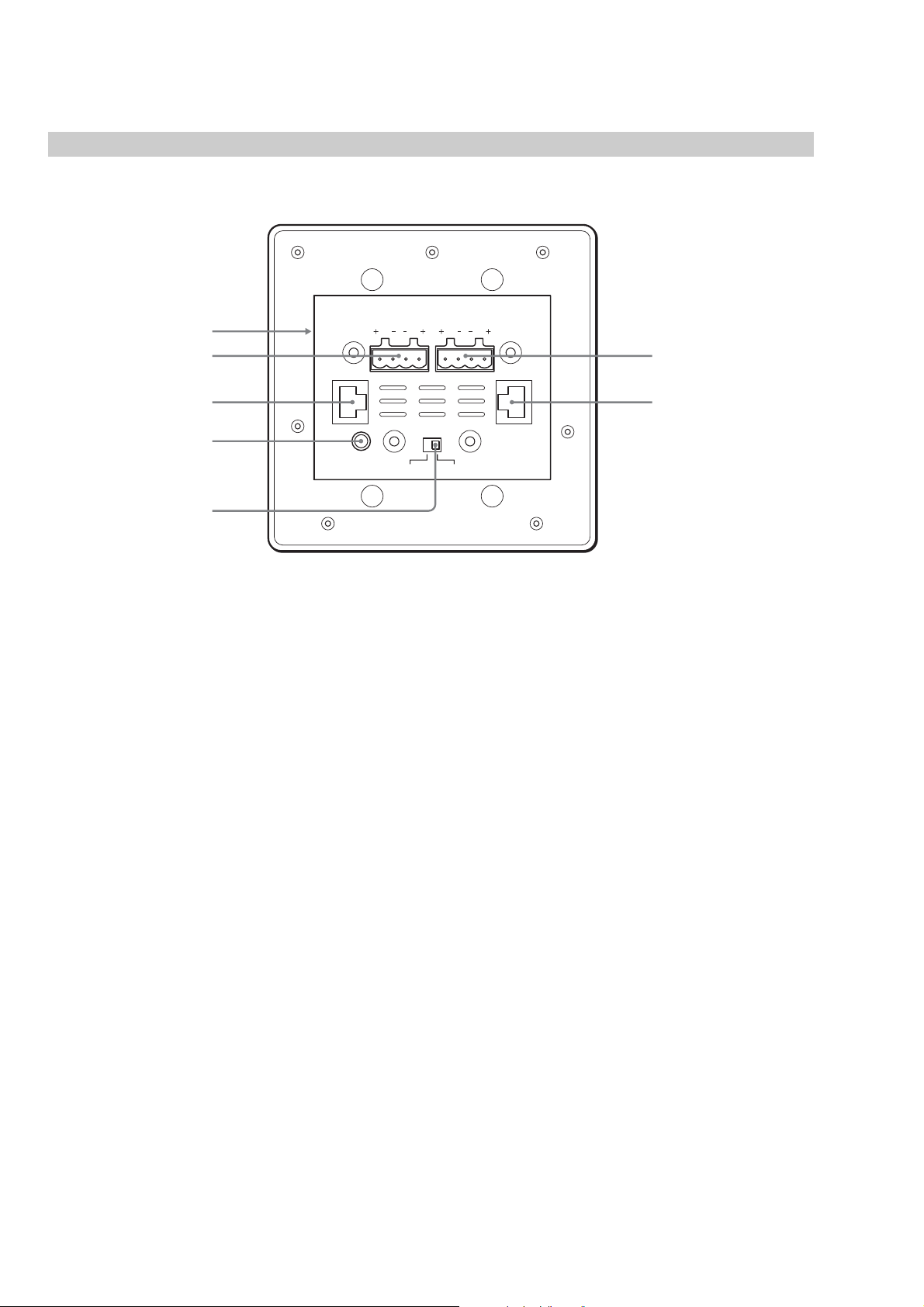
Rear panel of the Keypad
qh
OUT
ql
w;
qh Brightness adjustment hole (page 29)
The hole is located on the side.
Use a flathead screwdriver to adjust the brightness of
the background of the display window.
qj TO SPEAKERS (page 28)
Connects speaker cords to the speakers in a zone.
qk OUT (page 28)
Connects a CAT5 straight cable to the IN jack of the
subsidiary Keypad when used in a single room.
TO SPEAKERS
IR IN
FROM AMPLIFIER
L
R
L
R
waqj
IN
wsqk
MODE
MAIN
DC IN
SUB
ql IR IN (page 28)
Connects an optional IR emitter so you can operate the
IR Remote Control for the Keypad by pointing it at the
IR sensor of the connected IR emitter.
w; MODE switch (page 28)
When using two Keypads in a single room, set this
switch to SUB on the subsidiary Keypad.
wa FROM AMPLIFIER (page 28)
Connect speaker cords to the Main Unit.
ws IN (page 28)
Connects a CAT5 cable from the Main Unit to the main
Keypad.
4
Page 5
SECTION 2
d
1
IC300 is (XO)
62.5ns
3.0Vp-p
1V/DIV, 40ns/DIV
DIAGRAMS
RMR-K100
• Circuit Boards Location
FRONT DISPLAY board
COMM LEFT board
BOTTOM SUPPLY board
SPEAKER board
COMM RIGHT boar
Note on Schematic Diagram:
• All capacitors are in µF unless otherwise noted. (p: pF)
50 WV or less are not indicated except f or electrolytics and
tantalums.
• All resistors are in Ω and 1/
specified.
• C : panel designation.
• A : B+ Line.
•Power voltage is dc 12 V and fed with regulated dc power
supply from connector (CN500).
•Voltages and wavef orms are dc with respect to ground under no-signal (detuned) conditions.
no mark
•Voltages are taken with a VOM (Input impedance 10 MΩ).
•Waveforms are taken with a oscilloscope.
• Circled numbers refer to waveforms.
• Signal path.
: Power ON
Voltage variations may be noted due to normal production
tolerances.
Voltage variations may be noted due to normal production
tolerances.
F : AUDIO
4
W or less unless otherwise
•Waveform
Note on Printed Wiring Board:
• Y : parts extracted from the conductor side.
• : Pattern from the side which enables seeing.
Caution:
Pattern face side: Parts on the pattern face side seen from
(Side B) the pattern face are indicated.
Parts face side: Parts on the parts face side seen from
(Side A) the parts face are indicated.
• Indication of transistor.
C
These are omitted.
Q
B
E
RMR-K100
55
Page 6
RMR-K100
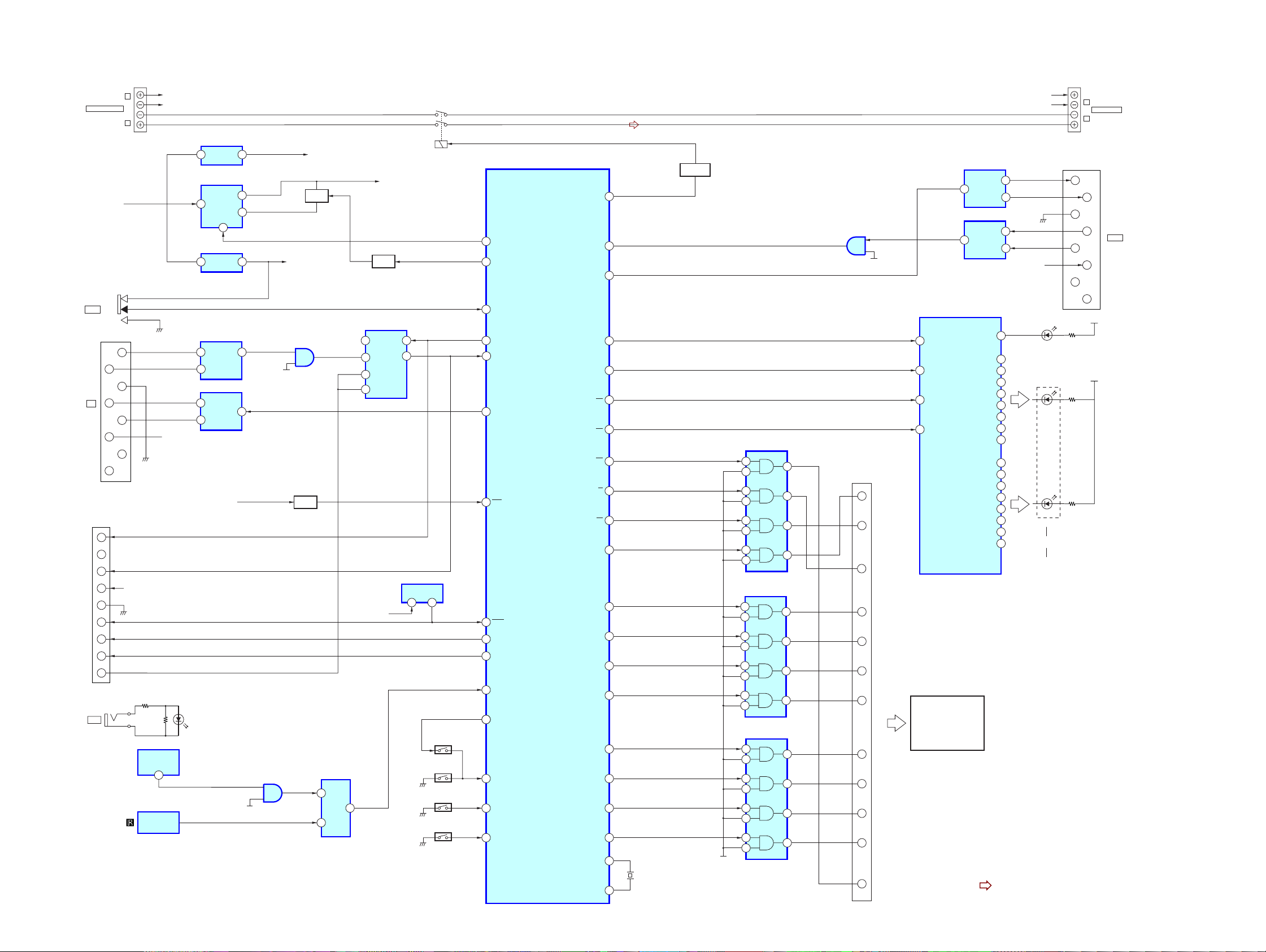
2-1. BLOCK DIAGRAM
FROM AMPLIFIFR
MAIN -
MODE
SUB -
IN
CN105
1
2
3
4
5
6
7
8
9
J600
IR IN
CN100
2
4
6
8
+12V
S300
1
3
5
7
FLASH1
FLASH2
+3.3V
RESET
MD0
MD2
CTL
CN107
R
L
RX+
RX-
IR RET
IR
R-CH
+12V
IC602
REMOTE CONTROLE
RECEIVER
1
IC601
REMOTE CONTROLE
RECEIVER
IC202
1 3
+5V REG
IC203 REG
VO
1
VIN
VADJ
VC
2
IC201
1 3
+3.3V REG
IC500
DIFFERENTIAL BUS TRANSCEIVER
6
RO
A
7
B
IC501
DIFFERENTIAL BUS TRANSCEIVER
7
B
D1
6
A
+12V
D600
CN108
R-CH
+5V
Q201
IC300
OFF
DIM2
SELECT
FLASH1
FLASH2
IR TX
STOP
RESET
MD0
MD2
SIRCS
POWER
AD0
AD1
AD2
SYSTEM CONTROLLER
SPK RELAY
IR RX
DATA
91
53
67
TX
17
16
CLK
15
STB
14
CLR
RES
13
CS
12
WR
10
9
OA
DB7
8
7
DB6
6
DB5
5
DB4
DB3
4
3
DB2
2
DB1
1
DB0
X0
82
X1
16MHz
83
XI
DC+12V
3.3V
11
+3.3V
IC404 (1/3)
1
2
BUFFER
Q200
SWITCH
Q202
SWITCH
3
MULTIPLEXER
7
6
IC600
ANALOG
CHO
CH1
COM
DUAL ANALOG SWITCH
6
2
3
7
1
O/I
O/I
COUNT
COUNT
Q203
SWITCH
IC302
+3.3V
88
87
89
5
I/O
1
I/O
IC301
RESET
12
S23
S1-S6, S14
S7-S13
S15-S21
28
27
68
48
77
49
51
52
456
38
39
40
3
4
1
4
IC404 (2/3)
BUFFER
13
12
3.3V
RELAY DRIVE
IC404 (3/3)
BUFFER
5
6
4
3.3V
SIRIAL PARALLEL CONVERTER
DATA
4
2
CLK
STB
30
CLB
31
IC402
BUFFER
9
10
1
2
5
4
13
12
9
10
5
4
1
2
13
12
9
10
5
4
1
2
13
12
+5V
IC401
BUFFER
IC400
BUFFER
8
CN106
3
6
11
8
6
3
11
8
6
3
11
1
2
3
4
5
6
7
8
9
10
11
23
LCD
IC503
DIFFERENTIAL BUS TRANSCEIVER
6
A
DI
4
DIFFERENTIAL BUS TRANSCEIVER
1
RO
IC100
7
B
IC504
7
B
6
A
11
P7
12
P8
14
P10
16
P12
18
P14
22
P18
24
P20
25
P21
27
P23
13
P9
15
P11
19
P15
17
P13
21
P17
23
P19
26
P22
28
P24
• R-CH is omitted due to same as L-CH.
• Signal Path
: AUDIO
+12V
IR RET
D103
D108
D112
D107
D105
R
TO SPEAKERS
L
CN500
TX+
1
TX-
2
3
4
IR
5
7
OUT
6
8
+5V
+5V
RMR-K100
66
Page 7

RMR-K100
2-2. PRINTED WIRING BOARD — FRONT DISPLAY BOARD (SIDE A) —
13
IC602
SELECT
SELECT
SELECT
• See page 5 for Circuit Boards Location. • :Uses unleaded solder.
SELECT
SELECT
SELECT
• Semiconductor
Location
Ref. No.
D103 E-2
D105 C-7
D106 C-7
D107 B-7
D108 B-2
D109 C-2
D110 C-2
D111 C-2
D112 B-2
D601 E-3
IC300 F-5
IC302 F-3
IC400 F-6
IC401 F-6
IC402 G-7
IC404 E-3
IC600 E-3
IC602 A-2
Location
SELECT
C314
IC404
PAGE
IC302
IC600
SELECT
SOURCE
IC400
R331
v
4
5
3
1
V
C801
X
IC301
R317
MUTING
IC401
C404
VOLUME +
RMR-K100
POWER
.
N
>
C423
IC402
VOLUME -
C419
x
77
Page 8

RMR-K100
2-3. PRINTED WIRING BOARD — FRONT DISPLAY BOARD (SIDE B) —
• See page 5 for Circuit Boards Location. • :Uses unleaded solder.
• Semiconductor
Location
Ref. No.
IC100 G-7
IC301 E-5
Location
COMM RIGHT
BOARD
(Page 10)
LIQUID
CRYSTAL
DISPLAY
COMM LEFT
BOARD
(Page 10)
IC300
RMR-K100
BOTTOM SUPPLY
BOARD
(Page 10)
IC100
BOTTOM SUPPLY
BOARD
(Page 10)
88
Page 9

RMR-K100
2-4. SCHEMATIC DIAGRAM — FRONT DISPLAY BOARD —
CN151
6P
CN103
10P
C
4
8
0
0
1
B
F
R803
47k
C801
4.7
C802
1
C803
1
R801
1M
C804
1
C805
1
C806
1
1
C807
C100
10
6.3V
R800
390k
C800
0.1
10
C808
FB800
4
2
C
C
4
E
S
6
0
1
D
0
9
3
9
1
1
R
3
8
5
0
4
0
8
2
1
1
C
D
C
E
E
S
S
3
0
1
D
0
0
0
6
3
6
5
3
5
6
8
0
1
1
1
R
R
k
5
7
0
4
1
3
0
R
0
1
3
1
2
3
1
R
R
• See page 12 for IC Block Diagrams.
X1
16MHz
G
2
T
Z
8
-G
C319
0.01
R394
1k
R395
1k
R396
100
R324
10k
R107
560
R117
390
R112
560
R116
390
R111
560
R110
560
R109
560
R114
390
R108
560
C430
47p
R325
100
R326
R327
100
R328
100
C401
0.01
IC100
BU2152FS
C101
C
M
N
C
1
9
0
2
3
9
IC
0
-8
S
C310
0.01
D107
R120
SEC2484C
390
D112
SEC2484C
D111
SEC2484C
D110
SEC2484C
R115
390
D109
SEC2484C
R113
D108
390
SEC2484C
C431
47p
0.1
C432C433
47p47p
• See page 5 for Waveform.
C610
0.1
IC404
TC74VHC08FT
C313
47p
C311
47p
C315
47p
R374
10k
.1
R331
0
10k
9
0
3
C
100
0
0
1
0
0
1
1
R300
100
R401
)
L
(E
T
F
A
8
0
T
C
H
V
4
7
C
T
0
0
4
IC
C400
47p
0
0
3
2
R
0
3
R
100
C402C403
47p47p
R400
100
C406
47p
0
0
0
0
0
0
0
0
0
1
1
1
1
1
4
7
3
5
6
0
0
0
0
0
3
3
3
3
3
R
R
R
R
R
C405
47p
R403
100
p
7
4
8
0
4
C
R402
100
C404
47p
C316
47p
R321
100
R311
R310
100
R309
100
C413
C409
47p
R404
C410
47p
IC300
MB90474HPF-GE1
100
R308
100
47p
C412
47p
R405
100
100
R362
R364
100
0
0
1
6
0
4
R
C314
47p
C318
100
R318
R721
10k
C300
0.01
C415
C418
47p
47p
R407
100
T
F
A
8
0
1
T
)
0
C
L
4
E
H
(
V
IC
4
7
C
T
p
7
C416
4
47p
7
1
C414
4
47p
C
C326
C312
10
0.01
6.3V
R392
100
47p
C317
47p
100
C320
0.1
R342
100
R313
R341
10k
100
C420C411
0.010.01
C419
47p
R607
10k
R317
10k
C422
R409
47p
100
C421
47p
1
k
0
.0
0
0
1
5
6
8
1
1
0
3
3
3
C
R
R
.1
0
R314
7
0
10k
3
C
k
0
1
2
1
7
R
C306
0.022
C305
0.022
C304
0.022
R704
C325
10k
R371
4.7k
R312
100k
C428
10
6.3V
C424
47p
R410
100
0
0
1
1
1
R408
4
100
R
C425
47p
C423
47p
0.1
0
0
3
B
F
C301
C302
10
0.01
6.3V
C321
R372
4.7k
T
F
A
8
0
2
T
0
C
4
H
IC
V
4
7
C
T
0.01
FB400
C426
47p
)
L
(E
p
7
4
7
2
4
C
S23 S3 S4 S5S6
IC600
TC7W53FU
10k
R720
S14
S7 S8 S9
C603
0.01
R713
22k
R706
22k
R714
22k
R705
10k
R707
10k
R715
10k
R606
100
C602
10
6.3V
R604
10
D601
ISS389
C601
2.2
16V
R605
100k
R603
100k
R601
10k
R373
100k
R375
100
R700
4.7k
S1
S2
R708
4.7k
S10 S11 S12 S13
R716
4.7k
IC602
PIC37041TM2
IC302
TC7W66FU
R701 R702
2.2k 2.2k
R709
2.2k
R717
2.2k
CN551
6P
CN503
10P
R370
100k
R376
100
C322
0.01
R703
1k
R710
2.2k
R718
2.2k
R711
1k
R719
1k
RMR-K100
CN106
S15 S16 S17 S18 S19
23P
S20 S21
99
Page 10

RMR-K100
2-5. PRINTED WIRING BOARD — BOTTOM SUPPLY BOARD —
• See page 5 for Circuit Boards Location. • :Uses unleaded solder.
IN
IC500
IC501
FRONT DISPLAY BOARD
(Page 8)
• Semiconductor
Location
Ref. No.
D201 K-11
D207 I-14
D600 K-8
D602 K-8
IC201 K-11
IC202 J-15
IC203 L-10
IC500 C-8
IC501 C-10
IC503 F-8
IC504 G-8
IC601 K-9
Q200 C-8
Q201 I-15
Q202 L-9
Q203 L-9
Location
IC503
IR IN
IC504
IC601
OUT
FRONT DISPLAY BOARD
MODE
(Page 8)
IC202
L
TO SPEAKERS
R
L
FROM AMPLIFIFIER
R
RMR-K100
not used
FRONT DISPLAY BOARD
(Page 8)
IC201
IC203
FRONT DISPLAY BOARD
(Page 8)
1010
Page 11

2-6. SCHEMATIC DIAGRAM — BOTTOM SUPPLY BOARD —
CN100
8P
C200
0.1
R201
4.7k
C202
1
50V
R202
1.5k
R203
2SC2712-YG-TE85L
R230
4.7k
10k
Q200
R501
100
C501
0.01
R500
10k
C500
10
16V
L500
R502
10k
X
M
C
0
5
0
8
5
4
S
IC
M
L
R518
10k
4
2
0
0
1
0
0
5
5
1
.0
R
C
0
X
M
C
1
5
0
8
5
4
S
IC
M
L
C508
47p
CN104
RMR-K100
CN108
4P
D207
1SR154-400TE-25
RY200
Q201
2SC3661-TB
CN154
10P
10P
R334
4.7k
FB201
C208
100
6.3V
IC202
C207
0.047
CN107
4P
CN555
10P
CN502
CN505
10P
C504
0.01
0
0
1
0
5
1
R
X
M
3
5C
0
8
5
4
S
IC
M
L
RV200
C510
47p
C507
10
16V
L501
10P
C505
0.01
3
0
1
0
5
1
R
X
M
4
5C
0
8
5
4
S
IC
M
L
CN501
9
k
1
0
5
1
R
R346
100
6P
CN500
8P
R343
100
CN101
6P
CN102
10P
IC601
NJL72H400A
IC203
CN152
10P
D201
CRS08-TE85R
C201
2200
25V
C205
0.047
C206
4700
5.5V
FB301
IC201
BA033T
S300
C204
47
0.047
6.3V
PQ20WZ5UJOOH
R225
1k
R216
C209
47k
R213
1k
R220
R210
82
1k
R211
1k
Q202
2SA1162-YG-TE85L
R212
R219
1k
1k
C218
4.7
35V
Q203
RT1N141C-TP-1
C216
C217
47
0.1
6.3V
C600
47
6.3V
D600
R600
R602
10
100
5
1
5
1
2
R
SID307BRTP19
CN105
9P
D602
R608
ISS355TE-17
10k
R610
10
CN552
10P
J600
RMR-K100
CN553CN153
10P10P
1111
Page 12

RMR-K100
• IC Block Diagrams
– FRONT DISPLAY BOARD –
IC302 TC7W66FU
VCC
CONT 1
OUT/IN 2
CONT 2
IN/OUT 2
GND
8 7 6 5
1
234
IN/OUT 1
OUT/IN 1
IC600 TC7W53FU
1
COM
2
INH
3
VEE
4
GND
LOGIC
LEVEL
CONVERTER
C
OUT
C
OUT IN
MEMO
VCC
8
CH 0
7
IN
CH 1
6
A
5
RMR-K100
1212
Page 13

NOTE:
d
• -XX and -X mean standardized parts, so they
may have some difference from the original
one.
SECTION 3
EXPLODED VIEWS
• The mechanical parts with no reference
number in the exploded views are not supplied.
not
supplied
308
not
supplied
RMR-K100
#1
#1
not
303
307
supplie
304
301
D800
306
305
304
302
Ref. No. Part No. Description Remark Ref. No. Part No. Description Remark
301 X-4955-988-1 FRONT PANEL ASSY
302 1-817-961-11 CONNECTOR
303 A-4749-507-A FRONT DISPLAY BOARD, COMPLETE
304 2-067-788-11 SCREW (B1.7), TAPPING
305 A-4749-509-A BOTTOM SUPPLY BOARD, COMPLETE
306 A-4749-513-A COMM RIGHT BOARD, COMPLETE
307 A-4749-515-A SPEAKER BOARD, COMPLETE
308 A-4749-511-A COMM LEFT BOARD, COMPLETE
D800 1-805-418-11 DISPLAY PANEL, LIQUID CRYSTAL
#1 7-685-646-79 SCREW +BVTP 3X8 TYPE2 IT-3
13
Page 14

RMR-K100
BOTTOM SUPPLY
COMM LEFT
NOTE:
• Due to standardization, replacements in the
parts list may be different from the parts
specified in the diagrams or the components
used on the set.
• -XX and -X mean standardized parts, so they
may have some difference from the original
one.
• Items marked “*” are not stocked since they
are seldom required for routine service.
Some delay should be anticipated when
ordering these items.
• CAPACITORS
uF: µF
Ref. No. Part No. Description Remark Ref. No. Part No. Description Remark
A-4749-509-A BOTTOM SUPPLY BOARD, COMPLETE
*******************************
7-685-646-79 SCREW +BVTP 3X8 TYPE2 IT-3
< CAPACITOR >
C201 1-126-943-11 ELECT 2200uF 20% 25V
C204 1-126-205-11 ELECT CHIP 47uF 20% 6.3V
C205 1-165-176-11 CERAMIC CHIP 0.047uF 10% 16V
C206 1-137-920-11 ELECT 4700uF 5.5V
C209 1-165-176-11 CERAMIC CHIP 0.047uF 10% 16V
C216 1-126-205-11 ELECT CHIP 47uF 20% 6.3V
C217 1-164-156-11 CERAMIC CHIP 0.1uF 25V
C218 1-126-603-11 ELECT CHIP 4.7uF 20% 35V
C600 1-126-205-11 ELECT CHIP 47uF 20% 6.3V
ELECTRICAL PARTS LIST
• RESISTORS
All resistors are in ohms.
METAL: Metal-film resistor.
METAL OXIDE: Metal Oxide-film resistor.
F: nonflammable
• COILS
uH: µH
• SEMICONDUCTORS
In each case, u: µ, for example:
uA. . : µA. . , uPA. . , µPA. .
uPB. . : µPB. . , uPC. . , µPC. .
uPD. . : µPD. .
SECTION 4
When indicating parts by reference number,
please include the board name.
< RESISTOR >
R210 1-216-821-11 METAL CHIP 1K 5% 1/10W
R211 1-216-821-11 METAL CHIP 1K 5% 1/10W
R212 1-216-821-11 METAL CHIP 1K 5% 1/10W
R213 1-216-821-11 METAL CHIP 1K 5% 1/10W
R215 1-215-858-00 METAL OXIDE 15 5% 1W
R216 1-216-841-11 METAL CHIP 47K 5% 1/10W
R219 1-216-821-11 METAL CHIP 1K 5% 1/10W
R220 1-216-808-11 METAL CHIP 82 5% 1/10W
R225 1-216-821-11 METAL CHIP 1K 5% 1/10W
R600 1-216-797-11 METAL CHIP 10 5% 1/10W
R602 1-216-809-11 METAL CHIP 100 5% 1/10W
R608 1-216-833-11 METAL CHIP 10K 5% 1/10W
R610 1-216-797-11 METAL CHIP 10 5% 1/10W
< CONNECTOR >
* CN105 1-565-980-11 HOUSING, CONNECTOR (PC BOARD) 9P
CN152 1-766-715-21 CONNECTOR, BOARD TO BOARD 10P
CN153 1-817-964-11 CONNECTOR (B TO B)
CN552 1-766-715-21 CONNECTOR, BOARD TO BOARD 10P
CN553 1-817-964-11 CONNECTOR (B TO B)
< DIODE >
D201 6-500-453-01 DIODE CRS08-TE85R
D600 8-719-075-86 DIODE SID307BRTP19
D602 8-719-988-61 DIODE 1SS355TE-17
< FERRITE BEAD >
FB301 1-414-813-11 FERRITE, EMI (SMD) (2012)
< IC >
IC201 8-759-445-59 IC BA033T
IC203 6-705-132-01 IC PQ20WZ5UJ00H
IC601 8-759-826-32 IC NJL72H400A
< JACK >
J600 1-563-330-11 JACK (IR IN)
< TRANSISTOR >
< SWITCH >
S300 1-762-175-11 SWITCH, SLIDE (MODE SUB/MAIN)
************************************************************
A-4749-511-A COMM LEFT BOARD, COMPLETE
**************************
< CAPACITOR >
C200 1-164-156-11 CERAMIC CHIP 0.1uF 25V
C202 1-126-193-11 ELECT CHIP 1uF 20% 50V
C500 1-124-779-00 ELECT CHIP 10uF 20% 16V
C501 1-162-970-11 CERAMIC CHIP 0.01uF 10% 25V
C502 1-162-970-11 CERAMIC CHIP 0.01uF 10% 25V
C508 1-162-923-11 CERAMIC CHIP 47PF 5% 50V
< CONNECTOR >
CN100 1-815-920-11 JACK, MODULAR (IN)
CN101 1-818-492-11 B TO B CONNECTOR
CN102 1-766-719-41 CONNECTOR, BOARD TO BOARD 10P
CN104 1-817-963-11 CONNECTOR (B TO B)
< IC >
IC500 6-705-128-01 IC LMS485CMX
IC501 6-705-128-01 IC LMS485CMX
Q202 8-729-216-22 TRANSISTOR 2SA1162-YG-TE85L
Q203 8-729-027-43 TRANSISTOR RT1N141C-TP-1
14
< COIL >
L500 1-414-813-11 FERRITE, EMI (SMD) (2012)
Page 15

RMR-K100
FRONT DISPLAYCOMM RIGHTCOMM LEFT
Ref. No. Part No. Description Remark Ref. No. Part No. Description Remark
< TRANSISTOR >
Q200 8-729-230-49 TRANSISTOR 2SC2712-YG-TE85L
< RESISTOR >
C304 1-164-227-11 CERAMIC CHIP 0.022uF 10% 25V
C305 1-164-227-11 CERAMIC CHIP 0.022uF 10% 25V
C306 1-164-227-11 CERAMIC CHIP 0.022uF 10% 25V
C307 1-107-826-11 CERAMIC CHIP 0.1uF 10% 16V
C308 1-162-970-11 CERAMIC CHIP 0.01uF 10% 25V
R201 1-216-829-11 METAL CHIP 4.7K 5% 1/10W
R202 1-216-823-11 METAL CHIP 1.5K 5% 1/10W
R203 1-216-833-11 METAL CHIP 10K 5% 1/10W
R230 1-216-829-11 METAL CHIP 4.7K 5% 1/10W
R343 1-216-809-11 METAL CHIP 100 5% 1/10W
R500 1-216-833-11 METAL CHIP 10K 5% 1/10W
R501 1-216-809-11 METAL CHIP 100 5% 1/10W
R502 1-216-833-11 METAL CHIP 10K 5% 1/10W
R504 1-216-809-11 METAL CHIP 100 5% 1/10W
R518 1-216-833-11 METAL CHIP 10K 5% 1/10W
************************************************************
A-4749-513-A COMM RIGHT BOARD, COMPLETE
****************************
< CAPACITOR >
C504 1-162-970-11 CERAMIC CHIP 0.01uF 10% 25V
C505 1-162-970-11 CERAMIC CHIP 0.01uF 10% 25V
C507 1-124-779-00 ELECT CHIP 10uF 20% 16V
C510 1-162-923-11 CERAMIC CHIP 47PF 5% 50V
< CONNECTOR >
CN500 1-815-920-11 JACK, MODULAR (OUT)
CN501 1-818-492-11 B TO B CONNECTOR
CN502 1-766-719-41 CONNECTOR, BOARD TO BOARD 10P
CN505 1-817-963-11 CONNECTOR (B TO B)
C309 1-107-826-11 CERAMIC CHIP 0.1uF 10% 16V
C310 1-162-970-11 CERAMIC CHIP 0.01uF 10% 25V
C311 1-162-923-11 CERAMIC CHIP 47PF 5% 50V
C312 1-162-970-11 CERAMIC CHIP 0.01uF 10% 25V
C313 1-162-923-11 CERAMIC CHIP 47PF 5% 50V
C314 1-162-923-11 CERAMIC CHIP 47PF 5% 50V
C315 1-162-923-11 CERAMIC CHIP 47PF 5% 50V
C316 1-162-923-11 CERAMIC CHIP 47PF 5% 50V
C317 1-162-923-11 CERAMIC CHIP 47PF 5% 50V
C318 1-162-923-11 CERAMIC CHIP 47PF 5% 50V
C319 1-162-970-11 CERAMIC CHIP 0.01uF 10% 25V
C320 1-107-826-11 CERAMIC CHIP 0.1uF 10% 16V
C321 1-162-970-11 CERAMIC CHIP 0.01uF 10% 25V
C322 1-162-970-11 CERAMIC CHIP 0.01uF 10% 25V
C325 1-107-826-11 CERAMIC CHIP 0.1uF 10% 16V
C326 1-127-692-11 CERAMIC CHIP 10uF 10% 6.3V
C400 1-162-923-11 CERAMIC CHIP 47PF 5% 50V
C401 1-162-970-11 CERAMIC CHIP 0.01uF 10% 25V
C402 1-162-923-11 CERAMIC CHIP 47PF 5% 50V
C403 1-162-923-11 CERAMIC CHIP 47PF 5% 50V
C404 1-162-923-11 CERAMIC CHIP 47PF 5% 50V
C405 1-162-923-11 CERAMIC CHIP 47PF 5% 50V
C406 1-162-923-11 CERAMIC CHIP 47PF 5% 50V
C408 1-162-923-11 CERAMIC CHIP 47PF 5% 50V
C409 1-162-923-11 CERAMIC CHIP 47PF 5% 50V
< IC >
IC503 6-705-128-01 IC LMS485CMX
IC504 6-705-128-01 IC LMS485CMX
< COIL >
L501 1-414-813-11 FERRITE, EMI (SMD) (2012)
< RESISTOR >
R346 1-216-809-11 METAL CHIP 100 5% 1/10W
R510 1-216-809-11 METAL CHIP 100 5% 1/10W
R513 1-216-809-11 METAL CHIP 100 5% 1/10W
R519 1-216-833-11 METAL CHIP 10K 5% 1/10W
< VARIABLE RESISTOR >
RV200 1-241-761-11
************************************************************
A-4749-507-A FRONT DISPLAY BOARD, COMPLETE
C100 1-127-692-11 CERAMIC CHIP 10uF 10% 6.3V
C101 1-107-826-11 CERAMIC CHIP 0.1uF 10% 16V
C300 1-162-970-11 CERAMIC CHIP 0.01uF 10% 25V
C301 1-127-692-11 CERAMIC CHIP 10uF 10% 6.3V
C302 1-162-970-11 CERAMIC CHIP 0.01uF 10% 25V
RES, ADJ, CARBON
******************************
< CAPACITOR >
1K
C410 1-162-923-11 CERAMIC CHIP 47PF 5% 50V
C411 1-162-970-11 CERAMIC CHIP 0.01uF 10% 25V
C412 1-162-923-11 CERAMIC CHIP 47PF 5% 50V
C413 1-162-923-11 CERAMIC CHIP 47PF 5% 50V
C414 1-162-923-11 CERAMIC CHIP 47PF 5% 50V
C415 1-162-923-11 CERAMIC CHIP 47PF 5% 50V
C416 1-162-923-11 CERAMIC CHIP 47PF 5% 50V
C417 1-162-923-11 CERAMIC CHIP 47PF 5% 50V
C418 1-162-923-11 CERAMIC CHIP 47PF 5% 50V
C419 1-162-923-11 CERAMIC CHIP 47PF 5% 50V
C420 1-162-970-11 CERAMIC CHIP 0.01uF 10% 25V
C421 1-162-923-11 CERAMIC CHIP 47PF 5% 50V
C422 1-162-923-11 CERAMIC CHIP 47PF 5% 50V
C423 1-162-923-11 CERAMIC CHIP 47PF 5% 50V
C424 1-162-923-11 CERAMIC CHIP 47PF 5% 50V
C425 1-162-923-11 CERAMIC CHIP 47PF 5% 50V
C426 1-162-923-11 CERAMIC CHIP 47PF 5% 50V
C427 1-162-923-11 CERAMIC CHIP 47PF 5% 50V
C428 1-127-692-11 CERAMIC CHIP 10uF 10% 6.3V
C430 1-162-923-11 CERAMIC CHIP 47PF 5% 50V
C431 1-162-923-11 CERAMIC CHIP 47PF 5% 50V
C432 1-162-923-11 CERAMIC CHIP 47PF 5% 50V
C433 1-162-923-11 CERAMIC CHIP 47PF 5% 50V
C601 1-164-505-11 CERAMIC CHIP 2.2uF 16V
C602 1-127-692-11 CERAMIC CHIP 10uF 10% 6.3V
C603 1-162-970-11 CERAMIC CHIP 0.01uF 10% 25V
C610 1-164-156-11 CERAMIC CHIP 0.1uF 25V
15
Page 16

RMR-K100
FRONT DISPLAY
Ref. No. Part No. Description Remark Ref. No. Part No. Description Remark
C800 1-107-826-11 CERAMIC CHIP 0.1uF 10% 16V
C801 1-127-820-11 CERAMIC CHIP 4.7uF 10% 16V
C802 1-165-908-11 CERAMIC CHIP 1uF 10% 10V
C803 1-165-908-11 CERAMIC CHIP 1uF 10% 10V
C804 1-165-908-11 CERAMIC CHIP 1uF 10% 10V
C805 1-165-908-11 CERAMIC CHIP 1uF 10% 10V
C806 1-165-908-11 CERAMIC CHIP 1uF 10% 10V
C807 1-165-908-11 CERAMIC CHIP 1uF 10% 10V
C808 1-127-692-11 CERAMIC CHIP 10uF 10% 6.3V
< CONNECTOR >
CN103 1-817-963-11 CONNECTOR (B TO B)
CN106 1-784-834-21 CONNECTOR, FFC (LIF (NON-ZIF)) 23P
CN151 1-818-491-11 B TO B CONNECTOR
CN503 1-817-963-11 CONNECTOR (B TO B)
CN551 1-818-491-11 B TO B CONNECTOR
< DIODE >
D103 8-719-064-55 DIODE SEC1803C
D105 8-719-064-56 DIODE SEC2484C
D106 8-719-064-56 DIODE SEC2484C
D107 8-719-064-56 DIODE SEC2484C
D108 8-719-064-56 DIODE SEC2484C
D109 8-719-064-56 DIODE SEC2484C
D110 8-719-064-56 DIODE SEC2484C
D111 8-719-064-56 DIODE SEC2484C
D112 8-719-064-56 DIODE SEC2484C
D601 8-719-083-15 DIODE 1SS389 (TPL3)
< FERRITE BEAD >
FB100 1-414-813-11 FERRITE, EMI (SMD) (2012)
FB300 1-414-813-11 FERRITE, EMI (SMD) (2012)
FB400 1-414-813-11 FERRITE, EMI (SMD) (2012)
FB800 1-414-813-11 FERRITE, EMI (SMD) (2012)
R110 1-216-818-11 METAL CHIP 560 5% 1/10W
R111 1-216-818-11 METAL CHIP 560 5% 1/10W
R112 1-216-818-11 METAL CHIP 560 5% 1/10W
R113 1-216-816-11 METAL CHIP 390 5% 1/10W
R114 1-216-816-11 METAL CHIP 390 5% 1/10W
R115 1-216-816-11 METAL CHIP 390 5% 1/10W
R116 1-216-816-11 METAL CHIP 390 5% 1/10W
R117 1-216-816-11 METAL CHIP 390 5% 1/10W
R118 1-216-816-11 METAL CHIP 390 5% 1/10W
R119 1-216-816-11 METAL CHIP 390 5% 1/10W
R120 1-216-816-11 METAL CHIP 390 5% 1/10W
R121 1-216-841-11 METAL CHIP 47K 5% 1/10W
R300 1-216-809-11 METAL CHIP 100 5% 1/10W
R301 1-216-809-11 METAL CHIP 100 5% 1/10W
R302 1-216-809-11 METAL CHIP 100 5% 1/10W
R303 1-216-809-11 METAL CHIP 100 5% 1/10W
R304 1-216-809-11 METAL CHIP 100 5% 1/10W
R305 1-216-809-11 METAL CHIP 100 5% 1/10W
R306 1-216-809-11 METAL CHIP 100 5% 1/10W
R307 1-216-809-11 METAL CHIP 100 5% 1/10W
R308 1-216-809-11 METAL CHIP 100 5% 1/10W
R309 1-216-809-11 METAL CHIP 100 5% 1/10W
R310 1-216-809-11 METAL CHIP 100 5% 1/10W
R311 1-216-809-11 METAL CHIP 100 5% 1/10W
R312 1-216-845-11 METAL CHIP 100K 5% 1/10W
R313 1-216-833-11 METAL CHIP 10K 5% 1/10W
R314 1-216-833-11 METAL CHIP 10K 5% 1/10W
R315 1-216-833-11 METAL CHIP 10K 5% 1/10W
R316 1-216-864-11 SHORT CHIP 0
R317 1-216-833-11 METAL CHIP 10K 5% 1/10W
R318 1-216-809-11 METAL CHIP 100 5% 1/10W
R321 1-216-809-11 METAL CHIP 100 5% 1/10W
R324 1-216-833-11 METAL CHIP 10K 5% 1/10W
R325 1-216-809-11 METAL CHIP 100 5% 1/10W
< IC >
IC100 6-701-888-01 IC BU2152FS
IC300 6-804-581-11 IC MB90474HPF-GE1
IC301 6-702-913-01 IC S-80929CNMC-G8ZT2G
IC302 8-759-488-29 IC TC7W66FU (TE12L)
IC400 8-759-491-47 IC TC74VHCT08AFT (EL)
IC401 8-759-491-47 IC TC74VHCT08AFT (EL)
IC402 8-759-491-47 IC TC74VHCT08AFT (EL)
IC404 8-759-523-81 IC TC74VHC08FT (EL)
IC600 8-759-564-49 IC TC7W53FU (TE12R)
IC602 6-600-287-01 IC PIC37041TM2 ( )
< SHORT >
JR100 1-216-296-11 SHORT CHIP 0
< RESISTOR >
R103 1-216-815-11 METAL CHIP 330 5% 1/10W
R105 1-216-818-11 METAL CHIP 560 5% 1/10W
R106 1-216-818-11 METAL CHIP 560 5% 1/10W
R107 1-216-818-11 METAL CHIP 560 5% 1/10W
R108 1-216-818-11 METAL CHIP 560 5% 1/10W
R109 1-216-818-11 METAL CHIP 560 5% 1/10W
R326 1-216-809-11 METAL CHIP 100 5% 1/10W
R327 1-216-809-11 METAL CHIP 100 5% 1/10W
R328 1-216-809-11 METAL CHIP 100 5% 1/10W
R331 1-216-833-11 METAL CHIP 10K 5% 1/10W
R341 1-216-809-11 METAL CHIP 100 5% 1/10W
R342 1-216-809-11 METAL CHIP 100 5% 1/10W
R362 1-216-809-11 METAL CHIP 100 5% 1/10W
R364 1-216-809-11 METAL CHIP 100 5% 1/10W
R370 1-216-845-11 METAL CHIP 100K 5% 1/10W
R371 1-216-829-11 METAL CHIP 4.7K 5% 1/10W
R372 1-216-829-11 METAL CHIP 4.7K 5% 1/10W
R373 1-216-845-11 METAL CHIP 100K 5% 1/10W
R374 1-216-833-11 METAL CHIP 10K 5% 1/10W
R375 1-216-809-11 METAL CHIP 100 5% 1/10W
R376 1-216-809-11 METAL CHIP 100 5% 1/10W
R392 1-216-809-11 METAL CHIP 100 5% 1/10W
R394 1-216-821-11 METAL CHIP 1K 5% 1/10W
R395 1-216-821-11 METAL CHIP 1K 5% 1/10W
R396 1-216-809-11 METAL CHIP 100 5% 1/10W
R400 1-216-809-11 METAL CHIP 100 5% 1/10W
R401 1-216-809-11 METAL CHIP 100 5% 1/10W
R402 1-216-809-11 METAL CHIP 100 5% 1/10W
R403 1-216-809-11 METAL CHIP 100 5% 1/10W
16
Page 17

RMR-K100
FRONT DISPLAY
Ref. No. Part No. Description Remark Ref. No. Part No. Description Remark
R404 1-216-809-11 METAL CHIP 100 5% 1/10W
R405 1-216-809-11 METAL CHIP 100 5% 1/10W
R406 1-216-809-11 METAL CHIP 100 5% 1/10W
R407 1-216-809-11 METAL CHIP 100 5% 1/10W
R408 1-216-809-11 METAL CHIP 100 5% 1/10W
R409 1-216-809-11 METAL CHIP 100 5% 1/10W
R410 1-216-809-11 METAL CHIP 100 5% 1/10W
R411 1-216-809-11 METAL CHIP 100 5% 1/10W
R601 1-216-833-11 METAL CHIP 10K 5% 1/10W
R603 1-216-845-11 METAL CHIP 100K 5% 1/10W
R604 1-216-797-11 METAL CHIP 10 5% 1/10W
R605 1-216-845-11 METAL CHIP 100K 5% 1/10W
R606 1-216-809-11 METAL CHIP 100 5% 1/10W
R607 1-216-833-11 METAL CHIP 10K 5% 1/10W
R700 1-216-829-11 METAL CHIP 4.7K 5% 1/10W
R701 1-216-825-11 METAL CHIP 2.2K 5% 1/10W
R702 1-216-825-11 METAL CHIP 2.2K 5% 1/10W
R703 1-216-821-11 METAL CHIP 1K 5% 1/10W
R704 1-216-833-11 METAL CHIP 10K 5% 1/10W
R705 1-216-833-11 METAL CHIP 10K 5% 1/10W
R706 1-216-837-11 METAL CHIP 22K 5% 1/10W
R707 1-216-833-11 METAL CHIP 10K 5% 1/10W
R708 1-216-829-11 METAL CHIP 4.7K 5% 1/10W
R709 1-216-825-11 METAL CHIP 2.2K 5% 1/10W
R710 1-216-825-11 METAL CHIP 2.2K 5% 1/10W
R711 1-216-821-11 METAL CHIP 1K 5% 1/10W
R712 1-216-833-11 METAL CHIP 10K 5% 1/10W
S16 1-762-333-21 SWITCH, TACTILE (>)
S17 1-762-333-21 SWITCH, TACTILE (x)
S18 1-762-333-21 SWITCH, TACTILE (-)
S19 1-762-333-21 SWITCH, TACTILE (MUTING)
S20 1-762-333-21 SWITCH, TACTILE (VOLUME +)
S21 1-762-333-21 SWITCH, TACTILE (VOLUME -)
S23 1-762-333-21 SWITCH, TACTILE (POWER)
< VIBRATOR >
X1 1-767-922-11 VIBRATOR, CERAMIC 16MHz
************************************************************
A-4749-515-A SPEAKER BOARD, COMPLETE
************************
7-685-646-79 SCREW +BVTP 3X8 TYPE2 IT-3
< CAPACITOR >
C207 1-165-176-11 CERAMIC CHIP 0.047uF 10% 16V
C208 1-126-206-11 ELECT CHIP 100uF 20% 6.3V
< CONNECTOR >
CN107 1-818-029-11 CONNECTOR PIN (FROM AMPLIFIER)
CN108 1-818-029-11 CONNECTOR PIN (TO SPEAKERS)
CN154 1-817-964-11 CONNECTOR (B TO B)
CN555 1-817-964-11 CONNECTOR (B TO B)
< DIODE >
SPEAKER
R713 1-216-837-11 METAL CHIP 22K 5% 1/10W
R714 1-216-837-11 METAL CHIP 22K 5% 1/10W
R715 1-216-833-11 METAL CHIP 10K 5% 1/10W
R716 1-216-829-11 METAL CHIP 4.7K 5% 1/10W
R717 1-216-825-11 METAL CHIP 2.2K 5% 1/10W
R718 1-216-825-11 METAL CHIP 2.2K 5% 1/10W
R719 1-216-821-11 METAL CHIP 1K 5% 1/10W
R720 1-216-833-11 METAL CHIP 10K 5% 1/10W
R721 1-216-833-11 METAL CHIP 10K 5% 1/10W
R800 1-216-852-11 METAL CHIP 390K 5% 1/10W
R801 1-216-857-11 METAL CHIP 1M 5% 1/10W
R803 1-216-841-11 METAL CHIP 47K 5% 1/10W
< SWITCH >
S1 1-762-333-21 SWITCH, TACTILE (SELECT)
S2 1-762-333-21 SWITCH, TACTILE (SELECT)
S3 1-762-333-21 SWITCH, TACTILE (SELECT)
S4 1-762-333-21 SWITCH, TACTILE (SELECT)
S5 1-762-333-21 SWITCH, TACTILE (SELECT)
S6 1-762-333-21 SWITCH, TACTILE (SELECT)
S7 1-762-333-21 SWITCH, TACTILE (SELECT)
S8 1-762-333-21 SWITCH, TACTILE (SELECT)
S9 1-762-333-21 SWITCH, TACTILE (SOURCE)
S10 1-762-333-21 SWITCH, TACTILE (V)
S11 1-762-333-21 SWITCH, TACTILE (v)
S12 1-762-333-21 SWITCH, TACTILE (PAGE)
S13 1-762-333-21 SWITCH, TACTILE (X)
S14 1-762-333-21 SWITCH, TACTILE (.)
S15 1-762-333-21 SWITCH, TACTILE (N)
D207 8-719-053-18 DIODE 1SR154-400TE-25
< FERRITE BEAD >
FB201 1-414-813-11 FERRITE, EMI (SMD) (2012)
< IC >
IC202 8-759-647-11 IC uPC2905HF
< TRANSISTOR >
Q201 8-729-802-80 TRANSISTOR 2SC3661-TB
< RESISTOR >
R334 1-216-829-11 METAL CHIP 4.7K 5% 1/10W
< RELAY >
RY200 1-755-518-11 RELAY
************************************************************
MISCELLANEOUS
**************
302 1-817-961-11 CONNECTOR
D800 1-805-418-11 DISPLAY PANEL, LIQUID CRYSTAL
************************************************************
ACCESSORIES
************
1-478-336-11 COMMANDER, STANDARD (RM-KP10)
4-253-729-11 INSTRUCTION MANUAL (KP) (ENGLISH)
17
Page 18

RMR-K100
REVISION HISTORY
Clicking the version allows you to jump to the revised page.
Also, clicking the version at the upper right on the revised page allows you to jump to the next revised
page.
Ver. Date Description of Revision
1.0 2004.05 New
 Loading...