Sony PRS-505 Service Manual
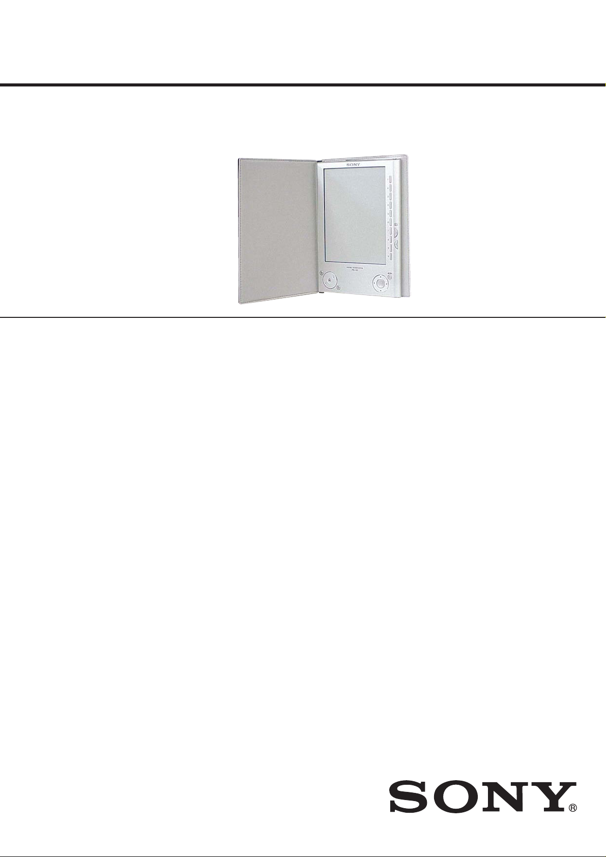
PRS-505
SERVICE MANUAL
Ver. 1.1 2007.12
• SONY and the SONY logo are registered trademarks of Sony Corporation.
• BBeB, BBeB Book, and their logos are trademarks of Sony Corporation.
• “Memory Stick,” “Memory Stick Duo,” “Memory Stick PRO Duo,” and their logos are trademarks of Sony Corporation.
• Bitstream is a registered trademark, and Dutch, Font Fusion, and Swiss are trademarks, of Bitstream Inc.
• Microsoft, Windows, W indows Vista and Windows Media are trademarks or registered trademarks of Microsoft Corporation
in the United States and / or other countries.
• Adobe, Adobe Reader and Adobe PDF are trademarks or registered trademarks of Adobe Systems Incorporated in the United
States and/or other countries.
• MPEG Layer-3 audio coding technology and patents licensed from Fraunhofer IIS and Thomson.Continued 90 US
• This product uses MontaVista Software, Inc.’s MontaVista(R) Linux(R) Professional Edition as the operating system.
COPYRIGHT ©1999-2006 MONTAVISTA SOFTWARE, INC. ALL RIGHTS RESERVED.
http://www.mvista.com/
• MontaVista is a registered trademark of MontaVista Software, Inc.
• This product includes software developed by the OpenSSL Project for use in the OpenSSL Toolkit. (<http://www.openssl.
org/>) Copyright © 1998-2006 The OpenSSL Project. All rights reserved. This product includes cryptographic software
written by Eric Young (eay@cryptsoft.com). This product includes software written by Tim Hudson (tjh@cryptsoft.com).
For details on OpenSSL License, refer to “openssl.txt” on the CD-ROM.
All other system names and product names appearing in this document are generally the registered trademarks or trademarks
of their respective manufacturers. Further, the trademark TM and registered trademark ® symbols are not indicated throughout
this document.
Program ©2006, 2007 Sony Corporation
Documentation ©2006, 2007 Sony Corporation
US Model
Canadian Model
SPECIFICATIONS
Power source
Built-in rechargeable battery: DC 3.7 V
AC power adapter: DC 5.2 V
Battery life (continuous playback)
Approx. 7500 pages (when the battery is fully charged)
User available capacity
Approx. 192MB
Available storage capacity of the Reader may vary.
Operating temperature
5 to 35 °C (41 to 95 °F)
Dimensions (w/h/d)
Approx. 6.9 × 4.8 × 0.3 inches (maximum, without soft cover)
Mass
Approx. 9 oz (without soft cover)
Package Contents
The Reader comes installed with a built-in rechargeable
battery.
• Reader (with Soft cover) (1)
• USB cable (1)
• CD-ROM (1)
- eBook Library software
- User’s Guide (PDF)
- Sample contents
• Quick Start Guide (this manual) (1)
• Flyers
• Dummy cards (2)
Note
• This CD-ROM will not play in an audio CD player.
9-887-835-02
2007L05-1
2007.12
©
Design and specifi cations are subject to change without notice.
PORTABLE READER SYSTEM
Sony Corporation
Audio Business Group
Published by Sony Techno Create Corporation

PRS-505
TABLE OF CONTENTS Notes on chip component replacement
1. SERVICING NOTES ............................................. 3
2. GENERAL .................................................................. 5
3. DISASSEMBLY
3-1. Disassembly Flow .......................................................... 6
3-2. Ornamental Plate (Upper) Assy, Plate (Case_Upper) .... 6
3-3. Ornamental Plate (Lower) Assy ...................................... 7
3-4. Main Assy ...................................................................... 7
3-5. (Ion) Storage Battery Assy ............................................. 8
3-6. SLOT FLEXIBLE Board ............................................... 8
3-7. CONNECT FLEXIBLE Board ...................................... 9
3-8. Frame ............................................................................. 9
3-9. MAIN Board, Ink (Indication) Element Assy (IIE1) ...... 10
4. TEST MODE ............................................................ 11
5. ELECTRICAL ADJUSTMENT ........................... 11
6. DIAGRAMS
6-1. Block Diagram - MAIN Section (1/2) - .......................... 12
6-2. Block Diagram - MAIN Section (2/2) - .......................... 13
6-3. Block Diagram - KEY/POWER SUPPLY Section - ....... 14
6-4. Printed Wiring Board
- MAIN Board (Component Side) - ................................ 16
6-5. Printed Wiring Board
- MAIN Board (Conductor Side) - .................................. 17
6-6. Schematic Diagram - MAIN Board (1/10) - ................... 18
6-7. Schematic Diagram - MAIN Board (2/10) - ................... 19
6-8. Schematic Diagram - MAIN Board (3/10) - ................... 20
6-9. Schematic Diagram - MAIN Board (4/10) - ................... 21
6-10. Schematic Diagram - MAIN Board (5/10) - ................... 22
6-11. Schematic Diagram - MAIN Board (6/10) - ................... 23
6-12. Schematic Diagram - MAIN Board (7/10) - ................... 24
6-13. Schematic Diagram - MAIN Board (8/10) - ................... 25
6-14. Schematic Diagram - MAIN Board (9/10) - ................... 26
6-15. Schematic Diagram - MAIN Board (10/10) - ................. 27
6-16. Printed Wiring Board
- CONNECT FLEXIBLE Board - .................................. 28
6-17. Schematic Diagram
- CONNECT FLEXIBLE Board - .................................. 28
• Never reuse a disconnected chip component.
• Notice that the minus side of a tantalum capacitor may be damaged by heat.
Flexible Circuit Board Repairing
• Keep the temperature of soldering iron around 270 °C during
repairing.
• Do not touch the soldering iron on the same conductor of the
circuit board (within 3 times).
• Be careful not to apply force on the conductor when soldering
or unsoldering.
CAUTION
Danger of explosion if battery is incorrectly replaced. Replace only with
the same or equivalent type.
7. EXPLODED VIEWS
7-1. Case Section ................................................................... 44
7-2. Main Section .................................................................. 45
8. ELECTRICAL PARTS LIST .............................. 46
2
SAFETY-RELATED COMPONET WARNING!
COMPONENTS IDENTIFIED BY MARK 0 OR DOTTED LINE
WITH MARK 0 ON THE SCHEMATIC DIAGRAMS AND IN
THE PARTS LIST ARE CRITICAL TO SAFE OPERATION.
REPLACE THESE COMPONENTS WITH SONY PARTS
WHOSE PART NUMBERS APPEAR AS SHOWN IN THIS
MANUAL OR IN SUPPLEMENTS PUBLISHED BY SONY.
ATTENTION AU COMPOSANT AYANT RAPPORT
À LA SÉCURITÉ!
LES COMPOSANTS IDENTIFIÉS PAR UNE MARQUE 0 SUR
LES DIAGRAMMES SCHÉMATIQUES ET LA LISTE DES
PIÈCES SONT CRITIQUES POUR LA SÉCURITÉ DE FONCTIONNEMENT. NE REMPLACER CES COM- POSANTS QUE
PAR DES PIÈCES SONY DONT LES NUMÉROS SONT DONNÉS DANS CE MANUEL OU DANS LES SUPPLÉMENTS
PUBLIÉS PAR SONY.
SECTION 1
SERVICING NOTES
PRS-505
UNLEADED SOLDER
Boards requiring use of unleaded solder are printed with the leadfree mark (LF) indicating the solder contains no lead.
(Caution: Some printed circuit boards may not come printed with
the lead free mark due to their particular size)
: LEAD FREE MARK
Unleaded solder has the following characteristics.
• Unleaded solder melts at a temperature about 40 °C higher
than ordinary solder.
Ordinary soldering irons can be used but the iron tip has to be
applied to the solder joint for a slightly longer time.
Soldering irons using a temperature regulator should be set to
about 350 °C.
Caution: The printed pattern (copper foil) may peel away if the
heated tip is applied for too long, so be careful!
• Strong viscosity
Unleaded solder is more viscous (sticky, less prone to fl ow)
than ordinary solder so use caution not to let solder bridges
occur such as on IC pins, etc.
• Usable with ordinary solder
It is best to use only unleaded solder but unleaded solder may
also be added to ordinary solder.
REWRITING THE LUT
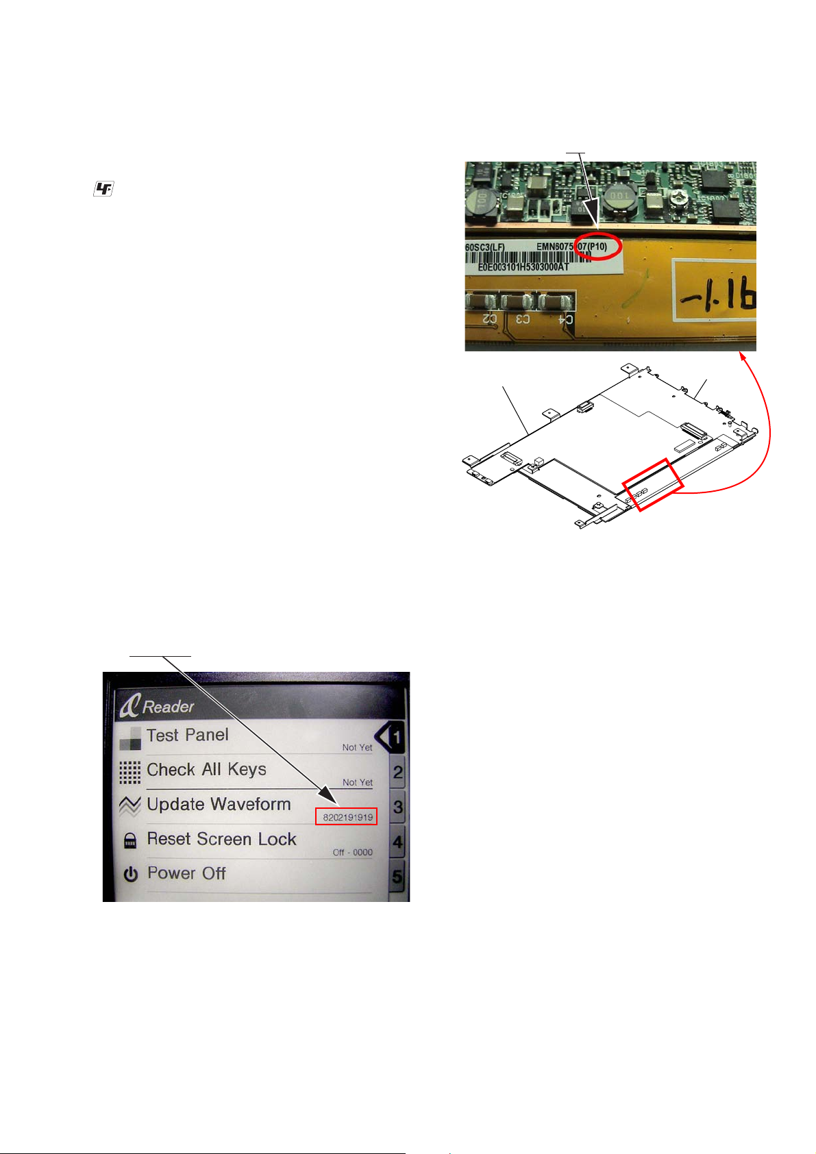
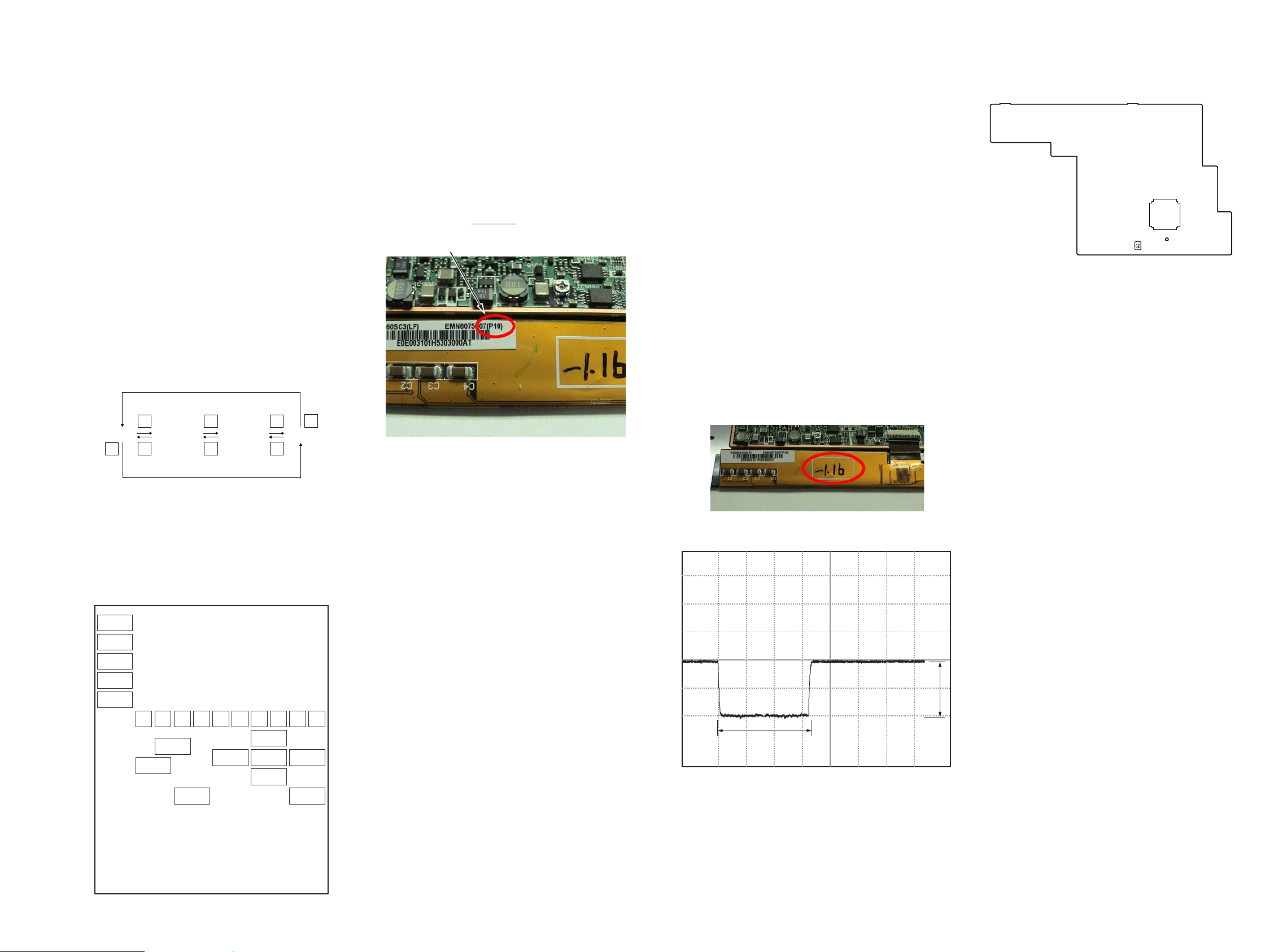
The LUT is exclusive for each lot number of the INK INDICATOR
ELEMENT ASSY. Therefore, when replacing the MAIN board,
display panel, or FLASH ROM, you need to rewrite the LUT.
However, rewriting is not required if the lot number is the same.
How to check the lot number of the ink (indication)
ELEMENT ASSY :
• The lot number is written on the label on the fl exible card wire.
The lot number is “P10” in the picture below.
ink (indication)
main board
element assy
Location where the LUT is stored:
• IC1203
How to check the version of the stored LUT:
• When you insert the memory stick or SD memory card in
which the exclusive fi le is stored, the test mode is established.
Check the current LUT version displayed at the right side of
“Update Waveform” as in the screen below. The LUT version
is “8202191919” in this example.
(Screen display)
How to change the LUT:
• Copy the LUT fi le you want to update to the folder under “/
Sony Reader/software” in the memory stick or SD memory
card exclusive for the test mode, and then change the name to
“lut.bin”. Execute test mode No.3 “Update Waveform”. The
LUT will be updated in about 10 seconds, and the LUT version
display will also change.
• For the LUT version and the LUT fi le corresponding to the lot
number of the panel, refer to technical news.
Note:
• To create the memory stick exclusive for the test mode, refer to TEST
MODE (Page 11).
• For the VCOM adjustment value of RV1801 for each lot, refer to
ELECTRICAL ADJUSTMENT (Page 11).
3

PRS-505
NOTE THE IC1001 ON THE MAIN BOARD
REPLACING
Replacement of IC1001 on the MAIN board used in this set requires a special tool
NOTE THE IC301, IC953, IC1106, IC1201, IC1202 AND
IC1203 ON THE MAIN BOARD REPLACING
When IC301, IC953, IC1106, IC1201, IC1202 and IC1203 on the
MAIN board is damaged, exchange the new MAIN board for the
MAIN board which IC damaged
NOTES WHEN REPLACING THE INK INDICATOR
ELEMENT ASSY, MAIN BOARD AND FLASH ROM
(IC1203)
When the INK INDICATOR ELEMENT ASSY, MAIN board, or
FLASH ROM (IC1203) is replaced, you need to change the LUT.
REMOVING/ATTACHING THE SOFT COVER
"
• Removing the soft cover
Pull the tab of soft cover towards " .
Remove Sony’s Reader in the direction of # .
• Attaching the soft cover
Insert the tab $ of the soft cover in the hole % of Sony’s
Reader.
Pull the tab of the soft cover towards " .
Insert Sony’s Reader in the direction of & to attach it to the soft
cover.
Check that the tabs of the soft cover are completely inserted in
the holes of Sony’s Reader.
#
&
%$
Note: Note that the tab of the soft cover may become deformed,
if you strongly pull the tab too much.
4
SECTION 2
GENERAL
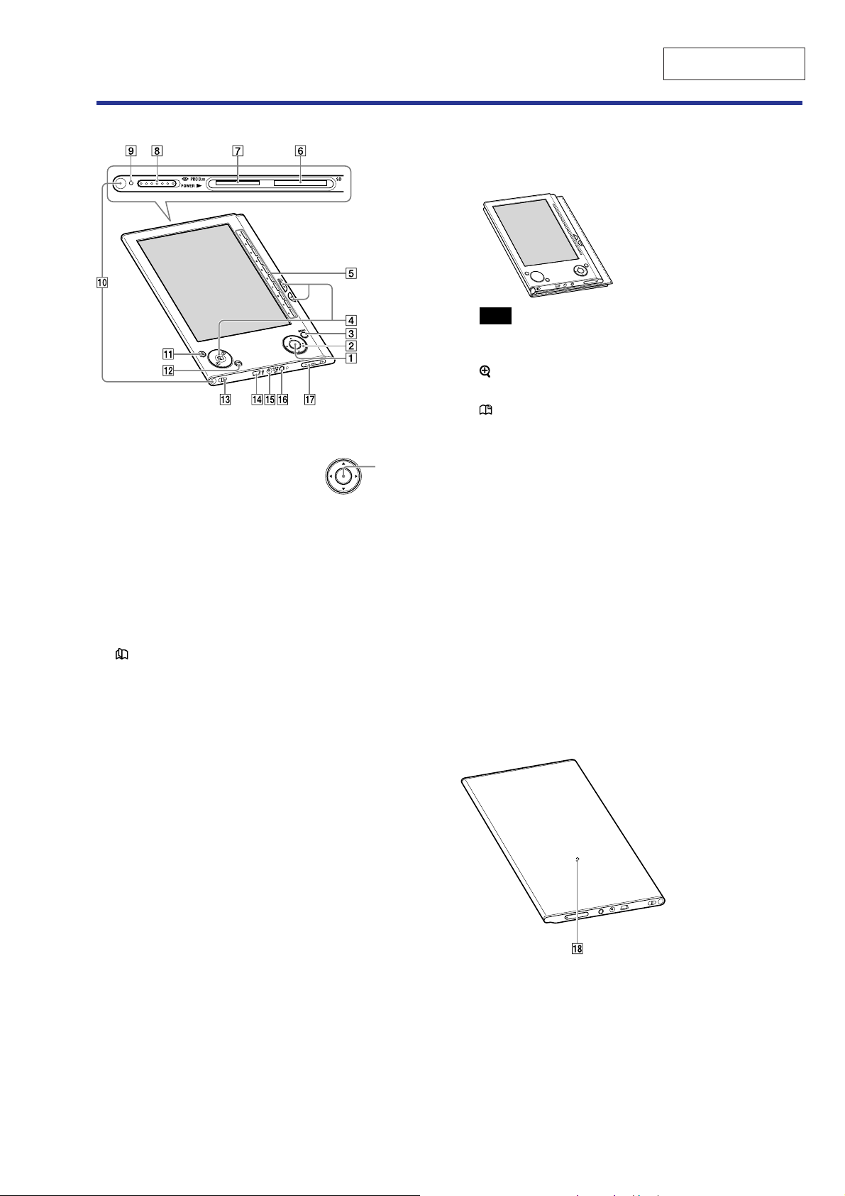
Guide to Parts and Controls
Front
Enter button*
To decide an item or apply a
setting, press the Enter button.
/// buttons*
To select an item or scroll around the screen, press
(left), (up), (down), or (right).
*1In this manual, the operation of the ////Enter buttons are
explained as follows.
(Example) Press /// to select “Away” on the Book list, then
press Enter.
MENU button
To return to the previous screen or show a menu.
(page) / (>/<) buttons
To turn the page or proceed/return to the next (>)/
previous (<) content.
Number (1 – 9,0) buttons
To select the numbered items on the screen or input
numeric values on the Setting menu.
SD Memory Card slot
To insert a SD Memory Card (optional).
“Memory Stick Duo” slot
To insert a “Memory Stick Duo” (optional).
POWER switch
To switch on/off the Reader.
Indicator
Lights up in red while charging, and goes off when
charging is complete.
Flashes in orange while the Reader is accessing your
computer via USB.
Also flashes in orange while switching the Reader on
or off.
1
Enter button
1
PRS-505
This section is extracted
from instruction manual.
Holes for soft cover attachment
The soft cover is attached when purchased.
Folds open in use
1
2
3
4
5
6
7
8
9
0
Note
• Do not leave the Reader in a high temperature conditions,
as it may damage the soft cover.
(size) button
To zoom in/out a page or picture.
(MARK) button
To create/remove a bookmark.
Hole for hand strap
To attach the hand strap.
USB connector
To connect the USB cable (supplied).
DC IN jack
To connect the AC power adapter (optional).
Hint
• The Reader can be charged by connecting to a computer
using the supplied USB cable.
(Headphones) jack
To connect headphones (optional).
VOLUME +/– buttons
To adjust the volume.
To mute the sound, press and hold the VOLUME +/–
buttons.To restore the sound, press the VOLUME +/–
buttons again.
Rear
Reset button
To reset the Reader if no operation is possible.
5
PRS-505
SECTION 3
DISASSEMBLY
• This set can be disassembled in the order shown below.
3-1. DISASSEMBLY FLOW
Note 1: The process described in can be performed in any order.
Note 2: Without completing the process described in , the next process can not be performed.
Note 3: Please refer to SERVICING NOTES “REMOVING/ATTACHING THE SOFT COVER” (page 4).
SET
3-2. ORNAMENTAL PLATE (UPPER) ASSY,
PLATE (CASE-UPPER)
(Page 6)
3-4. MAIN ASSY
(Page 7)
3-5. (ION) STORAGE
BATTERY ASSY
(Page 8)
3-8. FRAME
(Page 9)
3-9. MAIN BOARD, INK (INDICATION) ELEMENT ASSY (IIE1)
(Page 10)
3-6. SLOT FLEXIBLE
BOARD
(Page 8)
3-3. ORNAMENTAL PLATE
(LOWER) ASSY
(Page 7)
3-7. CONNECT FLEXIBLE
BOARD
(Page 9)
Note: Follow the disassembly procedure in the numerical order shown below.
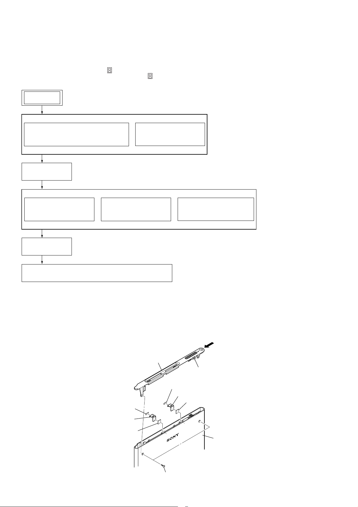
3-2. ORNAMENTAL PLATE (UPPER) ASSY, PLATE (CASE_UPPER)
Note: When peeling off adhesive sheet,
be sure to exchange it for new adhesive sheet.
Remove while moving ornamental plate (upper) assy
in the direction of the arrow.
claw
adhesive sheet (C)
plate (case_upper)
adhesive sheet (B)
adhesive sheet (C)
plate (case_upper)
adhesive sheet (B)
two screws (M1.4)
The upper part of the back side
6
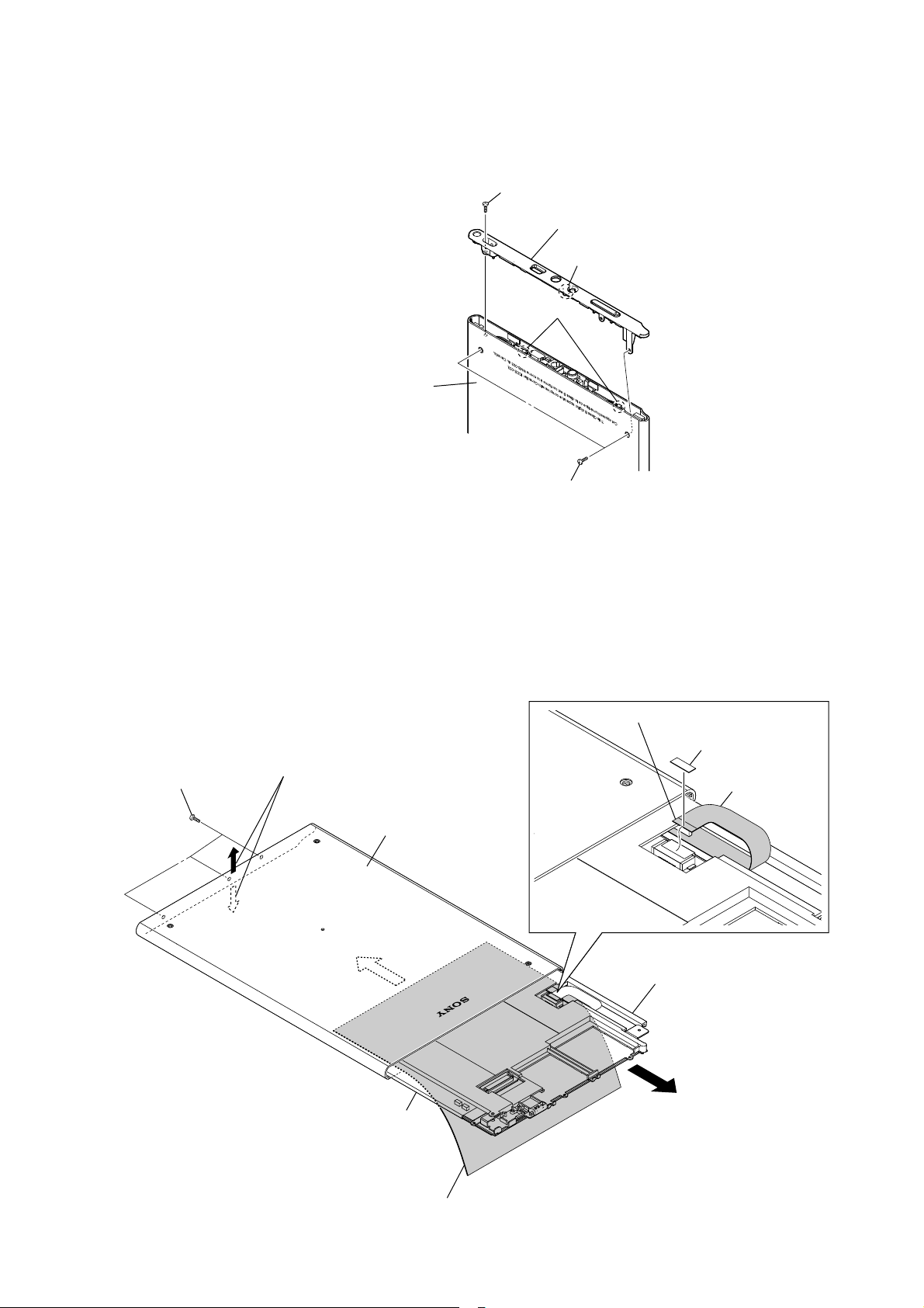
3-3. ORNAMENTAL PLATE (LOWER) ASSY
The lower part of the back side
PRS-505
screw (M1.4)
ornamental plate (lower) assy
claw
two claws
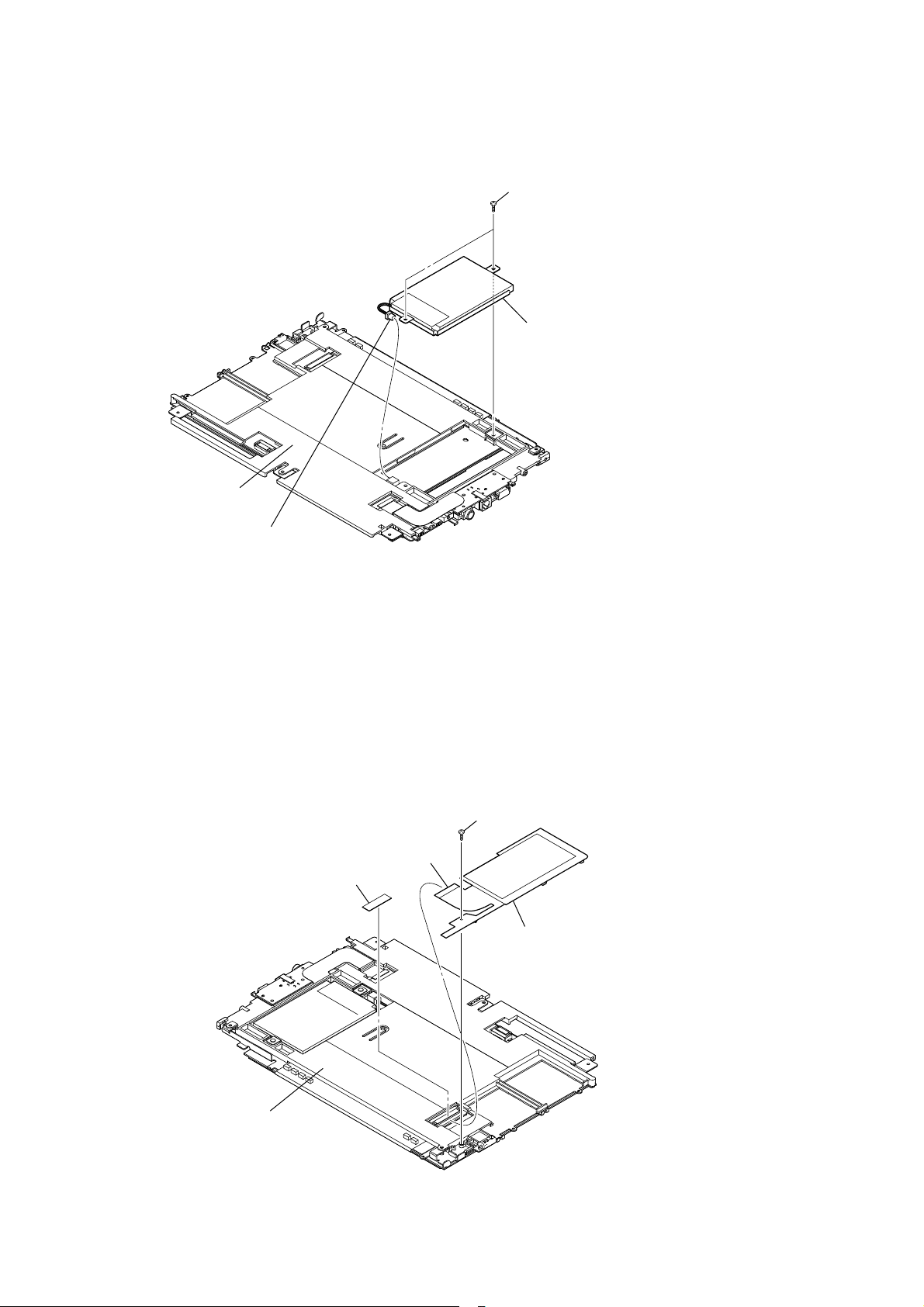
3-4. MAIN ASSY
three tapping screws
Please open the lower side of case assy
a little up and down.
case assy
back side
two screws (M1.4)
connector (CN801)
spacer (CON_key)
KEY FLEXIBLE board
Please draw out main assy to the half
noting that KEY FLEXIBLE board does not stretch
in the direction of the arrow.
Please insert paper and the film, etc.
in the space of case assy not to be damaged
of the display side of INK(indikation) element assy.
Please draw out main assy
from case assy in the direction
of the arrow completely
after removing the connector (CN801).
7
PRS-505
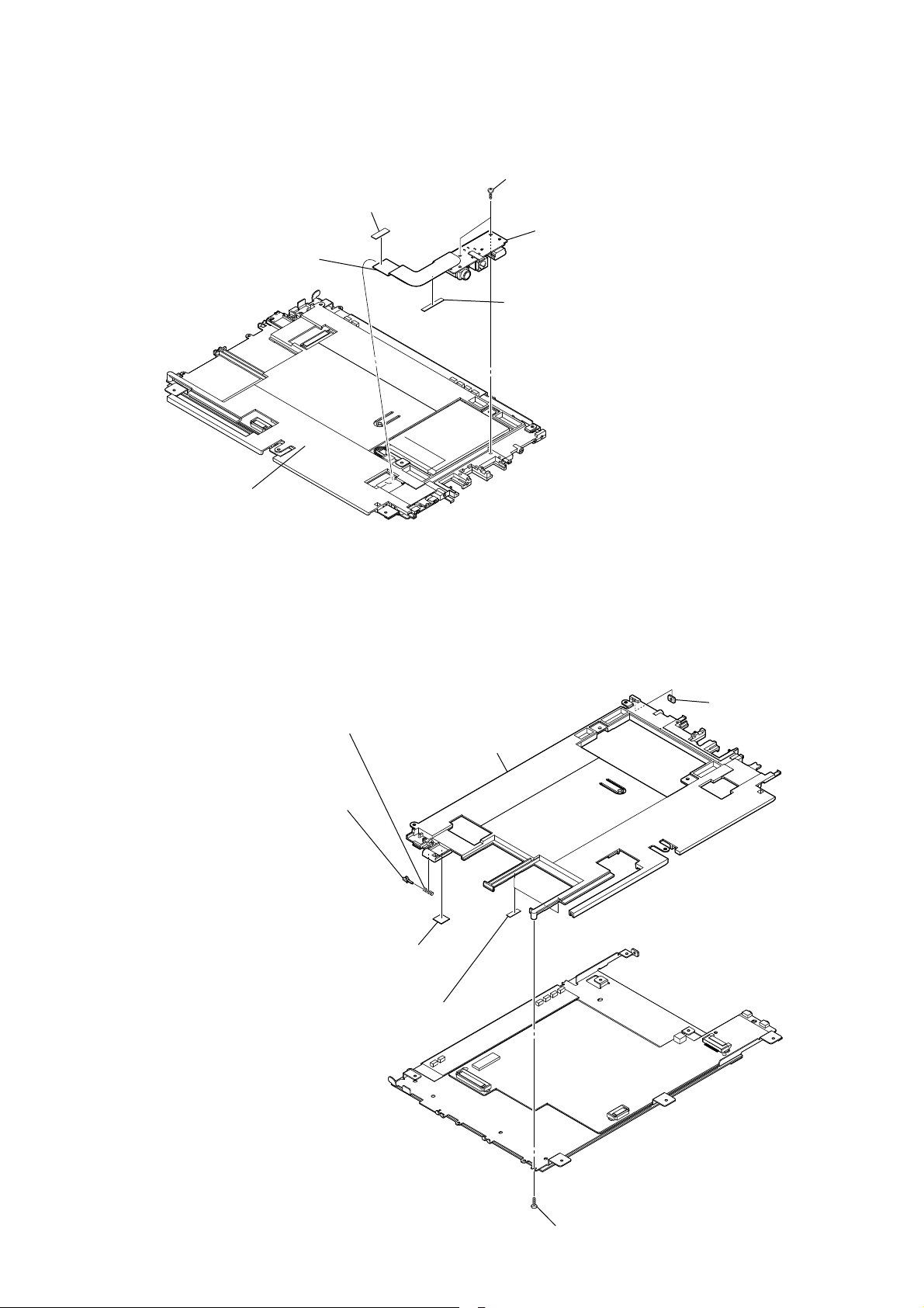
3-5. (ION) STORAGE BATTERY ASSY
two screws (M1.4)
upper side
main assy
back side
connector (CN401)
3-6. SLOT FLEXIBLE BOARD
(ion) storage battery assy
lower side
spacer (CON_SD)
lower side
main assy
back side
two screws (M1.4)
connector
(CN201)
SLOT FLEXIBLE board
upper side
8
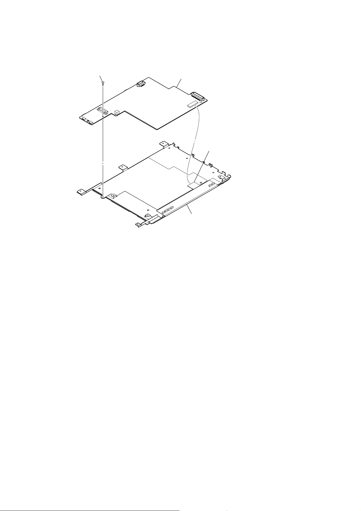
3-7. CONNECT FLEXIBLE BOARD
spacer (CON_USB)
connector (CN901)
upper side
PRS-505
two screws (M1.4)
CONNECT FLEXIBLE board
adhesive sheet (D)
Note: When peeling off adhesive sheet,
be sure to exchange it for new adhesive sheet.
main assy
back side
3-8. FRAME
compression spring
Note: Note the loss
because it is likely to dash out
when it removes.
shaft (spring)
Note: Note the loss
because it is likely to dash out
when it removes.
adhesive sheet (A)
Note: When peeling off adhesive sheet,
be sure to exchange it for new adhesive sheet.
lower side
nut plate
Note: Note the loss.
frame
two adhesive sheets (B)
Note: When peeling off adhesive sheet,
be sure to exchange it for new adhesive sheet.
screw (M1.4)
9
PRS-505
3-9. MAIN BOARD, INK (INDICATION) ELEMENT ASSY (IIE1)
screw (M1.4 × 2)
MAIN board
connector (CN302)
ink (indication) element assy (IIE1)
10
PRS-505
PRS-505
1111
SECTION 4
TEST MODE
HOW TO MAKE THE SD MEMORY CARD OR
MEMORY STICK FOR TEST MODE USE ONLY
1. Ready for the SD memory card or memory stick.
2. Make the new directly as “/Sony Reader/software” on the SD
memory card or memory stick.
3. Download the as follow as the fi les from internet site, copy to
directly.
Download fi les:
autorun.xml,
icon.png,
key.png,
lut.bin (If this download fi le’s name is different, change
to this name.)
HOW TO ENTER THE TEST MODE
1. Insert the test mode SD memory card or memory stick.
2. After a while, indicate the test mode menu, enter the test
mode.
1. Test Panel
1. While the machine selected tab “Test Panel” in test mode
menu, press the [ENTER] button or [1] button.
2. Screen is changed to the Test Panel.
3. The display is changed so bellow with each time of pushing the
[>] button or [<] button of [PAGE].
4. It’s back to TEST MODE MENU when the [MENU] button.
5. After the end of test, a display of Test Panel on TEST MODE
MENU is changed to “Done” from “Not Yet”.
2. Check All Key
1. In the state that a Check All Key tab of TEST MODE MENU
is selected, press the [ENTER] button or [2] button.
2. The screen is switched into the Check All Key state.
3. The display invert when each button is pushed, and the display
is back to the all button.
4. After the end of test, a display of the right side of T est Panel on
TEST MODE MENU is changed to “Done” from “Not Yet”.
3. Update Waveform
In this mode, it is possible to confi rm the variation of LUT (Look
Up Table) and rewrite. The change of the LUT is required when a
INK INDICA T OR ELEMENT , MAIN BOARD and FLASH ROM
(IC1203) are replaced. However, a INK INDICATOR ELEMENT
is different from parameter by each lot number, therefore, rewriting is not required if the lot number is the same. The lot number is
written on the label on the fl exible board.
1. The current LUT version displayed at the right side of Update
Waveform on TEST MODE MENU.
2. In the state that a Update Waveform tab is selected if it is press
the [ENTER] button or [3] button, it starts rewriting LUT version.
Note: It is necessary to match the LUT version to the version in elation
to the lot number of the INK INDICATOR ELEMENT. Refer to
Technical News about details.
3. After a few minutes (about 10 seconds), the screen display is
refreshed, a LUT version display of the right side of Update
Waveform on TEST MODE MENU is refreshed.
4. Reset Screen Lock
The screen lock can be compulsorily released.
1. The current state of screen lock and the password are displayed on the right side of Reset Screen Lock of TEST MODE
MENU.
2. In the state that the Reset Screen Lock tab of TEST MODE
MENU is selected, press the [ENTER] button or [4] button.
3. The display on the right side of Reset Screen Lock is changed
to “Off-0000”, so Screen Lock is unlocked .
5. Power Off
1. In the state of a Power Off tab of TEST MODE MENU, press
the [ENTER] button or [5] button.
2. After a while, the screen display is changed white, so power is
turned off.
6. Factory Initialize
It return to the state various setting are shipped in the factory. The
fi le of Flash ROM deletes all fi les except fi le the factory is shipped.
Please note it enough you operate this mode.
1. In the state of a Factory Initialize tab of TEST MODE MENU,
press the [ENTER] button or [6] button.
2. Initialize end. After a while, the screen display is changed
white, so power is turned off.
SECTION 5
ELECTRICAL ADJUSTMENT
VCOM VOLTAGE ADJUSTMENT
Vcom voltage for the display panel varies for each panel. VCOM
adjustment is required when replacing a board or panel.
Preparation:
Voltage is generated only when the screen is changed, so the
adjustment needs to be performed while changing the screen. Use
the slideshow function to change the screen sequentially.
1. With the “Settings” tab in the menu selected, press the [ENTER] button or the [0] button.
2. With the “Slideshow” tab selected, press the [ENTER] button
or the [3] button.
3. Set “Turn On, Slide Duration 05 seconds”, and press the [ENTER] button on OK.
Procedure:
1. With the “Pictures” tab in the menu selected, press the [ENTER] button or the [9] button.
2. Specify a desired screen, and press the [ENTER] button to
check that the slideshow starts.
3. Observe the TP354 on an oscilloscope (refer to Fig.2), and use
R V1801 to adjust the voltage that is generated when the screen
is changed so that it satisfi es the standard.
Standard: Written on the fl exible card wire of the display panel with
a marker. (–1 V to –2.5 V) (Refer to following Fig.1)
(In case of Fig.1: The value of VCOM is –1.16 V.)
Fig. 1
Fig. 2
Adjustment Location:
>
WHITE LIGHT GRAY
<
<
NEXT
PREV
VOL+
VOLSIZE
1 2 3 4 5 6 7 8 9 0
NEXT
PREV
>
DARK GRAY BLACK
<
LEFT RIGHT
>
<
UP
ENTER
DOWN
>
MENUMARK
lot number
1 Vp-p
660 ms
500 mV/DIV, 200 ms/DIV
– MAIN Board (Component Side) –
RV1801
IC301
TP354

PRS-505
PRS-505
1212
A1
BUFFER
IC1102
BUFFER
IC1112 (1/3)
14
23 –
25,
27
12,
11,
19,
18
MS-DATA0 –
MSDATA3
SD-DATA0 –
SD-DATA3
SD-CLK
22
28
MS-SCLK
MS-BS
26
MS-INS
10
17
SD-CMD
SD-DET
8
SD-WP
TO
MEMORY
STICK DUO
SLOT
TO
SD MEMORY
CARD
SLOT
CN201
MSCLK
87
MSBS93
RST
11
CS
22
MEMORY STICK DUO/
SD MEMORY CARD
CONTROLLER
IC201
70, 72,
75, 77
MSDAT0 –
MSDAT3
SDCD
67
SDWP
85
SDCLK
89
SDCMD97
MSCD
99
91, 92,
94, 68
SDDAT0 –
SDDAT3
BA1 - BA15
BD0 – BD15
D0 – D15
A1 – A15
RD
18
WR
17
HWSPND
4
CKIN
9
INT
15
XRESET
D1
USB CONTROLLER
IC953
DM
A4
VBUS
C3
DP
A3
CD0 – CD15
CA1 – CA8
XINT
E3
XWRL
H3
XWRH
F3
XRD
G3
XCS
H2
B8
C8
X951
12MHz
XI
XO
ADDRESS DECODER
IC203
A - C
G2A
4
G2B
5
1 - 3
7Y7
BA1 – BA8
NOR FLASH
MEMORY
IC1203
RESET
12
CE
26
RY/BY
15
OE
28
WE
11
DQ0 – DQ15
A0 – A19
NAND FLASH
MEMORY
IC1106
RE
8
RY/BY
7
CE
9
CLE
16
ALE
17
BD0 – BD7 I/01 – I/08
WP
19
WE
18
DATA BUS
BD0 – BD15
PCR5CCLK
D3
CLKO
P14
XRW
M10
MA10
MA11
P10
SDCLK
R8
SDCK0
N13
XRAS
P12
XCAS
XCS2
P9
K3
R13
XSDWE
R14
MAIN CPU
IC1001 (1/3)
SD-RAM
IC1202
D0 – D31
A1 – A23
D0 – D31DATA BUS
BD0 – BD15
BA1 – BA23
BUFFER
IC1117
A2 – A23
BA1
A16 – A23
A2 – A7
A2 – A10, A12 – A15
BA21 – BA23
BD0 – BD15
A0 – A8,
A11, A12,
BA0, BA1
DQ0 – DQ15
BD8 – BD15
BUFFER
IC1112 (2/3)
BUFFER
IC206
BUFFER
IC1112 (3/3)
SWITCHING
IC202
SWITCHING
IC108
OR GATE
IC1108 (1/2)
OR GATE
IC1108 (2/2)
BUFFER
IC1116
AND GATE
IC1107 (1/2)
IC1107
(2/2)
BA1 – BA20
XCS0
N8
XCS1
M8
XCS3
XCS4
M7
N7
XCS5
L7
XOE
R5
SRR5C
J10
SRDSP
RSCINT
PCR5C
H12
G13
XEB2R4
MSDET
SDCD
SDWP
MSDET
SDCD
SDWP
MSDET
SD_DET
B3
G14
SD_WP
C4
NAND-ALE
D10
NAND-CLE
E10
NAND-CE0
RY/#BY
B9
A10
VBUS
A3
USB20INT
XRESET-OUT
K14
A7
B
• SIGNAL PATH
: MEMORY STICK DUO/
SD MEMORY CARD
: USB
D8 – D15
D0 – D15
BA2 – BA7
BA16 – BA23
RSTN
BA1 – BA15
ADDRESS BUS
ADDRESS BUS
A3
BUFFER
IC1113
BUFFER
IC1101
BA8 – BA15 A8 – A15
D0 – D7
BD0 – BD7
DQM0
N12
DQM1
P11
DQM2
N11
DQM3
R12
LDQM15UDQM39A934A10/AP22CLK38CKE37RAS18CAS17CS19WE
16
SD-RAM
IC1201
A0 – A8,
A11, A12,
BA0, BA1
DQ0 – DQ15
LDQM15UDQM39A934A10/AP22CLK38CKE37RAS18CAS17CS19WE
16
DQM2
DQM3
MA10
MA11
SDCLK
SDCKEO
#RAS
#CAS
#CS2
#SDWE
DQM0
DQM1
MA10
MA11
SDCLK
SDCKEO
#RAS
#CAS
#CS2
#SDWE
DQM2
DQM3
MA10
MA11
SDCLK
SDCKEO
#RAS
#CAS
#CS2
#SDWE
DQM0
DQM1
A2 – A10, A12 – A15
D16 – D31
3
2
DATA+
DATA−
CN006
(USB)
A
VBUS
1
VBUS
R971
F15
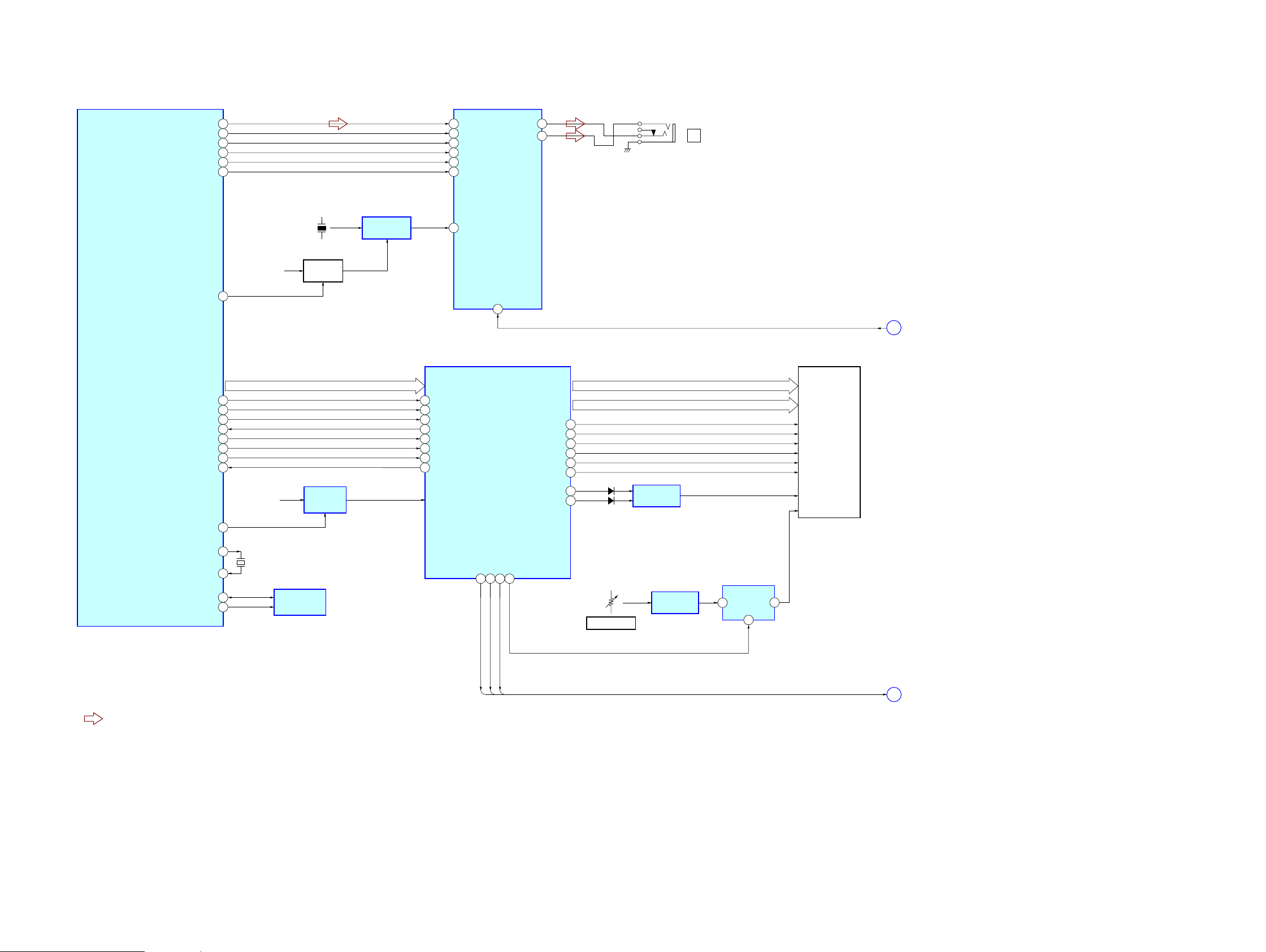
6-1. BLOCK DIAGRAM - MAIN Section (1/2) -
(Page 14)
(Page 13)
SECTION 6
DIAGRAMS
PRS-505
PRS-505
1313
MAN CPU
IC1001 (2/3)
STBY
B11
SRA3P
C10
PDOE
E11
RDY
A12
PCLK
B10
LCLK
D11
FCLK
C11
ERR
A11
AUDIO3_DATA
A1
SSI_TXFS
C8
SSI_TXCLK
A8
SSI_TXDAT
F9
AUDIO1_CS
B1
AUDIO2_CLK
B2
MCKI
9
SDATA
BICK
LRCK
4
CDTI
2
CCLK
3
CS
1
5
6
AUDIO D/A
CONVERTER
IC101
X102
11.2896MHz
CLOCK BUFFER
IC107
B+ SWITCH
Q104, 105
V2
PCAUDIO
C5
INDICATOR
CONTROLLER
IC301
GDOE
43
SDOE
42
GDCLK
45
SDCLK
41
GDSP
44
SDLE
29
+1.5V
REGULATOR
IC302
VCORE
PD0 – PD15
28
95
93
94
27
26
97
96
STBY
RESET
PDOE
RDY
PCLK
LCLK
FCLK
ERR
PD0 – PD15
VCC
PCA3PCORE
E14
X1002
32.768kHz
L15
K15
EXTAL32K
XTAL32K
TEMPERATURE
SENSOR
IC1002
I2CSCL
J11
I2CSDA
H14
SDD0 – SDD7SDD0 – SDD7
SDCE0 – SDCE2SDCE0 – SDCE2
RSTN
B
IIE1
INK INDICATOR
ELEMENT
• SIGNAL PATH
: AUDIO
GMODE1, GMODE2
OE
U1CKV, U2CKV
CL
U1SPV, U2SPV
LE
D0 – D7
CE1 – CE3
RSTN
10
8PWR_GATE
8PWR_POS
8PWR_NEG
PWR2
PWR1
PWR0
PWRCOM
65
72 73 69
8PWR_NEG,
8PWR_POS,
8PWR_GATA
C
VCOM SWITCH
IC1806
CH1
6
VCOM
1
A
5
VCOM AMP
IC1807 (2/2)
VCOM VOLTAGE
RV1801
VCOM
COMPARATOR
IC1807 (1/2)
BDR1
70
VBORDER
D1809
BDR0
71
D1808
HPR
22
HPL
23
J
J002
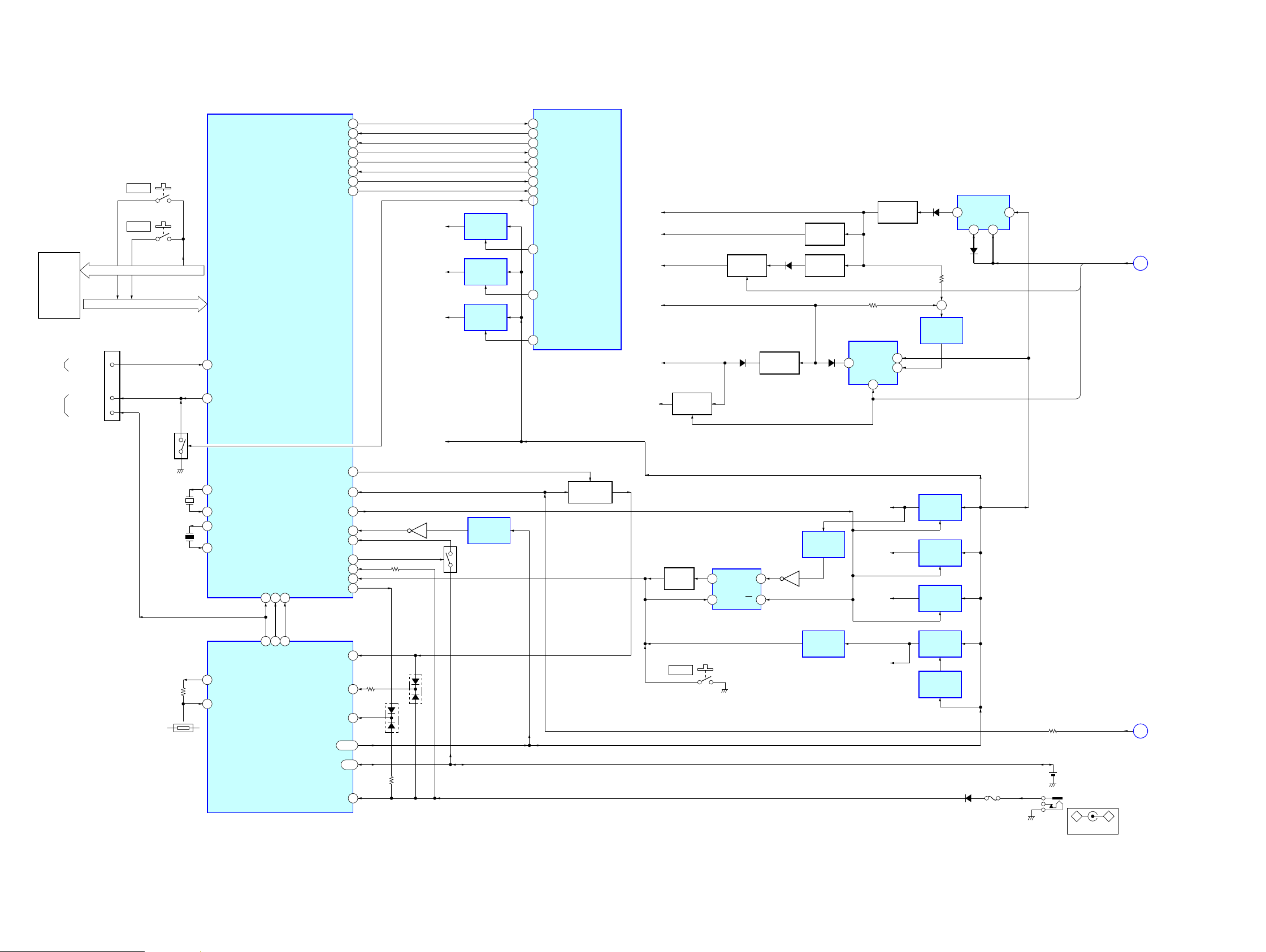
6-2. BLOCK DIAGRAM - MAIN Section (2/2) -
(Page 12)
(Page 14)
PRS-505
PRS-505
1414
S873
VOL −
S874
VOL +
SUB CPU
IC801
KEY
FLEXIBLE
BOARD
KEY_OUT0 –
KEY_OUT2
KSI0 – KSI7
KSI6
LED
SWITCH
Q1001
2
3
X801
32.768kHz
6
5
X802
4.9152MHz
X1
X2
OSC2
OSC2
STAT215DCDET
47
STAT2
3
XACPG
18
KSI7
BAT
AC
4
OUT
15 – 17
5, 6
USB
20
PSEL
8
ISET2
7
D403
D401
BATT-DC
1
AD_ON
21
BATT-LI
63
VOLTAGE
DETECTOR
IC408
LOW-BATT-LI
44
BATTERY
CONTROL SWITCH
Q801, 802
Q472
ISET2
10
RWRON
20
USBDET
43
USBON
24
XRESET
8
+3.1V
REGULATOR
IC409
V3
+1.9V
REGULATOR
IC403
VCORE
+2.9V
REGULATOR
IC402
V2
+2.9V
REGULATOR
IC406
VOLTAGE
DETECTOR
IC405
VOLTAGE
DETECTOR
IC404
Q401
VOLTAGE
DETECTOR
IC802
S801
RESET
B+ SWITCH
Q402, 405, 406
UNREG
CHARGE CONTROL
IC401
PCSDCARD
E7
PCMSCARD
F7
PCA3PIO
+3.1V
REGULATOR
IC303
+3.1V
REGULATOR
IC204
+3.1V
REGULATOR
IC205
G11
SD-VDD
MS-VCC
VDD
TXD
59
RXD
58
USBCHG
46
USBBOOT
52
XM_RESET
23
POR
22
CTS
42
RTS
57
USB_BOOT
USB_CHRG
UART1_TXD
B8
UART1_RXD
E8
UART1_RTS
C9
UART1_CTS
E9
POR
XRESET-IN
F14
H11
M14
L12
USBLED
C2
MAIN CPU
IC1001 (3/3)
KEY_IN0 –
KEY_IN7
KSO0 – KSO2
KSO0
SWITCHING
REGULATOR
IC1802
SW
1
SHDN
4
VIN
6
B+ SWITCH
Q1804
REGULATOR
Q1806
REGULATOR
Q1802
B+ SWITCH
Q1805, 1822
REGULATOR
Q1809
CURRENT
DETECT
IC1803
B− SWITCH
Q1814
DC/DC CONVERTER
IC1805
SW
1
NFB
3
VIN
5
8PWR_NEG
8PWR_GATE
8PWR_POS
VPOS
VGP
GVDD
VEE, GVSS
GVCC
D1801
VNEG
C
8PWR_NEG,
8PWR_POS,
8PWR_GATA
SS
5
D1810
D1804
D1802
SHDN
4
D1805
+
LITHIUM ION
BATTERY
3.7V 600mAh
J001
VBUS
A
–
+
DC IN 5.2V
PS401D1805
V1
CK
1
RESET
IC407
Q
5
CLR
6
PR
7
BUFFER
Q403
STBY_SW
48
LED_1
50
4
1
SW-STBY
ORG LED2
CN201
2
RED LED1
FROM
POWER
SWITCH
TO
LED
STAT1
14
STAT1
2
LDO1
TS12
THP401
(Page 13)
6-3. BLOCK DIAGRAM - KEY/POWER SUPPLY Section -
(Page 12)
PRS-505
PRS-505
1515
For Schematic Diagrams.
Note:
• All capacitors are in μF unless otherwise noted. (p: pF)
50 WV or less are not indicated except for electrolytics
and tantalums.
• All resistors are in Ω and 1/4 W or less unless otherwise
specifi ed.
• f : internal component.
• C : panel designation.
THIS NOTE IS COMMON FOR PRINTED WIRING BOARDS AND SCHEMATIC DIAGRAMS.
(In addition to this, the necessary note is printed in each block.)
• A : B+ Line.
• B : B– Line.
• C : adjustment for repair.
• Power voltage is dc 5.2V and fed with regulated dc power
supply from TP402 and TP400 on the MAIN board.
• Voltages and waveforms are dc with respect to ground
under no-signal (detuned) conditions.
no mark
: POWER ON
( ) : AUDIO PLAY
* : Impossible to measure
(For this model, the voltage is produced only when the
screen is changed. Under the power on, there is a voltage
that is not produced.)
• Voltages are taken with VOM (Input impedance 10 MΩ).
Voltage variations may be noted due to normal production
tolerances.
• Waveforms are taken with a oscilloscope.
Voltage variations may be noted due to normal production
tolerances.
• Circled numbers refer to waveforms.
• Signal path.
F : AUDIO
L : VIDEO
N : USB
O : SD MEMORY CARD/MEMORY STICK DUO
For Printed Wiring Boards.
Note:
• Y : Parts extracted from the conductor side.
• f : internal component.
• : Pattern from the side which enables seeing.
(The other layers' patterns are not indicated.)
Caution:
Parts face side:
(Conductor side)
Pattern face side:
(Component side)
Parts on the parts face side seen from
the pattern face are indicated.
Parts on the pattern face side seen from
the parts face are indicated.
Note:
The components identifi ed by mark 0 or dotted
line with mark 0 are critical for safety.
Replace only with part
number specifi ed.
Note:
Les composants identifi és
par une marque 0 sont
critiques pour la sécurité.
Ne les remplacer que par
une piéce portant le numéro spécifi é.
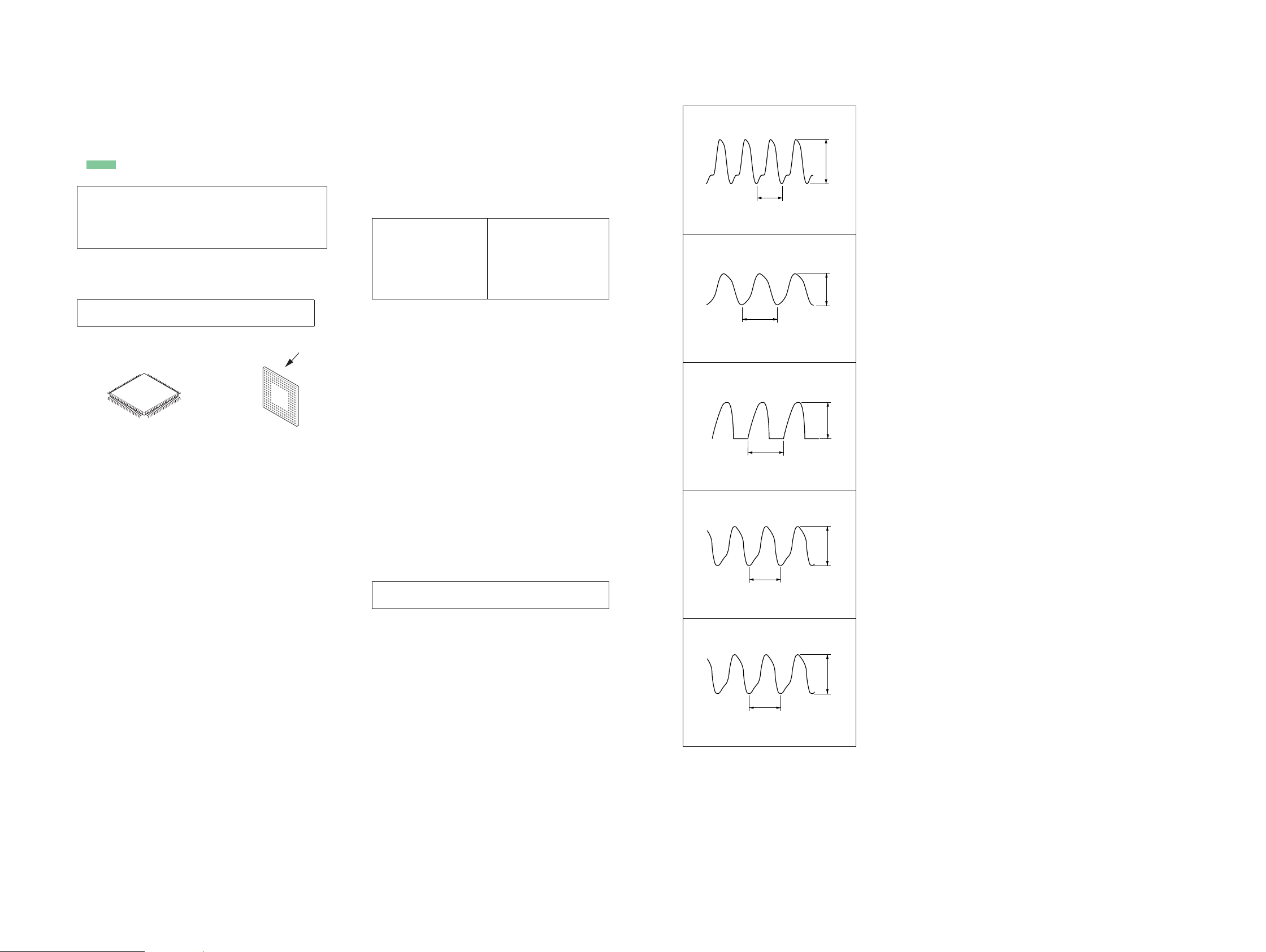
• Waveforms
– MAIN Board –
• MAIN board is multi-layer printed board.
However, the patterns of intermediate-layers have not been in-
cluded in diagrams.
• Lead layouts
surface
CSP (Chip Size Package) Lead layout of conventional IC
* Replacing of IC1001 on the MAIN board used in this
set requires a special tool.
• The voltage and waveform of CSP (chip size package) cannot be
measured, because its lead is different feom that conventional
IC.
* Replacing of IC1001 on the MAIN board used in this
set requires a special tool.
IC107
(Audio play mode)
2 V/DIV, 50 ns/DIV
C
IC953 (XO)
L
(USB connection state)
55.2 ms
1 V/DIV, 20 ms/DIV
IC1001 (XTAL32K)
K
[C
30.6 Ms
200 mV/DIV, 10 Ms/DIV
IC801 (X2)
30.8 Ms
1 V/DIV, 20 Ms/DIV
IC801 (OSC2)
3.6 Vp-p
89 ns
2.2 Vp-p
0.6 Vp-p
2.2 Vp-p
204 ns
3.1 Vp-p
1 V/DIV, 100 ns/DIV
PRS-505
PRS-505
1616
R402
R403
R210
R404
R405
R406
R407
C1120
R408
C1121
R409
C1124
C1125
R219
RB2001
RB2002
RB2003
RB2004
R411
RB2005
CN201
Q472
RB2006
R413
RB2007
R1103
R414
RB2008
R415
RB2009
R416
R223
R417
R224
R418
R419
R801
IC1101
R802
IC1102
R803
RB2010
R804
RB2011
R805
CN401
RB2012
R806
IC1106
IC1107
RB2013
R807
R420
RB2014
R808
IC1108
R421
RB2015
R809
R422
RB2016
R423
R424
R425
R426
R427
R428
R810
R429
R811
IC1112
R812
IC1113
R813
R814
R815
IC1116
IC1117
R816
L1002
R817
L1003
R430
L1004
R431
R819
C201
C202
IC953
C203
R240
C204
T951
R241
C205
CN801
R242
C206
R243
C207
R244
C208
R245
R821
C209
L1201
R246
R822
L1202
R247
R248
R824
R249
R825
C401
R826
C402
R827
C403
R828
C210
C404
R829
C211
C405
C212
C406
C213
C407
R250
C214
C408
R251
C215
R252
C216
R253
C217
R1907
R254
C218
R1908
R255
C219
R833
C411
R836
C412
R837
C413
C220
R1910
C221
C222
C416
C223
C417
C418
C225
C419
C801
C226
C802
C227
C803
R840
C228
C804
C805
R842
C806
C807
C420
C808
C421
C809
C422
C423
L1803
C424
L1804
C425
C426
C427
C810
C811
C429
X801
C812
X802
C813
R851
C430
L1811
R856
L1812
R857
R2101
R2102
R2103
R2104
R475
R2105
R477
S801
C449
R2119
Q104
Q105
D401
D402
L102
D403
L103
TP354
RB301 RB302 RB303
RB304
L301
R2527
IC201
IC202
IC203
IC204
IC205
IC206
D802
RV1801
D420
IC401
IC402
IC403
IC404
IC405
IC406
IC407
IC408
IC409
IC801
IC802
C1003
C1004
C1005
Q1001
C1006
C1007
C1008
C1009
C1200
R101
R102
C1202
S873
R103
C1203
S874
C1010
R104
C1204
C1011
C1205
C1012
R106
C1206
C1013
R107
C1014
R108
C1208
C1015
R109
C1209
C1016
C1017
C1018
C1019
R301
R302
R303
R110
C1211
C1213
C1020
C1214
C1021
C1022
R116
C1023
R117
C1217
C1024
C1218
C1025
C1219
C1028
C1029
R120
C1220
C1221
R122
C1030
C1031
C1801
IC1001
C1032
IC1002
C1033
C1034
C1804
C1035
R129
C1805
C1036
C1806
Q1802
CN302
C1808
Q1804
C1809
Q1805
R322
Q1806
Q1809
IC1201
R326
IC1202
R327
IC1203
R328
C1810
L951
THP401
L952
C1812
L953
C1814
C1816
R330
C1818
Q1814
C1819
R333
C103
R334
C104
R337
C107
C108
C1821
C109
L1101
C1822
L1102
C1823
C301
D1801
Q1822
C302
D1802
C303
D1803
C110
C304
D1804
C111
C305
D1805
CN901
C112
C306
R1802
X102
C113
D1807
C114
C308
D1808
C115
C309
D1809
C116
C117
R1807
C118
R349
C119
IC1802
IC1803
C1834
C310
D1810
C1835
C311
IC1805
C312
IC1806
D1813
C313
IC1807
C120
C314
C121
C315
C122
C316
C123
C317
C124
C318
R1814
R355
C319
R1815
R1816
C128
C129
C1842
C1843
C1844
C320
C1845
C321
C322
C323
C324
C325
R1821
C326
R1823
R364
R1824
R365
R1826
R1827
R1828
R1829
C1855
C141
R1832
TP802
R1835
R376
R1836
R377
R1837
R378
R954
R379
R956
R957
R958
R959
C1866
R380
R1840
R2010
R381
R1841
R382
R1842
R1843
R383
R2013
R384
R960
R1844
R2208
R385
R961
R1845
R386
R962
R1846
R387
R1847
R388
R1848
R389
R965
R1849
R2019
R967
R968
R969
R2020
R2214
C1879
R2021
R2215
D101
R2216
D102
R970
R971
R2219
TP829
C1884
C1885
R1860
TP830
R1861
RB201
Q401
RB202
Q402
R1863
RB203
Q403
R1864
Q405Q406
L201
L203
L204
L205
L206
L207
IC101
C954
R2238
C955
R2239
R1876
C956
L402
C957
IC107
L403
C958
IC108
C959
Q801
Q802
IC301
IC302
IC303
R1880
C960
R1881
C961
X951
R1882
C962
R1883
C963
R1884
C964
R1885
C965
RB801
R1886
C966
RB802
R1887
C967
RB803
R1888
C968
RB804
R1889
C969
RB805RB806
RB807
RB808
L801
R1890
C970
R1891
R1892
R1893
R1894 R1895
R1898
R1899
R2264
R2267
R2268
C1101
PS401
X1002
C1103
C1104
C1108
C1109
R203
C1110
R204
R205
C1112
R206
C1113
R207
C1114
R208
C1115
R209
R1298
∗
A
CONNECT
FLEXIBLE
BOARD
MAIN BOARD (COMPONENT SIDE)
1-875-228-
11
18
1
1
24
48
25
1
1
8
16
9
1
1
1
4
8
5
1
4
8
5
25
26 50
75
76100
51
26
50
50 75
100
125
76
4
8
5
24
48 25
139
238
1
1
15
34
3
54
8
169
1
124
3
16
48 33
32
17
49
64
112
1
123
456
789
10 11 12
13 15 14
16 18 17
19 21 20
22 24 23
27 25 26
52 53 54
49 50 51
46 47 48
43 44 45
41 40 42
37 38 39
34 35 36
31 32 33
29 30 28
123
456
789
10 11 12
13 15 14
16 18 17
19 21 20
22 24 23
27 25 26
52 53 54
49 50 51
46 47 48
43 44 45
41 40 42
37 38 39
34 35 36
31 32 33
29 30 28
1
10
20
11
1
1
1
3
1
2
3
6
5
4
12
3
654
5
4
1
3
5
4
4
85
10
20
11
102011
1
102011
1
2
1
30
VOL +
VOL –
22
28
14
15
21
71
13
5
C
B
E
C
BE
4
13
54
8
K
A
K
A
KA
A1B1C1D1E1F1G1 H1
A2B2C2D2E2F2G2 H2
A3B3C3D3E3F3G3 H3
A4B4C4 F4G4 H4
A5B5C5 F5G5 H5
A6B6C6D6E6F6G6 H6
A7B7C7D7E7F7G7 H7
A8B8C8D8E8F8G8 H8
D
GS
D
GS
KAKAK
A
C
B
E
C
B
E
1
11020
21
11
2919
12
354
RESET
K
A
A
124
3
124
3
124
3
135
4
6
143
12
43
12
43
12
43
4
5
1
8
463
1
52
K
K/A
A
KA
K
K/A
A
K
A/K
A
K
A/K
A
KAKA
KA
KA
K
A
C
B
E
D
G
S
C
B
E
C
B
E
C
B
E
C
BE
C
BE
1
2
3
6
5
4
81
5
4
12
43
12
43
12
43
SLOT
FLEXIBLE
BOARD
IIE1
INK
INDICATOR
ELEMENT
D
G
S
KEY
FLEXIBLE
BOARD
R1 P1 N1 M1 L1 K1 J1 H1 G1 F1 E1 D1 C1 B1 A1
R2 P2 N2 M2 L2 K2 J2 H2 G2 F2 E2 D2 C2 B2 A2
R3 P3 N3 M3 L3 K3 J3 H3 G3 F3 E3 D3 C3 B3 A3
R4 P4 N4 M4 L4 K4 J4 H4 G4 F4 E4 D4 C4 B4 A4
R5 P5 N5 M5 L5 K5 J5 H5 G5 F5 E5 D5 C5 B5 A5
R6 P6 N6 M6 L6 K6 J6 H6 G6 F6 E6 D6 C6 B6 A6
R7 P7 N7 M7 L7 K7 J7 H7 G7 F7 E7 D7 C7 B7 A7
R8 P8 N8 M8 L8 K8 J8 H8 G8 F8 E8 D8 C8 B8 A8
R9 P9 N9 M9 L9 K9 J9 H9 G9 F9 E9 D9 C9 B9 A9
R10P10N10 M10 L10 K10 J10 H10 G10 F10 E10D10C10 B10 A10
R11P11N11 M11 L11 K11 J11 H11 G11 F11 E11D11C11 B11 A11
R12P12N12 M12 L12 K12 J12 H12 G12 F12 E12D12C12 B12 A12
R13P13N13 M13 L13 K13 J13 H13 G13 F13 E13D13C13 B13 A13
R14P14N14 M14 L14 K14 J14 H14 G14 F14 E14D14C14 B14 A14
R15P15N15 M15 L15 K15 J15 H15 G15 F15 E15D15C15 B15 A15
LITHIUM
ION BATTERY
3.7V 600mAh
135
4
KA
K
A
A
A
B
C
D
E
F
G
H
I
123456789101112 13
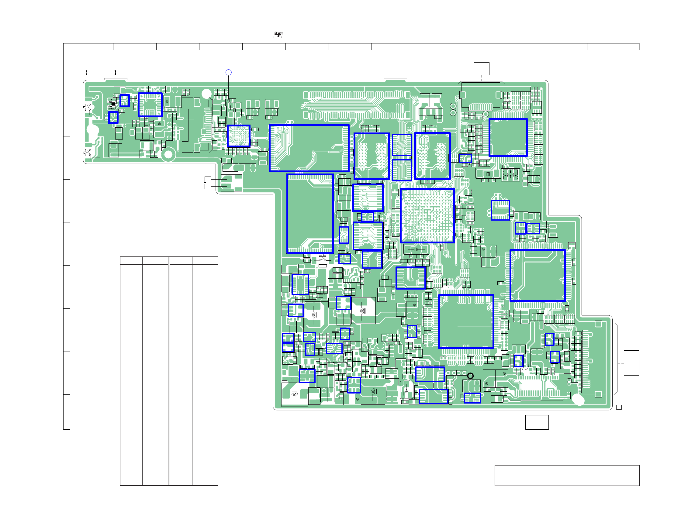
6-4. PRINTED WIRING BOARD - MAIN Board (Component Side) -
• : Uses unleaded solder.
(Page 28)
Note: When IC301, IC953, IC1106, IC1201, IC1202 and IC1203
on the MAIN board is damaged, exchange the new MAIN
board for the MAIN board which IC damaged.
Ref. No. Location
• Semiconductor Location
D101 B-3
D102 B-3
D401 F-6
D402 F-7
D403 F-6
D420 C-4
D802 B-11
D1801 I-7
D1802 G-8
D1803 I-6
D1804 H-8
D1805 H-7
D1807 H-8
D1808 H-10
D1809 H-9
D1810 H-7
D1813 H-7
IC101 B-2
IC107 B-2
IC108 B-1
IC201 F-11
IC202 E-11
IC203 D-10
IC204 G-12
IC205 H-12
IC206 E-11
IC301 G-10
IC302 G-8
IC303 H-11
IC401 F-6
IC402 G-6
IC403 F-7
IC404 G-6
IC405 G-6
IC406 G-6
IC407 G-7
IC408 G-6
IC409 G-7
IC801 C-11
Ref. No. Location
IC802 C-10
IC953 B-4
IC1001 D-9
IC1002 F-8
IC1101 C-8
IC1102 C-8
IC1106 D-6
IC1107 E-8
IC1108 E-7
IC1112 E-7
IC1113 D-7
IC1116 E-7
IC1117 D-7
IC1201 C-9
IC1202 C-7
IC1203 C-6
IC1802 H-7
IC1803 H-9
IC1805 H-6
IC1806 I-10
IC1807 I-9
Q104 C-2
Q105 C-3
Q401 G-6
Q402 F-7
Q403 G-7
Q405 F-7
Q406 F-7
Q472 H-6
Q801 C-10
Q802 C-10
Q1001 D-10
Q1802 H-9
Q1804 H-8
Q1805 G-8
Q1806 H-8
Q1809 H-7
Q1814 H-7
Q1822 H-8
PRS-505
PRS-505
1717
TP109
TP301
TP302
TP303
TP110
TP304
TP305
TP112
TP306
TP113
TP307
TP308
TP309
TP1201
TP1202
TP310
TP311
TP1016
TP312
TP1017
TP313
TP1018
TP314
TP1019
TP315
TP316
TP317
TP318
TP319
TP1022
TP1023
TP1024
TP320
TP1025
TP321
TP322
TP1027
TP323
TP1028
TP324
TP1029
TP325
TP326
TP327
TP328TP329
TP330
TP331
TP332
TP333
TP334
TP335
TP336
TP337
TP338
TP339
TP1813
TP340
TP1814
TP341
TP1815
TP342
TP1816
TP343
TP344
TP345
TP346
TP347
TP348
TP349
TP350
TP351
TP352
TP353
TP2001
TP2002
TP2003
TP2004
TP2005
TP2006
TP2007
TP2008
TP2009
TP2010
TP2011
TP951
TP952
TP953
TP954
TP955
TP956
TP957
TP958
TP959
TP960
TP201
TP202
TP203
TP204
TP205
TP206
TP207
TP208
TP209
TP1101
TP1102
TP400
TP401
TP402
TP403
TP210
TP404
TP211
TP405
TP212
TP406
TP213
TP407
TP214
TP408
TP215
TP409
TP216
TP217
TP218
TP219
TP410
TP411
TP412
TP413
TP220
TP221
TP415
TP222
TP223
TP224
TP225
TP801
TP226
TP1506
TP227
TP1507
TP1508
TP1509
TP805
TP806
TP807
TP808
TP809
TP1510
TP1511
TP1512
TP1513
TP810
TP1515
TP811
TP1516
TP812
TP1517
TP813
TP1518
TP814
TP1519
TP815
TP816
TP817
TP1520
TP1521
TP1522
TP1523
TP828
TP831
TP832
TP833
TP1540
TP1541
TP1542
TP1543
TP1544
TP1545
TP1546
TP1547
TP1548
TP1549
TP1550
TP1551
TP1552
TP1553
TP1554
TP1555
TP1556
TP1557
TP1558
TP1559
TP1560
TP1561
TP1562
TP1563
TP1564
TP860
TP1565
TP1566
TP1567
TP1568
TP1569
TP1570
TP1571
TP1572
TP1573
TP1574
TP1575
TP1576
TP1577
TP1578
TP1579
TP1580
TP1581
TP1582
TP1583
TP1584
TP1585
TP1586
TP1587
TP1588
TP1589
TP1590
TP1591
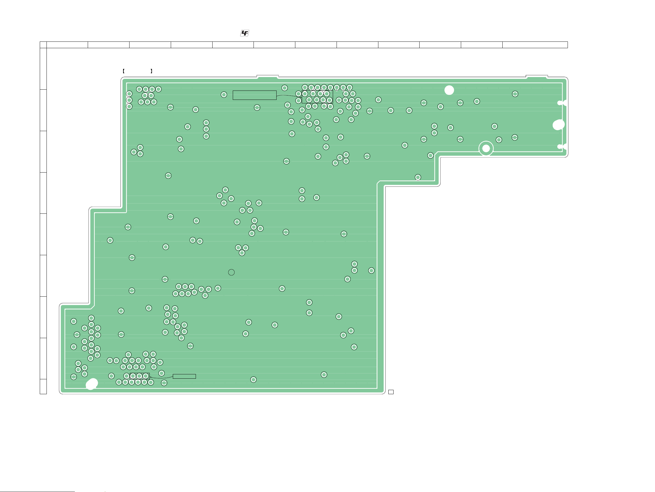
MAIN BOARD (CONDUCTOR SIDE)
1-875-228-
11
A
B
C
D
E
F
G
H
I
1234567891011 12
6-5. PRINTED WIRING BOARD - MAIN Board (Conductor Side) -
• : Uses unleaded solder.
PRS-505
PRS-505
1818
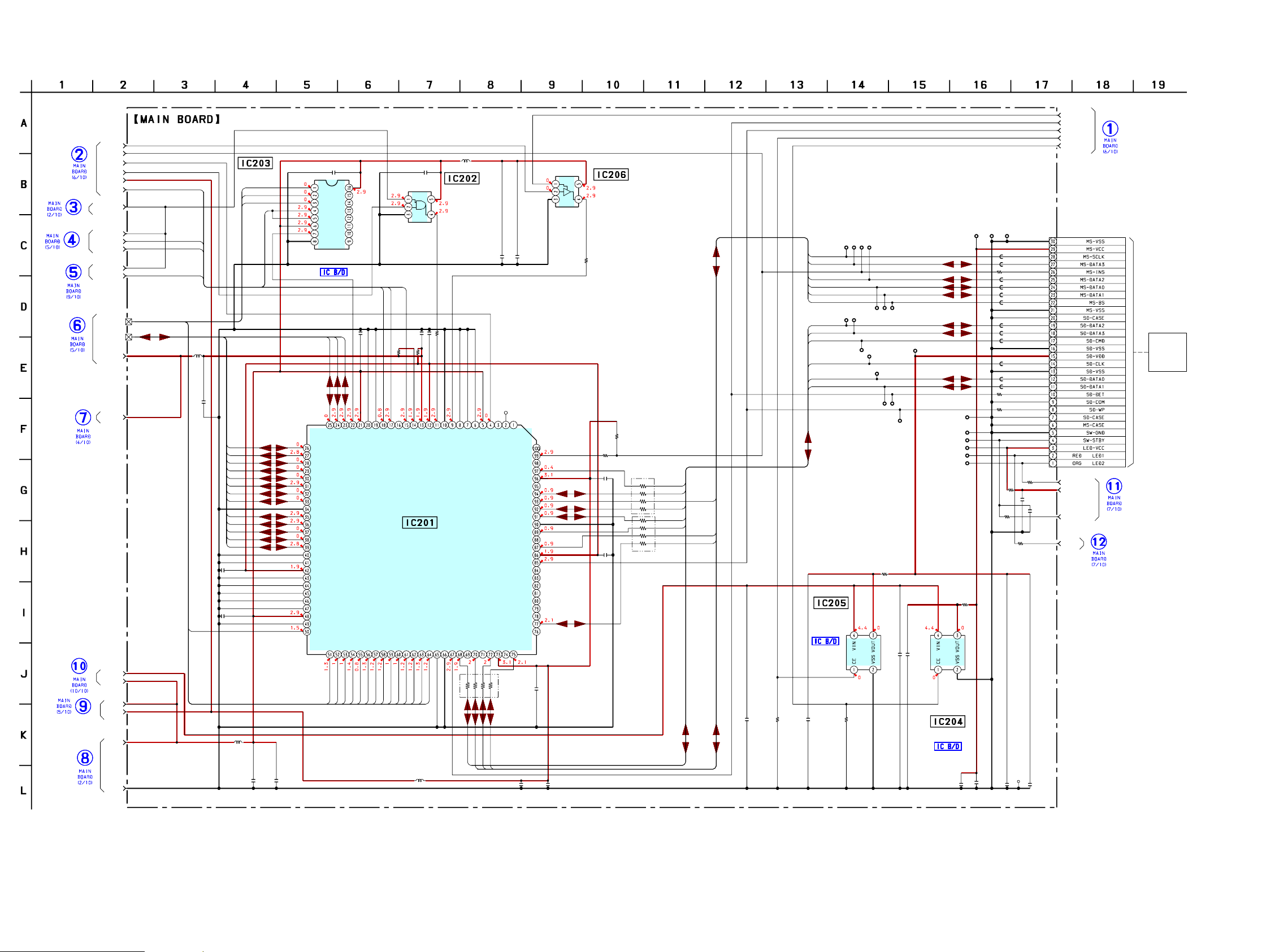
6-6. SCHEMATIC DIAGRAM - MAIN Board (1/10) -
• See page 29 for IC Block Diagram. • See page 34 for IC Pin Function Description.
TP201
TP219
TP222
TP223
TP210 TP211
TP218
TP224
TP225
TP226
TP227
IC204
IC202
IC203
IC206
C227
C207
C225
C226
R223
C210C208
L203
C214 C215
L201
C202 C206
RB202
C211
C213
C212
R210
R219
RB201
R252
R246
TP212
TP213
TP221
R247
R208
R207
R209
C228
R206
C223C222C221C220
C216 R255 C217 R224
C218
IC205
C219
IC201
TP202
TP203
TP204
TP205
TP206
TP207
TP208
C205
L204
CN201
R203 R204
RB203
TP220TP217
TP216
TP215
TP214
R254
R253
R251
R250
R249
R248
R244
R243
R242
R241
R240
R245
TP209
L205
L206
C201
C209
C204
R205
C203
L207
XC6213B312NR
TC7SH08FU
TC74LCX138FK
TC7SZ125FU
0.01
0.1
0.001
0.1
100
0.10.1
10 0.1
10 0.1
100
0.1
0.1
0.1
100
100k
100
0
0
0
220
220
0
0.1
1k
0.1100.110
1 470k 1 470k
1
XC6213B312NR
1
R5C807
0.1
30P
00
100
0
0
0.1
10
0.1
0
0.1
BD(31-0)
BA(24-0)
MSDET
GND
V2
BHRESET
SDDET
SDWP
SDINT
CS3
V3
VCORE
SRR5C
PCR5CCLK
PCR5C
PCMSCARD
PCSDCARD
LED-VCC
SW-STBY
LED2-ORG
STAT1
CLKO
V3
BHRESET
BOE
BEB2
BHRESET
VCORE
V2
UNREG
V2
BOE
BA1
BA2
BA3
BA4
BA5
BA6
BA7
BA8
BA9
BA10
BA11
BA12
BA13
BA14
BA15
BD0
BD1
BD2
BD3
BD4
BD5
BD6
BD7
BD8
BD9
BD10
BD11
BD12
BD13
BD14
BD15
SDINT
SDINT
BEB2
BEB2
BOE
DAT0
DAT1
DAT2
DAT3
CMD
CLK
BA21
BA22
BA23
CS3
CS3
DAT3
DAT0
DAT1
DAT2
CMD
CLK
MSDAT3
MSCLK
MSBS
MSBS
MSDAT1
MSDAT0
MSDAT2
MSDAT3
MSCLK
MSDAT2
MSDAT0
MSDAT1
GND
VCC
VCCEN
GPIO
LED
HWSPND
RWMODE
WAMODE
LTLEN
TEST
CKIN
GND
RST
VCC_ROUT
VCC_RIN
REGEN
INT
WAIT/DTACK
WR
RD
EB1
EB0
VCC_HOST
CS
D15
D14
D13
D12
D11
D10
D9
D8
D7
D6
D5
GND
D4
D3
D2
D1
D0
BS
A22
VCC_ROUT
A21
A19
A20
A18
A17
VCC_HOST
A16
A15
A14
A13
A12
A11
A10
A9
A8
A7
A6
A5
A4
A3
A2
A1
A0
GND
MDIO11
MDIO12
VCC_3V
MDIO14
MDIO15
MDIO21
MDIO22
MDIO19
MDIO20
MDIO23
MDIO24
VCC_ROUT
MDIO17
GND
MDIO09
VCC_3V
MDIO27
MDIO29
A
B
C
G2A
G2B
G1
Y7
GND
VCC
Y0
Y1
Y2
Y3
Y4
Y5
Y6
(1/10)
VCC
GND
FLEXIBLE
SLOT
ADDRESS
DECODER
SWITCHING
BUFFER
REGULATOR
+3.1V
+3.1V
REGULATOR
BOARD
MEMORY STICK DUO/
SD MEMORY CARD
CONTROLLER
MSCD
SDCMD
SDDAT2
MSBS
SDDAT1
SDDAT0
SDCLK
MSCLK
SDWP
MSDAT3
MSDAT2
XDCE
MSDAT1
MSDAT0
SDDAT3
SDCD
10μH
10μH
10μH
100μH
(Page 23)
(Page 19)
(Page 22)
(Page 26)
(Page 22)
(Page 21)
(Page 27)
(Page 22)
(Page 19)
(Page 24)
(Page 24)
(Page 23)
PRS-505
PRS-505
1919
IC101
IC108
C129
C128
TP112
TP109
C112 R107
C113 R108
C111
C110
C109
R106
IC107
R110
R102Q105
R103
R104
R101
C103
C104
L102
Q104
C108
R109
C122
C121 C120
C118
C117 C116
L103
C114 C115
C123
C124
C107
R117
R116
C141
TP1590
X102
R120
R122
R129
C119
D102
D101
TP110
AK4365VN-L
TC7SH08FU
220
4V
220
4V
HP-R
HPGND
0.1 10
0.1 10
10
0.1
0.0047
10k
TC7SHU04FU
470
1M2SC4738F-Y/GR
4.7k
4.7k
100k
0.001
0.1
2SA1832F-GR
0.01
10
0.1
0.1 0.1
10
10 1
0.1 10
10
0.1
0.01
100
330
0.01
11.2896MHz
10
UDZSNPTE-175.6B
UDZPTE-175.6B
HP-L
STFS
STCK
STXD
SRDSP
AUDIO1
AUDIO2
AUDIO3
PCAUDIO
HP-L
HP-GND
HP-R
BHRESET
GND
V2
GND
VCC
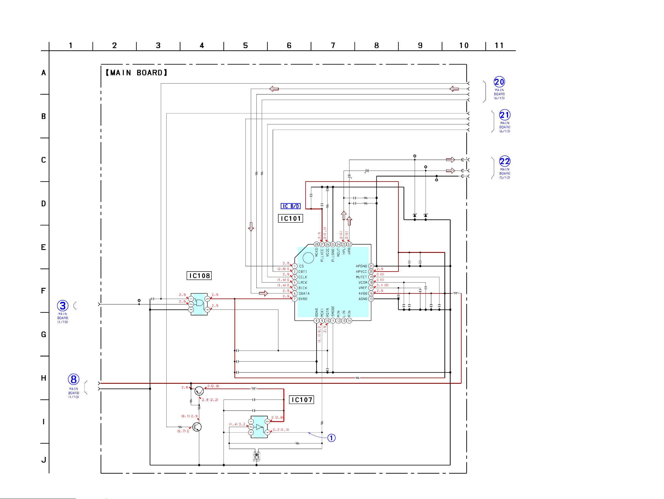
(2/10)
VCC
GND
NC
SWITCHING
B+ SWITCH
Q104,105
CLOCK BUFFER
AUDIO D/A
CONVERTER
100μH
22μH
(Page 18)
6-7. SCHEMATIC DIAGRAM - MAIN Board (2/10) -
• See page 15 for waveform. • See page 29 for IC Block Diagram.
(Page 18)
(Page 23)
(Page 23)
(Page 22)
PRS-505
PRS-505
2020
TP1815
TP1814
TP1816
TP1813
D1801
Q1804
R1816
IC1802
IC1805
D1802
D1804
D1805
Q1822
Q1809
R1843
R1802
R1884
C1816
R1907
C1808
L1811 C1804
R1824
R1823
C1806
R1835 R1836
R1883
C1801
R1837
D1803
C1843
R1894
R1895
R1893 C1845 C1818C1834
R1881
R1880
R1882
R1898 R1807
D1810
R1908
C1809
C1835
C1805
R1910
R1899
R1876
C1879
R1827
R1828
R1826 C1842 R1891
R1890
C1855
R1892
C1810
C1814
R1888
R1889
R1887
R1886
Q1805
R1885
C1844
R1846
R1845
R1844
R1847
IC1806
C1819
C1866
TP354
R1840
C1884
C1822
IC1803
D1807
R1829R1863
R1821
C1812
R1860
R1861
R1832
C1821
R1842
R1841
RV1801
R1849 R1848 R1815
Q1814
IC1807
C1885
L1812
L1803
D1813
Q1802
C1823
R1864
R1814
D1808
D1809
Q1806
L1804BAT760-115
SSM6J07FU
100k
LT3467ES6#TR
LT1931ES5#TR
1SS362-TE85L
BAT760-115
1SS362-TE85L
2SJ305(TE85L)
2SA1832F-GR
10k
0
10k
0.47
100k
10
16V
10
82k
24k
10
15k 27k
10k
0.0022
240
BAT760-115
0.1
24k
27k
100k 0.1 11
100k
10k
10k
1k 10k
1SS388(TPL3)
100k
10
16V 0.47
10
0
100
10k
0.01
91k
30k
11k 0.1 33k
22k
0.1
100k
1
1
100k
10k
56k
56k
2SC4738F-Y/GR
100k
0.1
1k
15k
30k
1M
TC7W53FK
0.1
100
6.3V
3.3k
0.1
0.1
NJM2904V(TE2)
1SS362-TE85L
1k10k
100k
0.22
100k
100k
1k
0.1
47k
4.7k
10k
1k 100k 680k
HN1B04FE-Y/GR
NJM2904V(TE2)
0.1
1SS362-TE85L
2SC4738F-Y/GR
0.1
680k
1k
1SS387-TPL3
1SS387-TPL3
2SC4738F-Y/GR
8-ROW_VCC
8-15V
8PWR_NEG
8PWR_POS
8PWR_GATE
8COM_CTRL
8BORDER0
8BORDER1
8+15V
UNREG
GND
8-V3
8-COMMON
8-BORDER
8-25V
8-5V
8--20V
UNREG
GND
VCC
CH0
CH1
AGND
VEE
INH
COM
-
V-
V+
SW
GND
NFB
SHDN
VIN
SW
SS GND
FBSHDN
VIN
V-
V+
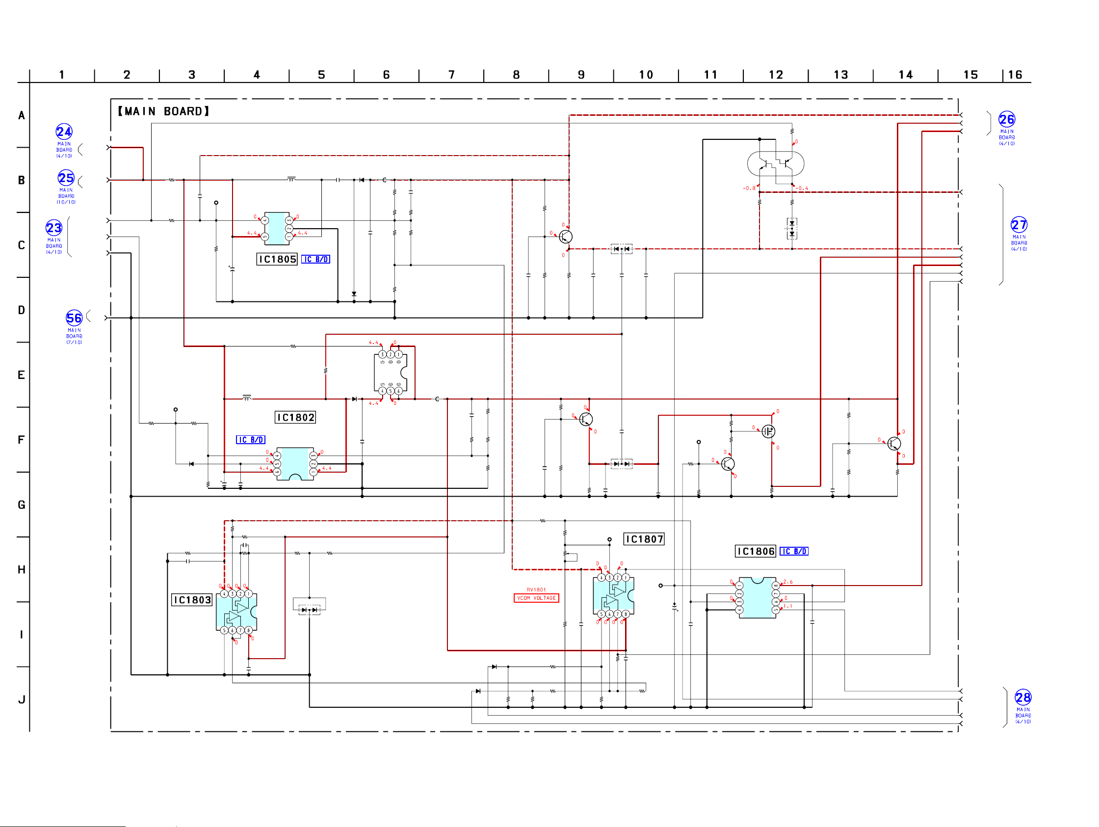
(3/10)
1
654
32
DC/DC
CONVERTER
SWITCHING
REGULATOR
CURRENT
DETECT
COMPARATOR,
VCOM AMP
VCOM SWITCH
B+ SWITCH
Q1805,1822
S
REGULATOR
REGULATOR
REGULATOR
B+ SWITCH
10μH
10μH
B− SWITCH
+
–
+
–
+
–
+
–
(Page 21)
6-8. SCHEMATIC DIAGRAM - MAIN Board (3/10) -
• See page 29 for IC Block Diagram.
(Page 27)
(Page 21)
(Page 24)
(Page 21)
(Page 21)
(Page 21)
PRS-505
PRS-505
2121
TP312
TP313
TP314
TP315
TP316
TP319
TP331
TP332
TP344 TP345
TP346
TP318
R386
IC301
TP301
TP350
TP349
C317
R330
R333
R337
C318 C320
TP302
TP303
TP304
TP305
TP306
TP307
TP308
TP309
TP310
TP311
C325
C323
C324
R389
C305
R364
C306
R388
C322
R387R355
R322
C302
C301
TP347
TP348
R302
C303
R303
C304
L301
R326
R334
R384
R383
R382
R381
R380
R379
TP325
TP324
TP323
TP322
R377
TP321
TP320
C311
C310
C309
C314
TP327
TP329
TP330
C308
R376
R378
C313
C312
R328
C316
C315
CN302
TP328
TP334
TP335
TP336
TP337
TP338
TP339
TP340
TP341
TP342
TP343
TP326
TP333
R385
R301
C321
R349
RB303
RB301
IC303
R327
R365
C319
RB302
TP353
TP352
TP351
RB304
C326
TP317
IC302
0
A3P125-VQG100
0.1
0
330
330
0.1 0.1
0.1
0.1
0.1
1k
0.1
1k
0.1
1k
0.1
1k0
470k
1
1
470k
1
0
1
0
100
0
0
0
0
0
0
0
10
0.1
1
0.1
0.1
0
0
4.7
25V
4.7
25V
0
0.1
0.1
39P
0
0
0.1
100
100
100
XC6215B312NR
0
0
0.1
100
100
10
XC6215B152NR
8PWR_GATE
8COM_CTRL
8-BORDER
8-ROW_VCC
8-25V
8--20V
8-COMMON
8-5V
8+15V
8-15V
GND
VCORE
UNREG
PCA3PIO
PCA3PCORE
8-V3
LCDBUS
8BORDER0
8BORDER1
8PWR_POS
8PWR_NEG
VCORE
GND
PD0
PD1
PD2
PD3
PD4
PD5
PD6
PD7
PD8
PD9
PD10
PD11
PD12
PD13
PD14
PD15
FCLK
LCLK
PCLK
ERR
STBY
RDY
PDOE
SDLE
SD0
SD1
SD2
SD3
SD4
SD5
SD6
SD7
SDCLK
SDOE
GDOE
GDSP
GDCLK
SDCE0
SDCE1
SDCE2
SDCLK
SDLE
GDOE
GDSP
GDCLK
8COM_CTRL
8BORDER0
8BORDER1
8PWR_POS
8PWR_NEG
8PWR_GATE
SRA3P
8BORDER0
8BORDER1
8PWR_POS
8PWR_NEG
8PWR_GATE
8COM_CTRL
SDCE1
SDCE0
SD0
SD1
SD2
SD3
SD4
SD5
SD6
SD7
SDOE
SDCE2
GND
PD15
GND
GND
GND
GND
GND
GND
VCC
TCK
TDI
TMS
VPUMP
NC
TDO
TRST
VJTAG
VCC
GND
VCC
PD14
PD13
PD12
PD11
PD10
PD9
PD8
PD7
PD6
PD5
PD4
PD3
PD2
PD1
PD0
PSFL
VCC
FCLK
LCLK
PCLK
SDLE
SDDO0
SDDO1
SDDO2
SDDO3
SDDO4
SDDO5
SDDO6
SDDO7
SDCLK
SDOE
GDOE
GDSP
GDCLK
SDCE0
SDCE1
SDCE2
SDCE3
SDCE4
SDCE5
SDSHR
GDRL
PWRCOM
PWR2
BDR1
BDR0
PWR0
PWR1
SPIDO
SPICLK
SPIDI
SPICS
I2CSCL
I2CSDA
PWR3
RESERVED
TEST2
TEST0
TEST1
RESERVED
RESERVED
RESERVED
PDOE
RESET
RDY
STBY
ERR
RESERVED
VCCI
VMV
VCCI
VMV
VCCI
VMV
VCCIB
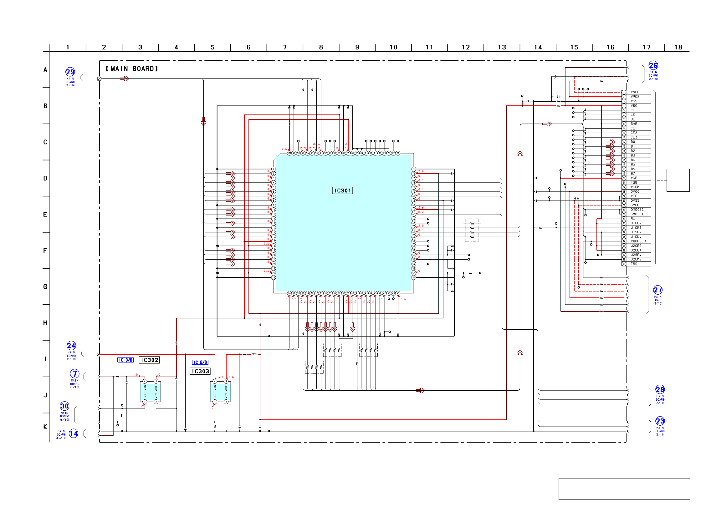
(4/10)
IIE1
INK
INDICATOR
ELEMENT
INDICATOR CONTROLLER
REGULATOR
+3.1V
+1.5V REGULATOR
GND
VMV
GND
GND
GND
10μH
6-9. SCHEMATIC DIAGRAM - MAIN Board (4/10) -
• See page 29 for IC Block Diagram. • See page 34 for IC Pin Function Description.
Note: When IC301 on the MAIN board is damaged, ex-
change the new MAIN board for the MAIN board
which IC damaged.
(Page 27)
(Page 23)
(Page 18)
(Page 20)
(Page 23)
(Page 20)
(Page 20)
(Page 20)
(Page 20)
PRS-505
PRS-505
2222
TP954
TP958
TP959
TP960
TP952
TP953
R957
IC1203
IC1106
TP1101
C1113
TP1102
C1124 C1125
L1202
C1220
C1221
TP1202
IC1108
L1102
C954
C955 C956 C957 C958 C959 C960 C961 C962 C963 C964
L951
L952
L953
TP951
X951
C965
R962
R961
R960
R959
C966
TP956
TP957C967
R965
C968
R956
R958
R967
C970
R968 R970
R969
C969
R954
C1206
IC953
TP955
C1120 C1121
CN901
T951
R971
TP1544
TP1545
DD
CVDD
0
S29AL016D
90TFI020H-PRS02
K9F2G08U0A-PCB0T
NAND
GND
0.1
GND
0.1 0.1
10
0.1
GND
TC7WZ32FK
10
10 10 0.1 0.1 0.1 0.1 0.1 0.1 0.1 0.1
LVDD
12MHz
15p
6.2k
100k
100k
100k
18p
1
10
0.01
0
0
100k
0.1
100k 82k
82k
0.1
330
0.1
S1R72V17
10 0.1
18P
INSTANCE
USB_VBUS
USBDET
VBUS
HRESET
CS4
V3
USB20INT
HP-L
HP-GND
HP-R
DC+
DC-
VCORE
#CS0
RY/#BY
BD(31-0)
BR/W
CS1
NAND-CE0
NAND-CLE
NAND-ALE
GND
BHRESET
BEB2
BOE
BOE
BEB2
BD(31-0)
V2
V3
BA(24-0)
BA(24-0)
BD1
BD2
BD3
BD4
BD5
BD6
BD7
BD8
BD9
BD10
BD11
BD12
BD13
BD14
BD15
BD0
BEB2
BOE
USBINT
CS4
BA2
BA3
BA4
BA5
BA6
BA7
BA8
BA9
BA10
BA11
BA12
BA13
BA14
BA15
BA16
BA18
BA19
BA20
BA17
BA1
BA1
BA2
BA3
BA4
BA5
BA6
BA7
BA8
BD15
BD7
BD14
BD6
BD13
BD5
BD12
BD4
BD11
BD3
BD10
BD2
BD9
BD1
BD8
BD0
BEB2
BOE
CS4
USBINT
BD0
BD1
BD2
BD3
BD4
BD5
BD6
NAND_CE0
NAND_CLE
NAND_ALE
HRESET
HRESET
NAND_CE0
NAND_CLE
NAND_ALE
BD7
GND
VCC
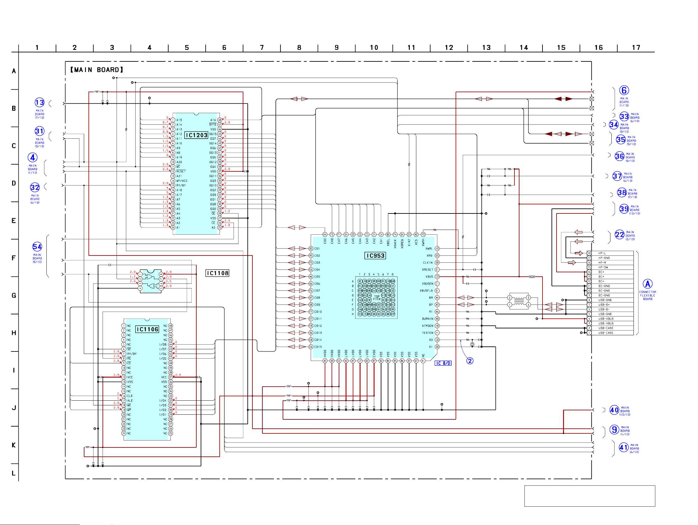
(5/10)
NOR FLASH
MEMORY
MEMORY
OR GATE
USB CONTROLLER
NAND FLASH
22μH
22μH
10μH
10μH
10μH
CSP
(Chip Size Package)
R1298
470k
(Page 24)
6-10. SCHEMATIC DIAGRAM - MAIN Board (5/10) -
• See page 15 for waveform. • See page 29 for IC Block Diagram.
Note: When IC953, IC1106 and IC1203 on the MAIN
board is damaged, exchange the new MAIN board
for the MAIN board which IC damaged.
(Page 26)
(Page 18)
(Page 23)
(Page 26)
(Page 23)
(Page 18)
(Page 27)
(Page 28)
(Page 19)
(Page 27)
(Page 24)
(Page 23)
(Page 26)
(Page 26)
(Page 26)
(Page
23)
(Page 18)
PRS-505
PRS-505
2323
TP1016
TP1017
TP1018
TP2006
TP2008
TP2007
TP1022
TP1024
TP1025
TP2011
R2105
R2102
Q1001
TP1023
R2010
C1029
RB2015 C1030
RB2014
R2527
R2216
L1002
L1003
C1005
C1006
C1003
C1004 TP1019
C1007
C1008 C1009 C1010 C1011 C1012
RB2010
RB2009
RB2008
C1013
C1014
C1015
C1016 R2268 C1017 C1018 L1004
R2119
R2215
C1019
R2208
C1022
C1021
C1020
R2267
R2239
R2219
R2238
TP2001
TP2002
TP2003
TP2004
R2264
TP2009
R2101
R2021
C1023
R2013
R2019
RB2016
C1024
R2020
TP2010
RB2005
RB2003
RB2004
RB2002
RB2001
RB2006
TP113
C1031
R2214
C1034
C1035
C1036
RB2007
TP1029
TP1028
RB2013
RB2012
RB2011
C1025
TP1585
TP1540
TP1515
TP2005
C1032
C1033
TP1591
TP1027
TP1588
TP1589
TP1541
TP1586
C1028
IC1002
IC1001
R2104 R2103
X1002
V2
V2
VCORE
BOOT1
BOOT2
BOOT0
PA18
SDCKE1
RESET-SF
16M
10
1k
2SC4738F-Y/GR
PA20
680
0.1
470k 0.1
470k
330
10k
100
6.3V
0.1
47
6.3V
0.1 GND
0.1
0.1 0.1 0.1 0.1 0.1
470k
470k
470k
0.1
0.1
0.1
0.1 1 00k 0.1 1 0
10k
10k
0.1
100k
6p
6p
0.1
100k
10k
10k
10k
TDI
TCK
TMS
TDO
100k
CLKO
1k
330
0.1
100
330
470k
0.1
330
PA14
100
100
100
100
100
330
PA14
0.1
10k
0.1
0.01
0.1
100
A0
A24
330
330
330
0.1
TRST
0.01
0.1
PB20
0.1
TMP75AIDR
MC9328MXLVP20R2
100 100
32.768KHz
PCA3PCORE
PCA3PIO
LCDBUS
V3
LED2-ORG
CLKO
SDCLK
MA10
MA11
DQM3
DQM2
DQM1
DQM0
SUB-TXD
SUB-RXD
SUB-RTS
SUB-CTS
MSDET
M_RESET
POR
PCAUDIO
AUDIO2
AUDIO3
AUDIO1
GND
SDCKEO
#SDWE
#CAS
#RAS
#CS2
RY/#BY
VCORE
V2
SRDSP
STCK
STFS
STXD
VBUS
USBCRG
USBBOOT
SDWP
SDDET
SDINT
SRR5C
PCR5C
PCR5CCLK
PCSDCARD
PCMSCARD
USB20INT
CS1
CS4
CS3
CS5
EB2
HRESET
#CS0
R/#W
#OE
GND
D(31-0)
A(24-0)
NAND-ALE
NAND-CLE
NAND-CEO
A1
A2
A3
A4
A5
A6
A7
A8
A9
A10
A11
A12
A13
A14
A15
A16
A17
A18
A19
A20
A21
A22
A23
D0
D1
D2
D3
D4
D5
D6
D7
D8
D9
D10
D11
D12
D13
D14
D15
D16
D17
D18
D19
D20
D21
D22
D23
D24
D25
D26
D27
D28
D29
D30
D31
TXD
RXD
RTS
CTS
RTS
PCAUDIO
AUDIO1
AUDIO2
AUDIO3
PCAUDIO
AUDIO1
AUDIO2
AUDIO3
USBCRG
USBBOOT
USBCRG
USBBOOT
PCLK
ERR
RDY
STBY
SRA3P
PDOE
LCLK
FCLK
PD0
PD1
PD2
PD3
PD4
PD5
PD6
PD7
PD8
PD9
PD10
PD11
PD12
PD13
PD14
PD15
CTS
TXD
RXD
SDA
SCL
OS
GND
VCC
A0
A1
A2
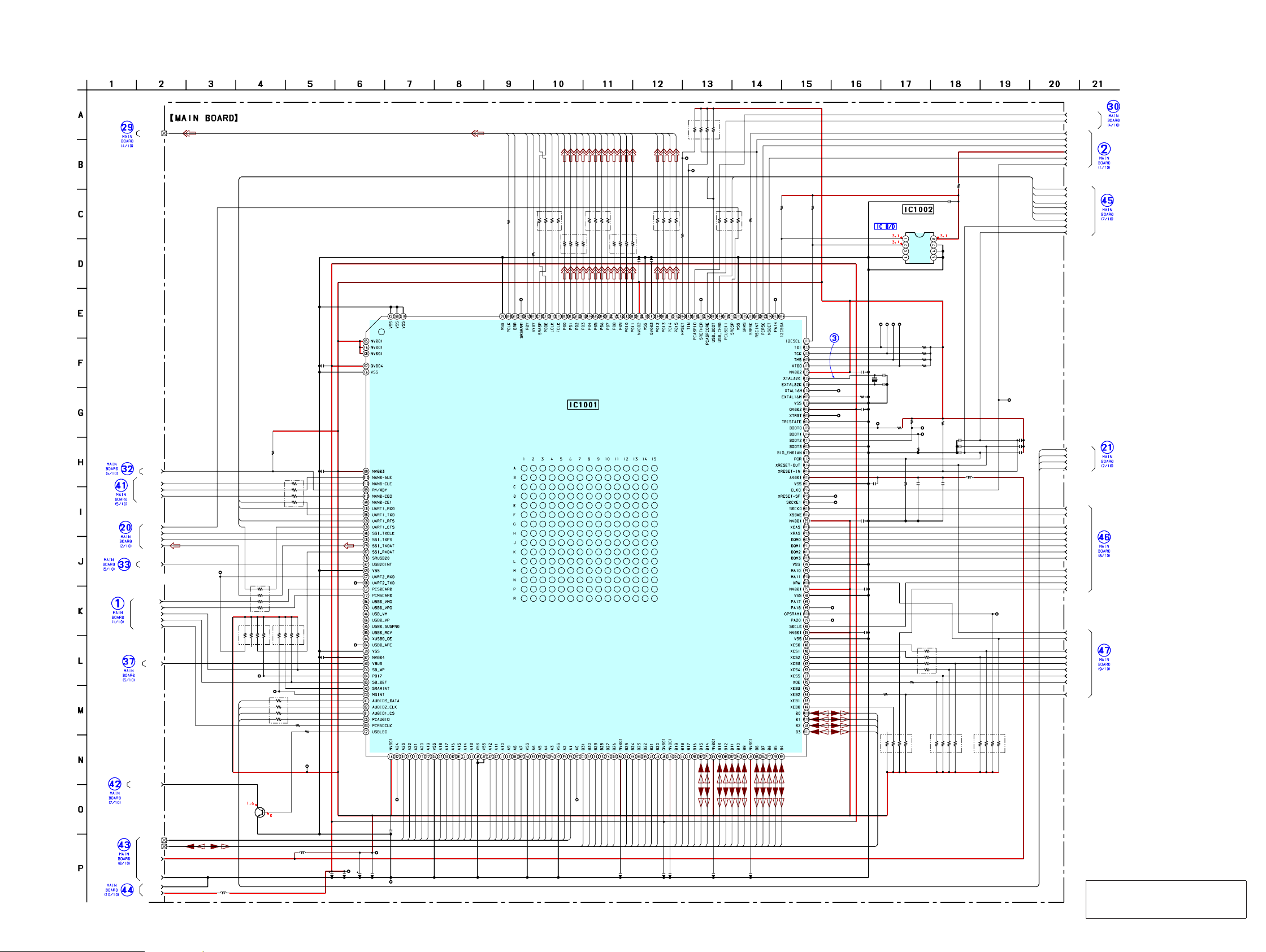
(6/10)
TEMPERATURE
SENSOR
MAIN CPU
LED
SWITCH
10μH
10μH
47μH
∗
CSP
(Chip Size Package)
6-11. SCHEMATIC DIAGRAM - MAIN Board (6/10) -
• See page 15 for waveform. • See page 29 for IC Block Diagram. • See page 34 for IC Pin Function Description.
Note: Replacement of IC1001 on the
MAIN board used in this set
requires a special tool.
(Page 21)
(Page 22)
(Page 22)
(Page
19)
(Page 22)
(Page 18)
(Page 22)
(Page 24)
(Page 25)
(Page 27)
(Page 26)
(Page 25)
(Page 19)
(Page 24)
(Page 18)
(Page 21)
 Loading...